US7186348B2 - Method for fabricating a pole tip in a magnetic transducer - Google Patents
Method for fabricating a pole tip in a magnetic transducer Download PDFInfo
- Publication number
- US7186348B2 US7186348B2 US10/882,883 US88288304A US7186348B2 US 7186348 B2 US7186348 B2 US 7186348B2 US 88288304 A US88288304 A US 88288304A US 7186348 B2 US7186348 B2 US 7186348B2
- Authority
- US
- United States
- Prior art keywords
- ion
- milling
- pole piece
- depositing
- void
- Prior art date
- Legal status (The legal status is an assumption and is not a legal conclusion. Google has not performed a legal analysis and makes no representation as to the accuracy of the status listed.)
- Expired - Fee Related, expires
Links
- 238000000034 method Methods 0.000 title claims abstract description 49
- 230000005291 magnetic effect Effects 0.000 title claims abstract description 28
- 239000000463 material Substances 0.000 claims abstract description 84
- 238000000992 sputter etching Methods 0.000 claims abstract description 77
- 239000011800 void material Substances 0.000 claims abstract description 23
- PNEYBMLMFCGWSK-UHFFFAOYSA-N aluminium oxide Inorganic materials [O-2].[O-2].[O-2].[Al+3].[Al+3] PNEYBMLMFCGWSK-UHFFFAOYSA-N 0.000 claims abstract description 13
- 238000000277 atomic layer chemical vapour deposition Methods 0.000 claims abstract description 10
- 238000000231 atomic layer deposition Methods 0.000 claims abstract description 10
- 238000000151 deposition Methods 0.000 claims description 24
- 229920002120 photoresistant polymer Polymers 0.000 claims description 22
- 239000003302 ferromagnetic material Substances 0.000 claims description 20
- 239000010409 thin film Substances 0.000 claims description 15
- 238000001020 plasma etching Methods 0.000 claims description 13
- VYPSYNLAJGMNEJ-UHFFFAOYSA-N Silicium dioxide Chemical group O=[Si]=O VYPSYNLAJGMNEJ-UHFFFAOYSA-N 0.000 claims description 10
- 239000000377 silicon dioxide Substances 0.000 claims description 5
- 239000003989 dielectric material Substances 0.000 claims description 4
- 238000004519 manufacturing process Methods 0.000 claims description 4
- OKTJSMMVPCPJKN-UHFFFAOYSA-N Carbon Chemical compound [C] OKTJSMMVPCPJKN-UHFFFAOYSA-N 0.000 claims description 3
- 229910052799 carbon Inorganic materials 0.000 claims description 3
- 235000012239 silicon dioxide Nutrition 0.000 claims 1
- 238000002360 preparation method Methods 0.000 description 7
- NJPPVKZQTLUDBO-UHFFFAOYSA-N novaluron Chemical compound C1=C(Cl)C(OC(F)(F)C(OC(F)(F)F)F)=CC=C1NC(=O)NC(=O)C1=C(F)C=CC=C1F NJPPVKZQTLUDBO-UHFFFAOYSA-N 0.000 description 5
- 229910052681 coesite Inorganic materials 0.000 description 4
- 229910052906 cristobalite Inorganic materials 0.000 description 4
- 229910052682 stishovite Inorganic materials 0.000 description 4
- 229910052905 tridymite Inorganic materials 0.000 description 4
- 230000008021 deposition Effects 0.000 description 3
- 238000000059 patterning Methods 0.000 description 3
- 229910001030 Iron–nickel alloy Inorganic materials 0.000 description 2
- 230000015572 biosynthetic process Effects 0.000 description 2
- 238000001514 detection method Methods 0.000 description 2
- 230000004907 flux Effects 0.000 description 2
- 230000001939 inductive effect Effects 0.000 description 2
- 239000012212 insulator Substances 0.000 description 2
- 239000000203 mixture Substances 0.000 description 2
- 230000007704 transition Effects 0.000 description 2
- ZAMOUSCENKQFHK-UHFFFAOYSA-N Chlorine atom Chemical compound [Cl] ZAMOUSCENKQFHK-UHFFFAOYSA-N 0.000 description 1
- 239000004642 Polyimide Substances 0.000 description 1
- 229910020776 SixNy Inorganic materials 0.000 description 1
- 238000004380 ashing Methods 0.000 description 1
- 229910052801 chlorine Inorganic materials 0.000 description 1
- 239000000460 chlorine Substances 0.000 description 1
- 229910052593 corundum Inorganic materials 0.000 description 1
- 238000005530 etching Methods 0.000 description 1
- 230000005294 ferromagnetic effect Effects 0.000 description 1
- 239000010408 film Substances 0.000 description 1
- 230000012447 hatching Effects 0.000 description 1
- 238000003384 imaging method Methods 0.000 description 1
- 230000005381 magnetic domain Effects 0.000 description 1
- 239000000696 magnetic material Substances 0.000 description 1
- 238000003801 milling Methods 0.000 description 1
- 150000004767 nitrides Chemical class 0.000 description 1
- 238000005498 polishing Methods 0.000 description 1
- 229920001721 polyimide Polymers 0.000 description 1
- 238000005070 sampling Methods 0.000 description 1
- 229910052814 silicon oxide Inorganic materials 0.000 description 1
- 238000001039 wet etching Methods 0.000 description 1
- 229910001845 yogo sapphire Inorganic materials 0.000 description 1
Images


Classifications
-
- G—PHYSICS
- G11—INFORMATION STORAGE
- G11B—INFORMATION STORAGE BASED ON RELATIVE MOVEMENT BETWEEN RECORD CARRIER AND TRANSDUCER
- G11B5/00—Recording by magnetisation or demagnetisation of a record carrier; Reproducing by magnetic means; Record carriers therefor
- G11B5/127—Structure or manufacture of heads, e.g. inductive
- G11B5/31—Structure or manufacture of heads, e.g. inductive using thin films
- G11B5/3163—Fabrication methods or processes specially adapted for a particular head structure, e.g. using base layers for electroplating, using functional layers for masking, using energy or particle beams for shaping the structure or modifying the properties of the basic layers
-
- G—PHYSICS
- G11—INFORMATION STORAGE
- G11B—INFORMATION STORAGE BASED ON RELATIVE MOVEMENT BETWEEN RECORD CARRIER AND TRANSDUCER
- G11B5/00—Recording by magnetisation or demagnetisation of a record carrier; Reproducing by magnetic means; Record carriers therefor
- G11B5/127—Structure or manufacture of heads, e.g. inductive
- G11B5/1278—Structure or manufacture of heads, e.g. inductive specially adapted for magnetisations perpendicular to the surface of the record carrier
-
- G—PHYSICS
- G11—INFORMATION STORAGE
- G11B—INFORMATION STORAGE BASED ON RELATIVE MOVEMENT BETWEEN RECORD CARRIER AND TRANSDUCER
- G11B5/00—Recording by magnetisation or demagnetisation of a record carrier; Reproducing by magnetic means; Record carriers therefor
- G11B5/127—Structure or manufacture of heads, e.g. inductive
- G11B5/31—Structure or manufacture of heads, e.g. inductive using thin films
- G11B5/3109—Details
- G11B5/3116—Shaping of layers, poles or gaps for improving the form of the electrical signal transduced, e.g. for shielding, contour effect, equalizing, side flux fringing, cross talk reduction between heads or between heads and information tracks
-
- Y—GENERAL TAGGING OF NEW TECHNOLOGICAL DEVELOPMENTS; GENERAL TAGGING OF CROSS-SECTIONAL TECHNOLOGIES SPANNING OVER SEVERAL SECTIONS OF THE IPC; TECHNICAL SUBJECTS COVERED BY FORMER USPC CROSS-REFERENCE ART COLLECTIONS [XRACs] AND DIGESTS
- Y10—TECHNICAL SUBJECTS COVERED BY FORMER USPC
- Y10T—TECHNICAL SUBJECTS COVERED BY FORMER US CLASSIFICATION
- Y10T29/00—Metal working
- Y10T29/49—Method of mechanical manufacture
- Y10T29/49002—Electrical device making
- Y10T29/4902—Electromagnet, transformer or inductor
- Y10T29/49021—Magnetic recording reproducing transducer [e.g., tape head, core, etc.]
- Y10T29/49032—Fabricating head structure or component thereof
Definitions
- the invention relates to the field of magnetic transducers (heads) having inductive write heads and more particularly to the structure of and the process for making the pole pieces for the write head.
- a slider containing magnetic transducers for reading and writing magnetic transitions flies above the disk while it is being rotated by a spindle motor.
- the disk includes a plurality of thin films and at least one ferromagnetic thin film in which the recording (write) head records the magnetic transitions in which information is encoded.
- the magnetic domains in the media on can be written longitudinally or perpendicularly. Perpendicular magnetic recording is considered to be superior to longitudinal magnetic recording for ultra-high density magnetic recording.
- the increase demand for higher areal density has correspondingly led to increase demand to explore ways to reduce the width of the write pole piece, increase the write field strength, and improve the write field gradient.
- the recording head In a disk drive using perpendicular recording the recording head is designed to direct magnetic flux through the recording layer in a direction which is generally perpendicular to the plane of the disk.
- the disk for perpendicular recording has a hard magnetic recording layer and a magnetically soft underlayer.
- magnetic flux is directed from the main pole of the recording head perpendicularly through the hard magnetic recording layer, then into the plane of the soft underlayer and back to the return pole in the recording head.
- the area of the main pole piece facing the air-bearing surface is designed to be much smaller than the area of the return pole piece.
- the shape and size of the main pole and any shields are the primary factors in determining the track width.
- FIG. 1 illustrates a prior art disk drive 13 with a head 26 for perpendicular recording and the associated magnetic recording media 27 .
- the write head is inductive and includes a coil 45 and pole pieces 41 , 42 , 43 and 44 with the main pole piece 42 having a pole piece tip 42 T.
- the section taken is perpendicular to the air-bearing surface.
- FIG. 2 is an illustration of an ABS view of the recording head 26 showing an enlarged view of the pole piece tip 42 T as viewed from the air-bearing surface.
- the read and write elements of the head also called a slider
- the individual heads rows of heads are cut from the wafer to expose what will become the air-bearing surface after further processing.
- the processing of the air-bearing surface typically includes lapping and formation of air-bearing features typically called rails.
- the air-bearing features separate the active components of the head such as the pole piece tip 46 from the air-bearing surface which is further separated from the media by an air gap.
- the front P2 pole tip is protected by the surrounding insulator.
- the front and back gap connecting pedestals form an intervening magnetic layer which connects the front P2 pole tip and back gap P2 pedestal to the yoke.
- Ion-milling of a pole piece tip for perpendicular heads is advantageous to produce a trapezoidal shape for the pole piece tip.
- Producing the ion-milling mask is problematic under the current art, since it involves using RIE on an alumina layer. RIE of alumina requires chlorine based chemistry which is expensive and involves inherent safety problems.
- Polyimide ion-milling masks can also be used, but they are difficult to manufacture with a sufficiently high aspect ratio and the required precision is difficult to achieve.
- Electroplated ion-milling masks have insufficient milling resistance and dimension control is problematic. A safer and less expensive method of fabricating of pole piece tips is needed.
- Applicant discloses a method for fabricating a pole tip piece on a magnetic transducer.
- a trapezoidal shape for the pole piece tip is achieved.
- the ferromagnetic material for the body of the main pole piece is deposited, then one or more layers for the pole piece tip are deposited.
- a bed of hard bake or dielectric material is deposited over the pole piece tip material.
- a planarization stop layer and/or hard mask layer can be deposited onto the bed.
- a photoresist mask is used to form a trench in the bed material over the area for the pole piece tip.
- the optional hard mask improves the precision of the trench width since it can withstand the RIE better than the photoresist alone.
- the trench is overfilled with an ion-milling resistant material such as alumina preferably using atomic layer deposition (ALD) or atomic layer chemical vapor deposition (ALCVD).
- ALD atomic layer deposition
- ACVD atomic layer chemical vapor deposition
- the excess ion-milling resistant material is removed preferably by planarization or by a wet etch.
- the optional planarization stop layer aids in determining when the planarization should be stopped.
- the bed material is removed by an appropriate process such as reactive-ion etching (RIE), ashing or wet etching.
- RIE reactive-ion etching
- the result is an ion-milling mask is formed over the area for the pole piece tip. Ion milling is then used to remove the unmasked material in the pole piece tip layer and to form a beveled pole piece tip and preferably
- FIG. 1 is an illustration of selected components of a prior art disk drive in which the head fabricated according to the invention can be embodied, as viewed in a section taken perpendicular to the air-bearing surface.
- FIG. 2 is an enlarged view of a prior art pole piece tip as viewed from the air-bearing surface.
- FIG. 3 is a section of a wafer, perpendicular to the thin film surfaces, on which magnetic heads are being fabricated after initial processing according to an embodiment of the invention including patterning a selected area of the hard mask over the pole piece tip layer in preparation for fabricating the pole piece tip.
- FIG. 4 is a section of a wafer, perpendicular to the thin film surfaces, on which magnetic heads are being fabricated subsequent to FIG. 3 after the photoresist has been stripped and the DLC layer has been patterned exposing the bed material surface according to an embodiment of the invention in preparation for fabricating the pole piece tip.
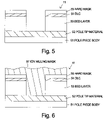
- FIG. 5 is a section of a wafer, perpendicular to the thin film surfaces, on which magnetic heads are being fabricated subsequent to FIG. 4 after the bed material has been etched away to form a trench according to an embodiment of the invention in preparation for fabricating the pole piece tip.
- FIG. 6 is a section of a wafer, perpendicular to the thin film surfaces, on which magnetic heads are being fabricated subsequent to FIG. 5 after the ion-milling mask material has been deposited in the trench according to an embodiment of the invention in preparation for fabricating the pole piece tip.
- FIG. 7A is a section of a wafer, perpendicular to the thin film surfaces, on which magnetic heads are being fabricated subsequent to FIG. 6 after a planarization process has removed the overfill of the ion-milling mask material and the hard mask material according to an embodiment of the invention in preparation for fabricating the pole piece tip.
- FIG. 7B is a section of a wafer, perpendicular to the thin film surfaces, on which magnetic heads are being fabricated subsequent to FIG. 6 after a wet etch process has removed the overfill of the ion-milling mask material according to an embodiment of the invention in preparation for fabricating the pole piece tip.
- FIG. 8 is a section of a wafer, perpendicular to the thin film surfaces, on which magnetic heads are being fabricated subsequent to FIG. 7 after an etching process has removed the bed material leaving the ion-milling mask according to an embodiment of the invention in preparation for fabricating the pole piece tip.
- FIG. 9 is a section of a wafer, perpendicular to the thin film surfaces, on which magnetic heads are being fabricated subsequent to FIG. 8 after an ion-milling process has removed the unmasked pole piece tip material leaving the pole piece tip according to an embodiment of the invention.
- FIG. 10 is an enlarged view of a beveled pole piece tip according to the invention as viewed from the air-bearing surface.
- the invention relates to the write head portion of the magnetic transducer and does not place limits on the type of read head that can be used with it.
- the read head portion of the transducer is fabricated first, but transducers with the write head portion fabricated first have been described in the prior art.
- a write head according to the invention may be fabricated before or after the read head portion of the transducer.
- FIG. 3 The section view is perpendicular to the surface of the thin films on wafer 11 .
- the ferromagnetic material for the body of the pole piece 51 has been deposited and patterned according to the prior art.
- One or more thin layers of ferromagnetic materials are deposited to provide the pole tip material 52 for the pole piece tip according to the prior art.
- the use of a different material and/or structure for the pole tip is advantageous for reasons outside of the scope of this invention. As one example, a higher moment material can be used.
- a laminated structure for the pole piece tip is also known in the art. The invention can be used with any type of pole piece tip structure.
- the thickness of the pole tip material 52 is according to the prior art and is not critical to the method of the invention, but for illustration purposes can be assumed to be on the order of 200 nm.
- the bed layer 53 is deposited onto the pole tip material 52 .
- the bed layer 53 will be used to form a void in which the ion-milling mask will be formed.
- the material for the bed layer is selected to allow a selective removal process which will leave the ion-milling mask material intact.
- the bed layer 53 can be hard bake or a dielectric material. Suitable dielectric materials include SiO 2 , SiON, Si x N y nitrides, and Al 2 O 3 .
- the thickness of the bed layer 53 determines the thickness of final ion milling mask as will be seen.
- the thickness needed will vary depending on the selected materials, the length of the ion-milling time, etc. and can be determined empirically. A value of one micron is reasonable value.
- the photoresist deposition and patterning can begin at this point, but the optional layers useful for CMP endpoint detection and mask resolution will be described.
- an optional thin layer of diamond-like carbon (DLC) 54 is deposited to serve as a CMP endpoint detection aid. As is known in the art the DLC detectably slows down the CMP process to provide an indicator of the progress of the planarization and allows the process to stopped at the desired point. Other materials useful for this purpose can be used.
- the method continues with the deposition of an optional hard mask material 55 such as NiFe.
- the hard mask improves the precision of the trench width since it can withstand the RIE better than the photoresist alone.
- the thickness of the hard mask material 55 can be determined empirically. A 30 nm thickness of NiFe is a reasonable value.
- the photoresist mask 56 is deposited onto the hard mask 55 and processed to form a void in the planar shape of the desired pole piece tip.
- the first underlying layer in the embodiment shown is the hard mask 55 .
- the bed layer 53 will be the first layer under the photoresist.
- the hard mask 55 is opened up at this point preferably by ion milling through the photoresist mask 56 .
- the resulting state of the wafer 11 is shown in FIG. 3 .
- Removal of the hard mask 55 leaves the DLC layer 54 exposed in the void.
- the DLC is preferably removed by a RIE process and then the photoresist 56 is stripped. The result is shown in FIG. 4 .
- the surface of the bed layer 53 is now exposed in the void.
- the preferred method for removing the bed layer material will depend on the particular material, but for SiO 2 , RIE is preferred.
- the result is shown in FIG. 5 .
- the void or trench now extends down to the surface of the pole tip material 52 and the wafer is ready for deposition of the ion-milling mask material.
- the ion-milling mask material is deposited over the wafer to overfill the trench.
- the result is shown in FIG. 6 .
- the wafer is then processed to remove the excess ion-milling mask material.
- a planarization process CMP
- CMP planarization process
- a wet etch process can be to remove the excess material while leaving the hard mask 55 .
- FIG. 7B The embodiment shown in FIG. 7B does not include the optional DLC layer 54 , since CMP is not used.
- the ion-milling mask 57 has been formed in the trench in the bed layer 53 .
- the material for the ion-milling mask 57 is selected for its ability to resist the ion-milling process.
- Alumina is preferable, but other resistant materials can be used such as, carbon.
- the ion-milling mask material can be deposited by any appropriate prior art means, but atomic layer deposition (ALD) or atomic layer chemical vapor deposition (ALCVD) is preferred.
- the trench which is the form for ion-milling mask should have a high aspect ratio. ALD or ALCVD is preferred for its ability to deposit materials in a deep high aspect ratio trench.
- the bed layer 53 is removed by a process which will leave the ion-milling mask 57 intact.
- a RIE process is preferred for an SiO 2 bed layer 53 and an alumina mask 57 . If a hard mask has been included and the wet etch option has been used, the hard mask 55 can still be present on the bed 53 .
- a suitable RIE, ash or wet etch process can be selected to remove both the hard mask 55 and the bed layer 53 . The result is shown in FIG. 8 .
- the wafer is now ready to use ion-milling to shape the pole piece tip. Ion-milling will remove all of the pole tip material 52 not protected by the ion-milling mask 57 as shown in FIG. 9 .
- the sides of the pole piece tip 52 T will be beveled inward since the ion-milling will remove material farther away from the ion-milling mask at a slightly higher rate. This inward beveling is desirable.
- the ion-milling should preferably by continued to remove some of the underlying pole body 51 to ensure complete removal of the unwanted pole tip material and to enhance the shape of the pole body by forming a slight bevel sloping away from the pole piece tip 52 T.
- the ion-milling process can be monitored using SEM imaging or by sampling using FIB cross-sectioning and then adjusted to improve the process.
- the ion-milling mask 57 does not to be removed.
- the area where the ion-milling mask 57 resides will be in the write gap which is typically a non-magnetic material such as alumina and, therefore, the alumina or similar material used for the mask will simply become part of the gap.
- the ion-milling mask 57 can also be removed after ion-milling so that it does not appear in the final head. After the ion-milling according to the invention the process of fabricating the head continues according to the prior art.
- the method of the invention can be used with head designs that require sawing and lapping as is the case for the head illustrated in FIG. 10 .
- the rest of the write head including the gap, coil and return pole piece 43 are completed and the saw cut is made along the plane of the air-bearing surface which is perpendicular to the thin film surface.
- a view of the 52 T as viewed from the air-bearing surface is illustrated in FIG. 10 .
- the ion-milling mask 57 has been left in place and resides in the write gap as described above.
- the ion-milling mask 57 can be the same material as used for the gap, for example, alumina, so the ion-milling mask 57 can blend in with the other material in the gap.
Abstract
Description
Claims (17)
Priority Applications (2)
| Application Number | Priority Date | Filing Date | Title |
|---|---|---|---|
| US10/882,883 US7186348B2 (en) | 2004-06-30 | 2004-06-30 | Method for fabricating a pole tip in a magnetic transducer |
| US11/707,524 US7742258B2 (en) | 2004-06-30 | 2007-02-12 | Magnetic transducer with milling mask |
Applications Claiming Priority (1)
| Application Number | Priority Date | Filing Date | Title |
|---|---|---|---|
| US10/882,883 US7186348B2 (en) | 2004-06-30 | 2004-06-30 | Method for fabricating a pole tip in a magnetic transducer |
Related Child Applications (1)
| Application Number | Title | Priority Date | Filing Date |
|---|---|---|---|
| US11/707,524 Division US7742258B2 (en) | 2004-06-30 | 2007-02-12 | Magnetic transducer with milling mask |
Publications (2)
| Publication Number | Publication Date |
|---|---|
| US20060000795A1 US20060000795A1 (en) | 2006-01-05 |
| US7186348B2 true US7186348B2 (en) | 2007-03-06 |
Family
ID=35512816
Family Applications (2)
| Application Number | Title | Priority Date | Filing Date |
|---|---|---|---|
| US10/882,883 Expired - Fee Related US7186348B2 (en) | 2004-06-30 | 2004-06-30 | Method for fabricating a pole tip in a magnetic transducer |
| US11/707,524 Expired - Fee Related US7742258B2 (en) | 2004-06-30 | 2007-02-12 | Magnetic transducer with milling mask |
Family Applications After (1)
| Application Number | Title | Priority Date | Filing Date |
|---|---|---|---|
| US11/707,524 Expired - Fee Related US7742258B2 (en) | 2004-06-30 | 2007-02-12 | Magnetic transducer with milling mask |
Country Status (1)
| Country | Link |
|---|---|
| US (2) | US7186348B2 (en) |
Cited By (20)
| Publication number | Priority date | Publication date | Assignee | Title |
|---|---|---|---|---|
| US20060172532A1 (en) * | 2005-01-11 | 2006-08-03 | Hitachi Global Storage Technologies Netherlands B.V. | Method of manufacturing a magnetic head |
| US20060171073A1 (en) * | 2002-08-19 | 2006-08-03 | Kiyoshi Kobayashi | Thin-film magnetic head for perpendicular magnetic recording |
| US20060215317A1 (en) * | 2005-03-24 | 2006-09-28 | Samsung Electronics Co., Ltd. | Magnetic recording head and method of manufacturing the same |
| US20070000861A1 (en) * | 2005-06-28 | 2007-01-04 | Kabushiki Kaisha Toshiba | Method and apparatus for manufacturing magnetic recording media |
| US20070245544A1 (en) * | 2006-04-25 | 2007-10-25 | Hitachi Global Storage Technologies Netherlands B.V. | Method for making a perpendicular magnetic recording write head |
| US20080151422A1 (en) * | 2006-12-22 | 2008-06-26 | Lille Jeffrey S | Enhanced planarization liftoff structure and method for making the same |
| US20080285174A1 (en) * | 2007-05-14 | 2008-11-20 | Kabushiki Kaisha Toshiba | Magnetic recording medium and magnetic storage device |
| US20090081482A1 (en) * | 2007-09-26 | 2009-03-26 | Kabushiki Kaisha Toshiba | Magnetic recording medium and method of manufacturing the same |
| US20090226760A1 (en) * | 2008-03-06 | 2009-09-10 | Christian Rene Bonhote | Inductive write head with slanted electroplated member and method for producing the same |
| US20090251821A1 (en) * | 2008-04-04 | 2009-10-08 | Seagate Technology Llc | Dedicated id-od writer with beveled pole tips and method of manufacture |
| US20090279206A1 (en) * | 2008-05-07 | 2009-11-12 | Seagate Technology Llc | Fabrication of trapezoidal pole for magnetic recording |
| US20100024201A1 (en) * | 2008-07-31 | 2010-02-04 | Quang Le | Method for fabricating narrow magnetic read width tmr/cpp sensors |
| US8468683B2 (en) | 2011-10-31 | 2013-06-25 | HGST Netherlands B.V. | High bevel angle magnetic writer pole fabrication process |
| US8607438B1 (en) | 2011-12-01 | 2013-12-17 | Western Digital (Fremont), Llc | Method for fabricating a read sensor for a read transducer |
| US8749790B1 (en) | 2011-12-08 | 2014-06-10 | Western Digital (Fremont), Llc | Structure and method to measure waveguide power absorption by surface plasmon element |
| US8790524B1 (en) | 2010-09-13 | 2014-07-29 | Western Digital (Fremont), Llc | Method and system for providing a magnetic recording transducer using a line hard mask and a wet-etchable mask |
| US8964333B1 (en) | 2010-05-28 | 2015-02-24 | Western Digital (Fremont), Llc | Energy assisted magnetic recording transducer having an electronic lapping guide corresponding to a near-field transducer |
| US9007719B1 (en) | 2013-10-23 | 2015-04-14 | Western Digital (Fremont), Llc | Systems and methods for using double mask techniques to achieve very small features |
| US9406331B1 (en) | 2013-06-17 | 2016-08-02 | Western Digital (Fremont), Llc | Method for making ultra-narrow read sensor and read transducer device resulting therefrom |
| US9441938B1 (en) | 2013-10-08 | 2016-09-13 | Western Digital (Fremont), Llc | Test structures for measuring near field transducer disc length |
Families Citing this family (9)
| Publication number | Priority date | Publication date | Assignee | Title |
|---|---|---|---|---|
| US7574536B2 (en) * | 2005-04-22 | 2009-08-11 | Sun Microsystems, Inc. | Routing direct memory access requests using doorbell addresses |
| US7241697B2 (en) * | 2005-07-07 | 2007-07-10 | Hitachi Global Storage Technologies Netherlands Bv | Method for sensor edge control and track width definition for narrow track width devices |
| US7429493B2 (en) * | 2005-07-18 | 2008-09-30 | Hitachi Global Storage Technologies Netherlands B.V. | Method for fabricating a magnetic head for perpendicular recording using a CMP lift-off and resistant layer |
| US8079135B1 (en) | 2007-12-13 | 2011-12-20 | Western Digital (Fremont), Llc | Method for providing a perpendicular magnetic recording (PMR) transducer |
| US20100084262A1 (en) * | 2008-10-02 | 2010-04-08 | Tdk Corporation | Manufacturing method of perpendicular magnetic recording head |
| US8432637B2 (en) | 2010-11-10 | 2013-04-30 | HGST Netherlands B.V. | Wet etching silicon oxide during the formation of a damascene pole and adjacent structure |
| EP2502877B1 (en) * | 2011-03-23 | 2013-10-02 | Patek Philippe SA Genève | Method for manufacturing a composite part, notably for a clock movement |
| US8506828B1 (en) * | 2011-06-28 | 2013-08-13 | Western Digital (Fremont), Llc | Method and system for providing a magnetic recording transducer using an ion beam scan polishing planarization |
| US11174167B1 (en) | 2020-08-18 | 2021-11-16 | Group14 Technologies, Inc. | Silicon carbon composites comprising ultra low Z |
Citations (22)
| Publication number | Priority date | Publication date | Assignee | Title |
|---|---|---|---|---|
| US5246884A (en) | 1991-10-30 | 1993-09-21 | International Business Machines Corporation | Cvd diamond or diamond-like carbon for chemical-mechanical polish etch stop |
| JP2000173987A (en) | 1998-12-01 | 2000-06-23 | Canon Sales Co Inc | Semiconductor device and formation of film for semiconductor device |
| US6111724A (en) * | 1998-04-10 | 2000-08-29 | International Business Machines Corporation | Method of making a magnetic write head with plated self-aligned zero throat height defining layer without reflective notching of a second pole tip |
| US6238582B1 (en) | 1999-03-30 | 2001-05-29 | Veeco Instruments, Inc. | Reactive ion beam etching method and a thin film head fabricated using the method |
| US20020017018A1 (en) * | 2000-06-02 | 2002-02-14 | Shigehisa Ohkawara | Manufacturing method of magneto-resistive effect type head |
| US20020036873A1 (en) | 2000-09-26 | 2002-03-28 | Kabushiki Kaisha Toshiba | Yoke type reproducing magnetic head, method for fabricating same, and magnetic disk unit |
| JP2002100011A (en) | 2000-09-26 | 2002-04-05 | Sony Corp | Magnetoresistance effect type magnetic head and method for producing the same |
| US20020080525A1 (en) * | 2000-12-26 | 2002-06-27 | Alps Electric Co., Ltd. | Perpendicular magnetic recording head including nonmagnetic layer overlaying main pole layer |
| US6558516B1 (en) * | 1999-12-09 | 2003-05-06 | Tdk Corporation | Method of frame plating and method of forming magnetic pole of thin-film magnetic head |
| US6586049B2 (en) * | 1997-08-28 | 2003-07-01 | Tdk Corporation | Patterning method using mask and manufacturing method for composite type thin film magnetic head using the patterning method |
| US20030137771A1 (en) | 1998-04-10 | 2003-07-24 | Emilio Santini Hugo Alberto | Method of making a write head with self-aligned pedestal shaped pole tips which are separated by a zero throat height defining layer |
| US6604275B1 (en) * | 1997-10-15 | 2003-08-12 | Tdk Corporation | Method of manufacturing thin-film magnetic head |
| US20030188422A1 (en) * | 1999-03-29 | 2003-10-09 | Kabushiki Kaisha Toshiba | Magnetic head manufacturing method |
| US20030193759A1 (en) | 1997-05-14 | 2003-10-16 | Tdk Corporation | Magnetoresistance effect device |
| US20030219980A1 (en) * | 2002-05-24 | 2003-11-27 | Tdk Corporation | Pattern forming method, method of making microdevice, method of making thin-film magnetic head, method of making magnetic head slider, method of making magnetic head apparatus, and method of making magnetic recording and reproducing apparatus |
| US20030223150A1 (en) | 2002-05-28 | 2003-12-04 | Lee Edward Hin Pong | Method of protecting the pole piece of a magnetic head during the ion mill patterning of the yoke |
| US6664026B2 (en) | 2001-03-22 | 2003-12-16 | International Business Machines Corporation | Method of manufacturing high aspect ratio photolithographic features |
| US20040027730A1 (en) | 2002-08-09 | 2004-02-12 | Lille Jeffrey Scott | Narrow track read sensor and method of making the same |
| US20040032692A1 (en) * | 2002-08-19 | 2004-02-19 | Alps Electric Co., Ltd. | Thin-film magnetic head for perpendicular magnetic recording |
| US20040168302A1 (en) * | 1997-10-15 | 2004-09-02 | Tdk Corporation | Method for manufacturing thin-film magnetic head |
| US20050068665A1 (en) * | 2003-09-26 | 2005-03-31 | Hitachi Global Storage Technologies | Write pole fabrication for perpendicular recording |
| US20050175864A1 (en) * | 2002-12-18 | 2005-08-11 | Fujitsu Limited | Magnetic thin film and magnetic head using the same |
Family Cites Families (9)
| Publication number | Priority date | Publication date | Assignee | Title |
|---|---|---|---|---|
| US2002A (en) * | 1841-03-12 | Tor and planter for plowing | ||
| US2003A (en) * | 1841-03-12 | Improvement in horizontal windivhlls | ||
| US6301076B1 (en) * | 1998-03-20 | 2001-10-09 | Seagate Technology Llc | Narrow track inductive write head having a two-piece pole |
| JP3677423B2 (en) * | 1999-12-28 | 2005-08-03 | 株式会社東芝 | Thermally assisted magnetic recording method and thermally assisted magnetic recording apparatus |
| US7128732B2 (en) * | 2000-07-03 | 2006-10-31 | Kimberly-Clark Worldwide, Inc. | Undergarment protection article and method |
| US7441325B2 (en) * | 2004-04-30 | 2008-10-28 | Hitachi Global Storage Technologies Netherlands B.V. | Perpendicular head with trailing shield and rhodium gap process |
| US7307815B2 (en) * | 2004-05-19 | 2007-12-11 | Headway Technologies, Inc. | Method for making a perpendicular magnetic recording write head with a self aligned stitched write shield |
| US7672079B2 (en) * | 2004-07-07 | 2010-03-02 | Headway Technologies, Inc. | Pole width control on plated bevel main pole design of a perpendicular magnetic recording head |
| KR100718146B1 (en) * | 2006-01-13 | 2007-05-14 | 삼성전자주식회사 | Heat assisted magnetic recording head |
-
2004
- 2004-06-30 US US10/882,883 patent/US7186348B2/en not_active Expired - Fee Related
-
2007
- 2007-02-12 US US11/707,524 patent/US7742258B2/en not_active Expired - Fee Related
Patent Citations (22)
| Publication number | Priority date | Publication date | Assignee | Title |
|---|---|---|---|---|
| US5246884A (en) | 1991-10-30 | 1993-09-21 | International Business Machines Corporation | Cvd diamond or diamond-like carbon for chemical-mechanical polish etch stop |
| US20030193759A1 (en) | 1997-05-14 | 2003-10-16 | Tdk Corporation | Magnetoresistance effect device |
| US6586049B2 (en) * | 1997-08-28 | 2003-07-01 | Tdk Corporation | Patterning method using mask and manufacturing method for composite type thin film magnetic head using the patterning method |
| US20040168302A1 (en) * | 1997-10-15 | 2004-09-02 | Tdk Corporation | Method for manufacturing thin-film magnetic head |
| US6604275B1 (en) * | 1997-10-15 | 2003-08-12 | Tdk Corporation | Method of manufacturing thin-film magnetic head |
| US6111724A (en) * | 1998-04-10 | 2000-08-29 | International Business Machines Corporation | Method of making a magnetic write head with plated self-aligned zero throat height defining layer without reflective notching of a second pole tip |
| US20030137771A1 (en) | 1998-04-10 | 2003-07-24 | Emilio Santini Hugo Alberto | Method of making a write head with self-aligned pedestal shaped pole tips which are separated by a zero throat height defining layer |
| JP2000173987A (en) | 1998-12-01 | 2000-06-23 | Canon Sales Co Inc | Semiconductor device and formation of film for semiconductor device |
| US20030188422A1 (en) * | 1999-03-29 | 2003-10-09 | Kabushiki Kaisha Toshiba | Magnetic head manufacturing method |
| US6238582B1 (en) | 1999-03-30 | 2001-05-29 | Veeco Instruments, Inc. | Reactive ion beam etching method and a thin film head fabricated using the method |
| US6558516B1 (en) * | 1999-12-09 | 2003-05-06 | Tdk Corporation | Method of frame plating and method of forming magnetic pole of thin-film magnetic head |
| US20020017018A1 (en) * | 2000-06-02 | 2002-02-14 | Shigehisa Ohkawara | Manufacturing method of magneto-resistive effect type head |
| US20020036873A1 (en) | 2000-09-26 | 2002-03-28 | Kabushiki Kaisha Toshiba | Yoke type reproducing magnetic head, method for fabricating same, and magnetic disk unit |
| JP2002100011A (en) | 2000-09-26 | 2002-04-05 | Sony Corp | Magnetoresistance effect type magnetic head and method for producing the same |
| US20020080525A1 (en) * | 2000-12-26 | 2002-06-27 | Alps Electric Co., Ltd. | Perpendicular magnetic recording head including nonmagnetic layer overlaying main pole layer |
| US6664026B2 (en) | 2001-03-22 | 2003-12-16 | International Business Machines Corporation | Method of manufacturing high aspect ratio photolithographic features |
| US20030219980A1 (en) * | 2002-05-24 | 2003-11-27 | Tdk Corporation | Pattern forming method, method of making microdevice, method of making thin-film magnetic head, method of making magnetic head slider, method of making magnetic head apparatus, and method of making magnetic recording and reproducing apparatus |
| US20030223150A1 (en) | 2002-05-28 | 2003-12-04 | Lee Edward Hin Pong | Method of protecting the pole piece of a magnetic head during the ion mill patterning of the yoke |
| US20040027730A1 (en) | 2002-08-09 | 2004-02-12 | Lille Jeffrey Scott | Narrow track read sensor and method of making the same |
| US20040032692A1 (en) * | 2002-08-19 | 2004-02-19 | Alps Electric Co., Ltd. | Thin-film magnetic head for perpendicular magnetic recording |
| US20050175864A1 (en) * | 2002-12-18 | 2005-08-11 | Fujitsu Limited | Magnetic thin film and magnetic head using the same |
| US20050068665A1 (en) * | 2003-09-26 | 2005-03-31 | Hitachi Global Storage Technologies | Write pole fabrication for perpendicular recording |
Cited By (36)
| Publication number | Priority date | Publication date | Assignee | Title |
|---|---|---|---|---|
| US20060171073A1 (en) * | 2002-08-19 | 2006-08-03 | Kiyoshi Kobayashi | Thin-film magnetic head for perpendicular magnetic recording |
| US7312952B2 (en) * | 2002-08-19 | 2007-12-25 | Alps Electric Co., Ltd. | Thin-film magnetic head for perpendicular magnetic recording |
| US7605006B2 (en) * | 2005-01-11 | 2009-10-20 | Hitachi Global Storage Technologies Netherlands B.V. | Method of manufacturing a magnetic head |
| US20060172532A1 (en) * | 2005-01-11 | 2006-08-03 | Hitachi Global Storage Technologies Netherlands B.V. | Method of manufacturing a magnetic head |
| US7602584B2 (en) * | 2005-03-24 | 2009-10-13 | Samsung Electronics Co., Ltd. | Magnetic recording head with trapezoidal layered portion and method of manufacturing the same |
| US20060215317A1 (en) * | 2005-03-24 | 2006-09-28 | Samsung Electronics Co., Ltd. | Magnetic recording head and method of manufacturing the same |
| US20070000861A1 (en) * | 2005-06-28 | 2007-01-04 | Kabushiki Kaisha Toshiba | Method and apparatus for manufacturing magnetic recording media |
| US8221637B2 (en) | 2005-06-28 | 2012-07-17 | Kabushiki Kaisha Toshiba | Method and apparatus for manufacturing magnetic recording media |
| US20100264019A1 (en) * | 2005-06-28 | 2010-10-21 | Kabushiki Kaisha Toshiba | Method and apparatus for manufacturing magnetic recording media |
| US7771602B2 (en) * | 2005-06-28 | 2010-08-10 | Kabushiki Kaisha Toshiba | Method and apparatus for manufacturing magnetic recording media |
| US7509729B2 (en) * | 2006-04-25 | 2009-03-31 | Hitachi Global Storage Technologies Netherlands B.V. | Method for making a perpendicular magnetic recording write head |
| US20070245544A1 (en) * | 2006-04-25 | 2007-10-25 | Hitachi Global Storage Technologies Netherlands B.V. | Method for making a perpendicular magnetic recording write head |
| US7813080B2 (en) * | 2006-12-22 | 2010-10-12 | Hitachi Global Storage Technologies Netherlands B.V. | Enhanced planarization liftoff structure and method for making the same |
| US20080151422A1 (en) * | 2006-12-22 | 2008-06-26 | Lille Jeffrey S | Enhanced planarization liftoff structure and method for making the same |
| US20080285174A1 (en) * | 2007-05-14 | 2008-11-20 | Kabushiki Kaisha Toshiba | Magnetic recording medium and magnetic storage device |
| US8049993B2 (en) | 2007-05-14 | 2011-11-01 | Kabushiki Kaisha Toshiba | Magnetic recording medium and magnetic storage device |
| US20090081482A1 (en) * | 2007-09-26 | 2009-03-26 | Kabushiki Kaisha Toshiba | Magnetic recording medium and method of manufacturing the same |
| US8652338B2 (en) | 2007-09-26 | 2014-02-18 | Kabushiki Kaisha Toshiba | Magnetic recording medium and method of manufacturing the same |
| US8338007B2 (en) | 2007-09-26 | 2012-12-25 | Kabushiki Kaisha Toshiba | Magnetic recording medium and magnetic recording apparatus |
| US20090226760A1 (en) * | 2008-03-06 | 2009-09-10 | Christian Rene Bonhote | Inductive write head with slanted electroplated member and method for producing the same |
| US8028400B2 (en) | 2008-03-06 | 2011-10-04 | Hitachi Global Storage Technologies Netherlands B.V. | Method for manufacturing a magnetic write head |
| US20090251821A1 (en) * | 2008-04-04 | 2009-10-08 | Seagate Technology Llc | Dedicated id-od writer with beveled pole tips and method of manufacture |
| US8310782B2 (en) | 2008-04-04 | 2012-11-13 | Seagate Technology Llc | Dedicated ID-OD writer with beveled pole tips and method of manufacture |
| US8259411B2 (en) | 2008-05-07 | 2012-09-04 | Seagate Technology Llc | Fabrication of trapezoidal pole for magnetic recording |
| US20090279206A1 (en) * | 2008-05-07 | 2009-11-12 | Seagate Technology Llc | Fabrication of trapezoidal pole for magnetic recording |
| US8848315B2 (en) | 2008-05-07 | 2014-09-30 | Seagate Technology Llc | Pole for magnetic recording |
| US8011084B2 (en) | 2008-07-31 | 2011-09-06 | Hitachi Global Storage Technologies Netherlands B.V. | Method for fabricating narrow magnetic read width TMR/CPP sensors |
| US20100024201A1 (en) * | 2008-07-31 | 2010-02-04 | Quang Le | Method for fabricating narrow magnetic read width tmr/cpp sensors |
| US8964333B1 (en) | 2010-05-28 | 2015-02-24 | Western Digital (Fremont), Llc | Energy assisted magnetic recording transducer having an electronic lapping guide corresponding to a near-field transducer |
| US8790524B1 (en) | 2010-09-13 | 2014-07-29 | Western Digital (Fremont), Llc | Method and system for providing a magnetic recording transducer using a line hard mask and a wet-etchable mask |
| US8468683B2 (en) | 2011-10-31 | 2013-06-25 | HGST Netherlands B.V. | High bevel angle magnetic writer pole fabrication process |
| US8607438B1 (en) | 2011-12-01 | 2013-12-17 | Western Digital (Fremont), Llc | Method for fabricating a read sensor for a read transducer |
| US8749790B1 (en) | 2011-12-08 | 2014-06-10 | Western Digital (Fremont), Llc | Structure and method to measure waveguide power absorption by surface plasmon element |
| US9406331B1 (en) | 2013-06-17 | 2016-08-02 | Western Digital (Fremont), Llc | Method for making ultra-narrow read sensor and read transducer device resulting therefrom |
| US9441938B1 (en) | 2013-10-08 | 2016-09-13 | Western Digital (Fremont), Llc | Test structures for measuring near field transducer disc length |
| US9007719B1 (en) | 2013-10-23 | 2015-04-14 | Western Digital (Fremont), Llc | Systems and methods for using double mask techniques to achieve very small features |
Also Published As
| Publication number | Publication date |
|---|---|
| US20070139816A1 (en) | 2007-06-21 |
| US20060000795A1 (en) | 2006-01-05 |
| US7742258B2 (en) | 2010-06-22 |
Similar Documents
| Publication | Publication Date | Title |
|---|---|---|
| US7742258B2 (en) | Magnetic transducer with milling mask | |
| US8079135B1 (en) | Method for providing a perpendicular magnetic recording (PMR) transducer | |
| US7367112B2 (en) | Method of fabricating a head for perpendicular magnetic recording with a self-aligning side shield structure | |
| US8879207B1 (en) | Method for providing a side shield for a magnetic recording transducer using an air bridge | |
| US8844120B1 (en) | Method for providing a magnetic recording transducer including an assist pole having surfaces angled with respect to the ABS | |
| US8797680B1 (en) | Perpendicular magnetic recording head having reduced shield notching | |
| US8576517B1 (en) | Magnetic recording transducer having side shields between the coils and the air-bearing surface | |
| US7377024B2 (en) | Method of making a magnetic write head with trailing shield throat pad | |
| US8334093B2 (en) | Method and system for providing a perpendicular magnetic recording head | |
| US8262919B1 (en) | Method and system for providing a perpendicular magnetic recording pole using multiple chemical mechanical planarizations | |
| US8231796B1 (en) | Method and system for providing a magnetic recording transducer having side shields | |
| US8125732B2 (en) | Tapered PMR write pole with straight side wall portion | |
| US7757380B2 (en) | Methods for the manufacture of notched trailing shields | |
| US7429493B2 (en) | Method for fabricating a magnetic head for perpendicular recording using a CMP lift-off and resistant layer | |
| US7124498B2 (en) | Method for manufacturing magnetic head | |
| US6524491B1 (en) | Double plate-up process for fabrication of composite magnetoresistive shared poles | |
| US8508886B2 (en) | Use of magnetic material for RIE stop layer during damascene main pole formation | |
| US7181828B2 (en) | Method for manufacturing perpendicular magnetic recording head | |
| US8914969B1 (en) | Method for providing a monolithic shield for a magnetic recording transducer | |
| JP4846773B2 (en) | Thin film magnetic head | |
| JPH10302219A (en) | Thin film magnetic head and production thereof | |
| JP2009099184A (en) | Perpendicular magnetic recording head and manufacturing method therefor | |
| US6900963B1 (en) | Thin film magnetic head with track width restricting groove formed to fully reach lower core layer, and manufacturing method for the same | |
| JP4183606B2 (en) | Manufacturing method of magnetic head | |
| US7770283B2 (en) | Method of fabricating a magnetic head |
Legal Events
| Date | Code | Title | Description |
|---|---|---|---|
| AS | Assignment |
Owner name: HITACHI GLOBAL STORAGE TECHNOLOGIES NETHERLANDS, B Free format text: ASSIGNMENT OF ASSIGNORS INTEREST;ASSIGNORS:CHEN, TSUNG YUAN;DRUIST, DAVID PATRICK;LE, QUANG;AND OTHERS;REEL/FRAME:015837/0032;SIGNING DATES FROM 20040628 TO 20040630 |
|
| FEPP | Fee payment procedure |
Free format text: PAYOR NUMBER ASSIGNED (ORIGINAL EVENT CODE: ASPN); ENTITY STATUS OF PATENT OWNER: LARGE ENTITY |
|
| STCF | Information on status: patent grant |
Free format text: PATENTED CASE |
|
| FEPP | Fee payment procedure |
Free format text: PAYER NUMBER DE-ASSIGNED (ORIGINAL EVENT CODE: RMPN); ENTITY STATUS OF PATENT OWNER: LARGE ENTITY Free format text: PAYOR NUMBER ASSIGNED (ORIGINAL EVENT CODE: ASPN); ENTITY STATUS OF PATENT OWNER: LARGE ENTITY |
|
| FPAY | Fee payment |
Year of fee payment: 4 |
|
| AS | Assignment |
Owner name: HGST, NETHERLANDS B.V., NETHERLANDS Free format text: CHANGE OF NAME;ASSIGNOR:HGST, NETHERLANDS B.V.;REEL/FRAME:029341/0777 Effective date: 20120723 Owner name: HGST NETHERLANDS B.V., NETHERLANDS Free format text: CHANGE OF NAME;ASSIGNOR:HITACHI GLOBAL STORAGE TECHNOLOGIES NETHERLANDS B.V.;REEL/FRAME:029341/0777 Effective date: 20120723 |
|
| FPAY | Fee payment |
Year of fee payment: 8 |
|
| AS | Assignment |
Owner name: WESTERN DIGITAL TECHNOLOGIES, INC., CALIFORNIA Free format text: ASSIGNMENT OF ASSIGNORS INTEREST;ASSIGNOR:HGST NETHERLANDS B.V.;REEL/FRAME:040819/0450 Effective date: 20160831 |
|
| FEPP | Fee payment procedure |
Free format text: MAINTENANCE FEE REMINDER MAILED (ORIGINAL EVENT CODE: REM.); ENTITY STATUS OF PATENT OWNER: LARGE ENTITY |
|
| LAPS | Lapse for failure to pay maintenance fees |
Free format text: PATENT EXPIRED FOR FAILURE TO PAY MAINTENANCE FEES (ORIGINAL EVENT CODE: EXP.); ENTITY STATUS OF PATENT OWNER: LARGE ENTITY |
|
| STCH | Information on status: patent discontinuation |
Free format text: PATENT EXPIRED DUE TO NONPAYMENT OF MAINTENANCE FEES UNDER 37 CFR 1.362 |
|
| FP | Lapsed due to failure to pay maintenance fee |
Effective date: 20190306 |