US7221046B2 - System to control effective series resistance of power delivery circuit - Google Patents
System to control effective series resistance of power delivery circuit Download PDFInfo
- Publication number
- US7221046B2 US7221046B2 US10/970,237 US97023704A US7221046B2 US 7221046 B2 US7221046 B2 US 7221046B2 US 97023704 A US97023704 A US 97023704A US 7221046 B2 US7221046 B2 US 7221046B2
- Authority
- US
- United States
- Prior art keywords
- portions
- resistive portions
- resistive
- integrated circuit
- coupled
- Prior art date
- Legal status (The legal status is an assumption and is not a legal conclusion. Google has not performed a legal analysis and makes no representation as to the accuracy of the status listed.)
- Expired - Fee Related, expires
Links
- 239000003990 capacitor Substances 0.000 claims abstract description 47
- 230000008878 coupling Effects 0.000 claims description 17
- 238000010168 coupling process Methods 0.000 claims description 17
- 238000005859 coupling reaction Methods 0.000 claims description 17
- 238000000034 method Methods 0.000 claims description 12
- 239000002861 polymer material Substances 0.000 claims 10
- 239000000463 material Substances 0.000 description 5
- 239000000758 substrate Substances 0.000 description 4
- 230000005540 biological transmission Effects 0.000 description 2
- 238000010586 diagram Methods 0.000 description 2
- 238000004519 manufacturing process Methods 0.000 description 2
- 229920000642 polymer Polymers 0.000 description 2
- 229910000679 solder Inorganic materials 0.000 description 2
- RYGMFSIKBFXOCR-UHFFFAOYSA-N Copper Chemical compound [Cu] RYGMFSIKBFXOCR-UHFFFAOYSA-N 0.000 description 1
- 239000004593 Epoxy Substances 0.000 description 1
- XUIMIQQOPSSXEZ-UHFFFAOYSA-N Silicon Chemical compound [Si] XUIMIQQOPSSXEZ-UHFFFAOYSA-N 0.000 description 1
- 230000004075 alteration Effects 0.000 description 1
- 239000000919 ceramic Substances 0.000 description 1
- 229920001940 conductive polymer Polymers 0.000 description 1
- 239000004020 conductor Substances 0.000 description 1
- 229910052802 copper Inorganic materials 0.000 description 1
- 239000010949 copper Substances 0.000 description 1
- 238000005516 engineering process Methods 0.000 description 1
- 230000001747 exhibiting effect Effects 0.000 description 1
- 230000006870 function Effects 0.000 description 1
- PCHJSUWPFVWCPO-UHFFFAOYSA-N gold Chemical compound [Au] PCHJSUWPFVWCPO-UHFFFAOYSA-N 0.000 description 1
- 229910052737 gold Inorganic materials 0.000 description 1
- 239000010931 gold Substances 0.000 description 1
- 238000012986 modification Methods 0.000 description 1
- 230000004048 modification Effects 0.000 description 1
- 238000004806 packaging method and process Methods 0.000 description 1
- 229910052710 silicon Inorganic materials 0.000 description 1
- 239000010703 silicon Substances 0.000 description 1
Images


Classifications
-
- H—ELECTRICITY
- H01—ELECTRIC ELEMENTS
- H01L—SEMICONDUCTOR DEVICES NOT COVERED BY CLASS H10
- H01L23/00—Details of semiconductor or other solid state devices
- H01L23/48—Arrangements for conducting electric current to or from the solid state body in operation, e.g. leads, terminal arrangements ; Selection of materials therefor
- H01L23/50—Arrangements for conducting electric current to or from the solid state body in operation, e.g. leads, terminal arrangements ; Selection of materials therefor for integrated circuit devices, e.g. power bus, number of leads
-
- H—ELECTRICITY
- H01—ELECTRIC ELEMENTS
- H01L—SEMICONDUCTOR DEVICES NOT COVERED BY CLASS H10
- H01L23/00—Details of semiconductor or other solid state devices
- H01L23/52—Arrangements for conducting electric current within the device in operation from one component to another, i.e. interconnections, e.g. wires, lead frames
- H01L23/538—Arrangements for conducting electric current within the device in operation from one component to another, i.e. interconnections, e.g. wires, lead frames the interconnection structure between a plurality of semiconductor chips being formed on, or in, insulating substrates
- H01L23/5386—Geometry or layout of the interconnection structure
-
- H—ELECTRICITY
- H01—ELECTRIC ELEMENTS
- H01L—SEMICONDUCTOR DEVICES NOT COVERED BY CLASS H10
- H01L24/00—Arrangements for connecting or disconnecting semiconductor or solid-state bodies; Methods or apparatus related thereto
- H01L24/01—Means for bonding being attached to, or being formed on, the surface to be connected, e.g. chip-to-package, die-attach, "first-level" interconnects; Manufacturing methods related thereto
- H01L24/10—Bump connectors ; Manufacturing methods related thereto
- H01L24/15—Structure, shape, material or disposition of the bump connectors after the connecting process
- H01L24/17—Structure, shape, material or disposition of the bump connectors after the connecting process of a plurality of bump connectors
-
- H—ELECTRICITY
- H01—ELECTRIC ELEMENTS
- H01L—SEMICONDUCTOR DEVICES NOT COVERED BY CLASS H10
- H01L2224/00—Indexing scheme for arrangements for connecting or disconnecting semiconductor or solid-state bodies and methods related thereto as covered by H01L24/00
- H01L2224/01—Means for bonding being attached to, or being formed on, the surface to be connected, e.g. chip-to-package, die-attach, "first-level" interconnects; Manufacturing methods related thereto
- H01L2224/10—Bump connectors; Manufacturing methods related thereto
- H01L2224/15—Structure, shape, material or disposition of the bump connectors after the connecting process
- H01L2224/16—Structure, shape, material or disposition of the bump connectors after the connecting process of an individual bump connector
- H01L2224/161—Disposition
- H01L2224/16151—Disposition the bump connector connecting between a semiconductor or solid-state body and an item not being a semiconductor or solid-state body, e.g. chip-to-substrate, chip-to-passive
- H01L2224/16221—Disposition the bump connector connecting between a semiconductor or solid-state body and an item not being a semiconductor or solid-state body, e.g. chip-to-substrate, chip-to-passive the body and the item being stacked
- H01L2224/16225—Disposition the bump connector connecting between a semiconductor or solid-state body and an item not being a semiconductor or solid-state body, e.g. chip-to-substrate, chip-to-passive the body and the item being stacked the item being non-metallic, e.g. insulating substrate with or without metallisation
-
- H—ELECTRICITY
- H01—ELECTRIC ELEMENTS
- H01L—SEMICONDUCTOR DEVICES NOT COVERED BY CLASS H10
- H01L2924/00—Indexing scheme for arrangements or methods for connecting or disconnecting semiconductor or solid-state bodies as covered by H01L24/00
- H01L2924/0001—Technical content checked by a classifier
- H01L2924/00011—Not relevant to the scope of the group, the symbol of which is combined with the symbol of this group
-
- H—ELECTRICITY
- H01—ELECTRIC ELEMENTS
- H01L—SEMICONDUCTOR DEVICES NOT COVERED BY CLASS H10
- H01L2924/00—Indexing scheme for arrangements or methods for connecting or disconnecting semiconductor or solid-state bodies as covered by H01L24/00
- H01L2924/0001—Technical content checked by a classifier
- H01L2924/00014—Technical content checked by a classifier the subject-matter covered by the group, the symbol of which is combined with the symbol of this group, being disclosed without further technical details
-
- H—ELECTRICITY
- H01—ELECTRIC ELEMENTS
- H01L—SEMICONDUCTOR DEVICES NOT COVERED BY CLASS H10
- H01L2924/00—Indexing scheme for arrangements or methods for connecting or disconnecting semiconductor or solid-state bodies as covered by H01L24/00
- H01L2924/01—Chemical elements
- H01L2924/01029—Copper [Cu]
-
- H—ELECTRICITY
- H01—ELECTRIC ELEMENTS
- H01L—SEMICONDUCTOR DEVICES NOT COVERED BY CLASS H10
- H01L2924/00—Indexing scheme for arrangements or methods for connecting or disconnecting semiconductor or solid-state bodies as covered by H01L24/00
- H01L2924/01—Chemical elements
- H01L2924/01079—Gold [Au]
-
- H—ELECTRICITY
- H01—ELECTRIC ELEMENTS
- H01L—SEMICONDUCTOR DEVICES NOT COVERED BY CLASS H10
- H01L2924/00—Indexing scheme for arrangements or methods for connecting or disconnecting semiconductor or solid-state bodies as covered by H01L24/00
- H01L2924/10—Details of semiconductor or other solid state devices to be connected
- H01L2924/11—Device type
- H01L2924/14—Integrated circuits
-
- H—ELECTRICITY
- H01—ELECTRIC ELEMENTS
- H01L—SEMICONDUCTOR DEVICES NOT COVERED BY CLASS H10
- H01L2924/00—Indexing scheme for arrangements or methods for connecting or disconnecting semiconductor or solid-state bodies as covered by H01L24/00
- H01L2924/15—Details of package parts other than the semiconductor or other solid state devices to be connected
- H01L2924/151—Die mounting substrate
- H01L2924/153—Connection portion
- H01L2924/1531—Connection portion the connection portion being formed only on the surface of the substrate opposite to the die mounting surface
- H01L2924/15312—Connection portion the connection portion being formed only on the surface of the substrate opposite to the die mounting surface being a pin array, e.g. PGA
-
- H—ELECTRICITY
- H01—ELECTRIC ELEMENTS
- H01L—SEMICONDUCTOR DEVICES NOT COVERED BY CLASS H10
- H01L2924/00—Indexing scheme for arrangements or methods for connecting or disconnecting semiconductor or solid-state bodies as covered by H01L24/00
- H01L2924/19—Details of hybrid assemblies other than the semiconductor or other solid state devices to be connected
- H01L2924/191—Disposition
- H01L2924/19101—Disposition of discrete passive components
- H01L2924/19106—Disposition of discrete passive components in a mirrored arrangement on two different side of a common die mounting substrate
-
- H—ELECTRICITY
- H05—ELECTRIC TECHNIQUES NOT OTHERWISE PROVIDED FOR
- H05K—PRINTED CIRCUITS; CASINGS OR CONSTRUCTIONAL DETAILS OF ELECTRIC APPARATUS; MANUFACTURE OF ASSEMBLAGES OF ELECTRICAL COMPONENTS
- H05K1/00—Printed circuits
- H05K1/02—Details
- H05K1/0213—Electrical arrangements not otherwise provided for
- H05K1/0216—Reduction of cross-talk, noise or electromagnetic interference
- H05K1/023—Reduction of cross-talk, noise or electromagnetic interference using auxiliary mounted passive components or auxiliary substances
- H05K1/0231—Capacitors or dielectric substances
-
- H—ELECTRICITY
- H05—ELECTRIC TECHNIQUES NOT OTHERWISE PROVIDED FOR
- H05K—PRINTED CIRCUITS; CASINGS OR CONSTRUCTIONAL DETAILS OF ELECTRIC APPARATUS; MANUFACTURE OF ASSEMBLAGES OF ELECTRICAL COMPONENTS
- H05K1/00—Printed circuits
- H05K1/16—Printed circuits incorporating printed electric components, e.g. printed resistor, capacitor, inductor
- H05K1/167—Printed circuits incorporating printed electric components, e.g. printed resistor, capacitor, inductor incorporating printed resistors
Definitions
- An integrated circuit package may provide physical protection to an integrated circuit die, dissipate heat generated by the integrated circuit die, and electrically connect the integrated circuit die to external circuitry.
- a conventional integrated circuit package may provide power and ground planes for distributing and routing power signals between the integrated circuit die and a motherboard. The transmission of these signals often results in unwanted resonance between the motherboard and the integrated circuit package, which may negatively affect the performance of the integrated circuit die.
- FIG. 1 is a cutaway side elevation of a system according to some embodiments.
- FIG. 2 is a top view of an element comprising a plurality of resistive portions according to some embodiments.
- FIG. 3 is a flow diagram of a method according to some embodiments.
- FIG. 4 includes a cutaway view of a capacitor and a perspective view of an element comprising a plurality of resistive portions according to some embodiments.
- FIG. 5 is a bottom view of an integrated circuit package according to some embodiments.
- FIG. 6 is a bottom view of an integrated circuit package having capacitors coupled thereto according to some embodiments.
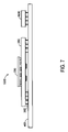
- FIG. 7 is a cutaway side elevation of a system according to some embodiments.
- FIG. 1 is a side elevation of system 100 according to some embodiments.
- System 100 includes integrated circuit die 200 , integrated circuit package 300 , and motherboard 400 .
- Integrated circuit die 200 may be fabricated using any suitable substrate material and fabrication technique and may provide any functions to system 100 .
- integrated circuit die 200 is a microprocessor die having a silicon substrate.
- Integrated circuit package 300 may comprise any ceramic, organic, and/or other suitable material.
- Package 300 is electrically coupled to circuit elements of die 200 by Controlled Collapse Chip Connect (C4) solder bumps 250 .
- C4 Controlled Collapse Chip Connect
- integrated circuit package 300 is electrically coupled to circuit 200 via wirebonds.
- Decoupling capacitors 310 through 340 are coupled to integrated circuit package 300 . Disposed between capacitors 310 through 340 are respective ones of elements 315 , 325 , 335 and 345 . As will be described in detail below, resistive portions of each of elements 315 , 325 , 335 and 345 are coupled to respective capacitor pads of capacitors 310 through 340 and to respective conductive contacts of integrated circuit package 300 . Such an arrangement may provide control over the equivalent series resistance of each of capacitors 310 through 340 . Some embodiments of the foregoing may reduce resonance between package 300 and motherboard 400 more effectively and/or more efficiently than conventional systems.
- Pins 350 couple package 300 to motherboard 400 .
- Pins 350 may carry power and other electrical signals between motherboard 400 and die 200 .
- pins 350 interface with a socket (not shown) of motherboard 400 .
- integrated circuit package 300 is a surface-mountable substrate such as an Organic Land Grid Array substrate that may be mounted directly on motherboard 400 or mounted on a pinned interposer which mates with a socket of motherboard 400 .
- Packaging systems other than those mentioned above may be used in conjunction with some embodiments.
- FIG. 2 is a top view of resistive element 500 according to some embodiments.
- Element 500 may represent one or more of elements 315 , 325 , 335 and 345 of FIG. 1 .
- Element 500 comprises resistive portions 501 through 510 and substantially non-conductive portion 520 .
- Portion 520 electrically isolates each of resistive portions 501 through 510 from each other of resistive portions 501 through 510 .
- Resistive portions 510 through 510 may comprise and material exhibiting a resistance that is suitable for the particular application in which element 500 is to be employed.
- substantially non-conductive portion 520 may comprise any one or more materials that are substantially non-conductive in view of the voltage and current levels of the particular application.
- resistive portions 501 through 510 comprise a resistive polymer and portion 520 also comprises a polymer. Such embodiments may facilitate the manufacturing of element 500 .
- element 500 may be manufactured as a sheet of non-conductive polymer. The sheet may be treated at locations corresponding to the locations of portions 501 through 510 in order to produce a material having an appropriate resistivity at the locations. Many elements 500 may be manufactured on a single sheet and then separated.
- the dashed arrows of FIG. 2 illustrate current flow between resistive portions 501 through 510 .
- Current may flow as indicated in a case that element 500 is coupled to pads of a capacitor and to conductive contacts of an integrated circuit package as described below.
- the number, location and size of resistive portions 501 through 510 is not limited to that shown in FIG. 2 .
- the number, size and location, as well as the shape of element 500 may vary to correspond to the pads of the capacitor and the conductive contacts of the integrated circuit package to which element 500 is to be coupled.
- the composition and dimensions of each of resistive portions 501 through 510 may be controlled to provide a desired equivalent series resistance to the circuit to which element 500 is to be coupled.
- FIG. 3 is a flow diagram of a method according to some embodiments.
- Method 600 may be executed by any combination of hardware, software and/or firmware, and some or all of method 600 may be performed manually. Portions of method 600 may be performed by different entities. For example, method 600 may be performed by any combination of an integrated circuit manufacturer, a capacitor manufacturer, and a system integrator.
- FIG. 4 illustrates some embodiments of 601 .
- FIG. 4 includes a perspective view of element 500 and a cutaway perspective view of interdigitated capacitor 700 .
- Capacitor 700 comprises several positive and negative terminal plates that are alternately stacked and separated by a dielectric. The negative plates are electrically coupled to negative capacitor pads 711 , 713 , 715 (not shown), 717 and 719 , while the positive plates are electrically coupled to positive capacitor pads 712 , 714 , 716 (not shown), 718 and 720 . This arrangement may provide a lower equivalent series inductance than other arrangements.
- Element 500 may be placed on capacitor 700 at 601 so as to align each of resistive portions 501 through 510 to a respective one of pads 711 through 720 .
- Element 500 may be bonded to capacitor 700 using any suitable system that is or becomes known. Bonding element 500 to capacitor 700 may include bonding each of resistive portions 501 through 510 to the respective one of pads 711 through 720 and/or bonding substantially non-conductive portion 520 to body 730 of capacitor 700 . Other types of capacitors including two terminal, non-interdigitated capacitors may be used in conjunction with some embodiments. As mentioned above, the number, size, location, composition and dimensions of resistive portions 501 through 510 and the shape of element 500 may vary to correspond to the pads of the particular capacitor being used.
- FIG. 5 is a bottom view of integrated circuit package 300 according to some embodiments. Pins 350 are shown disposed around recess 360 defined by package 300 , although any configuration of pins 350 may be used in conjunction with some embodiments.
- Conductive contact sets 361 through 368 are disposed within recess 360 .
- Each of conductive contact sets 361 through 368 comprises a plurality of conductive contacts to receive a decoupling capacitor.
- the conductive contacts of contact sets 361 through 370 may comprise any currently- or hereafter-known conductive contacts, including but not limited to gold and/or nickel-plated copper contacts fabricated upon integrated circuit package 300 .
- Contact sets 361 through 368 may be recessed under, flush with, or extending above the illustrated surface of package 300 . According to some embodiments, the conductive contacts are coupled to a power delivery circuit of package 300 .
- Decoupling capacitors may be mounted in recess 360 to reduce resonance between integrated circuit package 300 and a board such as motherboard 400 on which integrated circuit package 300 is to be mounted.
- each of resistive areas 501 through 510 of element 500 are coupled to a respective conductive contact of conductive contact set 361 .
- the coupling may be accomplished using any suitable surface-mounting technology or other system.
- one or more conductive contacts is coated with a conductive material such as solder paste and/or conductive epoxy prior to receiving a respective one of resistive areas 501 through 510 .
- FIG. 6 is a bottom view of integrated circuit package 300 after 62 and according to some embodiments.
- FIG. 6 shows capacitors 700 through 1400 mounted onto respective ones of conductive contact sets 361 through 368 .
- Embodiments may differ from those described above. For example, some embodiments include coupling each of resistive portions 501 through 510 to respective ones of a plurality of conductive contacts of package 300 , and then coupling capacitor 700 to element 500 . Coupling capacitor 700 to element 500 may include coupling each of capacitor pads 711 through 720 to a respective one of resistive portions 501 through 510 .
- more than one element such as element 500 is disposed between capacitor 700 and integrated circuit package 300 .
- elements such as element 500 may be stacked onto capacitor 700 (or package 300 ) to increase the equivalent series resistance of capacitor 700 .
- the stacked elements and/or their resistive portions may present identical or different series resistances, and may differ in thickness, composition, shape, and/or size.
- FIG. 7 illustrates a system according to some embodiments.
- System 1500 includes system 100 of FIG. 1 and memory 1600 .
- System 1500 may comprise components of a desktop computing platform.
- Memory 1600 and motherboard 400 may be electrically coupled to integrated circuit package 300 and integrated circuit die 200 . More particularly, motherboard 400 may comprise a memory bus (not shown) coupled to pins 350 and to memory 1600 . In operation, motherboard 400 may route input/output and power signals to pins 350 for transmission to integrated circuit die 200 through integrated circuit package 300 .
- Memory 1600 may comprise any type of memory for storing data, such as a Single Data Rate Random Access Memory, a Double Data Rate Random Access Memory, or a Programmable Read Only Memory.
Abstract
Description
Claims (15)
Priority Applications (1)
| Application Number | Priority Date | Filing Date | Title |
|---|---|---|---|
| US10/970,237 US7221046B2 (en) | 2004-10-21 | 2004-10-21 | System to control effective series resistance of power delivery circuit |
Applications Claiming Priority (1)
| Application Number | Priority Date | Filing Date | Title |
|---|---|---|---|
| US10/970,237 US7221046B2 (en) | 2004-10-21 | 2004-10-21 | System to control effective series resistance of power delivery circuit |
Publications (2)
| Publication Number | Publication Date |
|---|---|
| US20060087012A1 US20060087012A1 (en) | 2006-04-27 |
| US7221046B2 true US7221046B2 (en) | 2007-05-22 |
Family
ID=36205453
Family Applications (1)
| Application Number | Title | Priority Date | Filing Date |
|---|---|---|---|
| US10/970,237 Expired - Fee Related US7221046B2 (en) | 2004-10-21 | 2004-10-21 | System to control effective series resistance of power delivery circuit |
Country Status (1)
| Country | Link |
|---|---|
| US (1) | US7221046B2 (en) |
Families Citing this family (4)
| Publication number | Priority date | Publication date | Assignee | Title |
|---|---|---|---|---|
| TWI393226B (en) * | 2004-11-04 | 2013-04-11 | Taiwan Semiconductor Mfg | Nanotube-based filler |
| KR100850286B1 (en) * | 2006-01-18 | 2008-08-04 | 삼성전자주식회사 | Semiconductor chip package attached electronic device and integrated circuit module having the same |
| US7741709B2 (en) * | 2008-01-09 | 2010-06-22 | Inpaq Technology Co., Ltd. | Embedded type multifunctional integrated structure for integrating protection components and method for manufacturing the same |
| US20160183386A1 (en) * | 2014-12-19 | 2016-06-23 | Qualcomm Incorporated | Techniques for controlling equivalent series resistance of a capacitor |
Citations (4)
| Publication number | Priority date | Publication date | Assignee | Title |
|---|---|---|---|---|
| US4714981A (en) * | 1986-04-09 | 1987-12-22 | Rca Corporation | Cover for a semiconductor package |
| US5272590A (en) * | 1990-02-12 | 1993-12-21 | Hernandez Jorge M | Integrated circuit package having an internal cavity for incorporating decoupling capacitor |
| US6449166B1 (en) * | 2000-08-24 | 2002-09-10 | High Connection Density, Inc. | High capacity memory module with higher density and improved manufacturability |
| US6806569B2 (en) * | 2001-09-28 | 2004-10-19 | Intel Corporation | Multi-frequency power delivery system |
-
2004
- 2004-10-21 US US10/970,237 patent/US7221046B2/en not_active Expired - Fee Related
Patent Citations (4)
| Publication number | Priority date | Publication date | Assignee | Title |
|---|---|---|---|---|
| US4714981A (en) * | 1986-04-09 | 1987-12-22 | Rca Corporation | Cover for a semiconductor package |
| US5272590A (en) * | 1990-02-12 | 1993-12-21 | Hernandez Jorge M | Integrated circuit package having an internal cavity for incorporating decoupling capacitor |
| US6449166B1 (en) * | 2000-08-24 | 2002-09-10 | High Connection Density, Inc. | High capacity memory module with higher density and improved manufacturability |
| US6806569B2 (en) * | 2001-09-28 | 2004-10-19 | Intel Corporation | Multi-frequency power delivery system |
Also Published As
| Publication number | Publication date |
|---|---|
| US20060087012A1 (en) | 2006-04-27 |
Similar Documents
| Publication | Publication Date | Title |
|---|---|---|
| KR100550480B1 (en) | Multiple tier array capacitor and methods of fabrication therefor | |
| KR100616384B1 (en) | Electronic assembly with vertically connected capacitors and manufacturing method | |
| US6191479B1 (en) | Decoupling capacitor configuration for integrated circuit chip | |
| US7463492B2 (en) | Array capacitors with voids to enable a full-grid socket | |
| US6713860B2 (en) | Electronic assembly and system with vertically connected capacitors | |
| US7211894B2 (en) | Capacitor-related systems for addressing package/motherboard resonance | |
| US6487078B2 (en) | Electronic module having a three dimensional array of carrier-mounted integrated circuit packages | |
| KR100543853B1 (en) | Capacitor with extended surface lands and method of fabrication therefor | |
| KR100657434B1 (en) | Electronic assembly with laterally connected capacitors and manufacturing method | |
| US20070002519A1 (en) | High ESR low ESL capacitor | |
| US7221046B2 (en) | System to control effective series resistance of power delivery circuit | |
| US20230215821A1 (en) | Configurable capacitor | |
| US7286368B2 (en) | System to control effective series resistance of decoupling capacitor | |
| US7212395B2 (en) | Capacitor design for controlling equivalent series resistance | |
| CN208014692U (en) | Chip package and electronic assembly | |
| US11508683B2 (en) | Semiconductor device with die bumps aligned with substrate balls | |
| US20060138639A1 (en) | Capacitor pad network to manage equivalent series resistance | |
| US20170069582A1 (en) | Semiconductor device including passive equalizer circuit |
Legal Events
| Date | Code | Title | Description |
|---|---|---|---|
| AS | Assignment |
Owner name: INTEL CORPORATION, CALIFORNIA Free format text: ASSIGNMENT OF ASSIGNORS INTEREST;ASSIGNORS:ZHONG, DONG;FIGUEROA, DAVID G.;LI, YUAN-LIANG;REEL/FRAME:015923/0670 Effective date: 20041008 |
|
| STCF | Information on status: patent grant |
Free format text: PATENTED CASE |
|
| FPAY | Fee payment |
Year of fee payment: 4 |
|
| FPAY | Fee payment |
Year of fee payment: 8 |
|
| FEPP | Fee payment procedure |
Free format text: MAINTENANCE FEE REMINDER MAILED (ORIGINAL EVENT CODE: REM.); ENTITY STATUS OF PATENT OWNER: LARGE ENTITY |
|
| LAPS | Lapse for failure to pay maintenance fees |
Free format text: PATENT EXPIRED FOR FAILURE TO PAY MAINTENANCE FEES (ORIGINAL EVENT CODE: EXP.); ENTITY STATUS OF PATENT OWNER: LARGE ENTITY |
|
| STCH | Information on status: patent discontinuation |
Free format text: PATENT EXPIRED DUE TO NONPAYMENT OF MAINTENANCE FEES UNDER 37 CFR 1.362 |
|
| FP | Lapsed due to failure to pay maintenance fee |
Effective date: 20190522 |