US7257695B2 - Register file regions for a processing system - Google Patents

Register file regions for a processing system Download PDF

Info

Publication number
US7257695B2
US7257695B2 US11/024,298 US2429804A US7257695B2 US 7257695 B2 US7257695 B2 US 7257695B2 US 2429804 A US2429804 A US 2429804A US 7257695 B2 US7257695 B2 US 7257695B2
Authority
US
United States
Prior art keywords
register
register file
region
data
offset
Prior art date
Legal status (The legal status is an assumption and is not a legal conclusion. Google has not performed a legal analysis and makes no representation as to the accuracy of the status listed.)
Expired - Fee Related, expires
Application number
US11/024,298
Other versions
US20060149937A1 (en
Inventor
Hong Jiang
Val Cook
Current Assignee (The listed assignees may be inaccurate. Google has not performed a legal analysis and makes no representation or warranty as to the accuracy of the list.)
Intel Corp
Original Assignee
Intel Corp
Priority date (The priority date is an assumption and is not a legal conclusion. Google has not performed a legal analysis and makes no representation as to the accuracy of the date listed.)
Filing date
Publication date
Application filed by Intel Corp filed Critical Intel Corp
Priority to US11/024,298 priority Critical patent/US7257695B2/en
Assigned to INTEL CORPORATION reassignment INTEL CORPORATION ASSIGNMENT OF ASSIGNORS INTEREST (SEE DOCUMENT FOR DETAILS). Assignors: COOK, VAL, JIANG, HONG
Priority to TW094146729A priority patent/TWI300187B/en
Priority to PCT/US2005/047279 priority patent/WO2006071947A1/en
Priority to DE112005003265T priority patent/DE112005003265T5/en
Priority to CNB2005101217007A priority patent/CN100492280C/en
Priority to KR1020077014692A priority patent/KR100935308B1/en
Publication of US20060149937A1 publication Critical patent/US20060149937A1/en
Priority to GB0714452A priority patent/GB2436506B/en
Priority to US11/829,249 priority patent/US20080022069A1/en
Publication of US7257695B2 publication Critical patent/US7257695B2/en
Application granted granted Critical
Expired - Fee Related legal-status Critical Current
Adjusted expiration legal-status Critical

Links

Images

Classifications

    • GPHYSICS
    • G06COMPUTING; CALCULATING OR COUNTING
    • G06FELECTRIC DIGITAL DATA PROCESSING
    • G06F15/00Digital computers in general; Data processing equipment in general
    • G06F15/76Architectures of general purpose stored program computers
    • G06F15/78Architectures of general purpose stored program computers comprising a single central processing unit
    • GPHYSICS
    • G06COMPUTING; CALCULATING OR COUNTING
    • G06FELECTRIC DIGITAL DATA PROCESSING
    • G06F9/00Arrangements for program control, e.g. control units
    • G06F9/06Arrangements for program control, e.g. control units using stored programs, i.e. using an internal store of processing equipment to receive or retain programs
    • G06F9/30Arrangements for executing machine instructions, e.g. instruction decode
    • G06F9/38Concurrent instruction execution, e.g. pipeline, look ahead
    • G06F9/3885Concurrent instruction execution, e.g. pipeline, look ahead using a plurality of independent parallel functional units
    • GPHYSICS
    • G06COMPUTING; CALCULATING OR COUNTING
    • G06FELECTRIC DIGITAL DATA PROCESSING
    • G06F15/00Digital computers in general; Data processing equipment in general
    • G06F15/76Architectures of general purpose stored program computers
    • G06F15/80Architectures of general purpose stored program computers comprising an array of processing units with common control, e.g. single instruction multiple data processors
    • GPHYSICS
    • G06COMPUTING; CALCULATING OR COUNTING
    • G06FELECTRIC DIGITAL DATA PROCESSING
    • G06F9/00Arrangements for program control, e.g. control units
    • G06F9/06Arrangements for program control, e.g. control units using stored programs, i.e. using an internal store of processing equipment to receive or retain programs
    • G06F9/30Arrangements for executing machine instructions, e.g. instruction decode
    • G06F9/30003Arrangements for executing specific machine instructions
    • G06F9/30007Arrangements for executing specific machine instructions to perform operations on data operands
    • G06F9/30036Instructions to perform operations on packed data, e.g. vector, tile or matrix operations
    • GPHYSICS
    • G06COMPUTING; CALCULATING OR COUNTING
    • G06FELECTRIC DIGITAL DATA PROCESSING
    • G06F9/00Arrangements for program control, e.g. control units
    • G06F9/06Arrangements for program control, e.g. control units using stored programs, i.e. using an internal store of processing equipment to receive or retain programs
    • G06F9/30Arrangements for executing machine instructions, e.g. instruction decode
    • G06F9/30098Register arrangements
    • G06F9/30105Register structure
    • G06F9/30109Register structure having multiple operands in a single register
    • GPHYSICS
    • G06COMPUTING; CALCULATING OR COUNTING
    • G06FELECTRIC DIGITAL DATA PROCESSING
    • G06F9/00Arrangements for program control, e.g. control units
    • G06F9/06Arrangements for program control, e.g. control units using stored programs, i.e. using an internal store of processing equipment to receive or retain programs
    • G06F9/30Arrangements for executing machine instructions, e.g. instruction decode
    • G06F9/30098Register arrangements
    • G06F9/3012Organisation of register space, e.g. banked or distributed register file
    • GPHYSICS
    • G06COMPUTING; CALCULATING OR COUNTING
    • G06FELECTRIC DIGITAL DATA PROCESSING
    • G06F9/00Arrangements for program control, e.g. control units
    • G06F9/06Arrangements for program control, e.g. control units using stored programs, i.e. using an internal store of processing equipment to receive or retain programs
    • G06F9/30Arrangements for executing machine instructions, e.g. instruction decode
    • G06F9/34Addressing or accessing the instruction operand or the result ; Formation of operand address; Addressing modes
    • G06F9/345Addressing or accessing the instruction operand or the result ; Formation of operand address; Addressing modes of multiple operands or results
    • G06F9/3455Addressing or accessing the instruction operand or the result ; Formation of operand address; Addressing modes of multiple operands or results using stride

Definitions

  • SIMD Single Instruction, Multiple Data
  • an eight-channel SIMD execution engine might simultaneously execute an instruction for eight 32-bit operands of data, each operand being mapped to a unique compute channel of the SIMD execution engine.
  • one or more registers in a register file may be used by SIMD instructions, and each register may have fixed locations associated with execution channels (e.g., a number of eight-word registers could be provided for an eight-channel SIMD execution engine, each word in a register being assigned to a different execution channel).
  • An ability to efficiently and flexibly access register information in different ways may further improve the performance of a SIMD execution engine.
  • FIGS. 1 and 2 are block diagrams of processing systems.
  • FIG. 3 illustrates an instruction and a register file for a processing system.
  • FIG. 4 is a flow chart of a method according to some embodiments.
  • FIG. 5 illustrates an instruction and a register file for a processing system according to some embodiments.
  • FIG. 6 illustrates execution channel mapping in a register file according to some embodiments.
  • FIG. 7 illustrates a region description including a horizontal stride according to some embodiments.
  • FIG. 8 illustrates a region description including a horizontal stride of zero according to some embodiments.
  • FIG. 9 illustrates a region description for word type data elements according to some embodiments.
  • FIG. 10 illustrates a region description including a vertical stride according to some embodiments.
  • FIG. 11 illustrates a region description including a vertical stride of zero according to some embodiments.
  • FIG. 12 illustrates a region description according to some embodiments.
  • FIG. 13 illustrates a region description wherein both the horizontal and vertical strides are zero according to some embodiments.
  • FIG. 14 illustrates region descriptions according to some embodiments.
  • FIG. 15 is a block diagram of a system according to some embodiments.
  • processing system may refer to any device that processes data.
  • a processing system may, for example, be associated with a graphics engine that processes graphics data and/or other types of media information.
  • the performance of a processing system may be improved with the use of a SIMD execution engine.
  • SIMD execution engine might simultaneously execute a single floating point SIMD instruction for multiple channels of data (e.g., to accelerate the transformation and/or rendering three-dimensional geometric shapes).
  • Other examples of processing systems include a Central Processing Unit (CPU) and a Digital Signal Processor (DSP).
  • CPU Central Processing Unit
  • DSP Digital Signal Processor
  • FIG. 1 illustrates one type of processing system 100 that includes a SIMD execution engine 110 .
  • the execution engine 110 receives an instruction (e.g., from an instruction memory unit) along with a four-component data vector (e.g., vector components X, Y, Z, and W, each having bits, laid out for processing on corresponding channels 0 through 3 of the SIMD execution engine 110 ).
  • the engine 110 may then simultaneously execute the instruction for all of the components in the vector.
  • Such an approach is called a “horizontal,” “channel-parallel,” or “Array Of Structures (AOS)” implementation.
  • AOS Array Of Structures
  • FIG. 2 illustrates another type of processing system 200 that includes a SIMD execution engine 210 .
  • the execution engine 210 receives an instruction along with four operands of data, where each operand is associated with a different vector (e.g., the four X components from vectors V 0 through V 3 ).
  • Each vector may include, for example, three location values (e.g., X, Y, and Z) associated with a three-dimensional graphics location.
  • the engine 210 may then simultaneously execute the instruction for all of the operands in a single instruction period.
  • Such an approach is called a “vertical,” “channel-serial,” or “Structure Of Arrays (SOA)” implementation.
  • SOA Structure Of Arrays
  • FIG. 3 illustrates a processing system 300 with an eight-channel SIMD execution engine 310 .
  • the execution engine 310 may include an eight-byte register file 320 , such as an on-chip General Register File (GRF), that can be accessed using assembly language and/or machine code instructions.
  • GPF General Register File
  • the register file 320 in FIG. 3 includes five registers (R 0 through R 4 ) and the execution engine 310 is executing the following hardware instruction:
  • R1 R3 R4 The “(8)” indicates that the instruction will be executed on operands for all eight execution channels.
  • the “R 1 ” is a destination operand (DEST), and “R 3 ” and “R 4 ” are source operands (SRC 0 and SRC 1 , respectively).
  • DEST destination operand
  • R 3 ” and R 4 are source operands (SRC 0 and SRC 1 , respectively).
  • SRC 0 and SRC 1 source operands
  • each of the eight single-byte data elements in R 4 will be added to corresponding data elements in R 3 .
  • the eight results are then stored in R 1 .
  • the first byte of R 4 will be added to the first byte of R 3 and that result will be stored in the first byte of R 1 .
  • the second byte of R 4 will be added to the second byte of R 3 and that result will be stored in the second byte of R 1 , etc.
  • a register file it may be helpful to access information in a register file in various ways. For example, in a graphics application it might at some times be helpful to treat portions of the register file as a vector, a scalar, and/or an array of values. Such an approach may help reduce the amount of instruction and/or data moving, packing, unpacking, and/or shuffling and improve the performance of the system.
  • FIG. 4 is a flow chart of a method according to some embodiments.
  • the flow charts described herein do not necessarily imply a fixed order to the actions, and embodiments may be performed in any order that is practicable.
  • any of the methods described herein may be performed by hardware, software (including microcode), firmware, or any combination of these approaches.
  • a hardware instruction mapping engine might be used to facilitate operation according to any of the embodiments described herein.
  • a region in a register file is described for an operand.
  • the operand might be, for example, a destination or source operand of a machine code instruction to be executed by a SIMD execution engine.
  • the described region is “dynamic” in that different regions in the register file may be defined at different times.
  • the description of the region might be, for example, encoded in the machine code instruction. Note that more than one region in the register file might be described at one time.
  • the register file it is arranged for information to be stored into (or retrieved from) the register file in accordance with the described region. For example, data from a first region might be compared to data in a second region, and a result might be stored in a third region on a per-channel basis.
  • FIG. 5 illustrates a processing system 500 with an eight-channel SIMD execution engine 510 according to some embodiments.
  • three regions have been described for a register file 520 having five eight-byte registers (R 0 through R 4 ): a destination region (DEST) and two source regions (SRC 0 and SRC 1 ).
  • the regions might have been defined, for example, by a machine code add instruction.
  • all execution channels are being used and the data elements are assumed to be bytes of data (e.g., each of eight SRC 1 bytes will be added to a corresponding SRC 0 byte and the results will be stored in eight DEST bytes in the register file 520 ).
  • Each region description includes a register identifier and a “sub-register identifier” indicating a location of a first data element in the register file 520 (illustrated in FIG. 5 as an “origin” of RegNum.SubRegNum).
  • the sub-register identifier might indicate, for example, an offset from the start of a register (e.g., and may be expressed using a physical number of bits or bytes or a number of data elements).
  • the DEST region in FIG. 5 has an origin of R 0 . 2 , indicating that first data element in the DEST region is located at byte two of the first register (R 0 ).
  • the SRC 0 region begins at byte three of R 2 (R 2 .
  • the SCR 1 region starts at the first byte of R 4 (R 4 . 0 ).
  • the described regions might not be aligned to the register file 520 (e.g., a region does not need to start at byte 0 and end at byte 7 of a single register).
  • an origin might be defined in other ways.
  • the register file 520 may be considered as a contiguous 40-byte memory area.
  • a single 6-bit address origin could point to a byte within the register file 520 .
  • a single 6-bit address origin is able to point to any byte within a register file of up to 64-byte memory area.
  • the register file 520 might be considered as a contiguous 320-bit memory area. In this case, a single 9-bit address origin could point to a bit within the register file 520 .
  • Each region description may further include a “width” of the region.
  • the width might indicate, for example, a number of data elements associated with the described region within a register row.
  • the DEST region illustrated in FIG. 5 has a width of four data elements (e.g., four bytes). Since eight execution channels are being used (and, therefore eight one-byte results need to be stored), the “height” of the region is two data elements (e.g., the region will span two different registers). That is, the total number of data elements in the four-element wide, two-element high DEST region will be eight.
  • the DEST region might be considered a two dimensional array of data elements including register rows and register columns.
  • the SRC 0 region is described as being four bytes wide (and therefore two rows or registers high) and the SRC 1 region is described as being eight bytes wide (and therefore has a vertical height of one data element). Note that a single region may span different registers in the register file 520 (e.g., some of the DEST region illustrated in FIG. 5 is located in a portion of R 0 and the rest is located in a portion of R 1 ).
  • a vertical height of the region is instead described (in which case the width of the region may be inferred based on the total number of data elements).
  • overlapping register regions may be defined in the register file 520 (e.g., the region defined by SRC 0 might partially or completely overlap the region defined by SRC 1 ).
  • other types of instructions may be used. For example, an instruction might have one source operand and one destination operand, three source operands and two destination operands, etc.
  • a described region origin and width might result in a region “wrapping” to the next register in the register file 520 .
  • a region of byte-size data elements having an origin of R 2 . 6 and a width of eight would include the last bytes of R 2 along with the first six bytes of R 3 .
  • a region might wrap from the bottom of the register file 520 to the top (e.g., from R 4 to R 0 ).
  • the SIMD execution engine 510 may add each byte in the described SRC 1 region to a corresponding byte in the described SRC 0 region and store the results the described DEST region in the register file 520 .
  • FIG 6 illustrates execution channel mapping in the register file 620 according to some embodiments.
  • data elements are arranged within a described region in a row-major order.
  • channel 6 of the execution engine 510 This channel will add the value stored in byte six of R 4 to the value stored in byte five of R 3 and store the result in byte four of R 1 .
  • data elements may arranged within a described region in a column-major order or using any other mapping technique.
  • FIG. 7 illustrates a region description including a “horizontal stride” according to some embodiments.
  • the horizontal stride may, for example, indicate a column offset between columns of data elements in a register file 720 .
  • the region described in FIG. 7 is for eight single-byte data elements (e.g., the region might be appropriate when only eight channels of a sixteen-channel SIMD execution engine are being used by a machine code instruction).
  • the region is four bytes wide, and therefore two data elements high (such that the region will include eight data elements) and beings at R 1 . 1 (byte 1 of R 1 ).
  • each data element in a row is offset from its neighboring data element in that row by two bytes.
  • the data element associated with channel 5 of the execution engine is located at byte 3 of R 2 and the data element associated with channel 6 is located at byte 5 of R 2 .
  • a described region may not be contiguous in the register file 720 .
  • the result would be a contiguous 4 ⁇ 2 array of bytes beginning at R 1 . 1 in the two dimensional map of the register file 720 .
  • the region described in FIG. 7 might be associated with a source operand, in which case data may be gathered from the non-contiguous areas when an instruction is executed.
  • the region described in FIG. 7 might also be associated with a destination operand, in which case results may be scattered to the non-contiguous areas when an instruction is executed.
  • FIG. 8 illustrates a region description including a horizontal stride of “zero” according to some embodiments.
  • the region is for eight single-byte data elements and is four bytes wide (and therefore two data elements high). Because the horizontal stride is zero, however, each of the four elements in the first row map to the same physical location in the register file 820 (e.g., they are offset from their neighboring data element by zero). As a result, the value in R 1 . 1 is replicated for the first four execution channels.
  • the region is associated with a source operand of an “add” instruction, for example, that same value would be used by all the first four execution channels.
  • the value in R 2 . 1 is replicated for the last four execution channels.
  • the value of a horizontal stride may be encoded in an instruction.
  • a 3-bit field might be used to describe the following eight potential horizontal stride values: 0, 1, 2, 4, 8, 16, 32, and 64.
  • a negative horizontal stride may be described according to some embodiments.
  • FIG. 9 illustrates a region description for word type data elements according to some embodiments.
  • the register file 920 has eight sixteen-byte registers (R 0 through R 7 , each having 128 bits), and the region begins at R 2 . 3 .
  • the execution size is eight channels, and the width of the region is four data elements.
  • each data element is described as being one word (two bytes), and therefore the data element associated with the first execution channel (CH 0 ) occupies both byte 3 and 4 of R 2 .
  • the horizontal stride of this region is one.
  • embodiments may be associated with other types of data elements (e.g., bit or float type elements).
  • FIG. 10 illustrates a region description including a “vertical stride” according to some embodiments.
  • the vertical stride might, for example, indicate a row offset between rows of data elements in a register file 1020 .
  • the register file 1020 has eight sixteen-byte registers (R 0 through R 7 ), and the region begins at R 2 . 3 .
  • the execution size is eight channels, and the width of the region is four single word data elements (implying a row height of two for the region).
  • a vertical stride of two has been described. As a result, each data element in a column is offset from its neighboring data element in that column by two registers.
  • the data element associated with channel 3 of the execution engine is located at bytes 9 and 10 of R 2 and the data element associated with channel 7 is located at bytes 9 and 10 of R 4 .
  • the described region is not contiguous in the register file 1020 . Note that when a vertical stride of one is described, the result would be a contiguous 4 ⁇ 2 array of words beginning at R 2 . 3 in the two dimensional map of the register file 1020 .
  • the region described in FIG. 10 might be associated with a source operand, in which case data may be gathered from the non-contiguous areas when an instruction is executed.
  • the region described in FIG. 10 might also be associated with a destination operand, in which case results may be scattered to the non-contiguous areas when an instruction is executed.
  • a vertical stride might be described as data element column offset betweens rows of data elements (e.g., as described with respect to FIG. 14 ). Also note that a vertical stride might be less than, greater than, or equal to a horizontal stride.
  • FIG. 11 illustrates a region description including a vertical stride of “zero” according to some embodiments.
  • the region is for eight single-word data elements and is four words wide (and therefore two data elements high). Because the vertical stride is zero, however, both of the elements in the first column map to the same location in the register file 1120 (e.g., they are offset from each other by zero). As a result, the word at bytes 3 - 4 of R 2 is replicated for those two execution channels (e.g., channels 0 and 4 ).
  • the region is associated with a source operand of a “compare” instruction, for example, that same value would be used by both execution channels.
  • the word at bytes 5 - 6 of R 2 is replicated for the channels 1 and 5 of the SIMD execution engine, etc.
  • the value of a vertical stride may be encoded in an instruction, and, according to some embodiments, a negative vertical stride may be described.
  • a vertical stride might be defined as a number of data elements in a register file 1220 (instead of a number of register rows).
  • FIG. 12 illustrates a region description having a 1-data element (1-word) vertical stride according to some embodiments.
  • the first “row” of the array defined by the region comprises four words from R 2 . 3 through R 2 . 10 .
  • the second row is offset by a single word and spans from R 2 . 5 through R 2 . 12 .
  • Such an implementation might be associated with, for example, a sliding window for a filtering operation.
  • FIG. 13 illustrates a region description wherein both the horizontal and vertical strides are zero according to some embodiments.
  • all eight execution channels are mapped to a single location in the register file 1320 (e.g., bytes 3 - 4 of R 2 ).
  • the single value at bytes 3 - 4 of R 2 may be used by all eight of the execution channels.
  • a first instruction might define a destination region as a 4 ⁇ 4 array while the next instruction defines a region as a 1 ⁇ 16 array.
  • different types of regions may be described for a single instruction.
  • each register is shown as being two “rows” and sample values are shown in each location of a region.
  • regions are described for an operand within an instruction as follows: RegFile RegNum.SubRegNum ⁇ VertStride; Width,HorzStride>:type where RegFile identifies the name space for the register file 1420 , RegNum points a register in the register file 1420 (e.g., R 0 through R 7 ), SubRegNum is a byte-offset from the beginning of that register, VertStride describes a vertical stride, Width describes the width of the region, HorzStride describes a horizontal stride, and type indicates the size of each data element (e.g., “b” for byte-size and “w” for word-size data elements).
  • SubRegNum may be described as a number of data elements (instead of a number of bytes).
  • VertStride, Width, and HorzStride could be described as a number of bytes (instead of a number of data elements).
  • FIG. 14 illustrates a machine code add instruction being executed by eight channels of a SIMD execution engine.
  • each of the eight bytes described by R 2 . 17 ⁇ 16;2,1>b (SRC 1 ) are added to each of the eight bytes described by R 1 . 14 ⁇ 16;4,0>:b (SRC 0 ).
  • the eight results are stored in each of the eight words described by R 5 . 3 ⁇ 18;4,3>:w (DEST).
  • SRC 1 is two bytes wide, and therefore four data elements high, and begins in byte 17 of R 2 (illustrated in FIG. 14 as the second byte of the second row of R 2 ).
  • the horizontal stride is one.
  • the vertical stride is described as a number of data element columns separating one row of the region from a neighboring row (as opposed to a row offset between rows as discussed with respect to FIG. 10 ). That is, the start of one row is offset from the start of the next row of the region by 16 bytes.
  • the first row starts at R 2 . 17 and the second row of the region starts at R 3 . 1 (counting from right-to-left starting at R 2 . 17 and wrapping to the next register when the end of R 2 is reached).
  • the third row starts at R 3 . 17 .
  • SRC 0 is four bytes wide, and therefore two data elements high, and begins at R 1 . 14 . Because the horizontal stride is zero, the value at location R 1 . 14 (e.g., “2” as illustrated in FIG. 14 ) maps to the first four execution channels and value at location R 1 . 30 (based on the vertical stride of 16) maps to the next four execution channels.
  • DEST is four words wide, and therefore two data elements high, and begins at R 5 . 3 .
  • the execution channel will add the value “1” (the first data element of the SRC 0 region) to the value “2” (the data element of the SRC 1 region that will be used by the first four execution channels) and the result “3” is stored into bytes 3 and 4 of R 5 (the first word-size data element of the DEST region).
  • the horizontal stride of DEST is three data elements, so the next data element is the word beginning at byte 9 of R 5 (e.g., offset from byte 3 by three words), the element after that begins at bye 15 of R 5 (shown broken across two rows in FIG. 14 ), and the last element in the first row of the DEST region starts at byte 21 of R 5 .
  • the vertical stride of DEST is eighteen data elements, so the first data element of the second “row” of the DEST array begins at byte 7 of R 6 .
  • the result stored in this DEST location is “6” representing the “3” from the fifth data element of SRC 0 region added to the “3” from the SRC 1 region which applies to execution channels 4 through 7 .
  • machine code instructions may efficiently be used in connection with a replicated scalar, a vector of a replicated scalar, a replicated vector, a two-dimensional array, a sliding window, and/or a related list of one-dimensional arrays.
  • the amount of data moves, packing, unpacking, and or shuffling instructions may be reduced—which can improve the performance of an application or algorithm, such as one associated with a media kernel.
  • region descriptions For example, a sub-register origin and/or a vertical stride might be permitted for source operands but not destination operands.
  • physical characteristics of a register file might limit region descriptions. For example, a relatively large register file might be implemented using embedded Random Access Memory (RAM), and the cost and power associated with the embedded RAM might depended on the number of read and write ports that are provided. Thus, the number of read and write points (and the arrangement of the registers in the RAM) might restrict region descriptions.
  • RAM embedded Random Access Memory
  • FIG. 15 is a block diagram of a system 1500 according to some embodiments.
  • the system 1500 might be associated with, for example, a media processor adapted to record and/or display digital television signals.
  • the system 1500 includes a processor 1510 that has an n-operand SIMD execution engine 1520 in accordance with any of the embodiments described herein.
  • the SIMD execution engine 1520 might include a register file and an instruction mapping engine to map operands to a dynamic region of the register file defined by an instruction.
  • the processor 1510 may be associated with, for example, a general purpose processor, a digital signal processor, a media processor, a graphics processor, or a communication processor.
  • the system 1500 may also include an instruction memory unit 1530 to store SIMD instructions and a data memory unit 1540 to store data (e.g., scalars and vectors associated with a two-dimensional image, a three-dimensional image, and/or a moving image).
  • the instruction memory unit 1530 and the data memory unit 1540 may comprise, for example, RAM units.
  • the instruction memory unit 1530 and/or the data memory unit 1540 might be associated with separate instruction and data caches, a shared instruction and data cache, separate instruction and data caches backed by a common shared cache, or any other cache hierarchy.
  • the system 1500 also includes a hard disk drive (e.g., to store and provide media information) and/or a non-volatile memory such as FLASH memory (e.g., to store and provide instructions and data).
  • a source operand might be permitted to have a vertical stride while a vertical stride might not be permitted for a destination operand.
  • embodiments may be implemented in any of a number of different ways. For example, the following code might compute the addresses of data elements assigned to execution channels when the destination register is aligned to a 256-bit register boundary:
  • a register region is encoded in an instruction word for each of the instruction's operands.
  • the register number and sub-register number of the origin may be encoded.
  • the value in the instruction word may represent a different value in terms of the actual description. For example, three bits might be used to encode the width of a region, and “011” might represent a width of eight elements while “100” represents a width of sixteen elements. In this way, a larger range of descriptions may be available as compared to simply encoding the actual value of the description in the instruction word.
  • MIMD Multiple Instruction, Multiple Data

Abstract

According to some embodiments, a dynamic region in a register file may be described for an operand. The described region may, for example, store multiple data elements, each data element being associated with an execution channel of an execution engine. Information may then be stored into and/or retrieved from the register file in accordance with the described region.

Description

BACKGROUND
To improve the performance of a processing system, a Single Instruction, Multiple Data (SIMD) instruction is simultaneously executed for multiple operands of data in a single instruction period. For example, an eight-channel SIMD execution engine might simultaneously execute an instruction for eight 32-bit operands of data, each operand being mapped to a unique compute channel of the SIMD execution engine. Moreover, one or more registers in a register file may be used by SIMD instructions, and each register may have fixed locations associated with execution channels (e.g., a number of eight-word registers could be provided for an eight-channel SIMD execution engine, each word in a register being assigned to a different execution channel). An ability to efficiently and flexibly access register information in different ways may further improve the performance of a SIMD execution engine.
BRIEF DESCRIPTION OF THE DRAWINGS
FIGS. 1 and 2 are block diagrams of processing systems.
FIG. 3 illustrates an instruction and a register file for a processing system.
FIG. 4 is a flow chart of a method according to some embodiments.
FIG. 5 illustrates an instruction and a register file for a processing system according to some embodiments.
FIG. 6 illustrates execution channel mapping in a register file according to some embodiments.
FIG. 7 illustrates a region description including a horizontal stride according to some embodiments.
FIG. 8 illustrates a region description including a horizontal stride of zero according to some embodiments.
FIG. 9 illustrates a region description for word type data elements according to some embodiments.
FIG. 10 illustrates a region description including a vertical stride according to some embodiments.
FIG. 11 illustrates a region description including a vertical stride of zero according to some embodiments.
FIG. 12 illustrates a region description according to some embodiments.
FIG. 13 illustrates a region description wherein both the horizontal and vertical strides are zero according to some embodiments.
FIG. 14 illustrates region descriptions according to some embodiments.
FIG. 15 is a block diagram of a system according to some embodiments.
DETAILED DESCRIPTION
Some embodiments described herein are associated with a “processing system.” As used herein, the phrase “processing system” may refer to any device that processes data. A processing system may, for example, be associated with a graphics engine that processes graphics data and/or other types of media information. In some cases, the performance of a processing system may be improved with the use of a SIMD execution engine. For example, a SIMD execution engine might simultaneously execute a single floating point SIMD instruction for multiple channels of data (e.g., to accelerate the transformation and/or rendering three-dimensional geometric shapes). Other examples of processing systems include a Central Processing Unit (CPU) and a Digital Signal Processor (DSP).
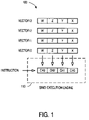
FIG. 1 illustrates one type of processing system 100 that includes a SIMD execution engine 110. In this case, the execution engine 110 receives an instruction (e.g., from an instruction memory unit) along with a four-component data vector (e.g., vector components X, Y, Z, and W, each having bits, laid out for processing on corresponding channels 0 through 3 of the SIMD execution engine 110). The engine 110 may then simultaneously execute the instruction for all of the components in the vector. Such an approach is called a “horizontal,” “channel-parallel,” or “Array Of Structures (AOS)” implementation.
FIG. 2 illustrates another type of processing system 200 that includes a SIMD execution engine 210. In this case, the execution engine 210 receives an instruction along with four operands of data, where each operand is associated with a different vector (e.g., the four X components from vectors V0 through V3). Each vector may include, for example, three location values (e.g., X, Y, and Z) associated with a three-dimensional graphics location. The engine 210 may then simultaneously execute the instruction for all of the operands in a single instruction period. Such an approach is called a “vertical,” “channel-serial,” or “Structure Of Arrays (SOA)” implementation. Although some embodiments described herein are associated with a four and eight channel SIMD execution engines, note that a SIMD execution engine could have any number of channels more than one (e.g., embodiments might be associated with a thirty-two channel execution engine).
FIG. 3 illustrates a processing system 300 with an eight-channel SIMD execution engine 310. The execution engine 310 may include an eight-byte register file 320, such as an on-chip General Register File (GRF), that can be accessed using assembly language and/or machine code instructions. In particular, the register file 320 in FIG. 3 includes five registers (R0 through R4) and the execution engine 310 is executing the following hardware instruction:
add(8) R1 R3 R4

The “(8)” indicates that the instruction will be executed on operands for all eight execution channels. The “R1” is a destination operand (DEST), and “R3” and “R4” are source operands (SRC0 and SRC1, respectively). Thus, each of the eight single-byte data elements in R4 will be added to corresponding data elements in R3. The eight results are then stored in R1. In particular, the first byte of R4 will be added to the first byte of R3 and that result will be stored in the first byte of R1. Similarly, the second byte of R4 will be added to the second byte of R3 and that result will be stored in the second byte of R1, etc.
In some applications, it may be helpful to access information in a register file in various ways. For example, in a graphics application it might at some times be helpful to treat portions of the register file as a vector, a scalar, and/or an array of values. Such an approach may help reduce the amount of instruction and/or data moving, packing, unpacking, and/or shuffling and improve the performance of the system.
FIG. 4 is a flow chart of a method according to some embodiments. The flow charts described herein do not necessarily imply a fixed order to the actions, and embodiments may be performed in any order that is practicable. Note that any of the methods described herein may be performed by hardware, software (including microcode), firmware, or any combination of these approaches. For example, a hardware instruction mapping engine might be used to facilitate operation according to any of the embodiments described herein.
At 402, a region in a register file is described for an operand. The operand might be, for example, a destination or source operand of a machine code instruction to be executed by a SIMD execution engine. According to some embodiments, the described region is “dynamic” in that different regions in the register file may be defined at different times. The description of the region might be, for example, encoded in the machine code instruction. Note that more than one region in the register file might be described at one time.
At 404, it is arranged for information to be stored into (or retrieved from) the register file in accordance with the described region. For example, data from a first region might be compared to data in a second region, and a result might be stored in a third region on a per-channel basis.
FIG. 5 illustrates a processing system 500 with an eight-channel SIMD execution engine 510 according to some embodiments. In this example, three regions have been described for a register file 520 having five eight-byte registers (R0 through R4): a destination region (DEST) and two source regions (SRC0 and SRC1). The regions might have been defined, for example, by a machine code add instruction. Moreover, in this example all execution channels are being used and the data elements are assumed to be bytes of data (e.g., each of eight SRC1 bytes will be added to a corresponding SRC0 byte and the results will be stored in eight DEST bytes in the register file 520).
Each region description includes a register identifier and a “sub-register identifier” indicating a location of a first data element in the register file 520 (illustrated in FIG. 5 as an “origin” of RegNum.SubRegNum). The sub-register identifier might indicate, for example, an offset from the start of a register (e.g., and may be expressed using a physical number of bits or bytes or a number of data elements). For example, the DEST region in FIG. 5 has an origin of R0.2, indicating that first data element in the DEST region is located at byte two of the first register (R0). Similarly, the SRC0 region begins at byte three of R2 (R2.3) and the SCR1 region starts at the first byte of R4 (R4.0). Note that the described regions might not be aligned to the register file 520 (e.g., a region does not need to start at byte 0 and end at byte 7 of a single register).
Note that an origin might be defined in other ways. For example, the register file 520 may be considered as a contiguous 40-byte memory area. Moreover, a single 6-bit address origin could point to a byte within the register file 520. Note that a single 6-bit address origin is able to point to any byte within a register file of up to 64-byte memory area. As another example, the register file 520 might be considered as a contiguous 320-bit memory area. In this case, a single 9-bit address origin could point to a bit within the register file 520.
Each region description may further include a “width” of the region. The width might indicate, for example, a number of data elements associated with the described region within a register row. For example, the DEST region illustrated in FIG. 5 has a width of four data elements (e.g., four bytes). Since eight execution channels are being used (and, therefore eight one-byte results need to be stored), the “height” of the region is two data elements (e.g., the region will span two different registers). That is, the total number of data elements in the four-element wide, two-element high DEST region will be eight. The DEST region might be considered a two dimensional array of data elements including register rows and register columns.
Similarly, the SRC0 region is described as being four bytes wide (and therefore two rows or registers high) and the SRC1 region is described as being eight bytes wide (and therefore has a vertical height of one data element). Note that a single region may span different registers in the register file 520 (e.g., some of the DEST region illustrated in FIG. 5 is located in a portion of R0 and the rest is located in a portion of R1).
Although some embodiments discussed herein describe a width of a region, according to other embodiments a vertical height of the region is instead described (in which case the width of the region may be inferred based on the total number of data elements). Moreover, note that overlapping register regions may be defined in the register file 520 (e.g., the region defined by SRC0 might partially or completely overlap the region defined by SRC1). In addition, although some examples discussed herein have two source operands and one destination operand, other types of instructions may be used. For example, an instruction might have one source operand and one destination operand, three source operands and two destination operands, etc.
According to some embodiment, a described region origin and width might result in a region “wrapping” to the next register in the register file 520. For example, a region of byte-size data elements having an origin of R2.6 and a width of eight would include the last bytes of R2 along with the first six bytes of R3. Similarly, a region might wrap from the bottom of the register file 520 to the top (e.g., from R4 to R0).
The SIMD execution engine 510 may add each byte in the described SRC1 region to a corresponding byte in the described SRC0 region and store the results the described DEST region in the register file 520. For example, FIG 6 illustrates execution channel mapping in the register file 620 according to some embodiments. In this case, data elements are arranged within a described region in a row-major order. Consider, for example, channel 6 of the execution engine 510. This channel will add the value stored in byte six of R4 to the value stored in byte five of R3 and store the result in byte four of R1. According to other embodiments, data elements may arranged within a described region in a column-major order or using any other mapping technique.
FIG. 7 illustrates a region description including a “horizontal stride” according to some embodiments. The horizontal stride may, for example, indicate a column offset between columns of data elements in a register file 720. In particular, the region described in FIG. 7 is for eight single-byte data elements (e.g., the region might be appropriate when only eight channels of a sixteen-channel SIMD execution engine are being used by a machine code instruction). The region is four bytes wide, and therefore two data elements high (such that the region will include eight data elements) and beings at R1.1 (byte 1 of R1).
In this case, a horizontal stride of two has been described. As a result, each data element in a row is offset from its neighboring data element in that row by two bytes. For example, the data element associated with channel 5 of the execution engine is located at byte 3 of R2 and the data element associated with channel 6 is located at byte 5 of R2. In this way, a described region may not be contiguous in the register file 720. Note that when a horizontal stride of one is described, the result would be a contiguous 4×2 array of bytes beginning at R1.1 in the two dimensional map of the register file 720.
The region described in FIG. 7 might be associated with a source operand, in which case data may be gathered from the non-contiguous areas when an instruction is executed. The region described in FIG. 7 might also be associated with a destination operand, in which case results may be scattered to the non-contiguous areas when an instruction is executed.
FIG. 8 illustrates a region description including a horizontal stride of “zero” according to some embodiments. As with FIG. 7, the region is for eight single-byte data elements and is four bytes wide (and therefore two data elements high). Because the horizontal stride is zero, however, each of the four elements in the first row map to the same physical location in the register file 820 (e.g., they are offset from their neighboring data element by zero). As a result, the value in R1.1 is replicated for the first four execution channels. When the region is associated with a source operand of an “add” instruction, for example, that same value would be used by all the first four execution channels. Similarly, the value in R2.1 is replicated for the last four execution channels.
According to some embodiments, the value of a horizontal stride may be encoded in an instruction. For example, a 3-bit field might be used to describe the following eight potential horizontal stride values: 0, 1, 2, 4, 8, 16, 32, and 64. Moreover, a negative horizontal stride may be described according to some embodiments.
Note that a region may be described for data elements of various sizes. For example, FIG. 9 illustrates a region description for word type data elements according to some embodiments. In this case, the register file 920 has eight sixteen-byte registers (R0 through R7, each having 128 bits), and the region begins at R2.3. The execution size is eight channels, and the width of the region is four data elements. Moreover, each data element is described as being one word (two bytes), and therefore the data element associated with the first execution channel (CH0) occupies both byte 3 and 4 of R2. Note that the horizontal stride of this region is one. In addition to byte and word type data elements, embodiments may be associated with other types of data elements (e.g., bit or float type elements).
FIG. 10 illustrates a region description including a “vertical stride” according to some embodiments. The vertical stride might, for example, indicate a row offset between rows of data elements in a register file 1020. As in FIG. 9, the register file 1020 has eight sixteen-byte registers (R0 through R7), and the region begins at R2.3. The execution size is eight channels, and the width of the region is four single word data elements (implying a row height of two for the region). In this case, however, a vertical stride of two has been described. As a result, each data element in a column is offset from its neighboring data element in that column by two registers. For example, the data element associated with channel 3 of the execution engine is located at bytes 9 and 10 of R2 and the data element associated with channel 7 is located at bytes 9 and 10 of R4. As with the horizontal stride, the described region is not contiguous in the register file 1020. Note that when a vertical stride of one is described, the result would be a contiguous 4×2 array of words beginning at R2.3 in the two dimensional map of the register file 1020.
The region described in FIG. 10 might be associated with a source operand, in which case data may be gathered from the non-contiguous areas when an instruction is executed. The region described in FIG. 10 might also be associated with a destination operand, in which case results may be scattered to the non-contiguous areas when an instruction is executed. According to some embodiments, a vertical stride might be described as data element column offset betweens rows of data elements (e.g., as described with respect to FIG. 14). Also note that a vertical stride might be less than, greater than, or equal to a horizontal stride.
FIG. 11 illustrates a region description including a vertical stride of “zero” according to some embodiments. As with FIGS. 9 and 10, the region is for eight single-word data elements and is four words wide (and therefore two data elements high). Because the vertical stride is zero, however, both of the elements in the first column map to the same location in the register file 1120 (e.g., they are offset from each other by zero). As a result, the word at bytes 3-4 of R2 is replicated for those two execution channels (e.g., channels 0 and 4). When the region is associated with a source operand of a “compare” instruction, for example, that same value would be used by both execution channels. Similarly, the word at bytes 5-6 of R2 is replicated for the channels 1 and 5 of the SIMD execution engine, etc. In addition, the value of a vertical stride may be encoded in an instruction, and, according to some embodiments, a negative vertical stride may be described.
According to some embodiments, a vertical stride might be defined as a number of data elements in a register file 1220 (instead of a number of register rows). For example, FIG. 12 illustrates a region description having a 1-data element (1-word) vertical stride according to some embodiments. Thus, the first “row” of the array defined by the region comprises four words from R2.3 through R2.10. The second row is offset by a single word and spans from R2.5 through R2.12. Such an implementation might be associated with, for example, a sliding window for a filtering operation.
FIG. 13 illustrates a region description wherein both the horizontal and vertical strides are zero according to some embodiments. As a result, all eight execution channels are mapped to a single location in the register file 1320 (e.g., bytes 3-4 of R2). When the region is associated with a machine code instruction, therefore, the single value at bytes 3-4 of R2 may be used by all eight of the execution channels.
Note that different types of descriptions may be provided for different instructions. For example, a first instruction might define a destination region as a 4×4 array while the next instruction defines a region as a 1×16 array. Moreover, different types of regions may be described for a single instruction.
Consider, for example, the register file 1420 illustrated in FIG. 14 having eight thirty-two-byte registers (R0 through R7, each having 256 bits). Note that in this illustration, each register is shown as being two “rows” and sample values are shown in each location of a region.
In this example, regions are described for an operand within an instruction as follows:
RegFile RegNum.SubRegNum<VertStride; Width,HorzStride>:type
where RegFile identifies the name space for the register file 1420, RegNum points a register in the register file 1420 (e.g., R0 through R7), SubRegNum is a byte-offset from the beginning of that register, VertStride describes a vertical stride, Width describes the width of the region, HorzStride describes a horizontal stride, and type indicates the size of each data element (e.g., “b” for byte-size and “w” for word-size data elements). According to some embodiments, SubRegNum may be described as a number of data elements (instead of a number of bytes). Similarly, VertStride, Width, and HorzStride could be described as a number of bytes (instead of a number of data elements).
FIG. 14 illustrates a machine code add instruction being executed by eight channels of a SIMD execution engine. In particular, each of the eight bytes described by R2.17<16;2,1>b (SRC1) are added to each of the eight bytes described by R1.14<16;4,0>:b (SRC0). The eight results are stored in each of the eight words described by R5.3<18;4,3>:w (DEST).
SRC1 is two bytes wide, and therefore four data elements high, and begins in byte 17 of R2 (illustrated in FIG. 14 as the second byte of the second row of R2). The horizontal stride is one. In this case, the vertical stride is described as a number of data element columns separating one row of the region from a neighboring row (as opposed to a row offset between rows as discussed with respect to FIG. 10). That is, the start of one row is offset from the start of the next row of the region by 16 bytes. In particular, the first row starts at R2.17 and the second row of the region starts at R3.1 (counting from right-to-left starting at R2.17 and wrapping to the next register when the end of R2 is reached). Similarly, the third row starts at R3.17.
SRC0 is four bytes wide, and therefore two data elements high, and begins at R1.14. Because the horizontal stride is zero, the value at location R1.14 (e.g., “2” as illustrated in FIG. 14) maps to the first four execution channels and value at location R1.30 (based on the vertical stride of 16) maps to the next four execution channels.
DEST is four words wide, and therefore two data elements high, and begins at R5.3. Thus, the execution channel will add the value “1” (the first data element of the SRC0 region) to the value “2” (the data element of the SRC1 region that will be used by the first four execution channels) and the result “3” is stored into bytes 3 and 4 of R5 (the first word-size data element of the DEST region).
The horizontal stride of DEST is three data elements, so the next data element is the word beginning at byte 9 of R5 (e.g., offset from byte 3 by three words), the element after that begins at bye 15 of R5 (shown broken across two rows in FIG. 14), and the last element in the first row of the DEST region starts at byte 21 of R5.
The vertical stride of DEST is eighteen data elements, so the first data element of the second “row” of the DEST array begins at byte 7 of R6. The result stored in this DEST location is “6” representing the “3” from the fifth data element of SRC0 region added to the “3” from the SRC1 region which applies to execution channels 4 through 7.
Because information in the register files may be efficiently and flexibly accessed in different ways, the performance of a system may be improved. For example, machine code instructions may efficiently be used in connection with a replicated scalar, a vector of a replicated scalar, a replicated vector, a two-dimensional array, a sliding window, and/or a related list of one-dimensional arrays. As a result, the amount of data moves, packing, unpacking, and or shuffling instructions may be reduced—which can improve the performance of an application or algorithm, such as one associated with a media kernel.
Note that in some cases, restrictions might be placed on region descriptions. For example, a sub-register origin and/or a vertical stride might be permitted for source operands but not destination operands. Moreover, physical characteristics of a register file might limit region descriptions. For example, a relatively large register file might be implemented using embedded Random Access Memory (RAM), and the cost and power associated with the embedded RAM might depended on the number of read and write ports that are provided. Thus, the number of read and write points (and the arrangement of the registers in the RAM) might restrict region descriptions.
FIG. 15 is a block diagram of a system 1500 according to some embodiments. The system 1500 might be associated with, for example, a media processor adapted to record and/or display digital television signals. The system 1500 includes a processor 1510 that has an n-operand SIMD execution engine 1520 in accordance with any of the embodiments described herein. For example, the SIMD execution engine 1520 might include a register file and an instruction mapping engine to map operands to a dynamic region of the register file defined by an instruction. The processor 1510 may be associated with, for example, a general purpose processor, a digital signal processor, a media processor, a graphics processor, or a communication processor.
The system 1500 may also include an instruction memory unit 1530 to store SIMD instructions and a data memory unit 1540 to store data (e.g., scalars and vectors associated with a two-dimensional image, a three-dimensional image, and/or a moving image). The instruction memory unit 1530 and the data memory unit 1540 may comprise, for example, RAM units. Note that the instruction memory unit 1530 and/or the data memory unit 1540 might be associated with separate instruction and data caches, a shared instruction and data cache, separate instruction and data caches backed by a common shared cache, or any other cache hierarchy. According to some embodiments, the system 1500 also includes a hard disk drive (e.g., to store and provide media information) and/or a non-volatile memory such as FLASH memory (e.g., to store and provide instructions and data).
The following illustrates various additional embodiments. These do not constitute a definition of all possible embodiments, and those skilled in the art will understand that many other embodiments are possible. Further, although the following embodiments are briefly described for clarity, those skilled in the art will understand how to make any changes, if necessary, to the above description to accommodate these and other embodiments and applications.
Although various ways of describing source and/or destination operands have been discussed, note that embodiments may be use any subset or combination of such descriptions. For example, a source operand might be permitted to have a vertical stride while a vertical stride might not be permitted for a destination operand.
Note that embodiments may be implemented in any of a number of different ways. For example, the following code might compute the addresses of data elements assigned to execution channels when the destination register is aligned to a 256-bit register boundary:
// Input: Type: b | ub | w | uw | d | ud | f
// RegNum: In unit of 256-bit register
// SubRegNum: In unit of data element size
// ExecSize, Width, VertStride, HorzStride:
   In unit of data elements
// Output: Address[0:ExecSize−1] for execution channels
int ElementSize = (Type==“b”||Type==“ub”) ? 1 :
(Type==“w”|Type==“uw”) ? 2 : 4;
int Height = ExecSize / Width;
int Channel = 0;
int RowBase = RegNum<<5 + SubRegNum * ElementSize;
for (int y=0; y<Height; y++) {
int Offset = RowBase;
for (int x=0; x<Width; x++) {
Address [Channel++] = Offset;
Offset += HorzStride*ElementSize;
}
RowBase += VertStride * ElementSize;
}
According to some embodiments, a register region is encoded in an instruction word for each of the instruction's operands. For example, the register number and sub-register number of the origin may be encoded. In some cases, the value in the instruction word may represent a different value in terms of the actual description. For example, three bits might be used to encode the width of a region, and “011” might represent a width of eight elements while “100” represents a width of sixteen elements. In this way, a larger range of descriptions may be available as compared to simply encoding the actual value of the description in the instruction word.
Moreover, some embodiments have been described herein with respect to a SIMD execution engine. Note, however, that embodiments may be associated with other types of execution engines, such as a Multiple Instruction, Multiple Data (MIMD) execution engine.
The several embodiments described herein are solely for the purpose of illustration. Persons skilled in the art will recognize from this description other embodiments may be practiced with modifications and alterations limited only by the claims.

Claims (24)

1. A method, comprising:
defining, for an operand, an origin comprising a register identifier and a sub-register identifier of a dynamic region in a register file comprising a plurality of bytes, wherein the dynamic region is to store multiple data elements, each data element being associated with an execution channel of an execution engine; and
storing information into or retrieving information from the register file in accordance with the dynamic region, wherein the sub-register identifier indicates an offset from a start of a register and wherein the offset is to point to any of the plurality of bytes.
2. The method of claim 1, wherein the defined origin and the offset are included in a single instruction, multiple data machine code instruction.
3. The method of claim 1, wherein the operand is one of a source operand or a destination operand.
4. The method of claim 1, further comprising:
defining multiple dynamic regions for multiple operands.
5. The method of claim 1, wherein the defined dynamic region spans different registers in the register file.
6. The method of claim 1, wherein the defined dynamic region is not contiguous in the register file.
7. The method of claim 1, wherein the defined dynamic region is not aligned to registers in the register file.
8. The method of claim 1, wherein the register file includes register rows and register columns.
9. The method of claim 8, wherein data elements are arranged within the defined region in one of: (i) row-major order, or (ii) column-major order.
10. The method of claim 8, wherein said defining includes a width indicating a number of data elements associated with the defined region within a register row.
11. The method of claim 8, wherein said defining includes a horizontal stride indicating an offset between columns of data elements in the register file.
12. The method of claim 8, wherein said defining includes a vertical stride indicating at least one of: (i) a row offset between rows of data elements in the register file or (ii) a data element offset between rows of data elements in the register file.
13. The method of claim 1, wherein said defining includes a data type indicating a size of each data element.
14. The method of claim 1, wherein said defining includes an execution size indicating a number of data elements associated with the defined region.
15. The method of claim 1, wherein the defined region is associated with at least one of: (i) replicated scalar, (ii) a vector of a replicated scalar, (iii) a replicated vector, (iv) a two-dimensional array, (v) a sliding window, or (vi) a related list of one-dimensional arrays.
16. An apparatus, comprising:
a single instruction, multiple data execution engine;
a register file on the same die as the execution engine; and
an instruction mapping engine to define, for an operand, an origin comprising a register identifier and a sub-register identifier of a dynamic region in a register file comprising a plurality of bytes, wherein the dynamic region is to store multiple data elements, each data element being associated with an execution channel of an execution engine, and is to store information into or is to retrieve information from the register file in accordance with the dynamic region, wherein the sub-register identifier indicates an offset from a start of a register and wherein the offset is to point to any of the plurality of bytes.
17. The apparatus of claim 16, wherein the defined region spans different registers in the register file.
18. The apparatus of claim 16, wherein the defined region is not contiguous in the register file.
19. The apparatus of claim 16, wherein the register file includes register rows and register columns, and the instruction mapping engine defines the portion based on a description including, (i) a width, and (ii) a horizontal stride.
20. A system, comprising:
an n-channel single instruction, multiple-data execution engine, n being an integer greater than 1;
a register file; and
an instruction mapping engine to define, for an operand, an origin comprising a register identifier and a sub-register identifier of a dynamic region in a register file comprising a plurality of bytes, wherein the dynamic region is to store multiple data elements, each data element being associated with an execution channel of an execution engine, and is to store information into or is to retrieve information from the register file in accordance with the dynamic region, wherein the sub-register identifier indicates an offset from a start of a register and wherein the offset is to point to any of the plurality of bytes; and
a graphics data memory unit.
21. The system of claim 19, wherein the instruction mapping engine scatters data to areas of the register file.
22. The system of claim 21, wherein the areas are non-contiguous in the register file.
23. The system of claim 19, wherein the instruction mapping engine gathers data from areas of the register file.
24. The system of claim 23, wherein the areas are non-contiguous in the register file.
US11/024,298 2004-12-28 2004-12-28 Register file regions for a processing system Expired - Fee Related US7257695B2 (en)

Priority Applications (8)

Application Number Priority Date Filing Date Title
US11/024,298 US7257695B2 (en) 2004-12-28 2004-12-28 Register file regions for a processing system
TW094146729A TWI300187B (en) 2004-12-28 2005-12-27 Method, apparatus and system to enable register information to be flexibly accessed for an execution engine
CNB2005101217007A CN100492280C (en) 2004-12-28 2005-12-28 Method, device and system for accessing information in file region of register
DE112005003265T DE112005003265T5 (en) 2004-12-28 2005-12-28 Register file spaces for a processing system
PCT/US2005/047279 WO2006071947A1 (en) 2004-12-28 2005-12-28 Register file regions for a processing system
KR1020077014692A KR100935308B1 (en) 2004-12-28 2005-12-28 Register file regions for a processing system
GB0714452A GB2436506B (en) 2004-12-28 2007-07-24 Register file regions for a processing system
US11/829,249 US20080022069A1 (en) 2004-12-28 2007-07-27 Register file regions for a processing system

Applications Claiming Priority (1)

Application Number Priority Date Filing Date Title
US11/024,298 US7257695B2 (en) 2004-12-28 2004-12-28 Register file regions for a processing system

Related Child Applications (1)

Application Number Title Priority Date Filing Date
US11/829,249 Continuation US20080022069A1 (en) 2004-12-28 2007-07-27 Register file regions for a processing system

Publications (2)

Publication Number Publication Date
US20060149937A1 US20060149937A1 (en) 2006-07-06
US7257695B2 true US7257695B2 (en) 2007-08-14

Family

ID=36498848

Family Applications (2)

Application Number Title Priority Date Filing Date
US11/024,298 Expired - Fee Related US7257695B2 (en) 2004-12-28 2004-12-28 Register file regions for a processing system
US11/829,249 Abandoned US20080022069A1 (en) 2004-12-28 2007-07-27 Register file regions for a processing system

Family Applications After (1)

Application Number Title Priority Date Filing Date
US11/829,249 Abandoned US20080022069A1 (en) 2004-12-28 2007-07-27 Register file regions for a processing system

Country Status (7)

Country Link
US (2) US7257695B2 (en)
KR (1) KR100935308B1 (en)
CN (1) CN100492280C (en)
DE (1) DE112005003265T5 (en)
GB (1) GB2436506B (en)
TW (1) TWI300187B (en)
WO (1) WO2006071947A1 (en)

Cited By (29)

* Cited by examiner, † Cited by third party
Publication number Priority date Publication date Assignee Title
US20080082797A1 (en) * 2006-10-03 2008-04-03 Hong Kong Applied Science and Technology Research Institute Company Limited Configurable Single Instruction Multiple Data Unit
US20090198966A1 (en) * 2008-01-31 2009-08-06 Gschwind Michael K Multi-Addressable Register File
US20090198977A1 (en) * 2008-01-31 2009-08-06 Gschwind Michael K Sharing Data in Internal and Memory Representations with Dynamic Data-Driven Conversion
US20130091340A1 (en) * 2006-04-12 2013-04-11 Soft Machines, Inc. Apparatus and Method for Processing an Instruction Matrix Specifying Parallel and Dependent Operations
US9395981B2 (en) 2011-09-16 2016-07-19 International Business Machines Corporation Multi-addressable register files and format conversions associated therewith
US9632801B2 (en) 2014-04-09 2017-04-25 Intel Corporation Banked memory access efficiency by a graphics processor
US9727336B2 (en) 2011-09-16 2017-08-08 International Business Machines Corporation Fine-grained instruction enablement at sub-function granularity based on an indicated subrange of registers
US9766893B2 (en) 2011-03-25 2017-09-19 Intel Corporation Executing instruction sequence code blocks by using virtual cores instantiated by partitionable engines
US9811342B2 (en) 2013-03-15 2017-11-07 Intel Corporation Method for performing dual dispatch of blocks and half blocks
US9811377B2 (en) 2013-03-15 2017-11-07 Intel Corporation Method for executing multithreaded instructions grouped into blocks
US9823930B2 (en) 2013-03-15 2017-11-21 Intel Corporation Method for emulating a guest centralized flag architecture by using a native distributed flag architecture
US9842005B2 (en) 2011-03-25 2017-12-12 Intel Corporation Register file segments for supporting code block execution by using virtual cores instantiated by partitionable engines
US9858080B2 (en) 2013-03-15 2018-01-02 Intel Corporation Method for implementing a reduced size register view data structure in a microprocessor
US9886279B2 (en) 2013-03-15 2018-02-06 Intel Corporation Method for populating and instruction view data structure by using register template snapshots
US9891924B2 (en) 2013-03-15 2018-02-13 Intel Corporation Method for implementing a reduced size register view data structure in a microprocessor
US9898412B2 (en) 2013-03-15 2018-02-20 Intel Corporation Methods, systems and apparatus for predicting the way of a set associative cache
US9921845B2 (en) 2011-03-25 2018-03-20 Intel Corporation Memory fragments for supporting code block execution by using virtual cores instantiated by partitionable engines
US9934042B2 (en) 2013-03-15 2018-04-03 Intel Corporation Method for dependency broadcasting through a block organized source view data structure
US9940134B2 (en) 2011-05-20 2018-04-10 Intel Corporation Decentralized allocation of resources and interconnect structures to support the execution of instruction sequences by a plurality of engines
US9965281B2 (en) 2006-11-14 2018-05-08 Intel Corporation Cache storing data fetched by address calculating load instruction with label used as associated name for consuming instruction to refer
US10031784B2 (en) 2011-05-20 2018-07-24 Intel Corporation Interconnect system to support the execution of instruction sequences by a plurality of partitionable engines
US10140138B2 (en) 2013-03-15 2018-11-27 Intel Corporation Methods, systems and apparatus for supporting wide and efficient front-end operation with guest-architecture emulation
US10146548B2 (en) 2013-03-15 2018-12-04 Intel Corporation Method for populating a source view data structure by using register template snapshots
US10169045B2 (en) 2013-03-15 2019-01-01 Intel Corporation Method for dependency broadcasting through a source organized source view data structure
US10191746B2 (en) 2011-11-22 2019-01-29 Intel Corporation Accelerated code optimizer for a multiengine microprocessor
US10198266B2 (en) 2013-03-15 2019-02-05 Intel Corporation Method for populating register view data structure by using register template snapshots
US10228949B2 (en) 2010-09-17 2019-03-12 Intel Corporation Single cycle multi-branch prediction including shadow cache for early far branch prediction
US10521239B2 (en) 2011-11-22 2019-12-31 Intel Corporation Microprocessor accelerated code optimizer
US11188332B2 (en) 2019-05-10 2021-11-30 International Business Machines Corporation System and handling of register data in processors

Families Citing this family (9)

* Cited by examiner, † Cited by third party
Publication number Priority date Publication date Assignee Title
US20080162522A1 (en) * 2006-12-29 2008-07-03 Guei-Yuan Lueh Methods and apparatuses for compaction and/or decompaction
US8453127B2 (en) 2010-09-20 2013-05-28 Sap Ag Systems and methods providing a token synchronization gateway for a graph-based business process model
US9552206B2 (en) * 2010-11-18 2017-01-24 Texas Instruments Incorporated Integrated circuit with control node circuitry and processing circuitry
US10255228B2 (en) * 2011-12-06 2019-04-09 Nvidia Corporation System and method for performing shaped memory access operations
CN104025021A (en) * 2011-12-23 2014-09-03 英特尔公司 Apparatus and method for sliding window data gather
US10001995B2 (en) * 2015-06-02 2018-06-19 Intel Corporation Packed data alignment plus compute instructions, processors, methods, and systems
CN104898991B (en) * 2015-06-10 2018-07-27 烽火通信科技股份有限公司 A kind of register access methods and system based on automation RAL
US20170177350A1 (en) * 2015-12-18 2017-06-22 Intel Corporation Instructions and Logic for Set-Multiple-Vector-Elements Operations
US10289416B2 (en) 2015-12-30 2019-05-14 Intel Corporation Systems, apparatuses, and methods for lane-based strided gather

Citations (6)

* Cited by examiner, † Cited by third party
Publication number Priority date Publication date Assignee Title
US5513366A (en) * 1994-09-28 1996-04-30 International Business Machines Corporation Method and system for dynamically reconfiguring a register file in a vector processor
US5812147A (en) * 1996-09-20 1998-09-22 Silicon Graphics, Inc. Instruction methods for performing data formatting while moving data between memory and a vector register file
US6175892B1 (en) 1998-06-19 2001-01-16 Hitachi America. Ltd. Registers and methods for accessing registers for use in a single instruction multiple data system
US20020010847A1 (en) 1998-03-31 2002-01-24 Mohammad Abdallah Executing partial-width packed data instructions
US20020026570A1 (en) 2000-11-08 2002-02-28 Takehiro Shimizu SIMD operation system capable of designating plural registers
US20050108503A1 (en) * 2003-11-18 2005-05-19 International Business Machines Corporation Two dimensional addressing of a matrix-vector register array

Family Cites Families (1)

* Cited by examiner, † Cited by third party
Publication number Priority date Publication date Assignee Title
US7275148B2 (en) * 2003-09-08 2007-09-25 Freescale Semiconductor, Inc. Data processing system using multiple addressing modes for SIMD operations and method thereof

Patent Citations (6)

* Cited by examiner, † Cited by third party
Publication number Priority date Publication date Assignee Title
US5513366A (en) * 1994-09-28 1996-04-30 International Business Machines Corporation Method and system for dynamically reconfiguring a register file in a vector processor
US5812147A (en) * 1996-09-20 1998-09-22 Silicon Graphics, Inc. Instruction methods for performing data formatting while moving data between memory and a vector register file
US20020010847A1 (en) 1998-03-31 2002-01-24 Mohammad Abdallah Executing partial-width packed data instructions
US6175892B1 (en) 1998-06-19 2001-01-16 Hitachi America. Ltd. Registers and methods for accessing registers for use in a single instruction multiple data system
US20020026570A1 (en) 2000-11-08 2002-02-28 Takehiro Shimizu SIMD operation system capable of designating plural registers
US20050108503A1 (en) * 2003-11-18 2005-05-19 International Business Machines Corporation Two dimensional addressing of a matrix-vector register array

Non-Patent Citations (1)

* Cited by examiner, † Cited by third party
Title
"PCT International Search Report of the International Searching Authority", mailed Jun. 20, 2006, for PCT/US2005/047279, 4pgs.

Cited By (52)

* Cited by examiner, † Cited by third party
Publication number Priority date Publication date Assignee Title
US20130091340A1 (en) * 2006-04-12 2013-04-11 Soft Machines, Inc. Apparatus and Method for Processing an Instruction Matrix Specifying Parallel and Dependent Operations
US9886416B2 (en) 2006-04-12 2018-02-06 Intel Corporation Apparatus and method for processing an instruction matrix specifying parallel and dependent operations
US10289605B2 (en) 2006-04-12 2019-05-14 Intel Corporation Apparatus and method for processing an instruction matrix specifying parallel and dependent operations
US11163720B2 (en) 2006-04-12 2021-11-02 Intel Corporation Apparatus and method for processing an instruction matrix specifying parallel and dependent operations
US9053292B2 (en) * 2006-04-12 2015-06-09 Soft Machines, Inc. Processor executing super instruction matrix with register file configurable for single or multiple threads operations
US20080082797A1 (en) * 2006-10-03 2008-04-03 Hong Kong Applied Science and Technology Research Institute Company Limited Configurable Single Instruction Multiple Data Unit
US7441099B2 (en) * 2006-10-03 2008-10-21 Hong Kong Applied Science and Technology Research Institute Company Limited Configurable SIMD processor instruction specifying index to LUT storing information for different operation and memory location for each processing unit
US10585670B2 (en) 2006-11-14 2020-03-10 Intel Corporation Cache storing data fetched by address calculating load instruction with label used as associated name for consuming instruction to refer
US9965281B2 (en) 2006-11-14 2018-05-08 Intel Corporation Cache storing data fetched by address calculating load instruction with label used as associated name for consuming instruction to refer
US20090198966A1 (en) * 2008-01-31 2009-08-06 Gschwind Michael K Multi-Addressable Register File
US20090198977A1 (en) * 2008-01-31 2009-08-06 Gschwind Michael K Sharing Data in Internal and Memory Representations with Dynamic Data-Driven Conversion
US7877582B2 (en) 2008-01-31 2011-01-25 International Business Machines Corporation Multi-addressable register file
US7849294B2 (en) 2008-01-31 2010-12-07 International Business Machines Corporation Sharing data in internal and memory representations with dynamic data-driven conversion
US10228949B2 (en) 2010-09-17 2019-03-12 Intel Corporation Single cycle multi-branch prediction including shadow cache for early far branch prediction
US10564975B2 (en) 2011-03-25 2020-02-18 Intel Corporation Memory fragments for supporting code block execution by using virtual cores instantiated by partitionable engines
US9921845B2 (en) 2011-03-25 2018-03-20 Intel Corporation Memory fragments for supporting code block execution by using virtual cores instantiated by partitionable engines
US9766893B2 (en) 2011-03-25 2017-09-19 Intel Corporation Executing instruction sequence code blocks by using virtual cores instantiated by partitionable engines
US11204769B2 (en) 2011-03-25 2021-12-21 Intel Corporation Memory fragments for supporting code block execution by using virtual cores instantiated by partitionable engines
US9842005B2 (en) 2011-03-25 2017-12-12 Intel Corporation Register file segments for supporting code block execution by using virtual cores instantiated by partitionable engines
US9934072B2 (en) 2011-03-25 2018-04-03 Intel Corporation Register file segments for supporting code block execution by using virtual cores instantiated by partitionable engines
US9990200B2 (en) 2011-03-25 2018-06-05 Intel Corporation Executing instruction sequence code blocks by using virtual cores instantiated by partitionable engines
US10372454B2 (en) 2011-05-20 2019-08-06 Intel Corporation Allocation of a segmented interconnect to support the execution of instruction sequences by a plurality of engines
US9940134B2 (en) 2011-05-20 2018-04-10 Intel Corporation Decentralized allocation of resources and interconnect structures to support the execution of instruction sequences by a plurality of engines
US10031784B2 (en) 2011-05-20 2018-07-24 Intel Corporation Interconnect system to support the execution of instruction sequences by a plurality of partitionable engines
US9727337B2 (en) 2011-09-16 2017-08-08 International Business Machines Corporation Fine-grained instruction enablement at sub-function granularity based on an indicated subrange of registers
US9395981B2 (en) 2011-09-16 2016-07-19 International Business Machines Corporation Multi-addressable register files and format conversions associated therewith
US9411585B2 (en) 2011-09-16 2016-08-09 International Business Machines Corporation Multi-addressable register files and format conversions associated therewith
US9727336B2 (en) 2011-09-16 2017-08-08 International Business Machines Corporation Fine-grained instruction enablement at sub-function granularity based on an indicated subrange of registers
US10191746B2 (en) 2011-11-22 2019-01-29 Intel Corporation Accelerated code optimizer for a multiengine microprocessor
US10521239B2 (en) 2011-11-22 2019-12-31 Intel Corporation Microprocessor accelerated code optimizer
US9823930B2 (en) 2013-03-15 2017-11-21 Intel Corporation Method for emulating a guest centralized flag architecture by using a native distributed flag architecture
US9811377B2 (en) 2013-03-15 2017-11-07 Intel Corporation Method for executing multithreaded instructions grouped into blocks
US10146576B2 (en) 2013-03-15 2018-12-04 Intel Corporation Method for executing multithreaded instructions grouped into blocks
US10146548B2 (en) 2013-03-15 2018-12-04 Intel Corporation Method for populating a source view data structure by using register template snapshots
US10169045B2 (en) 2013-03-15 2019-01-01 Intel Corporation Method for dependency broadcasting through a source organized source view data structure
US9858080B2 (en) 2013-03-15 2018-01-02 Intel Corporation Method for implementing a reduced size register view data structure in a microprocessor
US10198266B2 (en) 2013-03-15 2019-02-05 Intel Corporation Method for populating register view data structure by using register template snapshots
US9904625B2 (en) 2013-03-15 2018-02-27 Intel Corporation Methods, systems and apparatus for predicting the way of a set associative cache
US10248570B2 (en) 2013-03-15 2019-04-02 Intel Corporation Methods, systems and apparatus for predicting the way of a set associative cache
US10255076B2 (en) 2013-03-15 2019-04-09 Intel Corporation Method for performing dual dispatch of blocks and half blocks
US10275255B2 (en) 2013-03-15 2019-04-30 Intel Corporation Method for dependency broadcasting through a source organized source view data structure
US10140138B2 (en) 2013-03-15 2018-11-27 Intel Corporation Methods, systems and apparatus for supporting wide and efficient front-end operation with guest-architecture emulation
US9811342B2 (en) 2013-03-15 2017-11-07 Intel Corporation Method for performing dual dispatch of blocks and half blocks
US10503514B2 (en) 2013-03-15 2019-12-10 Intel Corporation Method for implementing a reduced size register view data structure in a microprocessor
US9886279B2 (en) 2013-03-15 2018-02-06 Intel Corporation Method for populating and instruction view data structure by using register template snapshots
US9891924B2 (en) 2013-03-15 2018-02-13 Intel Corporation Method for implementing a reduced size register view data structure in a microprocessor
US11656875B2 (en) 2013-03-15 2023-05-23 Intel Corporation Method and system for instruction block to execution unit grouping
US10740126B2 (en) 2013-03-15 2020-08-11 Intel Corporation Methods, systems and apparatus for supporting wide and efficient front-end operation with guest-architecture emulation
US9898412B2 (en) 2013-03-15 2018-02-20 Intel Corporation Methods, systems and apparatus for predicting the way of a set associative cache
US9934042B2 (en) 2013-03-15 2018-04-03 Intel Corporation Method for dependency broadcasting through a block organized source view data structure
US9632801B2 (en) 2014-04-09 2017-04-25 Intel Corporation Banked memory access efficiency by a graphics processor
US11188332B2 (en) 2019-05-10 2021-11-30 International Business Machines Corporation System and handling of register data in processors

Also Published As

Publication number Publication date
TW200634622A (en) 2006-10-01
WO2006071947A1 (en) 2006-07-06
KR20070097049A (en) 2007-10-02
CN1821952A (en) 2006-08-23
US20060149937A1 (en) 2006-07-06
US20080022069A1 (en) 2008-01-24
GB0714452D0 (en) 2007-09-05
TWI300187B (en) 2008-08-21
GB2436506A (en) 2007-09-26
DE112005003265T5 (en) 2007-11-15
GB2436506B (en) 2009-01-28
KR100935308B1 (en) 2010-01-06
CN100492280C (en) 2009-05-27

Similar Documents

Publication Publication Date Title
US7257695B2 (en) Register file regions for a processing system
US20060149938A1 (en) Determining a register file region based at least in part on a value in an index register
US20240012644A1 (en) Efficient direct convolution using simd instructions
US20070011442A1 (en) Systems and methods of providing indexed load and store operations in a dual-mode computer processing environment
JP7101776B2 (en) Systems and methods for converting matrix inputs to vectorized inputs for matrix processors
KR100904318B1 (en) Conditional instruction for a single instruction, multiple data execution engine
US6665790B1 (en) Vector register file with arbitrary vector addressing
JP5461533B2 (en) Local and global data sharing
RU2006124547A (en) REPLACING DATA PROCESSING REGISTERS
CN108205448B (en) Stream engine with multi-dimensional circular addressing selectable in each dimension
JP2002518730A (en) Register and method for accessing register used in single instruction multiple data system
US20060092161A1 (en) Method and apparatus for management of bit plane resources
JP4901754B2 (en) Evaluation unit for flag register of single instruction multiple data execution engine
US20080162522A1 (en) Methods and apparatuses for compaction and/or decompaction
US7441099B2 (en) Configurable SIMD processor instruction specifying index to LUT storing information for different operation and memory location for each processing unit
WO2022068328A1 (en) Data migration method and apparatus, and processor and calculation device
US20220188380A1 (en) Data processing method and apparatus applied to graphics processing unit, and electronic device
US20080162879A1 (en) Methods and apparatuses for aligning and/or executing instructions
US20120260062A1 (en) System and method for providing dynamic addressability of data elements in a register file with subword parallelism
JP3706633B2 (en) Processor with instruction cache
WO2022067510A1 (en) Processor, processing method, and related device
CN114298890A (en) Data processing apparatus and method thereof
GB2617828A (en) Technique for handling data elements stored in an array storage

Legal Events

Date Code Title Description
AS Assignment

Owner name: INTEL CORPORATION, CALIFORNIA

Free format text: ASSIGNMENT OF ASSIGNORS INTEREST;ASSIGNORS:JIANG, HONG;COOK, VAL;REEL/FRAME:015900/0983;SIGNING DATES FROM 20050411 TO 20050413

STCF Information on status: patent grant

Free format text: PATENTED CASE

FPAY Fee payment

Year of fee payment: 4

FPAY Fee payment

Year of fee payment: 8

FEPP Fee payment procedure

Free format text: MAINTENANCE FEE REMINDER MAILED (ORIGINAL EVENT CODE: REM.); ENTITY STATUS OF PATENT OWNER: LARGE ENTITY

LAPS Lapse for failure to pay maintenance fees

Free format text: PATENT EXPIRED FOR FAILURE TO PAY MAINTENANCE FEES (ORIGINAL EVENT CODE: EXP.); ENTITY STATUS OF PATENT OWNER: LARGE ENTITY

STCH Information on status: patent discontinuation

Free format text: PATENT EXPIRED DUE TO NONPAYMENT OF MAINTENANCE FEES UNDER 37 CFR 1.362

FP Lapsed due to failure to pay maintenance fee

Effective date: 20190814