US7315916B2 - Scratch pad block - Google Patents
Scratch pad block Download PDFInfo
- Publication number
- US7315916B2 US7315916B2 US11/016,285 US1628504A US7315916B2 US 7315916 B2 US7315916 B2 US 7315916B2 US 1628504 A US1628504 A US 1628504A US 7315916 B2 US7315916 B2 US 7315916B2
- Authority
- US
- United States
- Prior art keywords
- data
- block
- sector
- page
- sectors
- Prior art date
- Legal status (The legal status is an assumption and is not a legal conclusion. Google has not performed a legal analysis and makes no representation as to the accuracy of the status listed.)
- Active, expires
Links
Images
Classifications
-
- G—PHYSICS
- G06—COMPUTING; CALCULATING OR COUNTING
- G06F—ELECTRIC DIGITAL DATA PROCESSING
- G06F12/00—Accessing, addressing or allocating within memory systems or architectures
- G06F12/02—Addressing or allocation; Relocation
- G06F12/0223—User address space allocation, e.g. contiguous or non contiguous base addressing
- G06F12/023—Free address space management
- G06F12/0238—Memory management in non-volatile memory, e.g. resistive RAM or ferroelectric memory
- G06F12/0246—Memory management in non-volatile memory, e.g. resistive RAM or ferroelectric memory in block erasable memory, e.g. flash memory
-
- G—PHYSICS
- G11—INFORMATION STORAGE
- G11C—STATIC STORES
- G11C16/00—Erasable programmable read-only memories
- G11C16/02—Erasable programmable read-only memories electrically programmable
- G11C16/06—Auxiliary circuits, e.g. for writing into memory
- G11C16/10—Programming or data input circuits
-
- G—PHYSICS
- G11—INFORMATION STORAGE
- G11C—STATIC STORES
- G11C16/00—Erasable programmable read-only memories
- G11C16/02—Erasable programmable read-only memories electrically programmable
- G11C16/06—Auxiliary circuits, e.g. for writing into memory
- G11C16/34—Determination of programming status, e.g. threshold voltage, overprogramming or underprogramming, retention
-
- G—PHYSICS
- G06—COMPUTING; CALCULATING OR COUNTING
- G06F—ELECTRIC DIGITAL DATA PROCESSING
- G06F2212/00—Indexing scheme relating to accessing, addressing or allocation within memory systems or architectures
- G06F2212/72—Details relating to flash memory management
- G06F2212/7203—Temporary buffering, e.g. using volatile buffer or dedicated buffer blocks
Definitions
- This invention relates generally to the operation of non-volatile flash memory systems, and, more specifically, to more efficient methods of programming data within a non-volatile flash memory.
- non-volatile memory products are used today, particularly in the form of small form factor cards, which employ an array of flash EEPROM (Electrically Erasable and Programmable Read Only Memory) cells formed on one or more integrated circuit chips.
- a memory controller usually but not necessarily on a separate integrated circuit chip, interfaces with a host to which the card is removably connected and controls operation of the memory array within the card.
- Such a controller typically includes a microprocessor, some non-volatile read-only-memory (ROM), a volatile random-access-memory (RAM) and one or more special circuits such as one that calculates an error-correction-code (ECC) from data as they pass through the controller during the programming and reading of data.
- ECC error-correction-code
- CF CompactFlashTM
- MMC MultiMedia cards
- SD Secure Digital
- P-Tag personnel tags
- Memory Stick cards include personal computers, notebook computers, personal digital assistants (PDAs), various data communication devices, digital cameras, cellular telephones, portable audio players, automobile sound systems, and similar types of equipment.
- a removable card does not include a controller and the host controls operation of the memory array in the card. Examples of this type of memory system include Smart Media cards and xD cards.
- control of the memory array may be achieved by software on a controller in the card or by control software in the host.
- this type of memory can alternatively be embedded into various types of host systems. In both removable and embedded applications, host data may be stored in the memory array according to a storage scheme implemented by memory control software.
- NOR and NAND Two general memory cell array architectures have found commercial application, NOR and NAND.
- memory cells are connected between adjacent bit line source and drain diffusions that extend in a column direction with control gates connected to word lines extending along rows of cells.
- a memory cell includes at least one storage element positioned over at least a portion of the cell channel region between the source and drain. A programmed level of charge on the storage elements thus controls an operating characteristic of the cells, which can then be read by applying appropriate voltages to the addressed memory cells. Examples of such cells, their uses in memory systems and methods of manufacturing them are given in U.S. Pat. Nos. 5,070,032, 5,095,344, 5,313,421, 5,315,541, 5,343,063, 5,661,053 and 6,222,762. These patents, along with all other patents and patent applications referenced in this application are hereby incorporated by reference in their entirety.
- the NAND array utilizes series strings of more than two memory cells, such as 16 or 32, connected along with one or more select transistors between individual bit lines and a reference potential to form columns of cells. Word lines extend across cells within a large number of these columns. An individual cell within a column is read and verified during programming by causing the remaining cells in the string to be turned on hard so that the current flowing through a string is dependent upon the level of charge stored in the addressed cell. Examples of NAND architecture arrays and their operation as part of a memory system are found in U.S. Pat. Nos. 5,570,315, 5,774,397, 6,046,935, and 6,522,580.
- the charge storage elements of current flash EEPROM arrays are most commonly electrically conductive floating gates, typically formed from conductively doped polysilicon material.
- An alternate type of memory cell useful in flash EEPROM systems utilizes a non-conductive dielectric material in place of the conductive floating gate to store charge in a non-volatile manner.
- a triple layer dielectric formed of silicon oxide, silicon nitride and silicon oxide (ONO) is sandwiched between a conductive control gate and a surface of a semi-conductive substrate above the memory cell channel.
- the cell is programmed by injecting electrons from the cell channel into the nitride, where they are trapped and stored in a limited region, and erased by injecting hot holes into the nitride.
- flash EEPROM memory cell arrays As in most all integrated circuit applications, the pressure to shrink the silicon substrate area required to implement some integrated circuit function also exists with flash EEPROM memory cell arrays. It is continually desired to increase the amount of digital data that can be stored in a given area of a silicon substrate, in order to increase the storage capacity of a given size memory card and other types of packages, or to both increase capacity and decrease size.
- One way to increase the storage density of data is to store more than one bit of data per memory cell and/or per storage unit or element. This is accomplished by dividing a window of a storage element charge level voltage range into more than two states. The use of four such states allows each cell to store two bits of data, eight states stores three bits of data per storage element, and so on.
- Memory cells of a typical flash EEPROM array are divided into discrete blocks of cells that are erased together (an erase block). That is, the erase block is the erase unit, a minimum number of cells that are simultaneously erasable.
- Each erase block typically stores one or more pages of data, the page being the minimum unit of programming and reading, although more than one page may be programmed or read in parallel in different sub-arrays or planes.
- Each page typically stores one or more sectors of data, the size of the sector being defined by the host system.
- An example sector includes 512 bytes of user data, following a standard established with magnetic disk drives, plus some number of bytes of overhead information about the user data and/or the erase block in which they are stored.
- Such memories are typically configured with 16, 32 or more pages within each erase block, and each page stores one or just a few host sectors of data.
- the array is typically divided into sub-arrays, commonly referred to as planes, which contain their own data registers and other circuits to allow parallel operation such that sectors of data may be programmed to or read from each of several or all the planes simultaneously.
- planes which contain their own data registers and other circuits to allow parallel operation such that sectors of data may be programmed to or read from each of several or all the planes simultaneously.
- An array on a single integrated circuit may be physically divided into planes, or each plane may be formed from a separate one or more integrated circuit chips. Examples of such a memory implementation are described in U.S. Pat. Nos. 5,798,968 and 5,890,192.
- erase blocks may be linked together to form virtual blocks or metablocks. That is, each metablock is defined to include one erase block from each plane. Use of the metablock is described in U.S. Pat. No. 6,763,424.
- the metablock is identified by a host logical block address as a destination for programming and reading data. Similarly, all erase blocks of a metablock are erased together.
- a metablock may be programmed in a unit of a metapage that comprises one page from each erase block in a metablock.
- the controller in a memory system operated with such large blocks and/or metablocks performs a number of functions including the translation between logical block addresses (LBAs) received from a host, and physical block numbers (PBNs) within the memory cell array.
- LBAs logical block addresses
- PBNs physical block numbers
- the metablock may be the effective minimum unit of erase of the memory array.
- the minimum unit of erase (a block) may be either an erase block or a metablock depending on the memory architecture.
- block may refer to either an erase block or a metablock depending on the architecture.
- page may refer to the minimum unit of programming of the memory system. This may be a page within a single erase block or may be a metapage that extends across several erase blocks depending on the architecture of the memory system.
- Data stored in a metablock are often updated, the likelihood of updates increases as the data capacity of the metablock increases.
- Updated sectors of one metablock are normally written to another metablock.
- the unchanged sectors are usually also copied from the original to the new metablock, as part of the same programming operation, to consolidate the data.
- the unchanged data may remain in the original metablock until later consolidation with the updated data into a single metablock again.
- Operations to consolidate current data to a new block and erase a block containing only obsolete data are generally referred to as “garbage collection” operations.
- the physical memory cells are also grouped into two or more zones.
- a zone may be any partitioned subset of the physical memory or memory system into which a specified range of logical block addresses is mapped.
- a memory system capable of storing 64 Megabytes of data may be partitioned into four zones that store 16 Megabytes of data per zone.
- the range of logical block addresses is then also divided into four groups, one group being assigned to the physical blocks of each of the four zones.
- Logical block addresses are constrained, in a typical implementation, such that the data of each are never written outside of a single physical zone into which the logical block addresses are mapped.
- each zone preferably includes blocks from multiple planes, typically the same number of blocks from each of the planes. Zones are primarily used to simplify address management such as logical to physical translation, resulting in smaller translation tables, less RAM memory needed to hold these tables, and faster access times to address the currently active region of memory, but because of their restrictive nature can result in less than optimum wear leveling.
- Individual flash EEPROM cells store an amount of charge in a charge storage element or unit that is representative of one or more bits of data.
- the charge level of a storage element controls the threshold voltage (commonly referenced as V T ) of its memory cell, which is used as a basis of reading the storage state of the cell.
- V T threshold voltage
- a threshold voltage window is commonly divided into a number of ranges, one for each of the two or more storage states of the memory cell. These ranges are separated by guardbands that include a nominal sensing level that allows determining the storage states of the individual cells. These storage levels do shift as a result of charge disturbing programming, reading or erasing operations performed in neighboring or other related memory cells, pages or blocks.
- ECCs Error correcting codes
- a page may consist of a portion of an erase block that can hold multiple sectors of data. Once the page has been written, no further writing may be possible without corrupting the data that is already written.
- a page may be defined by a set of memory cells that are connected to the same word line.
- Such memory arrays may be inefficiently programmed where data is received in amounts that are less than the size of a page. For example, where data is received one sector at a time, just one sector may be programmed to a page. No additional data may be programmed to the page without risk of corrupting the sector of data that is already saved there. Sometimes a series of single sectors may be received with some delay between them.
- each sector is written to a separate page of the memory array.
- the sectors are stored in a way that is inefficient in how it uses space in the memory array.
- memory cells are particularly sensitive to the effects of later programming of nearby cells.
- programming of multi-level cells is generally done by programming a group of cells with a first page of data and later programming the cells with a second page of data. The programming of the second page of data may cause corruption of the first page of data in some cases.
- one or more blocks may be designated as scratch pad blocks and may be used to improve performance of the memory system.
- a scratch pad block may operate as a buffer so that data is written to the scratch pad block with a low degree of parallelism and then copied to another location within the memory array with a high degree of parallelism. Data may be accumulated in the scratch pad block until it may be more efficiently written to another location.
- sectors may be accumulated until a full page may be written using the maximum parallelism of the system.
- a lower page may be stored in a scratch pad block until the upper page is available so that the upper and lower pages are stored together.
- the degree of parallelism of a particular program operation is proportional to the number of bits of data that are programmed together. Thus, programming a large amount of data together is considered a write with high parallelism, while programming a small amount of data together is considered low parallelism. Where parallelism of less than a page is used, space in the memory array may be wasted and this wasted space means that garbage collection must be performed more often thus adversely affecting the efficiency of the memory system. Sometimes, small amounts of data must be stored in the memory system. By writing these small writes in one location, a scratch pad block, and later writing them together with higher parallelism to another location, the efficiency of the memory system may be improved.
- a method of storing data that are received in amounts that are less than one page is disclosed.
- a block designated as a scratch pad block is used to store received sectors until a complete page may be written to the flash memory array.
- a first sector is stored in a first page of the scratch pad block.
- Subsequently received sectors may be stored in additional pages of the scratch pad block.
- Individually received sectors or groups of sectors are saved in a new page of the scratch pad block when they are received. Previously stored sectors from other pages in the scratch pad block may be copied to the latest page along with the new data.
- sectors of data are accumulated in the scratch pad block as long as there is less than a full page of new data in a page of the scratch pad block.
- Sectors are written to the scratch pad block with a lower degree of parallelism than the maximum available parallelism for the block. Sectors may be updated while stored in the scratch pad block.
- the new sector and the sectors previously stored in the scratch pad block may be programmed together to the same page in another block of the memory array. This page is fully populated with data and is written with the maximum available parallelism.
- the data stored in the scratch pad block may then be marked as obsolete and may be erased at a convenient time. Thus, space in the flash memory is more efficiently used and the frequency of garbage collection operations is reduced.
- a scratch pad block may store a page of data that is also written to an active block.
- the stored page may be kept in the scratch pad block until another page of data is received so that the two pages of data may be written together to their destination in an active block. They may be written as an upper and lower page together using a high degree of parallelism and with a lower risk of corrupting data than if they were written separately.
- the scratch pad block may also be used to retain a copy of a previously programmed lower page during programming of the associated upper page so that if there is a loss of power, the data in the lower page may be recovered from the scratch pad block.
- a scratch pad block may allow temporary storage of data that is to be written to another location. Data may be stored in a scratch pad block during updating of sectors of data of a block. Where a page within a block contains sectors of data from different files, the page is updated when either block is updated. It may require more than one block to store the updated data from the two files using conventional methods because two copies of the multi-file page may be needed. Using a scratch pad block allows part of the page from one file to be stored until the remainder of the page (from the other file) is available. Then, the complete updated page is programmed to its destination using maximum parallelism.
- a scratch pad block may contain sectors of unrelated data. Both host data sectors and control data sectors may be stored in a scratch pad block. Both host data sectors and control data sectors may be stored in the same page within a scratch pad block. Sectors from two different files or from logically remote portions of the same file may be stored in the same page of a scratch pad block. This may allow programming of the scratch pad block with maximum parallelism so that high speed is maintained as data is received. Where data is received at a low speed, the additional space in a page may be occupied by sectors containing control data. This may allow control data structures to be updated less frequently thus reducing the frequency of garbage collection.
- a scratch pad may be identified by a marking sector so that a controller may easily identify it.
- An index of data stored in a scratch pad block may be maintained in an index sector which itself is stored in the scratch pad block. As new sectors are stored in the scratch pad block the index sector is updated by replacing the old index sector with a new index sector. Similarly, as sectors in the scratch pad block are copied to other locations, the index sector may be updated to indicate that these sectors in the scratch pad block are obsolete.
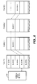
- FIGS. 1A and 1B are block diagrams of a non-volatile memory and a host system, respectively, that operate together.
- FIG. 2 illustrates a first example organization of the memory array of FIG. 1A .
- FIG. 3 shows an example host data sector with overhead data as stored in the memory array of FIG. 1A .
- FIG. 4 illustrates a second example organization of the memory array of FIG. 1A .
- FIG. 5 illustrates a third example organization of the memory array of FIG. 1A .
- FIG. 6 shows an extension of the third example organization of the memory array of FIG. 1A .
- FIG. 7 is a circuit diagram of a group of memory cells of the array of FIG. 1A in one particular configuration.
- FIG. 8 shows storage of sectors of data in a block of a memory array such as the memory array of FIG. 1A .
- FIG. 9 shows an alternative storage of sectors of data in a block of a memory array such as the memory array of FIG. 1A .
- FIG. 10A shows sectors of data of FIGS. 8 or 9 after copying to another block during a garbage collection operation.
- FIG. 10B shows sectors of data of FIG. 10A after copying to another block during a second garbage collection operation.
- FIG. 10C shows the block of FIG. 10B after more sectors of data are received.
- FIG. 11A shows an alternative storage arrangement using two erase blocks, an active block and a scratch pad block, to store the sectors of data of FIGS. 10A and 10B .
- FIG. 11B shows an alternative storage arrangement using two metablocks, an active block and a scratch pad block, to store sectors of data of FIGS. 10A and 10B .
- FIG. 12A shows two blocks, an active block and a scratch pad block, used to store sectors of data so that the sectors of data may be updated while stored without triggering a garbage collection operation.
- FIG. 12B shows an alternative storage system to that of FIG. 12A allowing all sectors of a page to be updated while stored without triggering a garbage collection.
- FIG. 12C shows another example of updating data using scratch pad block 1250 .
- FIG. 13 shows four threshold voltage ranges used to store two bits of data in a multi-level cell.
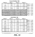
- FIG. 14 shows two blocks of multi-level cells, an active block and a scratch pad block, where the scratch pad block keeps a copy of a lower page of an active block.
- FIG. 15 shows sectors of data from two files stored in a block and the subsequent storage of the sectors of data when the two files are updated requiring more than one block of space in the memory array.
- FIG. 16 shows an alternative system of updating the sectors of data of FIG. 15 where a scratch pad block stores some sectors before they are copied to an active block.
- FIG. 17 shows a scratch pad block storing sectors of unrelated data in the same page and the subsequent copying of this data to different locations.
- FIG. 18 shows a scratch pad block storing sectors of unrelated data undergoing multiple updates.
- FIG. 19 shows a scratch pad block identified by a marking sector.
- FIG. 20 shows the scratch pad block of FIG. 19 storing a group of sectors and an index sector.
- FIG. 21 shows the scratch pad block of FIG. 20 storing a second group of sectors and a second index sector that supersedes the first index sector.
- FIG. 22 shows the scratch pad block of FIG. 21 storing a third group of sectors and a third index sector that supersedes the second index sector.
- FIG. 23 shows the scratch pad block of FIG. 22 with a fourth index sector that supersedes the third index sector when a group is copied to another block.
- a flash memory includes a memory cell array and a controller.
- two integrated circuit devices (chips) 11 and 13 include an array 15 of memory cells and various logic circuits 17 .
- the logic circuits 17 interface with a controller 19 on a separate chip through data, command and status circuits, and also provide addressing, data transfer and sensing, and other support to the array 13 .
- a number of memory array chips can be from one to many, depending upon the storage capacity provided.
- the controller and part or the entire array can alternatively be combined onto a single integrated circuit chip but this is currently not an economical alternative.
- a typical controller 19 includes a microprocessor 21 , a read-only-memory (ROM) 23 primarily to store firmware and a buffer memory (RAM) 25 primarily for the temporary storage of user data either being written to or read from the memory chips 11 and 13 .
- Circuits 27 interface with the memory array chip(s) and circuits 29 interface with a host though connections 31 . The integrity of data is in this example determined by calculating an ECC with circuits 33 dedicated to calculating the code. As user data is being transferred from the host to the flash memory array for storage, the circuit calculates an ECC from the data and the code is stored in the memory.
- connections 31 of the memory of FIG. 1A mate with connections 31 ′ of a host system, an example of which is given in FIG. 1B .
- Data transfers between the host and the memory of FIG. 1A are through interface circuits 35 .
- a typical host also includes a microprocessor 37 , a ROM 39 for storing firmware code and RAM 41 .
- Other circuits and subsystems 43 often include a high capacity magnetic data storage disk drive, interface circuits for a keyboard, a monitor and the like, depending upon the particular host system.
- hosts include desktop computers, laptop computers, handheld computers, palmtop computers, personal digital assistants (PDAs), MP3 and other audio players, digital cameras, video cameras, electronic game machines, wireless and wired telephony devices, answering machines, voice recorders, network routers and others.
- PDAs personal digital assistants
- MP3 and other audio players
- digital cameras digital cameras
- video cameras electronic game machines
- electronic game machines electronic game machines
- wireless and wired telephony devices answering machines
- voice recorders network routers and others.
- the memory of FIG. 1A may be implemented as a small enclosed card containing the controller and all its memory array circuit devices in a form that is removably connectable with the host of FIG. 1B . That is, mating connections 31 and 31 ′ allow a card to be disconnected and moved to another host, or replaced by connecting another card to the host.
- the memory array devices may be enclosed in a separate card that is electrically and mechanically connectable with a card containing the controller and connections 31 .
- the memory of FIG. 1A may be embedded within the host of FIG. 1B , wherein the connections 31 and 31 ′ are permanently made. In this case, the memory is usually contained within an enclosure of the host along with other components.
- FIG. 2 illustrates a portion of a memory array wherein memory cells are grouped into erase blocks, the cells in each erase block being erasable together as part of a single erase operation, usually simultaneously.
- An erase block is the minimum unit of erase in this type of memory.
- the size of the individual memory cell erase blocks of FIG. 2 can vary but one commercially practiced form includes a single sector of data in an individual erase block. The contents of such a data sector are illustrated in FIG. 3 .
- User data 51 are typically 512 bytes.
- overhead data that includes an ECC 53 calculated from the user data, parameters 55 relating to the sector data and/or the erase block in which the sector is programmed and an ECC 57 calculated from the parameters 55 and any other overhead data that might be included.
- One or more flags may also be included in the parameters 55 that indicate status or states. Indications of voltage levels to be used for programming and/or erasing the erase block can also be stored within the parameters 55 , these voltages being updated as the number of cycles experienced by the erase block and other factors change. Other examples of the parameters 55 include an identification of any defective cells within the erase block, the logical address of the erase block that is mapped into this physical erase block and the address of any substitute erase block in case the primary erase block is defective. The particular combination of parameters 55 that are used in any memory system will vary in accordance with the design. Also, some or all of the overhead data can be stored in erase blocks dedicated to such a function, rather than in the erase block containing the user data or to which the overhead data pertains.
- An example erase block 59 still the minimum unit of erase, contains four pages 0 - 3 , each of which is the minimum unit of programming.
- One or more host sectors of data are stored in each page, usually along with overhead data including at least the ECC calculated from the sector's data and may be in the form of the data sector of FIG. 3 .
- Re-writing the data of an entire block usually involves programming the new data into a block of an erase block pool, the original block then being erased and placed in the erase pool.
- the updated data are typically stored in a page of a block from the erased block pool and data in the remaining unchanged pages are copied from the original block into the new block.
- the original block is then erased.
- Variations of this large block management technique include writing the updated data into a page of another block without moving data from the original block or erasing it. This results in multiple pages having the same logical address.
- the most recent page of data is identified by some convenient technique such as the time of programming that is recorded as a field in sector or page overhead data.
- FIG. 5 A further multi-sector block arrangement is illustrated in FIG. 5 .
- the total memory cell array is physically divided into two or more planes, four planes 0 - 3 being illustrated.
- Each plane is a sub-array of memory cells that has its own data registers, sense amplifiers, addressing decoders and the like in order to be able to operate largely independently of the other planes. All the planes may be provided on a single integrated circuit device or on multiple devices, an example being to form each plane from one or more distinct integrated circuit devices.
- Each block in the example system of FIG. 5 contains 16 pages P 0 -P 15 , each page having a capacity of one, two or more host data sectors and some overhead data.
- FIG. 6 Yet another memory cell arrangement is illustrated in FIG. 6 .
- Each plane contains a large number of erase blocks of cells.
- erase blocks within different planes are logically linked to form metablocks.
- One such metablock is illustrated in FIG. 6 as being formed of erase block 3 of plane 0 , erase block 1 of plane 1 , erase block 1 of plane 2 and erase block 2 of plane 3 .
- Each metablock is logically addressable and the memory controller assigns and keeps track of the erase blocks that form the individual metablocks.
- the host system preferably interfaces with the memory system in units of data equal to the capacity of the individual metablocks.
- LBA logical block addresses
- PBNs physical block numbers
- All erase blocks of the metablock are erased together, and pages from each erase block are preferably programmed and read simultaneously.
- a metablock may be considered the unit of erase in a system in which erase blocks are linked in this way.
- pages may only be programmed in parallel with other pages of the metablock.
- a metapage is a minimum unit of programming of a metablock that consists of a page from each plane of the metablock.
- FIG. 7 One erase block of a memory array of the NAND type is shown in FIG. 7 .
- a large number of column oriented strings of series connected memory cells are connected between a common source 65 of a voltage V SS and one of bit lines BL 0 -BLN that are in turn connected with circuits 67 containing address decoders, drivers, read sense amplifiers and the like.
- one such string contains charge storage transistors 70 , 71 . . . 72 and 74 connected in series between select transistors 77 and 79 at opposite ends of the strings.
- each string contains 16 storage transistors but other numbers are possible.
- Word lines WL 0 -WL 15 extend across one storage transistor of each string and are connected to circuits 81 that contain address decoders and voltage source drivers of the word lines. Voltages on lines 83 and 84 control connection of all the strings in the erase block together to either the voltage source 65 and/or the bit lines BL 0 -BLN through their select transistors. Data and addresses come from the memory controller.
- Each row of charge storage transistors (memory cells) of the erase block may form a page that is programmed and read together.
- An appropriate voltage is applied to the word line (WL) of such a page for programming or reading its data while voltages applied to the remaining word lines are selected to render their respective storage transistors conductive.
- WL word line
- previously stored charge levels on unselected rows can be disturbed because of voltages applied across all the strings and to their word lines. This may prevent programming of cells of a particular row after other cells in the row have been programmed.
- Multiple state flash memories are particularly sensitive to disturbance. The increased number of logic states results in narrow threshold voltage ranges for individual states so that small changes in charge level may produce a change in logic state.
- sensitivity to disturbance increases.
- disturbance from subsequent programming of adjacent cells may define the page size.
- cells in a row may not be programmed subsequent to programming other cells in the same row, then the row defines the minimum unit of programming.
- a row of cells may contain one page of data. In such a memory array, if a group of cells in a row is programmed, the row is considered programmed even where some cells in the row contain no data. It is not efficient to have empty cells that cannot be subsequently programmed in the memory array.
- Empty cells in a programmed page may result from small numbers of sectors being received by the memory system at a time. For example, a single sector may be sent by a host to a memory system. The sector is stored in a page of the flash memory array. The sector prevents subsequent writing to that page. In a memory system in which a page holds multiple sectors, this may be inefficient. For example, where a page comprises four sectors of data, a portion of the memory array that could hold three sectors of data is left empty when a single sector is written to the page. As page sizes increase, the wasted space from such partially filled pages increases. Metapages may contain large numbers of sectors so storage may be particularly inefficient in memory arrays that use metablocks. The problem is similar where two or more sectors are received but the number of sectors received is less than the number of sectors in a page. Such partial pages may be stored in the scratch pad block until a full page of data is received.
- consolidation of stored data may be performed to combine data from partially filled pages into filled pages. This may be done as part of periodically performed garbage collection. Such consolidation of data copies data from the partially filled pages to full pages that are in a different erase block. The erase blocks that hold the partially filled pages are then marked as obsolete so that they may be erased and reused. Such an operation may take system resources that could be used for other functions.
- FIG. 8 shows an erase block, designated active block 800 of a memory array in a memory system in which a page is comprised of four sectors of data. Pages 0 - 5 are shown each extending in the horizontal direction. Each page may contain four sectors of data designated as sector 0 , sector 1 , sector 2 and sector 3 .
- a host sends single sectors of data to the memory system, which are stored in active block 800 .
- Sector X is received and stored as sector 0 of page 0 . This prevents subsequent programming of page 0 . Thus, sectors 1 , 2 and 3 of page 0 are not programmed and remain empty (erased).
- sector X+1 is received.
- Sector X+1 is stored as sector 0 of page 1 .
- Sectors 1 , 2 and 3 of page 1 remain empty.
- sector X+1 is programmed
- sector X+2 is received.
- Sector X+2 is stored as sector 0 of page 2 .
- Sectors 1 , 2 and 3 of page 2 remain empty.
- sector X+3 is received.
- Sector X+3 is stored as sector 0 of page 3 .
- Sectors 1 , 2 and 3 of page 3 remain empty.
- FIG. 9 shows an alternative way of storing sectors in an erase block, designated active block 900 .
- previously stored sectors are copied to a new page in the same erase block where they are stored with a more recently received sector.
- Sector X is stored as sector 0 of page 0 as before.
- sector X+1 is received and stored as sector 1 of page 1 with sector X copied from page 0 to sector 0 of page 1 .
- both sector X and sector X+1 are stored in page 1 .
- sector X+2 is received and stored as sector 2 of page 2 .
- Sector X is stored as sector 0 of page 2 and sector X+1 is stored as sector 1 of page 2 .
- sectors X, X+1 and X+2 are stored together in page 2 . Subsequently, sector X+3 is received and stored as sector 3 of page 3 .
- Sector X is stored as sector 0
- sector X+1 is stored as sector 1
- sector X+2 is stored as sector 2 of page 3 .
- four sectors of data are stored in page 3 so that page 3 is fully populated with data.
- FIGS. 8 or in FIG. 9 data may be consolidated.
- Sectors X, X+1, X+2 and X+3 of either FIG. 8 or FIG. 9 may be copied to a single page of a new erase block. This may be done as part of garbage collection at a time when it is convenient.
- FIG. 10A shows sectors X, X+1, X+2 and X+3 stored in page 0 of designated active block 1000 .
- Page 0 of erase block 1000 is filled with data.
- sector X+4 is received and is stored as sector 0 of page 1 of active block 1000 .
- sectors X+5, X+6 and X+7 are individually received and stored in pages 2 , 3 and 4 respectively. Consolidation of sectors may be needed again to consolidate sectors X+4, X+5, X+6 and X+7 to a single page. Such consolidation of sectors takes time during which host data may not be written. After the second consolidation of data to another erase block, erase block 1000 from which they are copied is marked as obsolete and may subsequently be erased.
- FIG. 10B shows an active block 1010 after the second garbage collection operation relocates data from the previous active block 1000 .
- Sectors X+4 to X+7 are consolidated into a single page (page 1 ) of active block 1010 .
- page 1 a single page of active block 1010 .
- more sectors may be received and may be stored in active block 1010 . If such sectors are received in the form of single sectors, a single sector may be stored in a page as before.
- FIG. 10C shows active block 1010 with additional sectors X+8 to X+11 stored in pages 2 - 5 .
- Another garbage collection operation may be needed to consolidate sectors X+8 to X+11 at this point.
- this method uses multiple garbage collection operations that require transferring data from one erase block to another erase block and erasing the first erase block. In larger erase blocks, the number of garbage collection operations is larger.
- a group of erase blocks may be linked so that they are erased together and programmed together. Data may be programmed in metapages containing many sectors. Therefore, storing single sectors becomes very inefficient because of the amount of garbage collection necessary.
- FIG. 11A shows an alternative method of storing data.
- FIG. 11A shows two erase blocks of a memory array.
- Active block 1110 is an erase block in which data may be programmed for long-term storage.
- Scratch pad block 1120 is an erase block in which data may be programmed for short-term storage. When small numbers of sectors are received, they are first stored in scratch pad block 1120 . Sectors continue to be stored in scratch pad block 1120 until enough sectors are received to fill a page of data. These sectors are then copied to a page of active block 1110 .
- Sector X is received and programmed as sector 0 of page 0 in scratch pad block 1120 as before. Subsequently, sector X+1 is received and stored as sector 1 of page. 1 of scratch pad block 1120 with sector X copied to sector 0 of page 1 . Subsequently, sector X+2 is received and stored as sector 2 of page 2 of scratch pad block 1120 with sectors X and X+1 stored as sector 0 and sector 1 of page 2 respectively. Subsequent to storing sector X+2 in scratch pad block 1120 , sector X+3 is received. At this point, sectors X, X+1, X+2 and X+3 are written to page 0 of active block 1110 . These four sectors form a full page of data.
- sectors X, X+1, X+2 and X+3 are efficiently stored in page 0 of active block 1110 .
- sectors X+4, X+5, X+6 and X+7 are individually received.
- Sectors X+4, X+5 and X+6 are stored in pages 3 , 4 and 5 of scratch pad block 1120 and are copied to sectors 0 , 1 and 2 of page 1 of active block 1110 when sector X+7 is received.
- Sector X+7 is programmed directly to sector 3 of page 1 of active block 1110 .
- scratch pad block 1120 has no available pages for storing data and may be designated as being ready for erase (obsolete).
- a new erase block may be designated as a scratch pad block for the next sector, or group of sectors, to be received. While this example shows single sectors being received, this method may also be used for groups of sectors where the group of sectors has fewer sectors than the number of sectors in a page. Also, while the above examples show writing data from a scratch pad block to an active block with maximum parallelism, such writing may be done with less than maximum parallelism and still provide an efficiency benefit. Thus, sectors are written to the scratch pad block with one degree of parallelism and subsequently written to another block with a higher degree of parallelism so that the data is more densely packed and requires less frequent garbage collection.
- a scratch pad block may also be used in memory arrays that use metablocks.
- FIG. 11B shows two metablocks, active block 1130 and scratch pad block 1140 .
- Both active block 1130 and scratch pad block 1140 have four planes, indicated as planes 0 - 3 . Each plane is one sector wide, so four sectors are stored in a metapage of block 1130 or 1140 .
- Both blocks have 6 metapages, indicated as metapage 0 - 5 .
- the technique for efficiently storing data is the same as that described above with respect to erase blocks. Sectors are accumulated in scratch pad block 1140 until a full metapage of data is available at which time a full metapage is programmed to active block 1130 .
- metapage 0 of active block 1130 when sector X+3 is received, a full metapage (sectors X, X+1, X+2 and X+3) is programmed to metapage 0 of active block 1130 .
- a metapage may have a large number of sectors because metablocks may have many planes and planes may be several pages wide. The technique described above is particularly valuable for such large metapages because of the large amount of space in the memory array that would otherwise be wasted.
- FIGS. 11A and 11B aspects of this invention described with respect to examples using erase block architecture may also be applied to metablock architecture and vice versa.
- the term “block” may indicate either an erase block or a metablock depending on the configuration of the memory array.
- a block is the unit of erase used in that configuration.
- the term “page” may refer to either a page within a single erase block or a metapage of a metablock. In either case, a page is the unit of programming for the configuration.
- sectors may be programmed directly to the active block of the memory array without first being stored in the scratch pad block.
- full pages of data may be programmed directly to the active block with a high degree of parallelism
- partial pages of data are programmed to the scratch pad block with a lower degree of parallelism until they may be written as part of a full-page program to the active block.
- a controller may determine the destination for a particular sector or group of sectors. Where writing a group of sectors to the active block would include both partial-page and full-page writes, the full-pages may be written to the active block and the partial page may be written to the scratch pad block.
- FIG. 12A shows a further example where sectors from a host are updated while they are stored in a scratch pad block.
- a first sector X 0 is received and stored in page 0 of scratch pad block 1250 .
- a page in this example stores four sectors of data.
- a replacement for X 0 shown as X 1 , is then received.
- the sectors in this example are numbered according to their logical address, with a subscript to indicate whether the sector is an update and if so, which version.
- sector X is a sector with logical address X and is the first updated version of this sector. This is a sector of data that has the same logical address as X 0 but may contain different data reflecting some updated information.
- Sector X 1 is written to page 1 of scratch pad block 1250 .
- the controller keeps track of which sectors are current and which are obsolete.
- scratch pad block 1250 the most recently written copy of a sector with a particular logical address is the current version. Any other version is obsolete.
- X 0 becomes obsolete when X 1 is programmed.
- sector (X+1) 0 is received. This is a sector that is logically sequential to sector X 1 . Both sectors X 1 and (X+1) 0 are written to page 2 . Subsequently, sector (X+1) 0 is replaced by (X+1) 1 . This is an updated version of sector (X+1) 0 that replaces sector (X+1) 0 .
- Sector (X+1) 1 is written to page 3 along with sector X 1 .
- sector (X+2) 0 is received and written to page 4 .
- Sector (X+2) 0 is subsequently replaced by sector (X+2) 1 and written to page 5 along with sectors X 1 and (X+1) 1 .
- sector (X+3) 0 is received.
- a page of data (sectors X 1 , (X+1) 1 , (X+2) 1 and (X+3) 0 ) are available.
- Sectors X 1 , (X+1) 1 , (X+2) 1 and (X+3) 0 are written to a block designated as active block 1252 .
- Sectors X 1 , (X+1) 1 , (X+2) 1 and (X+3) 0 are written to active block 1252 with parallelism of a full page write. This is the maximum possible parallelism in this case.
- sectors X 1 , (X+1) 1 , (X+2) 1 and (X+3) 0 were written to the scratch pad block 1250 with a low degree of parallelism, they are subsequently written to active block 1252 with a high degree of parallelism.
- sectors X 1 , (X+1) 1 , (X+2) 1 and (X+3) 0 are more efficiently stored in the active block. More efficient storage may result in garbage collection being necessary less frequently, thus improving performance.
- FIG. 12B An alternative example is provided in FIG. 12B .
- This example is similar to that shown in FIG. 12A but here sector (X+3) 0 is stored in scratch pad block 1250 prior to being copied to active block 1252 .
- This allows sector (X+3) 0 to be updated before it is written to active block 1252 .
- Sector (X+3) 0 is shown being updated by being replaced by sector (X+3) 1 .
- the complete page of data (sectors X 1 , (X+1) 1 , (X+2) 1 , and (X+3) 1 ) may be held in scratch pad block 1250 , ready to be updated, until some triggering event. In this case, sector (X+4) 0 is received, providing a triggering event.
- Sectors X 1 , (X+1) 1 , (X+2) 1 , and (X+3) 1 are written to active block 1252 at this point with maximum parallelism.
- Sector (X+4) 0 is written to the next available page (page 8 ) in scratch pad block 1250 .
- FIG. 12C shows another example of updating data using scratch pad block 1250 .
- Sectors of data X 0 to (X+15) 0 are stored in an original block 1254 .
- a host sends sector (X+6) 1 , which is an updated sector with the same logical address as sector (X+6) 0 .
- sector (X+6) 1 is to replace (X+6) 0 .
- page 1 of original block 1254 containing sectors (X+4) 0 to (X+7) 0
- sector (X+6) 1 is combined with sector (X+6) 1 and the combination is written to page 0 of scratch pad block 1250 .
- the updated page data may be kept in scratch pad block 1250 without writing it to an active block for some time.
- a subsequent updated sector (X+5) 1 is received from a host, the data may be updated in scratch pad block 1250 by writing sector (X+5) 1 along with copied sectors (X+4) 0 , (X+6) 1 , and (X+7) 0 to another page of scratch pad block 1250 (in this case, page 1 ).
- Multiple updates of a page of data in scratch pad block 1250 may be performed in this way.
- An update is carried out by replacing the updated sector or sectors of data and copying of unchanged sectors of data in a new page of scratch pad block 1250 .
- the copied sectors are copied within the same plane so that copying may be efficiently performed.
- the updated page of data may be copied to active block 1252 in the memory array.
- Non-sequential updates may be performed in this way without requiring a chaotic update block. For example, updated sectors (X+6) 1 and (X+5) 1 are received non-sequentially in the above example, but active block 1252 is sequential. Multiple pages of data may be held and updated at the same time in a scratch pad block in this way.
- a page may be copied to an active block when the page is no longer expected to be updated.
- FIG. 13 shows an example of how such multi-level cell (MLC) memories may be programmed to provide multiple threshold voltages that signify different logical states.
- MLC multi-level cell
- FIG. 13 represents the distribution of cell states With the number of cells represented on the vertical axis.
- Each threshold voltage A, B, C and D represents a different logical state.
- the four states represent two bits of data, one bit from a lower page of data and one bit from an upper page of data as indicated. In some examples, the lower page may be programmed first.
- FIG. 14 shows an example of how a scratch pad block 1460 may be used to reduce corruption of data in MLC memories.
- FIG. 14 shows both active block 1462 and scratch pad block 1460 as blocks of MLC memory. Pages of both blocks are numbered and shown as either “upper” or “lower” depending on which threshold voltage states are used to store the bits of data of the page.
- the memory first receives sectors X to X+3 and stores these sectors in lower page 0 of scratch pad block 1460 . Subsequently, the memory receives sectors X+4 to X+7. At this time, both the lower page (sectors X to X+3) and the upper page (X+4 to X+7) are written simultaneously to active block 1462 .
- the upper and lower pages may be written to an active block at different times but a copy of the lower page is kept in a scratch pad block in case the lower page in the active block becomes corrupted during programming of the upper page.
- sectors X to X+3 may be received and programmed to both the lower page 0 of active block 1462 and to lower page 0 of scratch pad block 1460 at the same time. Subsequently, sectors X+4 to X+7 are received and are programmed to upper page 0 of active block 1462 . Sectors X+4 to X+7 are not saved in scratch pad block 1460 .
- the data in lower page 0 of active block 1462 could be corrupted. That is, the threshold voltage of the cells being programmed could be modified so that they are no longer in a state representing data of the lower page but have not been fully programmed to a state representing data of the upper page. For example, a cell that is being programmed from state A in FIG. 13 to state D could be in state B or C at a time when programming stops. If data is corrupted in this manner the upper page of data that is being written may be recovered from the location from which it is being copied. However, in many cases, no other copy of the lower page exists. Here, a copy of the lower page is kept in scratch pad block 1460 until the programming of the upper page is completed. Thus, an uncorrupted copy of the lower page exists and may be used to recover the data of the lower page.
- FIG. 15 shows an example where page 0 to page i ⁇ 1 of original block 1570 contain data from a first file (file 1 ) and page i+1 to page n ⁇ 1 contain data from a second file (file 2 ).
- Page i contains sectors (i*4) and (i*4)+1 from file 1 and sectors (i*4)+2 and (i*4)+3 from file 2 .
- the sectors of file 2 are shaded to illustrate that sectors from two files are present.
- FIG. 15 shows file 2 being updated to a new block 1572 .
- the first page (page 0 ) of new block 1572 is written with the contents of page i of original block 1570 .
- page 0 of new block 1572 contains sectors from both file 2 and file 1 .
- Sectors (i*4) and (i*4)+1 from file 1 are not updated at this point but may be copied in order to program a full page of data.
- the remainder of updated file 2 is programmed to pages 1 to i ⁇ 1 of new block 1572 .
- file 1 is updated.
- Sector 0 to sector (i*4) ⁇ 1 are stored in page i to page n ⁇ 1. However, sectors (i*4) and (i*4)+1 are also part of file 1 and must be updated.
- new block 1572 is full at this point, the updated sectors (i*4) and (i*4)+1 are programmed to another block. Subsequently, sectors (i*4) and (i*4)+1 and the sectors in new block 1572 may be consolidated to a single block as part of a garbage collection operation. However, this takes time and system resources and is generally undesirable.
- FIG. 16 shows an alternative technique for updating sectors of original block 1570 of FIG. 15 that contains sectors from two different files.
- This technique uses a scratch pad block 1674 to store updated sectors until such time as they may be written as part of a full updated page with the maximum parallelism of the system.
- updated sectors (i*4)+2 and (i*4)+3 are written to scratch pad block 1674 .
- they are written to page 0 of scratch pad block 1674 and no data is written to the rest of the page so that a low degree of parallelism is used.
- the remaining sectors of file 2 (sectors (i*4)+4 to N ⁇ 1) are copied to pages 0 to n ⁇ i of a new block 1676 .
- Each page of new block 1676 is programmed with maximum parallelism to achieve maximum density of data in the block.
- Sectors (i*4)+2 and (i*4)+3 in scratch pad block 1674 may be marked as obsolete at this point.
- scratch pad block 1674 may be used for further operations without requiring a garbage collection operation because the scratch pad block routinely contains both current and obsolete data.
- sectors of data are written to the scratch pad block with a degree of parallelism that is less than that of writing a complete page.
- the remaining space in the page of the scratch pad block that is being written may remain empty because it is not possible to program it later without disturbing already-stored data.
- a memory system receives host data in single sectors or groups of sectors less than a page
- these sectors of host data may be stored in the scratch pad block in pages that also hold unrelated data such as unrelated host data or sectors of control data.
- sectors from the beginning of a file that are being stored in a scratch pad block for later storage as part of a full page may have additional sectors stored in the same scratch pad block page that are not logically related.
- FIG. 17 shows an example where sectors X, X+1 and X+2 are stored in a scratch pad block 1780 as in previous examples. However, here the remaining space in the pages of the scratch pad block holding sectors X, X+1 and X+2 are used to store other data.
- Sectors Y, Y+1 and Y+2 are stored with sector X in page 0 .
- Sectors Y, Y+1 and Y+2 may be logically unrelated to sectors X, X+1 and X+2. They may be from another host data file or from another cluster of sectors within the same file.
- Sectors Y, Y+1 and Y+2 may be non-sequential with sectors X, X+1 and X+2 and may be separated in logical address space.
- sectors Z and Z+1 are stored in page 1 with sectors X and X+1.
- Sectors Z and Z+1 may be logically unrelated to both sectors X, X+1 and X+2 and sectors Y, Y+1 and Y+2.
- Sectors X, X+1, X+2 and X+3 are subsequently written to a page of another block when sector X+3 is received.
- Sectors Y, Y+1, Y+2 and Y+3 are written to a page of another block when sector Y+3 is received.
- unrelated data may be stored in the same page of the scratch pad block to more efficiently use the available resources.
- FIG. 18 shows another example of unrelated data stored in a scratch pad block 1890 .
- sectors X, X+1 and X+2 are stored and updated as before.
- sector Y is also stored and updated in parallel. Updated sectors are denoted by a subscript indicating what version is stored.
- sector X 0 is the original version of sector X
- X 1 is the first updated version of sector X.
- Sector Y may be a sector of host data or a sector of control data that is frequently updated.
- control data such as FAT information is updated as host data is stored. Where small amounts of host data are received it may be advantageous to update the control data in scratch pad block 1890 . This may avoid updating a control structure where only a single sector of control data is updated. At some later time, the control data structures may be updated using control data from the scratch pad block.
- a scratch pad block may be a designated block in the memory array.
- a fixed physical location may be chosen as the scratch pad block. However, this may result in uneven wear of the memory array.
- the designated block may be changed from time to time so that as the scratch pad block becomes filled with obsolete data, another erase block is chosen as the scratch pad block.
- data structures used by the memory controller may identify the location of the scratch pad block or the designated scratch pad block may be marked so that if the controller scans the erase blocks of the memory array it may determine which erase block is the scratch pad block.
- a scratch pad block may be marked using a sector to identify it as a scratch pad block. For example, FIG. 19 shows marking sector 2110 as the first sector of scratch pad block 2100 .
- the erase blocks of the memory array may be scanned to determine the location of a scratch pad block or scratch pad blocks.
- the first sector of each erase block is read to see if it is a marking sector indicating a scratch pad block.
- Data may be written to a scratch pad block as a data group.
- a data group is a logically sequential group of sectors received from a host. When a data group is stored in the scratch pad block, an index sector is also written that provides information about the data group stored. The locations of the sectors of the data group may be stored in an index sector.
- a scratch pad block such as scratch pad block 2100 of FIG. 19 may be used to store multiple data groups.
- FIG. 20 shows scratch pad 2100 storing one data group.
- Data group 1 consists of two sectors 2220 , 2221 . These sectors, marking sector 2110 and an index sector 2230 are stored in scratch pad 2100 .
- Index sector 2230 stores information about group 1 .
- FIG. 21 shows scratch pad block 2100 of FIG. 20 after data group 2 consisting of two sectors 2340 , 2341 is programmed.
- Index sector 2350 is a new index sector that stores information about group 1 and group 2 .
- index sector 2230 is obsolete because index sector 2350 contains a complete record of the data groups of scratch pad block 2100 including group 1 .
- FIG. 22 shows scratch pad block 2100 of FIG. 21 after programming of data group 3 consisting of sectors 2460 , 2461 and 2462 .
- Index sector 2470 is a new index sector that stores information about data groups 1 , 2 and 3 .
- Index sector 2470 contains a complete record of the data of scratch pad block 2100 and thus makes index sector 2350 obsolete.
- FIG. 23 shows scratch pad block 2100 of FIG. 22 after data group 1 and data group 2 are read from scratch pad block 2100 and are written as a single page in another block of the memory array.
- Index sector 2560 stores information about data group 3 . Data group 1 and data group 2 in scratch pad 2100 are obsolete and do not require indexing because they are stored elsewhere. Thus, index sector 2560 contains a complete record of all current data in scratch pad block 2100 .
- a controller may first check if the requested sectors are in the scratch pad block. If the sectors are not present in the scratch pad block, the sectors may be sought in the regular manner. Thus, the scratch pad does not require changes to the regular media management used to keep track of the locations of sectors of data in the memory array.
Abstract
Description
Claims (22)
Priority Applications (34)
Application Number | Priority Date | Filing Date | Title |
---|---|---|---|
US11/016,285 US7315916B2 (en) | 2004-12-16 | 2004-12-16 | Scratch pad block |
US11/192,386 US7386655B2 (en) | 2004-12-16 | 2005-07-27 | Non-volatile memory and method with improved indexing for scratch pad and update blocks |
US11/191,686 US7412560B2 (en) | 2004-12-16 | 2005-07-27 | Non-volatile memory and method with multi-stream updating |
US11/192,220 US7366826B2 (en) | 2004-12-16 | 2005-07-27 | Non-volatile memory and method with multi-stream update tracking |
EP05852895.1A EP1828906B1 (en) | 2004-12-16 | 2005-12-01 | Scratch pad block |
PCT/US2005/043811 WO2006065566A1 (en) | 2004-12-16 | 2005-12-01 | Scratch pad block |
CN2005800422500A CN101095121B (en) | 2004-12-16 | 2005-12-01 | High speed temporary storage block |
JP2007546731A JP4787266B2 (en) | 2004-12-16 | 2005-12-01 | Scratch pad block |
KR1020077012082A KR100914263B1 (en) | 2004-12-16 | 2005-12-01 | Scratch pad block |
KR1020077014969A KR20070101261A (en) | 2004-12-16 | 2005-12-05 | Non-volatile memory and method with multi-stream update tracking |
JP2007546739A JP4399008B2 (en) | 2004-12-16 | 2005-12-05 | Non-volatile memory and method with multi-stream update tracking |
EP05853037.9A EP1834242B1 (en) | 2004-12-16 | 2005-12-05 | Non-volatile memory and method with multi-stream update tracking |
PCT/US2005/044001 WO2006065575A1 (en) | 2004-12-16 | 2005-12-05 | Non-volatile memory and method with multi-stream update tracking |
CNB200580047187XA CN100547565C (en) | 2004-12-16 | 2005-12-05 | The nonvolatile memory and the method for band multi-stream update tracking |
EP05848794.3A EP1834241B1 (en) | 2004-12-16 | 2005-12-07 | Non-volatile memory and method with improved indexing for scratch pad and update blocks |
KR1020077015222A KR101089576B1 (en) | 2004-12-16 | 2005-12-07 | Non-volatile memory and method with improved indexing for scratch pad and update blocks |
CNA2005800483896A CN101124556A (en) | 2004-12-16 | 2005-12-07 | Non-volatile memory and method with improved indexing for scratch pad and update blocks |
JP2007546776A JP2008524710A (en) | 2004-12-16 | 2005-12-07 | Non-volatile memory and method with improved indexing for scratchpads and update blocks |
PCT/US2005/044649 WO2006065655A1 (en) | 2004-12-16 | 2005-12-07 | Non-volatile memory and method with improved indexing for scratch pad and update blocks |
EP11001611A EP2336891A1 (en) | 2004-12-16 | 2005-12-08 | Non-volatile memory and method with multi-stream updating |
PCT/US2005/044720 WO2006065668A2 (en) | 2004-12-16 | 2005-12-08 | Non-volatile memory and method with multi-stream updating |
JP2007546782A JP4431175B2 (en) | 2004-12-16 | 2005-12-08 | Non-volatile memory and method with multi-stream update |
KR1020077015224A KR101202620B1 (en) | 2004-12-16 | 2005-12-08 | Non-volatile memory and method with multi-stream updating |
CN2005800473818A CN101124555B (en) | 2004-12-16 | 2005-12-08 | Non-volatile memory and method with multi-stream updating |
EP05853602.0A EP1839115B1 (en) | 2004-12-16 | 2005-12-08 | Non-volatile memory and method with multi-stream updating |
TW094144457A TWI393140B (en) | 2004-12-16 | 2005-12-15 | Methods of storing data in a non-volatile memory |
TW094144468A TWI417717B (en) | 2004-12-16 | 2005-12-15 | Non-volatile memory and method with multi-stream updating |
TW094144460A TW200636460A (en) | 2004-12-16 | 2005-12-15 | Non-volatile memory and method with multi-stream update tracking |
TW094144467A TWI394044B (en) | 2004-12-16 | 2005-12-15 | Non-volatile memory and method of recording data from a host |
IL183976A IL183976A0 (en) | 2004-12-16 | 2007-06-17 | Non-volatile memory and method with multi-stream update tracking |
IL183978A IL183978A0 (en) | 2004-12-16 | 2007-06-17 | Non-volatile memory and method with multi-stream updating |
IL183977A IL183977A0 (en) | 2004-12-16 | 2007-06-17 | Non-volatile memory and method with improved indexing for scratch pad and update blocks |
US12/189,396 US8151035B2 (en) | 2004-12-16 | 2008-08-11 | Non-volatile memory and method with multi-stream updating |
JP2009000562A JP5069256B2 (en) | 2004-12-16 | 2009-01-06 | Non-volatile memory and method with multi-stream update tracking |
Applications Claiming Priority (1)
Application Number | Priority Date | Filing Date | Title |
---|---|---|---|
US11/016,285 US7315916B2 (en) | 2004-12-16 | 2004-12-16 | Scratch pad block |
Related Child Applications (3)
Application Number | Title | Priority Date | Filing Date |
---|---|---|---|
US11/191,686 Continuation-In-Part US7412560B2 (en) | 2004-12-16 | 2005-07-27 | Non-volatile memory and method with multi-stream updating |
US11/192,220 Continuation-In-Part US7366826B2 (en) | 2004-12-16 | 2005-07-27 | Non-volatile memory and method with multi-stream update tracking |
US11/192,386 Continuation-In-Part US7386655B2 (en) | 2004-12-16 | 2005-07-27 | Non-volatile memory and method with improved indexing for scratch pad and update blocks |
Publications (2)
Publication Number | Publication Date |
---|---|
US20060161722A1 US20060161722A1 (en) | 2006-07-20 |
US7315916B2 true US7315916B2 (en) | 2008-01-01 |
Family
ID=36190514
Family Applications (1)
Application Number | Title | Priority Date | Filing Date |
---|---|---|---|
US11/016,285 Active 2025-12-17 US7315916B2 (en) | 2004-12-16 | 2004-12-16 | Scratch pad block |
Country Status (7)
Country | Link |
---|---|
US (1) | US7315916B2 (en) |
EP (1) | EP1828906B1 (en) |
JP (1) | JP4787266B2 (en) |
KR (1) | KR100914263B1 (en) |
CN (4) | CN101095121B (en) |
TW (1) | TWI393140B (en) |
WO (1) | WO2006065566A1 (en) |
Cited By (89)
Publication number | Priority date | Publication date | Assignee | Title |
---|---|---|---|---|
US20070214309A1 (en) * | 2006-03-07 | 2007-09-13 | Matsushita Electric Industrial Co., Ltd. | Nonvolatile storage device and data writing method thereof |
US20070271494A1 (en) * | 2006-05-17 | 2007-11-22 | Sandisk Corporation | Error Correction Coding for Multiple-Sector Pages in Flash Memory Devices |
US20070300130A1 (en) * | 2006-05-17 | 2007-12-27 | Sandisk Corporation | Method of Error Correction Coding for Multiple-Sector Pages in Flash Memory Devices |
US20080184086A1 (en) * | 2007-01-29 | 2008-07-31 | Sun Kwon Kim | Semiconductor memory system performing data error correction using flag cell array of buffer memory |
US20080301359A1 (en) * | 2004-12-16 | 2008-12-04 | Peter John Smith | Non-Volatile Memory and Method With Multi-Stream Updating |
US20090019218A1 (en) * | 2003-12-30 | 2009-01-15 | Alan Welsh Sinclair | Non-Volatile Memory And Method With Non-Sequential Update Block Management |
US20090070748A1 (en) * | 2007-09-12 | 2009-03-12 | Lin Jason T | Pointers for write abort handling |
US20090198895A1 (en) * | 2008-02-05 | 2009-08-06 | Via Technologies, Inc. | Control method, memory, and processing system utilizing the same |
US20100122114A1 (en) * | 2008-11-10 | 2010-05-13 | Ali Corporation | Data protection method for memory |
US20100146191A1 (en) * | 2007-12-05 | 2010-06-10 | Michael Katz | System and methods employing mock thresholds to generate actual reading thresholds in flash memory devices |
US20100257308A1 (en) * | 2009-04-07 | 2010-10-07 | Sandisk Corporation | Host stop-transmission handling |
US20100253555A1 (en) * | 2009-04-06 | 2010-10-07 | Hanan Weingarten | Encoding method and system, decoding method and system |
US20100277987A1 (en) * | 2009-04-30 | 2010-11-04 | Spansion Llc | Semiconductor device and control method thereof |
US20100293321A1 (en) * | 2009-05-12 | 2010-11-18 | Hanan Weingarten | Systems and method for flash memory management |
US20100318839A1 (en) * | 2009-06-16 | 2010-12-16 | Sandisk Corporation | Data recovery in multi-level cell nonvolatile memory |
US20110153919A1 (en) * | 2009-12-22 | 2011-06-23 | Erez Sabbag | Device, system, and method for reducing program/read disturb in flash arrays |
US20120233390A1 (en) * | 2008-10-16 | 2012-09-13 | Silicon Motion, Inc. | Data update method and flash memory apparatus utilizing the same |
US8724387B2 (en) | 2009-10-22 | 2014-05-13 | Densbits Technologies Ltd. | Method, system, and computer readable medium for reading and programming flash memory cells using multiple bias voltages |
US8730729B2 (en) | 2009-10-15 | 2014-05-20 | Densbits Technologies Ltd. | Systems and methods for averaging error rates in non-volatile devices and storage systems |
US8745317B2 (en) | 2010-04-07 | 2014-06-03 | Densbits Technologies Ltd. | System and method for storing information in a multi-level cell memory |
US8762800B1 (en) | 2008-01-31 | 2014-06-24 | Densbits Technologies Ltd. | Systems and methods for handling immediate data errors in flash memory |
US8782500B2 (en) | 2007-12-12 | 2014-07-15 | Densbits Technologies Ltd. | Systems and methods for error correction and decoding on multi-level physical media |
US8799563B2 (en) | 2007-10-22 | 2014-08-05 | Densbits Technologies Ltd. | Methods for adaptively programming flash memory devices and flash memory systems incorporating same |
US8819385B2 (en) | 2009-04-06 | 2014-08-26 | Densbits Technologies Ltd. | Device and method for managing a flash memory |
US20140258596A1 (en) * | 2013-03-11 | 2014-09-11 | Kabushiki Kaisha Toshiba | Memory controller and memory system |
WO2014137645A2 (en) | 2013-03-07 | 2014-09-12 | Sandisk Technologies Inc. | Write sequence providing write abort protection |
US8838937B1 (en) | 2012-05-23 | 2014-09-16 | Densbits Technologies Ltd. | Methods, systems and computer readable medium for writing and reading data |
US8850100B2 (en) | 2010-12-07 | 2014-09-30 | Densbits Technologies Ltd. | Interleaving codeword portions between multiple planes and/or dies of a flash memory device |
US8850297B1 (en) | 2010-07-01 | 2014-09-30 | Densbits Technologies Ltd. | System and method for multi-dimensional encoding and decoding |
US8879325B1 (en) | 2012-05-30 | 2014-11-04 | Densbits Technologies Ltd. | System, method and computer program product for processing read threshold information and for reading a flash memory module |
US8886877B1 (en) | 2014-05-15 | 2014-11-11 | Sandisk Technologies Inc. | In-situ block folding for nonvolatile memory |
US8902652B1 (en) | 2014-05-13 | 2014-12-02 | Sandisk Technologies Inc. | Systems and methods for lower page writes |
US8949515B2 (en) | 2009-12-03 | 2015-02-03 | Hitachi, Ltd. | Storage device and memory controller |
US8947941B2 (en) | 2012-02-09 | 2015-02-03 | Densbits Technologies Ltd. | State responsive operations relating to flash memory cells |
US8947817B1 (en) | 2014-04-28 | 2015-02-03 | Seagate Technology Llc | Storage system with media scratch pad |
US8964467B1 (en) | 2013-12-05 | 2015-02-24 | Sandisk Technologies Inc. | Systems and methods for partial page programming of multi level cells |
US8964464B2 (en) | 2010-08-24 | 2015-02-24 | Densbits Technologies Ltd. | System and method for accelerated sampling |
US8972675B2 (en) | 2013-06-27 | 2015-03-03 | Sandisk Technologies Inc. | Efficient post write read in three dimensional nonvolatile memory |
US8972472B2 (en) | 2008-03-25 | 2015-03-03 | Densbits Technologies Ltd. | Apparatus and methods for hardware-efficient unbiased rounding |
US8990665B1 (en) | 2011-04-06 | 2015-03-24 | Densbits Technologies Ltd. | System, method and computer program product for joint search of a read threshold and soft decoding |
US8996790B1 (en) | 2011-05-12 | 2015-03-31 | Densbits Technologies Ltd. | System and method for flash memory management |
US8996793B1 (en) | 2012-04-24 | 2015-03-31 | Densbits Technologies Ltd. | System, method and computer readable medium for generating soft information |
US8996788B2 (en) | 2012-02-09 | 2015-03-31 | Densbits Technologies Ltd. | Configurable flash interface |
US8995197B1 (en) | 2009-08-26 | 2015-03-31 | Densbits Technologies Ltd. | System and methods for dynamic erase and program control for flash memory device memories |
US9009398B2 (en) | 2013-07-02 | 2015-04-14 | Sandisk Technologies Inc. | Write operations for defect management in nonvolatile memory |
US9037902B2 (en) | 2013-03-15 | 2015-05-19 | Sandisk Technologies Inc. | Flash memory techniques for recovering from write interrupt resulting from voltage fault |
US9043537B1 (en) | 2013-11-21 | 2015-05-26 | Sandisk Technologies Inc. | Update block programming order |
US9063878B2 (en) | 2010-11-03 | 2015-06-23 | Densbits Technologies Ltd. | Method, system and computer readable medium for copy back |
US9063671B2 (en) | 2013-07-02 | 2015-06-23 | Sandisk Technologies Inc. | Write operations with full sequence programming for defect management in nonvolatile memory |
US9069659B1 (en) | 2013-01-03 | 2015-06-30 | Densbits Technologies Ltd. | Read threshold determination using reference read threshold |
US9110785B1 (en) | 2011-05-12 | 2015-08-18 | Densbits Technologies Ltd. | Ordered merge of data sectors that belong to memory space portions |
US9136876B1 (en) | 2013-06-13 | 2015-09-15 | Densbits Technologies Ltd. | Size limited multi-dimensional decoding |
US9182928B2 (en) | 2013-12-06 | 2015-11-10 | Sandisk Technologies Inc. | Lower page only host burst writes |
US9195592B1 (en) | 2011-05-12 | 2015-11-24 | Densbits Technologies Ltd. | Advanced management of a non-volatile memory |
US20150370491A1 (en) * | 2006-10-30 | 2015-12-24 | Samsung Electronics Co., Ltd. | Flash memory device with multi-level cells and method of writing data therein |
US9330767B1 (en) | 2009-08-26 | 2016-05-03 | Avago Technologies General Ip (Singapore) Pte. Ltd. | Flash memory module and method for programming a page of flash memory cells |
US9348694B1 (en) | 2013-10-09 | 2016-05-24 | Avago Technologies General Ip (Singapore) Pte. Ltd. | Detecting and managing bad columns |
US9368225B1 (en) | 2012-11-21 | 2016-06-14 | Avago Technologies General Ip (Singapore) Pte. Ltd. | Determining read thresholds based upon read error direction statistics |
US9372792B1 (en) | 2011-05-12 | 2016-06-21 | Avago Technologies General Ip (Singapore) Pte. Ltd. | Advanced management of a non-volatile memory |
US9396106B2 (en) | 2011-05-12 | 2016-07-19 | Avago Technologies General Ip (Singapore) Pte. Ltd. | Advanced management of a non-volatile memory |
US9397706B1 (en) | 2013-10-09 | 2016-07-19 | Avago Technologies General Ip (Singapore) Pte. Ltd. | System and method for irregular multiple dimension decoding and encoding |
US9407291B1 (en) | 2014-07-03 | 2016-08-02 | Avago Technologies General Ip (Singapore) Pte. Ltd. | Parallel encoding method and system |
US9413491B1 (en) | 2013-10-08 | 2016-08-09 | Avago Technologies General Ip (Singapore) Pte. Ltd. | System and method for multiple dimension decoding and encoding a message |
US20160239381A1 (en) * | 2015-02-17 | 2016-08-18 | Kabushiki Kaisha Toshiba | Memory system |
US9443553B2 (en) | 2014-04-28 | 2016-09-13 | Seagate Technology Llc | Storage system with multiple media scratch pads |
US9449702B1 (en) | 2014-07-08 | 2016-09-20 | Avago Technologies General Ip (Singapore) Pte. Ltd. | Power management |
US9501392B1 (en) | 2011-05-12 | 2016-11-22 | Avago Technologies General Ip (Singapore) Pte. Ltd. | Management of a non-volatile memory module |
US9524211B1 (en) | 2014-11-18 | 2016-12-20 | Avago Technologies General Ip (Singapore) Pte. Ltd. | Codeword management |
US9536612B1 (en) | 2014-01-23 | 2017-01-03 | Avago Technologies General Ip (Singapore) Pte. Ltd | Digital signaling processing for three dimensional flash memory arrays |
US9542262B1 (en) | 2014-05-29 | 2017-01-10 | Avago Technologies General Ip (Singapore) Pte. Ltd. | Error correction |
US9633233B2 (en) | 2014-05-07 | 2017-04-25 | Sandisk Technologies Llc | Method and computing device for encrypting data stored in swap memory |
US9665296B2 (en) | 2014-05-07 | 2017-05-30 | Sandisk Technologies Llc | Method and computing device for using both volatile memory and non-volatile swap memory to pre-load a plurality of applications |
US9710198B2 (en) | 2014-05-07 | 2017-07-18 | Sandisk Technologies Llc | Method and computing device for controlling bandwidth of swap operations |
US9786388B1 (en) | 2013-10-09 | 2017-10-10 | Avago Technologies General Ip (Singapore) Pte. Ltd. | Detecting and managing bad columns |
US9817593B1 (en) | 2016-07-11 | 2017-11-14 | Sandisk Technologies Llc | Block management in non-volatile memory system with non-blocking control sync system |
US9851921B1 (en) | 2015-07-05 | 2017-12-26 | Avago Technologies General Ip (Singapore) Pte. Ltd. | Flash memory chip processing |
US9858009B2 (en) | 2015-10-26 | 2018-01-02 | Sandisk Technologies Llc | Data folding in 3D nonvolatile memory |
US9892033B1 (en) | 2014-06-24 | 2018-02-13 | Avago Technologies General Ip (Singapore) Pte. Ltd. | Management of memory units |
US9921954B1 (en) | 2012-08-27 | 2018-03-20 | Avago Technologies General Ip (Singapore) Pte. Ltd. | Method and system for split flash memory management between host and storage controller |
US9928169B2 (en) | 2014-05-07 | 2018-03-27 | Sandisk Technologies Llc | Method and system for improving swap performance |
US9954558B1 (en) | 2016-03-03 | 2018-04-24 | Avago Technologies General Ip (Singapore) Pte. Ltd. | Fast decoding of data stored in a flash memory |
US9972393B1 (en) | 2014-07-03 | 2018-05-15 | Avago Technologies General Ip (Singapore) Pte. Ltd. | Accelerating programming of a flash memory module |
TWI625620B (en) * | 2017-05-12 | 2018-06-01 | 威盛電子股份有限公司 | Non-volatile memory apparatus and reading method thereof |
US10114562B2 (en) | 2014-09-16 | 2018-10-30 | Sandisk Technologies Llc | Adaptive block allocation in nonvolatile memory |
US10120792B1 (en) | 2014-01-29 | 2018-11-06 | Avago Technologies General Ip (Singapore) Pte. Ltd. | Programming an embedded flash storage device |
US10235284B2 (en) | 2017-03-23 | 2019-03-19 | Toshiba Memory Corporation | Memory system |
US10305515B1 (en) | 2015-02-02 | 2019-05-28 | Avago Technologies International Sales Pte. Limited | System and method for encoding using multiple linear feedback shift registers |
US10628255B1 (en) | 2015-06-11 | 2020-04-21 | Avago Technologies International Sales Pte. Limited | Multi-dimensional decoding |
US11573734B2 (en) | 2019-01-10 | 2023-02-07 | Silicon Motion, Inc. | Method for improving read-retry of flash memory and related controller and storage device |
Families Citing this family (54)
Publication number | Priority date | Publication date | Assignee | Title |
---|---|---|---|---|
US7173852B2 (en) * | 2003-10-03 | 2007-02-06 | Sandisk Corporation | Corrected data storage and handling methods |
US7366826B2 (en) | 2004-12-16 | 2008-04-29 | Sandisk Corporation | Non-volatile memory and method with multi-stream update tracking |
US7386655B2 (en) | 2004-12-16 | 2008-06-10 | Sandisk Corporation | Non-volatile memory and method with improved indexing for scratch pad and update blocks |
US7882299B2 (en) * | 2004-12-21 | 2011-02-01 | Sandisk Corporation | System and method for use of on-chip non-volatile memory write cache |
US7984084B2 (en) * | 2005-08-03 | 2011-07-19 | SanDisk Technologies, Inc. | Non-volatile memory with scheduled reclaim operations |
US7366017B2 (en) * | 2006-08-22 | 2008-04-29 | Micron Technology, Inc. | Method for modifying data more than once in a multi-level cell memory location within a memory array |
KR100849221B1 (en) * | 2006-10-19 | 2008-07-31 | 삼성전자주식회사 | Method for managing non-volatile memory, and memory-based apparatus including the non-volatile memory |
US8316206B2 (en) * | 2007-02-12 | 2012-11-20 | Marvell World Trade Ltd. | Pilot placement for non-volatile memory |
JP2008152464A (en) * | 2006-12-15 | 2008-07-03 | Toshiba Corp | Storage device |
US7917686B2 (en) | 2006-12-26 | 2011-03-29 | Sandisk Corporation | Host system with direct data file interface configurability |
US8209461B2 (en) | 2006-12-26 | 2012-06-26 | Sandisk Technologies Inc. | Configuration of host LBA interface with flash memory |
US7739444B2 (en) | 2006-12-26 | 2010-06-15 | Sandisk Corporation | System using a direct data file system with a continuous logical address space interface |
US8166267B2 (en) * | 2006-12-26 | 2012-04-24 | Sandisk Technologies Inc. | Managing a LBA interface in a direct data file memory system |
US8046522B2 (en) * | 2006-12-26 | 2011-10-25 | SanDisk Technologies, Inc. | Use of a direct data file system with a continuous logical address space interface and control of file address storage in logical blocks |
US9396103B2 (en) * | 2007-06-08 | 2016-07-19 | Sandisk Technologies Llc | Method and system for storage address re-mapping for a memory device |
KR20090024971A (en) * | 2007-09-05 | 2009-03-10 | 삼성전자주식회사 | Method and apparatus for cache using sector set |
JP5087347B2 (en) * | 2007-09-06 | 2012-12-05 | 株式会社日立製作所 | Semiconductor memory device and method for controlling semiconductor memory device |
US8296498B2 (en) * | 2007-11-13 | 2012-10-23 | Sandisk Technologies Inc. | Method and system for virtual fast access non-volatile RAM |
US20090164745A1 (en) * | 2007-12-21 | 2009-06-25 | Alan Sinclair | System and Method for Controlling an Amount of Unprogrammed Capacity in Memory Blocks of a Mass Storage System |
EP2592551A3 (en) | 2008-03-11 | 2013-08-28 | Agere System Inc. | Methods and apparatus for storing data in a multi-level cell flash memory device with cross-page sectors, multi-page coding and per-page coding |
US8452940B2 (en) * | 2008-12-30 | 2013-05-28 | Sandisk Technologies Inc. | Optimized memory management for random and sequential data writing |
WO2011021367A1 (en) * | 2009-08-21 | 2011-02-24 | パナソニック株式会社 | Non-volatile storage device, access device, and non-volatile storage system |
JP4956593B2 (en) | 2009-09-08 | 2012-06-20 | 株式会社東芝 | Memory system |
TWI399644B (en) * | 2009-12-24 | 2013-06-21 | Univ Nat Taiwan | Block management method for a non-volatile memory |
JP5330549B2 (en) * | 2010-02-02 | 2013-10-30 | 株式会社東芝 | Communication device with storage function |
US8345482B2 (en) * | 2010-12-15 | 2013-01-01 | Micron Technology, Inc. | Methods for segmented programming and memory devices |
TWI479505B (en) * | 2010-12-16 | 2015-04-01 | Phison Electronics Corp | Data management method, memory controller and memory storage apparatus |
CN103092771A (en) * | 2011-10-31 | 2013-05-08 | 建兴电子科技股份有限公司 | Solid-state storing device and control method of cache thereof |
TWI470575B (en) * | 2011-11-24 | 2015-01-21 | Mediatek Inc | Method for read pointer maintenance of a buffering apparatus, buffer controller and buffer apparatus |
CN103138875B (en) * | 2011-11-28 | 2015-06-10 | 澜起科技(上海)有限公司 | Calibration method of high-speed broadcast channel |
DE102012201978A1 (en) * | 2012-02-10 | 2013-08-14 | Robert Bosch Gmbh | Method for reading out a light sensor control device and device for reading out a light sensor control device |
CN103258570B (en) * | 2012-02-15 | 2016-05-11 | 旺宏电子股份有限公司 | A kind of method of memory storage and generating routine bias pulse and integrated circuit |
CN104081357A (en) * | 2012-04-27 | 2014-10-01 | 惠普发展公司,有限责任合伙企业 | Local checkpointing using a multi-level cell |
JP2013229086A (en) * | 2012-04-27 | 2013-11-07 | Sony Corp | Memory device, memory control device, and memory control method |
US9053003B2 (en) * | 2012-06-21 | 2015-06-09 | Microsoft Technology Licensing, Llc | Memory compaction mechanism for main memory databases |
CN102831072B (en) * | 2012-08-10 | 2016-03-02 | 深圳市江波龙电子有限公司 | Flash memory device and management method, data read-write method and read-write equipment |
US9478271B2 (en) * | 2013-03-14 | 2016-10-25 | Seagate Technology Llc | Nonvolatile memory data recovery after power failure |
CN104423888B (en) * | 2013-08-23 | 2017-10-03 | 群联电子股份有限公司 | Method for writing data, memorizer control circuit unit and memory storage apparatus |
CN104731710B (en) * | 2013-12-18 | 2018-06-29 | 群联电子股份有限公司 | Storage management method, memorizer control circuit unit and memorizer memory devices |
JP6412820B2 (en) * | 2015-03-31 | 2018-10-24 | 株式会社メガチップス | Storage system, control device, memory control device, storage device, host device, control program, and data reading method |
CN105159601B (en) * | 2015-08-07 | 2018-12-07 | 杭州海兴电力科技股份有限公司 | A method of improving Flash erasing and writing life |
KR102441284B1 (en) * | 2016-01-12 | 2022-09-08 | 에스케이하이닉스 주식회사 | Memory system and operating method of memory system |
JP7089505B2 (en) * | 2016-08-26 | 2022-06-22 | サンライズ メモリー コーポレイション | Capacitively coupled non-volatile thin film transistor string in a 3D array |
CN106528441B (en) * | 2016-10-26 | 2020-08-04 | 珠海格力电器股份有限公司 | Data processing method and device for simulating EEPROM (electrically erasable programmable read-Only memory) and electronic equipment |
CN111897498A (en) * | 2018-07-27 | 2020-11-06 | 创新先进技术有限公司 | Multi-level storage method and device for block chain data |
CN109215171A (en) * | 2018-08-20 | 2019-01-15 | 深圳市长龙铁路电子工程有限公司 | A kind of storage method of cab signaling equipment data record |
CN110888591B (en) * | 2018-09-07 | 2023-05-30 | 慧荣科技股份有限公司 | Data storage device and non-volatile memory control method |
CN110888820B (en) | 2018-09-07 | 2022-01-25 | 慧荣科技股份有限公司 | Data storage device and non-volatile memory control method |
CN110888593B (en) | 2018-09-07 | 2024-01-26 | 慧荣科技股份有限公司 | Data storage device and non-volatile memory control method |
TWI718889B (en) * | 2019-01-10 | 2021-02-11 | 慧榮科技股份有限公司 | Method for improving read retry of flash memory and related controller and storage device |
CN111400302B (en) * | 2019-11-28 | 2023-09-19 | 杭州海康威视系统技术有限公司 | Modification method, device and system for continuous storage data |
TWI727842B (en) | 2020-02-20 | 2021-05-11 | 大陸商長江存儲科技有限責任公司 | Memory device and programming method thereof |
JP2022542990A (en) | 2020-04-23 | 2022-10-07 | 長江存儲科技有限責任公司 | Memory device and programming method |
CN114911426B (en) * | 2022-07-15 | 2022-10-18 | 北谷电子有限公司 | Data storage method, storage device and overhead truck |
Citations (98)
Publication number | Priority date | Publication date | Assignee | Title |
---|---|---|---|---|
US4139911A (en) | 1978-03-13 | 1979-02-13 | Westinghouse Electric Corp. | High speed sense circuit for semiconductor memories |
US4218764A (en) | 1978-10-03 | 1980-08-19 | Matsushita Electric Industrial Co., Ltd. | Non-volatile memory refresh control circuit |
US4253059A (en) | 1979-05-14 | 1981-02-24 | Fairchild Camera & Instrument Corp. | EPROM Reliability test circuit |
US4460982A (en) | 1982-05-20 | 1984-07-17 | Intel Corporation | Intelligent electrically programmable and electrically erasable ROM |
US4612630A (en) | 1984-07-27 | 1986-09-16 | Harris Corporation | EEPROM margin testing design |
US4694454A (en) | 1984-07-27 | 1987-09-15 | Hitachi, Ltd. | Dynamic memory diagnosis and error correction apparatus |
US4703453A (en) | 1982-02-15 | 1987-10-27 | Hitachi, Ltd. | Semiconductor memory with an improved dummy cell arrangement and with a built-in error correcting code circuit |
US4703196A (en) | 1984-08-13 | 1987-10-27 | Fujitsu Limited | High voltage precharging circuit |
US4733394A (en) | 1985-04-23 | 1988-03-22 | Deutsche Itt Industries Gmbh | Electrically programmable semiconductor memory showing redundance |
US4763305A (en) | 1985-11-27 | 1988-08-09 | Motorola, Inc. | Intelligent write in an EEPROM with data and erase check |
US4779272A (en) | 1985-11-13 | 1988-10-18 | Mitsubishi Denki Kabushiki Kaisha | Testable variable-threshold non-volatile semiconductor memory |
US4799195A (en) | 1985-01-26 | 1989-01-17 | Kabushiki Kaisha Toshiba | Semiconductor memory device with a sense amplifier |
US4809231A (en) | 1987-11-12 | 1989-02-28 | Motorola, Inc. | Method and apparatus for post-packaging testing of one-time programmable memories |
US4827450A (en) | 1987-07-21 | 1989-05-02 | Sgs-Thomson Microelectronics S.A. | Integrated circuit with memory comprising a fraud-prevention device |
US4937787A (en) | 1987-06-30 | 1990-06-26 | Nec Corporation | Programmable read only memory with means for discharging bit line before program verifying operation |
US4962322A (en) | 1988-12-05 | 1990-10-09 | Texas Instruments Incorporated | Nonvolatible capacitor random access memory |
US4964079A (en) | 1988-04-26 | 1990-10-16 | Sgs-Thomson Microelectronics | Electrically programmable memory with several information bits per cell |
US5043940A (en) | 1988-06-08 | 1991-08-27 | Eliyahou Harari | Flash EEPROM memory systems having multistate storage cells |
US5065364A (en) | 1989-09-15 | 1991-11-12 | Intel Corporation | Apparatus for providing block erasing in a flash EPROM |
US5070032A (en) | 1989-03-15 | 1991-12-03 | Sundisk Corporation | Method of making dense flash eeprom semiconductor memory structures |
US5095344A (en) | 1988-06-08 | 1992-03-10 | Eliyahou Harari | Highly compact eprom and flash eeprom devices |
US5119330A (en) | 1989-03-31 | 1992-06-02 | Oki Electric Industry Co, Ltd. | Nonvolatile memory system for multiple value storing |
US5122985A (en) | 1990-04-16 | 1992-06-16 | Giovani Santin | Circuit and method for erasing eeprom memory arrays to prevent over-erased cells |
US5132935A (en) | 1990-04-16 | 1992-07-21 | Ashmore Jr Benjamin H | Erasure of eeprom memory arrays to prevent over-erased cells |
US5151906A (en) | 1989-05-25 | 1992-09-29 | Rohm Co., Ltd. | Semiconductor memory device having self-correcting function |
US5157629A (en) | 1985-11-22 | 1992-10-20 | Hitachi, Ltd. | Selective application of voltages for testing storage cells in semiconductor memory arrangements |
US5172338A (en) | 1989-04-13 | 1992-12-15 | Sundisk Corporation | Multi-state EEprom read and write circuits and techniques |
US5200959A (en) | 1989-10-17 | 1993-04-06 | Sundisk Corporation | Device and method for defect handling in semi-conductor memory |
US5200922A (en) | 1990-10-24 | 1993-04-06 | Rao Kameswara K | Redundancy circuit for high speed EPROM and flash memory devices |
US5239505A (en) | 1990-12-28 | 1993-08-24 | Intel Corporation | Floating gate non-volatile memory with blocks and memory refresh |
US5263032A (en) | 1991-06-27 | 1993-11-16 | Digital Equipment Corporation | Computer system operation with corrected read data function |
US5262984A (en) | 1988-07-29 | 1993-11-16 | Mitsubishi Denki Kabushiki Kaisha | Non-volatile memory device capable of storing multi-state data |
US5270551A (en) | 1990-02-14 | 1993-12-14 | Hitachi, Ltd. | Method of and apparatus for protecting electronic circuit against radiation |
US5270979A (en) | 1991-03-15 | 1993-12-14 | Sundisk Corporation | Method for optimum erasing of EEPROM |
US5278794A (en) | 1991-10-14 | 1994-01-11 | Kabushiki Kaisha Toshiba | NAND-cell type electrically erasable and programmable read-only memory with redundancy circuit |
US5313427A (en) | 1991-09-20 | 1994-05-17 | Texas Instruments Incorporated | EEPROM array with narrow margin of voltage thresholds after erase |
US5313421A (en) | 1992-01-14 | 1994-05-17 | Sundisk Corporation | EEPROM with split gate source side injection |
US5315421A (en) | 1992-04-28 | 1994-05-24 | Matsushita Electric Industrial Co., Ltd. | Rubbing apparatus including double refraction phase difference measuring means and manufacturing method for liquid crystal display device |
US5321655A (en) | 1989-06-12 | 1994-06-14 | Kabushiki Kaisha Toshiba | Semiconductor memory device |
US5327383A (en) | 1992-04-21 | 1994-07-05 | Intel Corporation | Method and circuitry for erasing a nonvolatile semiconductor memory incorporating row redundancy |
US5335198A (en) | 1993-05-06 | 1994-08-02 | Advanced Micro Devices, Inc. | Flash EEPROM array with high endurance |
US5341334A (en) | 1992-09-02 | 1994-08-23 | Kabushiki Kaisha Toshiba | Level shifter circuit constituted of E and I type transistors and an EEPROM using the same |
US5343063A (en) | 1990-12-18 | 1994-08-30 | Sundisk Corporation | Dense vertical programmable read only memory cell structure and processes for making them |
US5347489A (en) | 1992-04-21 | 1994-09-13 | Intel Corporation | Method and circuitry for preconditioning shorted rows in a nonvolatile semiconductor memory incorporating row redundancy |
US5365486A (en) | 1992-12-16 | 1994-11-15 | Texas Instruments Incorporated | Method and circuitry for refreshing a flash electrically erasable, programmable read only memory |
US5394359A (en) | 1989-07-20 | 1995-02-28 | Gemplus Card International | MOS integrated circuit with adjustable threshold voltage |
US5404485A (en) | 1993-03-08 | 1995-04-04 | M-Systems Flash Disk Pioneers Ltd. | Flash file system |
US5465236A (en) | 1992-06-19 | 1995-11-07 | Kabushiki Kaisha Toshiba | Nonvolatile semiconductor memory system with a plurality of erase blocks |
US5475693A (en) | 1994-12-27 | 1995-12-12 | Intel Corporation | Error management processes for flash EEPROM memory arrays |
US5504760A (en) | 1991-03-15 | 1996-04-02 | Sandisk Corporation | Mixed data encoding EEPROM system |
US5523972A (en) | 1994-06-02 | 1996-06-04 | Intel Corporation | Method and apparatus for verifying the programming of multi-level flash EEPROM memory |
US5532962A (en) | 1992-05-20 | 1996-07-02 | Sandisk Corporation | Soft errors handling in EEPROM devices |
US5570315A (en) | 1993-09-21 | 1996-10-29 | Kabushiki Kaisha Toshiba | Multi-state EEPROM having write-verify control circuit |
US5583812A (en) | 1988-06-08 | 1996-12-10 | Harari; Eliyahou | Flash EEPROM system cell array with more than two storage states per memory cell |
US5598370A (en) | 1993-02-24 | 1997-01-28 | International Business Machines Corporation | Nonvolatile memory with cluster-erase flash capability and solid state file apparatus using the same |
US5648934A (en) | 1995-02-13 | 1997-07-15 | Micron Technology, Inc. | On-chip memory redundancy circuitry for programmable non-volatile memories, and methods for programming same |
US5652720A (en) | 1994-12-20 | 1997-07-29 | Sgs-Thomson Microelectronics S.A. | Electrically programmable memory with improved retention of data and a method of writing data in said memory |
US5657332A (en) | 1992-05-20 | 1997-08-12 | Sandisk Corporation | Soft errors handling in EEPROM devices |
US5661053A (en) | 1994-05-25 | 1997-08-26 | Sandisk Corporation | Method of making dense flash EEPROM cell array and peripheral supporting circuits formed in deposited field oxide with the use of spacers |
US5675537A (en) | 1996-08-22 | 1997-10-07 | Advanced Micro Devices, Inc. | Erase method for page mode multiple bits-per-cell flash EEPROM |
US5689465A (en) | 1992-06-19 | 1997-11-18 | Texas Instruments Incorporated | Semiconductor memory device and defective memory cell correction circuit |
US5696929A (en) | 1995-10-03 | 1997-12-09 | Intel Corporation | Flash EEPROM main memory in a computer system |
US5699297A (en) | 1995-05-30 | 1997-12-16 | Kabushiki Kaisha Toshiba | Method of rewriting data in a microprocessor additionally provided with a flash memory |
US5703506A (en) | 1995-12-26 | 1997-12-30 | Motorola | Signal processing method |
US5712815A (en) | 1996-04-22 | 1998-01-27 | Advanced Micro Devices, Inc. | Multiple bits per-cell flash EEPROM capable of concurrently programming and verifying memory cells and reference cells |
US5717632A (en) | 1996-11-27 | 1998-02-10 | Advanced Micro Devices, Inc. | Apparatus and method for multiple-level storage in non-volatile memories |
US5751639A (en) | 1995-01-20 | 1998-05-12 | Kabushiki Kaisha Toshiba | DRAM having a power supply voltage lowering circuit |
US5761125A (en) | 1994-08-10 | 1998-06-02 | Kabushiki Kaisha Toshiba | Cell threshold value distribution detection circuit and method of detecting cell threshold value |
US5774397A (en) | 1993-06-29 | 1998-06-30 | Kabushiki Kaisha Toshiba | Non-volatile semiconductor memory device and method of programming a non-volatile memory cell to a predetermined state |
US5798968A (en) | 1996-09-24 | 1998-08-25 | Sandisk Corporation | Plane decode/virtual sector architecture |
US5835413A (en) | 1996-12-20 | 1998-11-10 | Intel Corporation | Method for improved data retention in a nonvolatile writeable memory by sensing and reprogramming cell voltage levels |
US5835927A (en) | 1993-06-30 | 1998-11-10 | Intel Corporation | Special test modes for a page buffer shared resource in a memory device |
US5860091A (en) | 1996-06-28 | 1999-01-12 | Symbios, Inc. | Method and apparatus for efficient management of non-aligned I/O write request in high bandwidth raid applications |
US5890192A (en) | 1996-11-05 | 1999-03-30 | Sandisk Corporation | Concurrent write of multiple chunks of data into multiple subarrays of flash EEPROM |
US5905673A (en) | 1995-10-06 | 1999-05-18 | Agate Semiconductor, Inc. | Integrated circuit for storage and retrieval of multiple digital bits per nonvolatile memory cell |
US5909449A (en) | 1997-09-08 | 1999-06-01 | Invox Technology | Multibit-per-cell non-volatile memory with error detection and correction |
US5930167A (en) | 1997-07-30 | 1999-07-27 | Sandisk Corporation | Multi-state non-volatile flash memory capable of being its own two state write cache |
US5933368A (en) | 1996-11-25 | 1999-08-03 | Macronix International Co., Ltd. | Flash memory mass storage system |
US5937425A (en) | 1997-10-16 | 1999-08-10 | M-Systems Flash Disk Pioneers Ltd. | Flash file system optimized for page-mode flash technologies |
US5963473A (en) | 1996-05-23 | 1999-10-05 | Micron Technology, Inc. | Flash memory system and method for monitoring the disturb effect on memory cell blocks due to high voltage conditions of other memory cell blocks |
US6046935A (en) | 1996-03-18 | 2000-04-04 | Kabushiki Kaisha Toshiba | Semiconductor device and memory system |
US6125435A (en) | 1995-09-13 | 2000-09-26 | Lexar Media, Inc. | Alignment of cluster address to block addresses within a semiconductor non-volatile mass storage memory |
US6145051A (en) | 1995-07-31 | 2000-11-07 | Lexar Media, Inc. | Moving sectors within a block of information in a flash memory mass storage architecture |
US6189081B1 (en) | 1996-05-24 | 2001-02-13 | Nec Corporation | Non-volatile semiconductor storage with memory requirement and availability comparison means and method |
US6199139B1 (en) | 1998-01-27 | 2001-03-06 | International Business Machines Corporation | Refresh period control apparatus and method, and computer |
US6222762B1 (en) | 1992-01-14 | 2001-04-24 | Sandisk Corporation | Multi-state memory |
US6262918B1 (en) | 1999-04-01 | 2001-07-17 | Lexar Media, Inc. | Space management for managing high capacity nonvolatile memory |
US6345001B1 (en) | 2000-09-14 | 2002-02-05 | Sandisk Corporation | Compressed event counting technique and application to a flash memory system |
US6415352B1 (en) | 1999-02-24 | 2002-07-02 | Sanyo Electric Co., Ltd. | One-chip microcomputer and method of refreshing its data |
US6426893B1 (en) | 2000-02-17 | 2002-07-30 | Sandisk Corporation | Flash eeprom system with simultaneous multiple data sector programming and storage of physical block characteristics in other designated blocks |
US6434658B1 (en) | 1999-04-05 | 2002-08-13 | Mitsubishi Denki Kabushiki Kaisha | Memory device operable with a small-capacity buffer memory and having a flash memory |
US6456528B1 (en) | 2001-09-17 | 2002-09-24 | Sandisk Corporation | Selective operation of a multi-state non-volatile memory system in a binary mode |
US6459644B2 (en) | 2000-06-06 | 2002-10-01 | Hitachi, Ltd. | Semiconductor memory device with block alignment function |
US6522580B2 (en) | 2001-06-27 | 2003-02-18 | Sandisk Corporation | Operating techniques for reducing effects of coupling between storage elements of a non-volatile memory operated in multiple data states |
US6560152B1 (en) | 2001-11-02 | 2003-05-06 | Sandisk Corporation | Non-volatile memory with temperature-compensated data read |
US6567307B1 (en) * | 2000-07-21 | 2003-05-20 | Lexar Media, Inc. | Block management for mass storage |
US20050235098A1 (en) * | 2004-02-04 | 2005-10-20 | Kazuaki Tamura | Semiconductor memory device, memory controller and memory access device |
US20070005829A1 (en) * | 2004-11-12 | 2007-01-04 | Akihisa Fujimoto | Memory card having memory element and card controller thereof |
Family Cites Families (30)
Publication number | Priority date | Publication date | Assignee | Title |
---|---|---|---|---|
US7190617B1 (en) * | 1989-04-13 | 2007-03-13 | Sandisk Corporation | Flash EEprom system |
FR2689253B1 (en) * | 1992-03-24 | 1997-01-24 | Souriau & Cie | MOLDING DEVICE COMPRISING A PIN GUIDE COUNTERPIECE FOR MOLDING FIBER OPTIC CONNECTOR BOLTS, AND MOLDED BUCKLE USING SUCH A DEVICE. |
GB9208493D0 (en) * | 1992-04-16 | 1992-06-03 | Thomson Consumer Electronics | Dual port video memory |
JP3088866B2 (en) * | 1992-11-26 | 2000-09-18 | 大日本印刷株式会社 | IC card |
JP3866818B2 (en) * | 1997-02-14 | 2007-01-10 | 三菱電機株式会社 | Semiconductor memory device |
GB9903490D0 (en) * | 1999-02-17 | 1999-04-07 | Memory Corp Plc | Memory system |
US6725322B1 (en) * | 1999-02-22 | 2004-04-20 | Renesas Technology Corp. | Memory card, method for allotting logical address, and method for writing data |
JP3793868B2 (en) * | 1999-11-25 | 2006-07-05 | カシオ計算機株式会社 | Flash memory management device and recording medium |
WO2001084321A1 (en) * | 2000-05-04 | 2001-11-08 | Koninklijke Philips Electronics N.V. | Method, system and computer program for data management on storage medium |
US6772274B1 (en) * | 2000-09-13 | 2004-08-03 | Lexar Media, Inc. | Flash memory system and method implementing LBA to PBA correlation within flash memory array |
US6763424B2 (en) * | 2001-01-19 | 2004-07-13 | Sandisk Corporation | Partial block data programming and reading operations in a non-volatile memory |
JP3979486B2 (en) * | 2001-09-12 | 2007-09-19 | 株式会社ルネサステクノロジ | Nonvolatile storage device and data storage method |
GB0123412D0 (en) * | 2001-09-28 | 2001-11-21 | Memquest Ltd | Memory system sectors |
US6678785B2 (en) * | 2001-09-28 | 2004-01-13 | M-Systems Flash Disk Pioneers Ltd. | Flash management system using only sequential write |
US6925007B2 (en) * | 2001-10-31 | 2005-08-02 | Sandisk Corporation | Multi-state non-volatile integrated circuit memory systems that employ dielectric storage elements |
ATE402999T1 (en) * | 2002-01-17 | 2008-08-15 | Univ British Columbia | BISPECIFIC ANTISENSE OLIGONUCLEOTIDES THAT INHIBIT IGFBP-2 AND IGFBP-5 AND THEIR USE |
JP4206688B2 (en) * | 2002-04-15 | 2009-01-14 | ソニー株式会社 | Data processing apparatus and data processing method |
KR100453053B1 (en) * | 2002-06-10 | 2004-10-15 | 삼성전자주식회사 | Flash memory file system |
US7196931B2 (en) * | 2002-09-24 | 2007-03-27 | Sandisk Corporation | Non-volatile memory and method with reduced source line bias errors |
CN100483552C (en) * | 2002-10-28 | 2009-04-29 | 桑迪士克股份有限公司 | Automated wear leveling in non-volatile storage systems |
JP4073799B2 (en) * | 2003-02-07 | 2008-04-09 | 株式会社ルネサステクノロジ | Memory system |
JP3928724B2 (en) * | 2003-02-20 | 2007-06-13 | ソニー株式会社 | Recording medium recording control method and recording medium recording control apparatus |
US6928511B2 (en) * | 2003-03-03 | 2005-08-09 | High Tech Computer, Corp. | Method and system for managing virtual memory |
EP1489490A3 (en) * | 2003-06-19 | 2005-09-14 | Texas Instruments Incorporated | Method for converting a cache to a scratch-pad memory |
US7433993B2 (en) * | 2003-12-30 | 2008-10-07 | San Disk Corportion | Adaptive metablocks |
US7139864B2 (en) * | 2003-12-30 | 2006-11-21 | Sandisk Corporation | Non-volatile memory and method with block management system |
US8504798B2 (en) * | 2003-12-30 | 2013-08-06 | Sandisk Technologies Inc. | Management of non-volatile memory systems having large erase blocks |
US20050144363A1 (en) * | 2003-12-30 | 2005-06-30 | Sinclair Alan W. | Data boundary management |
JP4713867B2 (en) * | 2004-09-22 | 2011-06-29 | 株式会社東芝 | Memory controller, memory device, and memory controller control method |
US7437653B2 (en) * | 2004-12-22 | 2008-10-14 | Sandisk Corporation | Erased sector detection mechanisms |
-
2004
- 2004-12-16 US US11/016,285 patent/US7315916B2/en active Active
-
2005
- 2005-12-01 EP EP05852895.1A patent/EP1828906B1/en active Active
- 2005-12-01 WO PCT/US2005/043811 patent/WO2006065566A1/en active Application Filing
- 2005-12-01 CN CN2005800422500A patent/CN101095121B/en active Active
- 2005-12-01 KR KR1020077012082A patent/KR100914263B1/en active IP Right Grant
- 2005-12-01 JP JP2007546731A patent/JP4787266B2/en active Active
- 2005-12-05 CN CNB200580047187XA patent/CN100547565C/en not_active Expired - Fee Related
- 2005-12-07 CN CNA2005800483896A patent/CN101124556A/en active Pending
- 2005-12-08 CN CN2005800473818A patent/CN101124555B/en not_active Expired - Fee Related
- 2005-12-15 TW TW094144457A patent/TWI393140B/en active
Patent Citations (103)
Publication number | Priority date | Publication date | Assignee | Title |
---|---|---|---|---|
US4139911A (en) | 1978-03-13 | 1979-02-13 | Westinghouse Electric Corp. | High speed sense circuit for semiconductor memories |
US4218764A (en) | 1978-10-03 | 1980-08-19 | Matsushita Electric Industrial Co., Ltd. | Non-volatile memory refresh control circuit |
US4253059A (en) | 1979-05-14 | 1981-02-24 | Fairchild Camera & Instrument Corp. | EPROM Reliability test circuit |
US4703453A (en) | 1982-02-15 | 1987-10-27 | Hitachi, Ltd. | Semiconductor memory with an improved dummy cell arrangement and with a built-in error correcting code circuit |
US4460982A (en) | 1982-05-20 | 1984-07-17 | Intel Corporation | Intelligent electrically programmable and electrically erasable ROM |
US4694454A (en) | 1984-07-27 | 1987-09-15 | Hitachi, Ltd. | Dynamic memory diagnosis and error correction apparatus |
US4612630A (en) | 1984-07-27 | 1986-09-16 | Harris Corporation | EEPROM margin testing design |
US4703196A (en) | 1984-08-13 | 1987-10-27 | Fujitsu Limited | High voltage precharging circuit |
US4799195A (en) | 1985-01-26 | 1989-01-17 | Kabushiki Kaisha Toshiba | Semiconductor memory device with a sense amplifier |
US4733394A (en) | 1985-04-23 | 1988-03-22 | Deutsche Itt Industries Gmbh | Electrically programmable semiconductor memory showing redundance |
US4779272A (en) | 1985-11-13 | 1988-10-18 | Mitsubishi Denki Kabushiki Kaisha | Testable variable-threshold non-volatile semiconductor memory |
US5157629A (en) | 1985-11-22 | 1992-10-20 | Hitachi, Ltd. | Selective application of voltages for testing storage cells in semiconductor memory arrangements |
US4763305A (en) | 1985-11-27 | 1988-08-09 | Motorola, Inc. | Intelligent write in an EEPROM with data and erase check |
US4937787A (en) | 1987-06-30 | 1990-06-26 | Nec Corporation | Programmable read only memory with means for discharging bit line before program verifying operation |
US4827450A (en) | 1987-07-21 | 1989-05-02 | Sgs-Thomson Microelectronics S.A. | Integrated circuit with memory comprising a fraud-prevention device |
US4809231A (en) | 1987-11-12 | 1989-02-28 | Motorola, Inc. | Method and apparatus for post-packaging testing of one-time programmable memories |
US4964079A (en) | 1988-04-26 | 1990-10-16 | Sgs-Thomson Microelectronics | Electrically programmable memory with several information bits per cell |
US5043940A (en) | 1988-06-08 | 1991-08-27 | Eliyahou Harari | Flash EEPROM memory systems having multistate storage cells |
US5095344A (en) | 1988-06-08 | 1992-03-10 | Eliyahou Harari | Highly compact eprom and flash eeprom devices |
US5583812A (en) | 1988-06-08 | 1996-12-10 | Harari; Eliyahou | Flash EEPROM system cell array with more than two storage states per memory cell |
US5262984A (en) | 1988-07-29 | 1993-11-16 | Mitsubishi Denki Kabushiki Kaisha | Non-volatile memory device capable of storing multi-state data |
US4962322A (en) | 1988-12-05 | 1990-10-09 | Texas Instruments Incorporated | Nonvolatible capacitor random access memory |
US5070032A (en) | 1989-03-15 | 1991-12-03 | Sundisk Corporation | Method of making dense flash eeprom semiconductor memory structures |
US5119330A (en) | 1989-03-31 | 1992-06-02 | Oki Electric Industry Co, Ltd. | Nonvolatile memory system for multiple value storing |
US5172338B1 (en) | 1989-04-13 | 1997-07-08 | Sandisk Corp | Multi-state eeprom read and write circuits and techniques |
US5172338A (en) | 1989-04-13 | 1992-12-15 | Sundisk Corporation | Multi-state EEprom read and write circuits and techniques |
US5151906A (en) | 1989-05-25 | 1992-09-29 | Rohm Co., Ltd. | Semiconductor memory device having self-correcting function |
US5321655A (en) | 1989-06-12 | 1994-06-14 | Kabushiki Kaisha Toshiba | Semiconductor memory device |
US5394359A (en) | 1989-07-20 | 1995-02-28 | Gemplus Card International | MOS integrated circuit with adjustable threshold voltage |
US5065364A (en) | 1989-09-15 | 1991-11-12 | Intel Corporation | Apparatus for providing block erasing in a flash EPROM |
US5200959A (en) | 1989-10-17 | 1993-04-06 | Sundisk Corporation | Device and method for defect handling in semi-conductor memory |
US5270551A (en) | 1990-02-14 | 1993-12-14 | Hitachi, Ltd. | Method of and apparatus for protecting electronic circuit against radiation |
US5132935A (en) | 1990-04-16 | 1992-07-21 | Ashmore Jr Benjamin H | Erasure of eeprom memory arrays to prevent over-erased cells |
US5122985A (en) | 1990-04-16 | 1992-06-16 | Giovani Santin | Circuit and method for erasing eeprom memory arrays to prevent over-erased cells |
US5200922A (en) | 1990-10-24 | 1993-04-06 | Rao Kameswara K | Redundancy circuit for high speed EPROM and flash memory devices |
US5343063A (en) | 1990-12-18 | 1994-08-30 | Sundisk Corporation | Dense vertical programmable read only memory cell structure and processes for making them |
US5239505A (en) | 1990-12-28 | 1993-08-24 | Intel Corporation | Floating gate non-volatile memory with blocks and memory refresh |
US5270979A (en) | 1991-03-15 | 1993-12-14 | Sundisk Corporation | Method for optimum erasing of EEPROM |
US5504760A (en) | 1991-03-15 | 1996-04-02 | Sandisk Corporation | Mixed data encoding EEPROM system |
US5263032A (en) | 1991-06-27 | 1993-11-16 | Digital Equipment Corporation | Computer system operation with corrected read data function |
US5313427A (en) | 1991-09-20 | 1994-05-17 | Texas Instruments Incorporated | EEPROM array with narrow margin of voltage thresholds after erase |
US5278794A (en) | 1991-10-14 | 1994-01-11 | Kabushiki Kaisha Toshiba | NAND-cell type electrically erasable and programmable read-only memory with redundancy circuit |
US5313421A (en) | 1992-01-14 | 1994-05-17 | Sundisk Corporation | EEPROM with split gate source side injection |
US6222762B1 (en) | 1992-01-14 | 2001-04-24 | Sandisk Corporation | Multi-state memory |
US5347489A (en) | 1992-04-21 | 1994-09-13 | Intel Corporation | Method and circuitry for preconditioning shorted rows in a nonvolatile semiconductor memory incorporating row redundancy |
US5377147A (en) | 1992-04-21 | 1994-12-27 | Intel Corporation | Method and circuitry for preconditioning shorted rows in a nonvolatile semiconductor memory incorporating row redundancy |
US5327383A (en) | 1992-04-21 | 1994-07-05 | Intel Corporation | Method and circuitry for erasing a nonvolatile semiconductor memory incorporating row redundancy |
US5315421A (en) | 1992-04-28 | 1994-05-24 | Matsushita Electric Industrial Co., Ltd. | Rubbing apparatus including double refraction phase difference measuring means and manufacturing method for liquid crystal display device |
US6049899A (en) | 1992-05-20 | 2000-04-11 | Zilog, Inc. | Soft errors handling in EEPROM devices |
US5657332A (en) | 1992-05-20 | 1997-08-12 | Sandisk Corporation | Soft errors handling in EEPROM devices |
US5532962A (en) | 1992-05-20 | 1996-07-02 | Sandisk Corporation | Soft errors handling in EEPROM devices |
US5465236A (en) | 1992-06-19 | 1995-11-07 | Kabushiki Kaisha Toshiba | Nonvolatile semiconductor memory system with a plurality of erase blocks |
US5689465A (en) | 1992-06-19 | 1997-11-18 | Texas Instruments Incorporated | Semiconductor memory device and defective memory cell correction circuit |
US5341334A (en) | 1992-09-02 | 1994-08-23 | Kabushiki Kaisha Toshiba | Level shifter circuit constituted of E and I type transistors and an EEPROM using the same |
US5365486A (en) | 1992-12-16 | 1994-11-15 | Texas Instruments Incorporated | Method and circuitry for refreshing a flash electrically erasable, programmable read only memory |
US5598370A (en) | 1993-02-24 | 1997-01-28 | International Business Machines Corporation | Nonvolatile memory with cluster-erase flash capability and solid state file apparatus using the same |
US5404485A (en) | 1993-03-08 | 1995-04-04 | M-Systems Flash Disk Pioneers Ltd. | Flash file system |
US5335198A (en) | 1993-05-06 | 1994-08-02 | Advanced Micro Devices, Inc. | Flash EEPROM array with high endurance |
US5774397A (en) | 1993-06-29 | 1998-06-30 | Kabushiki Kaisha Toshiba | Non-volatile semiconductor memory device and method of programming a non-volatile memory cell to a predetermined state |
US5835927A (en) | 1993-06-30 | 1998-11-10 | Intel Corporation | Special test modes for a page buffer shared resource in a memory device |
US5570315A (en) | 1993-09-21 | 1996-10-29 | Kabushiki Kaisha Toshiba | Multi-state EEPROM having write-verify control circuit |
US5661053A (en) | 1994-05-25 | 1997-08-26 | Sandisk Corporation | Method of making dense flash EEPROM cell array and peripheral supporting circuits formed in deposited field oxide with the use of spacers |
US5523972A (en) | 1994-06-02 | 1996-06-04 | Intel Corporation | Method and apparatus for verifying the programming of multi-level flash EEPROM memory |
US5761125A (en) | 1994-08-10 | 1998-06-02 | Kabushiki Kaisha Toshiba | Cell threshold value distribution detection circuit and method of detecting cell threshold value |
US5652720A (en) | 1994-12-20 | 1997-07-29 | Sgs-Thomson Microelectronics S.A. | Electrically programmable memory with improved retention of data and a method of writing data in said memory |
US5475693A (en) | 1994-12-27 | 1995-12-12 | Intel Corporation | Error management processes for flash EEPROM memory arrays |
US5751639A (en) | 1995-01-20 | 1998-05-12 | Kabushiki Kaisha Toshiba | DRAM having a power supply voltage lowering circuit |
US5648934A (en) | 1995-02-13 | 1997-07-15 | Micron Technology, Inc. | On-chip memory redundancy circuitry for programmable non-volatile memories, and methods for programming same |
US5699297A (en) | 1995-05-30 | 1997-12-16 | Kabushiki Kaisha Toshiba | Method of rewriting data in a microprocessor additionally provided with a flash memory |
US6145051A (en) | 1995-07-31 | 2000-11-07 | Lexar Media, Inc. | Moving sectors within a block of information in a flash memory mass storage architecture |
US6125435A (en) | 1995-09-13 | 2000-09-26 | Lexar Media, Inc. | Alignment of cluster address to block addresses within a semiconductor non-volatile mass storage memory |
US5696929A (en) | 1995-10-03 | 1997-12-09 | Intel Corporation | Flash EEPROM main memory in a computer system |
US5905673A (en) | 1995-10-06 | 1999-05-18 | Agate Semiconductor, Inc. | Integrated circuit for storage and retrieval of multiple digital bits per nonvolatile memory cell |
US5703506A (en) | 1995-12-26 | 1997-12-30 | Motorola | Signal processing method |
US6046935A (en) | 1996-03-18 | 2000-04-04 | Kabushiki Kaisha Toshiba | Semiconductor device and memory system |
US5712815A (en) | 1996-04-22 | 1998-01-27 | Advanced Micro Devices, Inc. | Multiple bits per-cell flash EEPROM capable of concurrently programming and verifying memory cells and reference cells |
US5963473A (en) | 1996-05-23 | 1999-10-05 | Micron Technology, Inc. | Flash memory system and method for monitoring the disturb effect on memory cell blocks due to high voltage conditions of other memory cell blocks |
US6189081B1 (en) | 1996-05-24 | 2001-02-13 | Nec Corporation | Non-volatile semiconductor storage with memory requirement and availability comparison means and method |
US5860091A (en) | 1996-06-28 | 1999-01-12 | Symbios, Inc. | Method and apparatus for efficient management of non-aligned I/O write request in high bandwidth raid applications |
US5675537A (en) | 1996-08-22 | 1997-10-07 | Advanced Micro Devices, Inc. | Erase method for page mode multiple bits-per-cell flash EEPROM |
US5798968A (en) | 1996-09-24 | 1998-08-25 | Sandisk Corporation | Plane decode/virtual sector architecture |
US5890192A (en) | 1996-11-05 | 1999-03-30 | Sandisk Corporation | Concurrent write of multiple chunks of data into multiple subarrays of flash EEPROM |
US5933368A (en) | 1996-11-25 | 1999-08-03 | Macronix International Co., Ltd. | Flash memory mass storage system |
US5717632A (en) | 1996-11-27 | 1998-02-10 | Advanced Micro Devices, Inc. | Apparatus and method for multiple-level storage in non-volatile memories |
US5835413A (en) | 1996-12-20 | 1998-11-10 | Intel Corporation | Method for improved data retention in a nonvolatile writeable memory by sensing and reprogramming cell voltage levels |
US5930167A (en) | 1997-07-30 | 1999-07-27 | Sandisk Corporation | Multi-state non-volatile flash memory capable of being its own two state write cache |
US5909449A (en) | 1997-09-08 | 1999-06-01 | Invox Technology | Multibit-per-cell non-volatile memory with error detection and correction |
US6151246A (en) | 1997-09-08 | 2000-11-21 | Sandisk Corporation | Multi-bit-per-cell flash EEPROM memory with refresh |
US6307776B1 (en) | 1997-09-08 | 2001-10-23 | Sandisk Corporation | Multi-bit-per-cell flash EEPROM memory with refresh |
US5937425A (en) | 1997-10-16 | 1999-08-10 | M-Systems Flash Disk Pioneers Ltd. | Flash file system optimized for page-mode flash technologies |
US6199139B1 (en) | 1998-01-27 | 2001-03-06 | International Business Machines Corporation | Refresh period control apparatus and method, and computer |
US6415352B1 (en) | 1999-02-24 | 2002-07-02 | Sanyo Electric Co., Ltd. | One-chip microcomputer and method of refreshing its data |
US6262918B1 (en) | 1999-04-01 | 2001-07-17 | Lexar Media, Inc. | Space management for managing high capacity nonvolatile memory |
US6434658B1 (en) | 1999-04-05 | 2002-08-13 | Mitsubishi Denki Kabushiki Kaisha | Memory device operable with a small-capacity buffer memory and having a flash memory |
US6426893B1 (en) | 2000-02-17 | 2002-07-30 | Sandisk Corporation | Flash eeprom system with simultaneous multiple data sector programming and storage of physical block characteristics in other designated blocks |
US6459644B2 (en) | 2000-06-06 | 2002-10-01 | Hitachi, Ltd. | Semiconductor memory device with block alignment function |
US6567307B1 (en) * | 2000-07-21 | 2003-05-20 | Lexar Media, Inc. | Block management for mass storage |
US6345001B1 (en) | 2000-09-14 | 2002-02-05 | Sandisk Corporation | Compressed event counting technique and application to a flash memory system |
US6522580B2 (en) | 2001-06-27 | 2003-02-18 | Sandisk Corporation | Operating techniques for reducing effects of coupling between storage elements of a non-volatile memory operated in multiple data states |
US6456528B1 (en) | 2001-09-17 | 2002-09-24 | Sandisk Corporation | Selective operation of a multi-state non-volatile memory system in a binary mode |
US6560152B1 (en) | 2001-11-02 | 2003-05-06 | Sandisk Corporation | Non-volatile memory with temperature-compensated data read |
US20050235098A1 (en) * | 2004-02-04 | 2005-10-20 | Kazuaki Tamura | Semiconductor memory device, memory controller and memory access device |
US20070005829A1 (en) * | 2004-11-12 | 2007-01-04 | Akihisa Fujimoto | Memory card having memory element and card controller thereof |
Non-Patent Citations (10)
Title |
---|
Chang et al., "An Adaptive Striping Architecture for Flash Memory Storage Systems of Embedded Systems", Proceeding of the Eighth IEEE Real-Time and Embedded Technology and Applications Symposium, Sep. 2002, IEEE, pp. 187-196. |
Imamiya et al., "A 125-mm<SUP>2 </SUP>1-Gb NAND Flash Memory With 10-Mbyte/s Program Speed," IEEE Journal of Solid State Circuits, vol. 37, No. 11, Nov. 2002. |
International Search Report and Written Opinion for related International Application No. PCT/US2005/044649, mailed May 4, 2006, 10 pages. |
Lee et al., "Error Correction Technique for Multivalued MOS Memory," Electronic Letters, vol. 27, No. 15 (Jul. 18, 1991) pp. 1321-1323. |
Notification of Transmittal of the International Search Report and the Written Opinion of the International Searching Authority, or the Declaration, for corresponding Patent Application No. PCT/US2005/043811, mailed May 19, 2006, 10 pages. |
Notification of Transmittal of the International Search Report and the Written Opinion of the International Searching Authority, or the Declaration, for corresponding Patent Application No. PCT/US2005/044001, mailed May 17, 2006, 9 pages. |
Notification of Transmittal of the International Search Report and the Written Opinion of the International Searching Authority, or the Declaration, for corresponding Patent Application No. PCT/US2005/044720, mailed Oct. 10, 2006, 10 pages. |
Unpublished U.S. Appl. No. 10/749,831, filed Dec. 30, 2003. |
Unpublished U.S. Appl. No. 10/750,155, filed Dec. 30, 2003. |
Unpublished U.S. Appl. No. 10/841,118, filed May 7, 2004. |
Cited By (132)
Publication number | Priority date | Publication date | Assignee | Title |
---|---|---|---|---|
US20090019217A1 (en) * | 2003-12-30 | 2009-01-15 | Sergey Anatolievich Gorobets | Non-Volatile Memory And Method With Memory Planes Alignment |
US7945759B2 (en) | 2003-12-30 | 2011-05-17 | Sandisk Corporation | Non-volatile memory and method with phased program failure handling |
US8621177B2 (en) | 2003-12-30 | 2013-12-31 | Sandisk Corporation | Non-volatile memory and method with phased program failure handling |
US20110219174A1 (en) * | 2003-12-30 | 2011-09-08 | Sergey Anatolievich Gorobets | Non-Volatile Memory and Method with Phased Program Failure Handling |
US20090037651A1 (en) * | 2003-12-30 | 2009-02-05 | Sergey Anatolievich Gorobets | Non-Volatile Memory and Method with Phased Program Failure Handling |
US20090019218A1 (en) * | 2003-12-30 | 2009-01-15 | Alan Welsh Sinclair | Non-Volatile Memory And Method With Non-Sequential Update Block Management |
US8103841B2 (en) | 2003-12-30 | 2012-01-24 | Sandisk Technologies Inc. | Non-volatile memory and method with non-sequential update block management |
US8239643B2 (en) | 2003-12-30 | 2012-08-07 | Sandisk Technologies Inc. | Non-volatile memory and method with control data management |
US7913061B2 (en) | 2003-12-30 | 2011-03-22 | Sandisk Corporation | Non-volatile memory and method with memory planes alignment |
US20080301359A1 (en) * | 2004-12-16 | 2008-12-04 | Peter John Smith | Non-Volatile Memory and Method With Multi-Stream Updating |
US8151035B2 (en) | 2004-12-16 | 2012-04-03 | Sandisk Technologies Inc. | Non-volatile memory and method with multi-stream updating |
US20070214309A1 (en) * | 2006-03-07 | 2007-09-13 | Matsushita Electric Industrial Co., Ltd. | Nonvolatile storage device and data writing method thereof |
US7809994B2 (en) | 2006-05-17 | 2010-10-05 | Sandisk Corporation | Error correction coding for multiple-sector pages in flash memory devices |
US20070271494A1 (en) * | 2006-05-17 | 2007-11-22 | Sandisk Corporation | Error Correction Coding for Multiple-Sector Pages in Flash Memory Devices |
US20070300130A1 (en) * | 2006-05-17 | 2007-12-27 | Sandisk Corporation | Method of Error Correction Coding for Multiple-Sector Pages in Flash Memory Devices |
US9886202B2 (en) * | 2006-10-30 | 2018-02-06 | Samsung Electronics Co., Ltd. | Flash memory device with multi-level cells and method of performing operations therein according to a detected writing patter |
US20150370491A1 (en) * | 2006-10-30 | 2015-12-24 | Samsung Electronics Co., Ltd. | Flash memory device with multi-level cells and method of writing data therein |
US20080184086A1 (en) * | 2007-01-29 | 2008-07-31 | Sun Kwon Kim | Semiconductor memory system performing data error correction using flag cell array of buffer memory |
US8055978B2 (en) * | 2007-01-29 | 2011-11-08 | Samsung Electronics Co., Ltd. | Semiconductor memory system performing data error correction using flag cell array of buffer memory |
US7719890B2 (en) | 2007-09-12 | 2010-05-18 | Sandisk Corporation | Data protection for write abort |
US8533562B2 (en) | 2007-09-12 | 2013-09-10 | Sandisk Technologies Inc. | Data protection after possible write abort or erase abort |
US8473923B2 (en) | 2007-09-12 | 2013-06-25 | Sandisk Technologies Inc. | Pointers for write abort handling |
US20090070521A1 (en) * | 2007-09-12 | 2009-03-12 | Gorobets Sergey A | Write abort and erase abort handling |
US20090070529A1 (en) * | 2007-09-12 | 2009-03-12 | Mee Bryan J | Data protection after possible write abort or erase abort |
US20090070748A1 (en) * | 2007-09-12 | 2009-03-12 | Lin Jason T | Pointers for write abort handling |
US8151034B2 (en) | 2007-09-12 | 2012-04-03 | Sandisk Technologies Inc. | Write abort and erase abort handling |
US8799563B2 (en) | 2007-10-22 | 2014-08-05 | Densbits Technologies Ltd. | Methods for adaptively programming flash memory devices and flash memory systems incorporating same |
US20100146191A1 (en) * | 2007-12-05 | 2010-06-10 | Michael Katz | System and methods employing mock thresholds to generate actual reading thresholds in flash memory devices |
US8751726B2 (en) | 2007-12-05 | 2014-06-10 | Densbits Technologies Ltd. | System and methods employing mock thresholds to generate actual reading thresholds in flash memory devices |
US8843698B2 (en) | 2007-12-05 | 2014-09-23 | Densbits Technologies Ltd. | Systems and methods for temporarily retiring memory portions |
US9104550B2 (en) | 2007-12-05 | 2015-08-11 | Densbits Technologies Ltd. | Physical levels deterioration based determination of thresholds useful for converting cell physical levels into cell logical values in an array of digital memory cells |
US8782500B2 (en) | 2007-12-12 | 2014-07-15 | Densbits Technologies Ltd. | Systems and methods for error correction and decoding on multi-level physical media |
US8762800B1 (en) | 2008-01-31 | 2014-06-24 | Densbits Technologies Ltd. | Systems and methods for handling immediate data errors in flash memory |
US8700844B2 (en) | 2008-02-05 | 2014-04-15 | Via Technologies, Inc. | Control method, memory, and processing system utilizing the same |
US20090198895A1 (en) * | 2008-02-05 | 2009-08-06 | Via Technologies, Inc. | Control method, memory, and processing system utilizing the same |
TWI402850B (en) * | 2008-02-05 | 2013-07-21 | Via Tech Inc | Control method, memory, and process system utilizing the same |
US8499115B2 (en) * | 2008-02-05 | 2013-07-30 | Via Technologies, Inc. | Control method, memory, and processing system utilizing the same |
US8972472B2 (en) | 2008-03-25 | 2015-03-03 | Densbits Technologies Ltd. | Apparatus and methods for hardware-efficient unbiased rounding |
US8364894B2 (en) * | 2008-10-16 | 2013-01-29 | Silicon Motion, Inc. | Data update method and flash memory apparatus utilizing a cache block |
US20120233390A1 (en) * | 2008-10-16 | 2012-09-13 | Silicon Motion, Inc. | Data update method and flash memory apparatus utilizing the same |
US20100122114A1 (en) * | 2008-11-10 | 2010-05-13 | Ali Corporation | Data protection method for memory |
US8230302B2 (en) | 2008-11-10 | 2012-07-24 | Ali Corporation | Data protection method for memory |
US20100253555A1 (en) * | 2009-04-06 | 2010-10-07 | Hanan Weingarten | Encoding method and system, decoding method and system |
US8819385B2 (en) | 2009-04-06 | 2014-08-26 | Densbits Technologies Ltd. | Device and method for managing a flash memory |
US8850296B2 (en) | 2009-04-06 | 2014-09-30 | Densbits Technologies Ltd. | Encoding method and system, decoding method and system |
US20100257308A1 (en) * | 2009-04-07 | 2010-10-07 | Sandisk Corporation | Host stop-transmission handling |
US8832353B2 (en) * | 2009-04-07 | 2014-09-09 | Sandisk Technologies Inc. | Host stop-transmission handling |
US20100277987A1 (en) * | 2009-04-30 | 2010-11-04 | Spansion Llc | Semiconductor device and control method thereof |
US8085588B2 (en) * | 2009-04-30 | 2011-12-27 | Spansion Llc | Semiconductor device and control method thereof |
US8566510B2 (en) * | 2009-05-12 | 2013-10-22 | Densbits Technologies Ltd. | Systems and method for flash memory management |
US20100293321A1 (en) * | 2009-05-12 | 2010-11-18 | Hanan Weingarten | Systems and method for flash memory management |
US20100318839A1 (en) * | 2009-06-16 | 2010-12-16 | Sandisk Corporation | Data recovery in multi-level cell nonvolatile memory |
US8307241B2 (en) * | 2009-06-16 | 2012-11-06 | Sandisk Technologies Inc. | Data recovery in multi-level cell nonvolatile memory |
US9330767B1 (en) | 2009-08-26 | 2016-05-03 | Avago Technologies General Ip (Singapore) Pte. Ltd. | Flash memory module and method for programming a page of flash memory cells |
US8995197B1 (en) | 2009-08-26 | 2015-03-31 | Densbits Technologies Ltd. | System and methods for dynamic erase and program control for flash memory device memories |
US8730729B2 (en) | 2009-10-15 | 2014-05-20 | Densbits Technologies Ltd. | Systems and methods for averaging error rates in non-volatile devices and storage systems |
US8724387B2 (en) | 2009-10-22 | 2014-05-13 | Densbits Technologies Ltd. | Method, system, and computer readable medium for reading and programming flash memory cells using multiple bias voltages |
US8949515B2 (en) | 2009-12-03 | 2015-02-03 | Hitachi, Ltd. | Storage device and memory controller |
US9037777B2 (en) | 2009-12-22 | 2015-05-19 | Densbits Technologies Ltd. | Device, system, and method for reducing program/read disturb in flash arrays |
US20110153919A1 (en) * | 2009-12-22 | 2011-06-23 | Erez Sabbag | Device, system, and method for reducing program/read disturb in flash arrays |
US8745317B2 (en) | 2010-04-07 | 2014-06-03 | Densbits Technologies Ltd. | System and method for storing information in a multi-level cell memory |
US8850297B1 (en) | 2010-07-01 | 2014-09-30 | Densbits Technologies Ltd. | System and method for multi-dimensional encoding and decoding |
US8964464B2 (en) | 2010-08-24 | 2015-02-24 | Densbits Technologies Ltd. | System and method for accelerated sampling |
US9063878B2 (en) | 2010-11-03 | 2015-06-23 | Densbits Technologies Ltd. | Method, system and computer readable medium for copy back |
US8850100B2 (en) | 2010-12-07 | 2014-09-30 | Densbits Technologies Ltd. | Interleaving codeword portions between multiple planes and/or dies of a flash memory device |
US8990665B1 (en) | 2011-04-06 | 2015-03-24 | Densbits Technologies Ltd. | System, method and computer program product for joint search of a read threshold and soft decoding |
US8996790B1 (en) | 2011-05-12 | 2015-03-31 | Densbits Technologies Ltd. | System and method for flash memory management |
US9501392B1 (en) | 2011-05-12 | 2016-11-22 | Avago Technologies General Ip (Singapore) Pte. Ltd. | Management of a non-volatile memory module |
US9396106B2 (en) | 2011-05-12 | 2016-07-19 | Avago Technologies General Ip (Singapore) Pte. Ltd. | Advanced management of a non-volatile memory |
US9372792B1 (en) | 2011-05-12 | 2016-06-21 | Avago Technologies General Ip (Singapore) Pte. Ltd. | Advanced management of a non-volatile memory |
US9195592B1 (en) | 2011-05-12 | 2015-11-24 | Densbits Technologies Ltd. | Advanced management of a non-volatile memory |
US9110785B1 (en) | 2011-05-12 | 2015-08-18 | Densbits Technologies Ltd. | Ordered merge of data sectors that belong to memory space portions |
US8947941B2 (en) | 2012-02-09 | 2015-02-03 | Densbits Technologies Ltd. | State responsive operations relating to flash memory cells |
US8996788B2 (en) | 2012-02-09 | 2015-03-31 | Densbits Technologies Ltd. | Configurable flash interface |
US8996793B1 (en) | 2012-04-24 | 2015-03-31 | Densbits Technologies Ltd. | System, method and computer readable medium for generating soft information |
US8838937B1 (en) | 2012-05-23 | 2014-09-16 | Densbits Technologies Ltd. | Methods, systems and computer readable medium for writing and reading data |
US9431118B1 (en) | 2012-05-30 | 2016-08-30 | Avago Technologies General Ip (Singapore) Pte. Ltd. | System, method and computer program product for processing read threshold information and for reading a flash memory module |
US8879325B1 (en) | 2012-05-30 | 2014-11-04 | Densbits Technologies Ltd. | System, method and computer program product for processing read threshold information and for reading a flash memory module |
US9921954B1 (en) | 2012-08-27 | 2018-03-20 | Avago Technologies General Ip (Singapore) Pte. Ltd. | Method and system for split flash memory management between host and storage controller |
US9368225B1 (en) | 2012-11-21 | 2016-06-14 | Avago Technologies General Ip (Singapore) Pte. Ltd. | Determining read thresholds based upon read error direction statistics |
US9069659B1 (en) | 2013-01-03 | 2015-06-30 | Densbits Technologies Ltd. | Read threshold determination using reference read threshold |
US9384839B2 (en) | 2013-03-07 | 2016-07-05 | Sandisk Technologies Llc | Write sequence providing write abort protection |
WO2014137645A2 (en) | 2013-03-07 | 2014-09-12 | Sandisk Technologies Inc. | Write sequence providing write abort protection |
US9189389B2 (en) * | 2013-03-11 | 2015-11-17 | Kabushiki Kaisha Toshiba | Memory controller and memory system |
US20140258596A1 (en) * | 2013-03-11 | 2014-09-11 | Kabushiki Kaisha Toshiba | Memory controller and memory system |
US9037902B2 (en) | 2013-03-15 | 2015-05-19 | Sandisk Technologies Inc. | Flash memory techniques for recovering from write interrupt resulting from voltage fault |
US9136876B1 (en) | 2013-06-13 | 2015-09-15 | Densbits Technologies Ltd. | Size limited multi-dimensional decoding |
US8972675B2 (en) | 2013-06-27 | 2015-03-03 | Sandisk Technologies Inc. | Efficient post write read in three dimensional nonvolatile memory |
US9218242B2 (en) | 2013-07-02 | 2015-12-22 | Sandisk Technologies Inc. | Write operations for defect management in nonvolatile memory |
US9063671B2 (en) | 2013-07-02 | 2015-06-23 | Sandisk Technologies Inc. | Write operations with full sequence programming for defect management in nonvolatile memory |
US9009398B2 (en) | 2013-07-02 | 2015-04-14 | Sandisk Technologies Inc. | Write operations for defect management in nonvolatile memory |
US9413491B1 (en) | 2013-10-08 | 2016-08-09 | Avago Technologies General Ip (Singapore) Pte. Ltd. | System and method for multiple dimension decoding and encoding a message |
US9786388B1 (en) | 2013-10-09 | 2017-10-10 | Avago Technologies General Ip (Singapore) Pte. Ltd. | Detecting and managing bad columns |
US9348694B1 (en) | 2013-10-09 | 2016-05-24 | Avago Technologies General Ip (Singapore) Pte. Ltd. | Detecting and managing bad columns |
US9397706B1 (en) | 2013-10-09 | 2016-07-19 | Avago Technologies General Ip (Singapore) Pte. Ltd. | System and method for irregular multiple dimension decoding and encoding |
US9043537B1 (en) | 2013-11-21 | 2015-05-26 | Sandisk Technologies Inc. | Update block programming order |
US9104556B2 (en) | 2013-11-21 | 2015-08-11 | Sandisk Technologies Inc. | Update block programming order |
US8964467B1 (en) | 2013-12-05 | 2015-02-24 | Sandisk Technologies Inc. | Systems and methods for partial page programming of multi level cells |
US9182928B2 (en) | 2013-12-06 | 2015-11-10 | Sandisk Technologies Inc. | Lower page only host burst writes |
US9244631B2 (en) | 2013-12-06 | 2016-01-26 | Sandisk Technologies Inc. | Lower page only host burst writes |
US9536612B1 (en) | 2014-01-23 | 2017-01-03 | Avago Technologies General Ip (Singapore) Pte. Ltd | Digital signaling processing for three dimensional flash memory arrays |
US10120792B1 (en) | 2014-01-29 | 2018-11-06 | Avago Technologies General Ip (Singapore) Pte. Ltd. | Programming an embedded flash storage device |
US8947817B1 (en) | 2014-04-28 | 2015-02-03 | Seagate Technology Llc | Storage system with media scratch pad |
US9443553B2 (en) | 2014-04-28 | 2016-09-13 | Seagate Technology Llc | Storage system with multiple media scratch pads |
US9710198B2 (en) | 2014-05-07 | 2017-07-18 | Sandisk Technologies Llc | Method and computing device for controlling bandwidth of swap operations |
US9928169B2 (en) | 2014-05-07 | 2018-03-27 | Sandisk Technologies Llc | Method and system for improving swap performance |
US9665296B2 (en) | 2014-05-07 | 2017-05-30 | Sandisk Technologies Llc | Method and computing device for using both volatile memory and non-volatile swap memory to pre-load a plurality of applications |
US9633233B2 (en) | 2014-05-07 | 2017-04-25 | Sandisk Technologies Llc | Method and computing device for encrypting data stored in swap memory |
US9355713B2 (en) | 2014-05-13 | 2016-05-31 | Sandisk Technologies Inc. | Systems and methods for lower page writes |
US8902652B1 (en) | 2014-05-13 | 2014-12-02 | Sandisk Technologies Inc. | Systems and methods for lower page writes |
US9201788B1 (en) | 2014-05-15 | 2015-12-01 | Sandisk Technologies Inc. | In-situ block folding for nonvolatile memory |
US8886877B1 (en) | 2014-05-15 | 2014-11-11 | Sandisk Technologies Inc. | In-situ block folding for nonvolatile memory |
US9542262B1 (en) | 2014-05-29 | 2017-01-10 | Avago Technologies General Ip (Singapore) Pte. Ltd. | Error correction |
US9892033B1 (en) | 2014-06-24 | 2018-02-13 | Avago Technologies General Ip (Singapore) Pte. Ltd. | Management of memory units |
US9584159B1 (en) | 2014-07-03 | 2017-02-28 | Avago Technologies General Ip (Singapore) Pte. Ltd. | Interleaved encoding |
US9407291B1 (en) | 2014-07-03 | 2016-08-02 | Avago Technologies General Ip (Singapore) Pte. Ltd. | Parallel encoding method and system |
US9972393B1 (en) | 2014-07-03 | 2018-05-15 | Avago Technologies General Ip (Singapore) Pte. Ltd. | Accelerating programming of a flash memory module |
US9449702B1 (en) | 2014-07-08 | 2016-09-20 | Avago Technologies General Ip (Singapore) Pte. Ltd. | Power management |
US10114562B2 (en) | 2014-09-16 | 2018-10-30 | Sandisk Technologies Llc | Adaptive block allocation in nonvolatile memory |
US9524211B1 (en) | 2014-11-18 | 2016-12-20 | Avago Technologies General Ip (Singapore) Pte. Ltd. | Codeword management |
US10305515B1 (en) | 2015-02-02 | 2019-05-28 | Avago Technologies International Sales Pte. Limited | System and method for encoding using multiple linear feedback shift registers |
US9928138B2 (en) * | 2015-02-17 | 2018-03-27 | Toshiba Memory Corporation | Memory system |
US20160239381A1 (en) * | 2015-02-17 | 2016-08-18 | Kabushiki Kaisha Toshiba | Memory system |
US10324788B2 (en) * | 2015-02-17 | 2019-06-18 | Toshiba Memory Corporation | Memory system |
US10628255B1 (en) | 2015-06-11 | 2020-04-21 | Avago Technologies International Sales Pte. Limited | Multi-dimensional decoding |
US9851921B1 (en) | 2015-07-05 | 2017-12-26 | Avago Technologies General Ip (Singapore) Pte. Ltd. | Flash memory chip processing |
US9858009B2 (en) | 2015-10-26 | 2018-01-02 | Sandisk Technologies Llc | Data folding in 3D nonvolatile memory |
US9954558B1 (en) | 2016-03-03 | 2018-04-24 | Avago Technologies General Ip (Singapore) Pte. Ltd. | Fast decoding of data stored in a flash memory |
US9817593B1 (en) | 2016-07-11 | 2017-11-14 | Sandisk Technologies Llc | Block management in non-volatile memory system with non-blocking control sync system |
US10235284B2 (en) | 2017-03-23 | 2019-03-19 | Toshiba Memory Corporation | Memory system |
TWI625620B (en) * | 2017-05-12 | 2018-06-01 | 威盛電子股份有限公司 | Non-volatile memory apparatus and reading method thereof |
US11573734B2 (en) | 2019-01-10 | 2023-02-07 | Silicon Motion, Inc. | Method for improving read-retry of flash memory and related controller and storage device |
Also Published As
Publication number | Publication date |
---|---|
TWI393140B (en) | 2013-04-11 |
JP2008524705A (en) | 2008-07-10 |
WO2006065566A9 (en) | 2006-09-08 |
CN101124556A (en) | 2008-02-13 |
CN101095121A (en) | 2007-12-26 |
EP1828906A1 (en) | 2007-09-05 |
EP1828906B1 (en) | 2014-09-10 |
CN100547565C (en) | 2009-10-07 |
JP4787266B2 (en) | 2011-10-05 |
CN101095121B (en) | 2010-05-05 |
KR100914263B1 (en) | 2009-08-27 |
TW200632916A (en) | 2006-09-16 |
CN101124555B (en) | 2012-05-09 |
CN101124555A (en) | 2008-02-13 |
KR20070087571A (en) | 2007-08-28 |
CN101124554A (en) | 2008-02-13 |
WO2006065566A1 (en) | 2006-06-22 |
US20060161722A1 (en) | 2006-07-20 |
Similar Documents
Publication | Publication Date | Title |
---|---|---|
US7315916B2 (en) | Scratch pad block | |
US7366826B2 (en) | Non-volatile memory and method with multi-stream update tracking | |
US7386655B2 (en) | Non-volatile memory and method with improved indexing for scratch pad and update blocks | |
US7412560B2 (en) | Non-volatile memory and method with multi-stream updating | |
US7395404B2 (en) | Cluster auto-alignment for storing addressable data packets in a non-volatile memory array | |
EP1829047B1 (en) | System and method for use of on-chip non-volatile memory write cache | |
US7433993B2 (en) | Adaptive metablocks | |
US7441067B2 (en) | Cyclic flash memory wear leveling |
Legal Events
Date | Code | Title | Description |
---|---|---|---|
AS | Assignment |
Owner name: SANDISK CORPORATION, CALIFORNIA Free format text: ASSIGNMENT OF ASSIGNORS INTEREST;ASSIGNORS:BENNETT, ALAN DAVID;GOROBETS, SERGEY ANATOLIEVICH;REEL/FRAME:016086/0863 Effective date: 20041214 |
|
STCF | Information on status: patent grant |
Free format text: PATENTED CASE |
|
AS | Assignment |
Owner name: SANDISK TECHNOLOGIES INC., TEXAS Free format text: ASSIGNMENT OF ASSIGNORS INTEREST;ASSIGNOR:SANDISK CORPORATION;REEL/FRAME:026334/0105 Effective date: 20110404 |
|
FPAY | Fee payment |
Year of fee payment: 4 |
|
FPAY | Fee payment |
Year of fee payment: 8 |
|
AS | Assignment |
Owner name: SANDISK TECHNOLOGIES LLC, TEXAS Free format text: CHANGE OF NAME;ASSIGNOR:SANDISK TECHNOLOGIES INC;REEL/FRAME:038813/0004 Effective date: 20160516 |
|
MAFP | Maintenance fee payment |
Free format text: PAYMENT OF MAINTENANCE FEE, 12TH YEAR, LARGE ENTITY (ORIGINAL EVENT CODE: M1553); ENTITY STATUS OF PATENT OWNER: LARGE ENTITY Year of fee payment: 12 |