US7342441B2 - Heterodyne receiver array using resonant structures - Google Patents
Heterodyne receiver array using resonant structures Download PDFInfo
- Publication number
- US7342441B2 US7342441B2 US11/418,118 US41811806A US7342441B2 US 7342441 B2 US7342441 B2 US 7342441B2 US 41811806 A US41811806 A US 41811806A US 7342441 B2 US7342441 B2 US 7342441B2
- Authority
- US
- United States
- Prior art keywords
- resonant structure
- electromagnetic radiation
- charged particle
- light
- receiver according
- Prior art date
- Legal status (The legal status is an assumption and is not a legal conclusion. Google has not performed a legal analysis and makes no representation as to the accuracy of the status listed.)
- Expired - Fee Related, expires
Links
Images


Classifications
-
- H—ELECTRICITY
- H04—ELECTRIC COMMUNICATION TECHNIQUE
- H04B—TRANSMISSION
- H04B10/00—Transmission systems employing electromagnetic waves other than radio-waves, e.g. infrared, visible or ultraviolet light, or employing corpuscular radiation, e.g. quantum communication
- H04B10/60—Receivers
- H04B10/66—Non-coherent receivers, e.g. using direct detection
- H04B10/67—Optical arrangements in the receiver
- H04B10/671—Optical arrangements in the receiver for controlling the input optical signal
-
- H—ELECTRICITY
- H01—ELECTRIC ELEMENTS
- H01J—ELECTRIC DISCHARGE TUBES OR DISCHARGE LAMPS
- H01J25/00—Transit-time tubes, e.g. klystrons, travelling-wave tubes, magnetrons
Definitions
- This relates in general to an array of receivers for detecting electromagnetic signals and in particular to an array of resonant structures detecting encoded electromagnetic signals in the present of at least one local oscillator.
- micro- and nano-resonant structures are described that react in now-predictable manners when an electron beam is passed in their proximity.
- the very small structures described in those applications allow energy of the electron beam to be converted into the energy of electromagnetic radiation (light) when the electron beam passes nearby.
- the electron beam passes near the structure, it excites synchronized oscillations of the electrons in the structure (surface plasmons) and/or electrons in the beam.
- surface plasmons As often repeated as the many electrons in a beam pass, these surface plasmons result in reemission of detectable photons as electromagnetic radiation (EMR).
- EMR electromagnetic radiation
- an information signal to be transmitted may be encoded on or mixed with a carrier signal prior to transmission.
- the mixed signal can then transport the information signal at an extremely fast data rate.
- the transmitter can be built into a chip and used to transmit the data within a microcircuit (intra-chip) or between one or more microcircuits of one or more chips. A number of methods of encoding such data can be envisioned and is not delimiting of the inventions described herein.
- a receiver array utilizes heterodyne mixing techniques and a local source of electromagnetic radiation (EMR) to extract an original information signal at plural locations.
- EMR electromagnetic radiation
- FIG. 1 is a schematic view of an encoder and decoder system
- FIG. 2 is an alternative resonant structure for a receiver
- FIGS. 3 and 4 are schematic representations of a portion of a resonant structure decoding binary “LO” and binary “HI” signals, respectively;
- FIG. 5 is a perspective view of two resonant structures for a receiver
- FIG. 6 is a non-empirical, non-experimental representation of the theoretical absorption versus wavelength for a structure such as in FIG. 5 ;
- FIG. 7 is an alternative example receiver
- FIG. 8 is an alternative example receiver
- FIG. 9 is an alternative example receiver
- FIG. 10 is an alternative example receiver
- FIG. 11 is an alternative example receiver
- FIG. 12 is an alternative example receiver
- FIG. 13 is an alternative example receiver
- FIG. 14 is an example secondary electron shield on an example receiver
- FIG. 15 is an example amplitude-modulated receiver
- FIG. 16 is an example secondary detector
- FIG. 17 is a close-up view of a portion of the secondary detector of FIG. 16 ;
- FIG. 18 is a representation of experimental results from a resonant receiver structure
- FIG. 19 is a representation of experimental results from a resonant receiver structure
- FIG. 20 is a block diagram of the general components of a heterodyne receiver
- FIG. 21 is a block diagram of an exemplary heterodyne receiver according to the present invention.
- FIGS. 22 a - 22 c are block diagrams of a multi-frequency heterodyne receiver according to the present invention.
- FIG. 23 is a block diagram of an exemplary multi-frequency heterodyne receiver using a variable oscillator according to the present invention.
- FIG. 24 is a block diagram of an array of receivers for receiving an original information signal at plural locations
- FIG. 25 is a block diagram of a matrix of receivers for receiving an original information signal at plural locations
- FIG. 26 is a block diagram of a multi-frequency matrix of receivers for receiving a multi-frequency original information signal at plural locations;
- FIG. 27 is a block diagram of a multi-frequency matrix of receivers for receiving a multi-frequency original information signal at plural locations including infra-red images.
- a transmitter 1 can include an ultra-small resonant structure, such as any one described in U.S. patent application Ser. Nos. 11/238,991; 11/243,476; 11/243,477; 11/325,448; 11/325,432; 11/302,471; 11/325,571; 11/325,534; 11/349,963; and/or 11/353,208 (each of which is identified more particularly above).
- the resonant structures in the transmitter can be manufactured in accordance with any of U.S. application Ser. Nos. 10/917,511; 11/350,812; or 11/203,407 (each of which is identified more particularly above) or in other ways. Their sizes and dimensions can be selected in accordance with the principles described in those applications and, for the sake of brevity, will not be repeated herein.
- the contents of the applications described above are assumed to be known to the reader.
- the transmitter 1 can also comprise any macroscopic or microscopic light emitter, and can include even prior art LEDs, semiconductors or other light-emitting devices.
- the transmitter 1 is operated in association with a data source 18 , which may be part of the transmitter or may be separated from the transmitter 1 (the former embodiment is shown in FIG. 1 ).
- a data source 18 which may be part of the transmitter or may be separated from the transmitter 1 (the former embodiment is shown in FIG. 1 ).
- the kind of data transmitted, the kind of EMR produced, and the kind of structure producing the EMR are not delimiting. It matters only that in some way data are encoded into an EMR beam.
- the data source 18 supplies data to a light encoder 17 that encodes the data into the light beam, and transmits encoded light 15 to the receiver 10 .
- the receiver 10 includes cathode 20 , anode 19 , optional energy anode 23 , ultra-small resonant structures 12 , Faraday cup or other receiving electrode 14 , electrode 24 , and differential current detector 16 .
- the status of the receiver 10 will now be described in the case where the receiver 10 is not being stimulated by encoded light 15 .
- the cathode 20 produces an electron beam 13 , which is steered and focused by anode 19 and accelerated by energy anode 23 .
- the electron beam 13 is directed to pass close to but not touching one or more ultra-small resonant structures 12 .
- resonant structures in the receiver 10 can be, by way of example, one of those described in U.S. patent application Ser. Nos. 11/238,991; 11/243,476; 11/243,477; 11/325,448; 11/325,432; 11/302,471; 11/325,571; 11/325,534; 11/349,963; and/or 11/353,208 (each of which is identified more particularly above).
- the resonant structures in the receiver 10 can be manufactured in accordance with any of U.S. application Ser. Nos. 10/917,511; 11/350,812; or 11/203,407 (each of which is identified more particularly above) or in other ways.
- the structures are considered ultra-small when they embody at least one dimension that is smaller than the wavelength of visible light.
- the ultra-small structures are employed in a vacuum environment. Methods of evacuating the environment where the beam 13 passes by the structures 12 can be selected from known evacuation methods.
- the electron beam 13 passes energy anode 23 , which further accelerates the electrons in known fashion.
- the electron beam 13 passes by the resonant structures 12 with the structures 12 having no significant effect on the path of the electron beam 13 .
- the electron beam 13 thus follows, in general, the path 13 b .
- the electron beam 13 proceeds past the structures 12 and is received by a Faraday cup or other detector electrode 14 .
- the Faraday cup will receive and absorb the electron beam 13 .
- the path of the electron beam can be altered even when the encoded light 15 is not being received at the resonant structures, provided the path of the electron beam 13 is identifiable with the absence of the encoded light 15 .
- the cathode 20 produces the electron beam 13 , which is directed by the current anode 19 and energy anode 23 , past the resonant structures 12 .
- the encoded light 15 is inducing surface plasmons to resonate on the resonant structures 12 .
- the ability of the encoded light 15 to induce the surface plasmons is described in one or more of the above applications and is not repeated herein.
- the electron beam 13 is impacted by the surface plasmon effect causing the electron beam to steer away from path 13 b (into the Faraday cup) and into alternative path 13 a or 13 c . Note that the dimensions in FIG.
- the size of the Faraday cup or other detector electrode 14 is selected so the deflected electron beam on path 13 a / 13 b misses the Faraday cup and instead is received at the electrode 24 .
- Differential current detector 16 detects when the electron beam 13 is impacting the electrode 24 by detecting a differential current between the Faraday cup or other detector electrode 14 and the electrode 24 .
- Alternative methods of detecting the deflected electron beam other than the Faraday cup and electrode will be recognizable to the artisan who understands from this description the structure and purpose of the receiver 10 .
- resonant structures 12 can appear on one side of the electron beam 13 , as shown, or may appear on both sides of the electron beam 13 so the electron beam path is impacted by resonant structures as it passes between them.
- An example such structure is shown in FIG. 2 .
- the resonant structures are no longer rectangular shaped (the structures could conceivably be any shape), but are instead triangular. The triangular shape may be preferable in altering the passing electron beam 13 due to concentration of the electromagnetic fields in the tips of the triangles as the surface plasmons are excited by the incident light 15 .
- the encoded light 15 will not interact with the electron beam directly. That is, the electrons in the beam are so small and so dispersed and the photons of the light 15 are small and dispersed that practical interaction between them is essentially a statistical non-existence.
- the general belief is that direct transfer of the information in the encoded light 15 with the highly dispersed electron beam is impractical if not impossible.
- the encoded light 15 cannot be reliably transferred to the electronic structures of the receiver 10 by simple interaction of the light 15 with the electron beam 13 , we have provided a receiver that “holds” the information in the light on the resonant structures 12 via the activity of the surface plasmons long enough for the electron beam 13 passing by to interact with light 15 and couple the data content.
- the information encoded in the light 15 is thus coupled onto the electron beam 13 (and thus to electronic circuit elements) when it was previously considered impossible to do so.
- the light 15 can be encoded with the data from the data source 18 in a variety of ways, but one example way is now described.
- the light 15 can be encoded by pulses, such that a light “OFF” condition indicates a binary “0” bit condition from the data source 18 and a light “ON” condition indicates a binary “1” bit condition from the data source 18 .
- the encoded light 15 sent to the receiver is then a set of pulses indicating binary data information.
- the response of the receiver resonant structures 21 is illustrated in FIGS. 3 and 4 .
- FIG. 3 illustrates the electron beam 13 passing by the resonant structure 21 when the encoded light 15 is “OFF,” i.e., a “0” binary bit condition from the data source 18 .
- the lack of incident light from the encoded light beam 15 produces no appreciable effect between the resonant structure 21 and the passing electron beam 13 . Accordingly, the electron beam 13 passing generally straight along path 13 b and into the Faraday cup or other detector electrode 14 .
- FIG. 4 illustrates the electron beam 13 passing by the resonant structure 21 when the encoded light 15 is “ON,” i.e., a “1” binary bit condition from the data source 18 .
- the light 15 is incident to the resonant structure 21 .
- the resonant structure 21 responds to the light 15 with the surface plasmons moving on the surface 25 and creating a focused electric field at the tip of the triangular structure 21 .
- the electric field causes the passing electron 13 to alter its otherwise straight path to the alternative path 13 a .
- the path 13 a takes the electron beam past the Faraday cup or other detector electrode 14 and onto the electrode 24 , where the electron beam is detected by the differential current detector 16 .
- the path of the deflected electron beam 13 could be a scattering along multiple paths including paths 13 a and 13 c , as the resonating effect of the light 15 on the structures 21 changes the electric field at the tip.
- the altered paths will each miss the detector 14 and thus the resonance on the structure 21 will still cause the electrons to meet the electrode 24 rather than the electrode 14 .
- the “ON” condition of the light 15 is reflected in a detection of a current difference in the differential current detector 16 caused by the deflection of the electron beam 13 into the electrode 24 rather than the detector electrode 14 .
- a pulse “OFF” condition of the light 15 is reflected in a detection of a different differential current value in the differential current detector 16 when the electron beam 13 is directed straight into the Faraday cup or other detector electrode 14 .
- the encoder 17 can encode the data from the data source 18 by pulsing the light on for one of the binary conditions and off for the other of the binary conditions.
- a resonant structure 12 and/or 21 will respond most effectively to a particular frequency of light.
- the transmitter transmits light at a particular wavelength and the resonant structures 12 and 21 have geometries that respond to that wavelength.
- FIG. 6 illustrates the general principle (it is not reflective of any actual test) that ultra-small structures of particular geometries, such as those shown in FIG. 5 (showing height, width, depth and periodicity of resonant structures) will demonstrate absorption rates peaking at multiples of a particular wavelength. Those absorption rates will correlate to the strength of the electric fields produced at the points of the triangle resonant structures 21 or other-shaped structures 12 , and thus will correlate to the effect that the light 15 has on the passing electron beam 13 .
- the present receiver 10 is not limited to any particular resonant structure shape (many example shapes are described in the related patent applications identified above), but should preferably (though not necessarily) have one dimension smaller than the wavelength of the photon to be produced.
- the wavelength characteristics shown in FIG. 6 can be ascertained for any given structure by empirically testing the structure. Applying light of varying frequencies and measuring the absorption characteristics leads to a kind of the graph of FIG. 6 for any particular structure type, size, and periodicity. Once the characteristic frequency of absorption is ascertained, it can either be adjusted to the frequency of the encoded light 15 , or the encoded light 15 can be adjusted in frequency to that of the receiver 10 . An estimate of the frequency response can be calculated as well.
- FIG. 18 One example empirical graph is shown in FIG. 18 where the Y-axis represents counts of electrons detected versus finger length (i.e., the long dimension of resonant structure.
- the resultant peaks illustrate optimal finger lengths for the particular light frequency and can be used to shape the geometry of the resonant structures to optimally couple the light beam 15 .
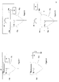
- FIGS. 7-13 illustrate different forms of receivers that provide the same mechanism of decoding of the encoded light 15 .
- the electrode 14 a corresponds to the electrode 14 in FIG. 1 , except that the shape is flatter.
- FIG. 7 illustrates the broader principle that the shape, size and characteristics of all of the electrodes shown can be modified from the ones described and shown herein and still accomplish the intended decoding.
- FIG. 8 two additional alternative design principles are embodied.
- the order of encounter of the electrodes can be altered; namely the “straight path” electrode 30 for the OFF condition can appear to the electron beam 13 after passing the “altered path” electrode 14 b / 24 a for the ON condition.
- the electrodes 14 b and 24 a can be separate electrodes electrically connected to the detector 16 , or they can be one doughnut-shaped electrode with the hole in the center providing the path for the electron beam 13 to pass when it is not be diverted.
- FIG. 8 also illustrates the alternative principle that the detector 16 need not detect the current difference between the ON and OFF electrodes, but can instead detect change in current in the ON electrode(s). In that instance, the OFF electrode (in the case of FIG. 8 the electrode 30 ) takes the electron beam to ground (or may capture it with a Faraday cup and employ it for power requirements of the electric circuits).
- FIG. 9 illustrates a detector in which the detector 16 detects current conditions on the OFF electrode 14 c and compares it to ground. It could alternatively do the same for the ON electrode (instead or in addition to the OFF electrode).
- FIG. 10 illustrates the ON electrodes 14 b / 24 a taking the electron beam to ground and the OFF electrode 30 providing the detector 16 with a signal referenced to ground whenever the electron beam follows the non-deflected path 13 b.
- FIG. 11 illustrates basically side-by-side electrodes 24 and 14 b .
- electrode 14 b slightly extends into the straight-line path 13 b so the OFF condition is detected by it.
- Electrode 24 is positioned to capture the electron beam when it is deflected to the 13 a path in the ON condition.
- FIG. 12 we illustrate detectors that provide improved sensitivity and noise-reduction by referencing the received electron beam to the cathode.
- FIG. 12 the principle of the detector referenced to an electric characteristic of the cathode is shown.
- the example embodiment shows the OFF electrode 14 a receiving the OFF path 13 b and the ON electrode 24 receiving the ON paths 13 a and 13 c .
- the detector receives the beam and references it to an electrical characteristic that it receives from the cathode (or another element associated with the electron beam source).
- the OFF electrode can be grounded, Faraday cupped, etc.
- the ON electrode 24 is electrically coupled to the detector 16 .
- a current detector 28 that measures the current between the cathode 20 and anode 19 . In operation, when the electron beam is deflected to the electrode 24 , the current in that electrode 24 is detected by the detector 16 (and then diverted ground, a Faraday cup, etc.) and referenced to the current detected by detector 28 such that noise in the electron beam source can be cancelled, improving detection sensitivity.
- the shield 29 a / 29 b in FIGS. 13 and 14 illustrate an example option that can reduce the strays. Specifically, it is advantageous to keep stray electrons out of the area where the electron beam 13 (either deflected or non-deflected) will be traveling to avoid collisions between the stray electrons and the electrons in the beam 13 .
- the shields 29 a and 29 b are grounded and sit in front of (relative to the beam path) the detector being employed in order to provide the stray electrons another “to-ground” attraction before they enter the area where the electron beam 13 is traveling.
- the shields 29 a and 29 b can be employed with any type of detector (for example, any of FIGS. 7-12 ).
- FIGS. 16 and 17 describe an optional electrode structure that will also better capture the electrons in the electron beam 13 , thereby reducing the possibility of stray electrons returning “up-stream” and interfering with the electron beam 13 .
- the electrode 60 (which can be any of the electrode embodiments earlier described) is in the structural form of a baffle such that approaching electrons in the beam 13 have a multiple chance of being absorbed.
- the OFF electrode 60 is shown with the baffles, but the ON detector electrode 61 can also (or instead) be baffled.
- the baffles are more particularly shown in FIG.
- FIG. 15 illustrates an AM (amplitude demodulation) detector based on the above-described detector principles.
- the cathode, anode, and resonant structures of, for example FIG. 1 are combined into the box “Charge Source and Resonant Structures” but basically operate according to the principles outlined in FIG. 1 .
- the encoded light 15 contains data from the data source 18 that is modulated with more than two binary conditions.
- the encoded light invokes the electric field in the resonant structures in accordance with a characteristic of the light (for example, intensity, frequency, polarity, etc.) such that the electric field in the resonant structures bears an amplitude relation to the light characteristic.
- the data from the data source 18 can then be encoded by the light characteristic such that greater than two data states—and indeed within the limits of practicality, infinite data states can be amplitude modulated on the data source.
- the resonant structures encountering that light 15 respond by electric field amplitude changes in accordance with the light characteristic.
- the electron beam 13 passing close to the resonant structures couple that amplitude characteristic and deflect at an angle commensurate with the amplitude modulation.
- high amplitude modulation can result in the beam diversion to path 46 and onto electrodes 32 / 37 , where it is detected by detector portion 45 .
- Lesser amplitudes result in beam path diversions to paths 47 , 48 , and 49 , respectively encountering electrodes 33 / 38 , 34 / 39 and 35 / 40 and detector portions 44 , 43 , and 42 .
- No diversion i.e., a “0” amplitude state
- “analog” differences in light characteristic can be detected by amplitude demodulation.
- the sensitivity of the data can be adjusted based on the number and size of the electrodes 32 - 40 . By adding more electrodes, a greater number of differentiated amplitude increments can be detected and thus greater data volume can be encoded;
- FIG. 19 illustrates a graph of percent reflectivity (Y-axis) versus wavelength of light measured in nm (X-axis).
- Y-axis percent reflectivity
- X-axis wavelength of light measured in nm
- the dominant “dips” in the graph illustrate wavelengths of the light that were absorbed well by one or more of the resonant structures at the polarity shown. Other light frequencies and finger lengths could be mapped and used as alternatives.
- the graph is significant to show that the resonant structures are in fact absorbing the encoded light energy.
- the graph is also significant in illustrating the effect of polarization angle on the absorption. In essence, the graph illustrates that absorption occurs and that it is enhanced when polarization of the light is parallel to the finger length.
- the graphs for polarization angles 0 and 180 show large absorption at the dips and for angles 90 and 270, for example show lower absorption.
- Light intensity of the encoded light 15 affects electric field strength produced in the resonant structures 12 and thus can be used to angularly modulate the beam path. So too can changes in polarization and light frequency, such that they too can be used to encode the data on the light 15 to produce a corresponding path alteration in the electron beam 13 at the receiver 10 .
- a heterodyne receiver can be built such that an input signal representing a modulated EMR signal is received by a mixer 2000 .
- the mixer 2000 also receives a signal from a local oscillator 2020 .
- the mixer 2000 combines the input signal and the signal from the local oscillator 2020 to produce two beat frequencies representing the sum and the difference of the two signals.
- the difference of the two signals is the signal of interest and termed the “intermediate frequency” or IF.
- the IF represents the signal that was added to the carrier wave on the transmitter side.
- the IF may be applied to an intermediate frequency filter 2030 and/or an IF amplifier 2040 .
- the resulting signal is then applied to a demodulator 2050 to produce the demodulated signal.
- a heterodyne receiver 2150 that operates up to optical frequencies can be constructed, e.g., as shown in FIG. 21 .
- ultra-small resonant structures 12 respond to a modulated EMR signal 15 , as described above.
- the ultra-small resonant structures 12 (collectively referenced as 2125 , e.g., in FIG. 22 a ) resonate at the beat frequencies which are the sum and the difference of the modulated EMR signal 15 and the local EMR 2100 from the local oscillator 2020 .
- the intermediate frequency corresponding to the difference of the modulated EMR signal 15 and the local EMR 2100 from the local oscillator 2020 can be determined.
- the intermediate frequency optionally can then be filtered and/or amplified, either using actual circuitry or via digital signal processing.
- the intermediate frequency or the amplified/filtered intermediate frequency can then be applied to a demodulator to obtain the signal that was modulated on the carrier wave at the transmitter.
- the heterodyne receiver 2150 of FIG. 21 is modified to be a heterodyne receiver 2250 including plural local oscillators 2020 a - 2020 c such that the local EMR 2100 can be selected to be one of a number of frequencies, depending on the how the receiver is tuned.
- a multi-frequency receiver as shown in FIGS. 22 a - 22 c
- 22 a - 22 c can first receive a signal modulated on a first carrier frequency by using oscillator 2020 a as the local oscillator (and blocking the outputs of local oscillators 2020 b and 2020 c ) while orienting or deflecting the charged particle beam (e.g., using deflectors 2275 ) toward a resonant structure 2125 a with dimensions selected to receive the first carrier frequency.
- oscillator 2020 b can be used as the local oscillator while orienting or deflecting the charged particle beam (e.g., using deflectors 2275 ) toward a resonant structure 2125 b with dimensions selected to receive the second carrier frequency. Receipt of a signal carried on the third carrier signal works analogously using resonant structure 2125 c.
- a heterodyne receiver 2350 can be constructed by replacing the plural local oscillators 2020 a - 2020 c of FIGS. 22 a - 22 c with a variable oscillator 2300 .
- the variable oscillator 2300 can be dynamically tuned to the frequency corresponding to the carrier frequency of the signal that is desired to be demodulated.
- Intel Corporation of California manufactures a tunable laser system which can be used as the variable oscillator by providing applying (e.g., via an optical interconnection such as fiber optic cable) the output of the laser to the resonant structure acting as a mixer.
- variable oscillator 2300 can instead be a series of other resonant structures which are excited by one or more charged particle beams. Which one of the series of resonant structures is selected may depend on an input to the variable oscillator 2300 where the input controls a deflector which varies an amount of deflection of the charged particle beam. Additional details of such a set of selectable resonant structures and their deflector can be found in co-pending U.S. application Ser. No. 11/410,924, described in greater detail above.
- Such resonant structures may each include at least one corresponding filter to filter out frequencies other than the desired predominant frequency corresponding to the selected resonant structure.
- the deflector selects a first resonant structure to act as the oscillating frequency, that resonant structure may produce relatively small amounts of other, non-predominant frequencies.
- a filter filters out the relatively small amounts of other, non-predominant frequencies.
- any one of the heterodyne receivers 2150 / 2250 / 2350 described above can be repeated within an array of receivers such that a signal to be received can be spatially resolved. Such a spatial resolution may be useful in applications such as image capture.
- the receivers may share a local oscillator which applies its output to each of the receivers 2150 / 2250 / 2350 , or the array may include one local oscillator per receiver 2150 / 2250 / 2350 .
- a subset (e.g., half) of the receivers 2150 / 2250 / 2350 may share one local oscillator with at least one other subset sharing at least one other local receiver.
- any one of the heterodyne receivers 2150 / 2250 / 2350 described above can be repeated within a matrix of receivers such that a signal to be received can be spatially resolved.
- a matrix is still an array of receivers, but it is a two-dimensional array rather than a one-dimensional array.
- the receivers may share a local oscillator which applies its output to each of the receivers 2150 / 2250 / 2350 , or the matrix may include one local oscillator per receiver 2150 / 2250 / 2350 .
- a subset (e.g., half) of the receivers 2150 / 2250 / 2350 may share one local oscillator with at least one other subset sharing at least one other local receiver.
- each row or each column of the matrix may share a local oscillator.
- the matrix of FIG. 25 can be switched to receive each of the frequencies in succession.
- the receivers 2150 / 2250 / 2350 may first be controlled to receive a red signal, then switched to receive a green signal, then switched to receive a blue signal, where the red, green and blue images are combined to form an RGB image.
- the heterodyne receivers 2150 / 2250 / 2350 described above can be repeated within a matrix of receivers such that a multi-frequency signal to be received can be spatially resolved simultaneously.
- a subset of the receivers 2150 / 2250 / 2350 may be dynamically dedicated to receive at a particular frequency that is different from its neighbor. For example, every third receiver 2150 / 2250 / 2350 R may be switched to be dedicated to receiving a red signal, while a different group of every third receiver 2150 / 2250 / 2350 G is switched to be dedicated to receiving a green signal, and the last group of every third receiver 2150 / 2250 / 2350 B is switched to be dedicated to receiving a blue signal.
- red, green and blue signals can be received simultaneously.
- other signals may also be received simultaneously with those signals.
- Such other signals may include any other signals that can be received by the ultra-small resonant structures described herein.
- Such signals may include infra-red or other terahertz signals which can be used in conjunction with or in place of visible imaging (e.g., when visible imaging is degraded or impossible due to environmental conditions).
- a configuration such as FIG. 25 could be augmented with an additional resonant structure such that the whole array could receive the non-visible signals.
- additional optical devices such as lens and deflectors may be required to focus the image onto an array or matrix of receivers. It is further possible to include an array or matrix of lens for use with the array or matrix of receivers such that a series of images with varying focal distances can be received in parallel by the array or matrix.
Abstract
Description
-
- 1. U.S. patent application Ser. No. 11/238,991, entitled “Ultra-Small Resonating Charged Particle Beam Modulator,” filed Sep. 30, 2005;
- 2. U.S. patent application Ser. No. 10/917,511, entitled “Patterning Thin Metal Film by Dry Reactive Ion Etching,” filed on Aug. 13, 2004;
- 3. U.S. application Ser. No. 11/203,407, entitled “Method Of Patterning Ultra-Small Structures,” filed on Aug. 15, 2005;
- 4. U.S. application Ser. No. 11/243,476, entitled “Structures And Methods For Coupling Energy From An Electromagnetic Wave,” filed on Oct. 5, 2005;
- 5. U.S. application Ser. No. 11/243,477, entitled “Electron beam induced resonance,” filed on Oct. 5, 2005;
- 6. U.S. application Ser. No. 11/325,448, entitled “Selectable Frequency Light Emitter from Single Metal Layer,” filed Jan. 5, 2006;
- 7. U.S. application Ser. No. 11/325,432, entitled, “Matrix Array Display,” filed Jan. 5, 2006;
- 8. U.S. application Ser. No. 11/302,471, entitled “Coupled Nano-Resonating Energy Emitting Structures,” filed Dec. 14, 2005;
- 9. U.S. application Ser. No. 11/325,571, entitled “Switching Micro-resonant Structures by Modulating a Beam of Charged Particles,” filed Jan. 5, 2006;
- 10. U.S. application Ser. No. 11/325,534, entitled “Switching Microresonant Structures Using at Least One Director,” filed Jan. 5, 2006;
- 11. U.S. application Ser. No. 11/350,812, entitled “Conductive Polymers for Electroplating,” filed Feb. 10, 2006;
- 12. U.S. application Ser. No. 11/349,963, entitled “Method and Structure for Coupling Two Microcircuits,” filed Feb. 9, 2006;
- 13. U.S. application Ser. No. 11/353,208, entitled “Electron Beam Induced Resonance,” filed Feb. 14, 2006;
- 14. U.S. application Ser. No. 11/400,280, entitled “Resonant Detectors for Optical Signals,” filed Apr. 10, 2006;
- 15. U.S. application Ser. No. 11/410,924, entitled “Selectable Frequency EMR Emitter,” filed Apr. 26, 2006;
- 16. U.S. application Ser. No. 11/411,129, entitled “Micro Free Electron Laser (FEL),” filed Apr. 26, 2006; and
- 17. U.S. application Ser. No. 11/418,088, entitled “Heterodyne Receiver Using Resonant Structures,” filed herewith.
Claims (21)
Priority Applications (4)
| Application Number | Priority Date | Filing Date | Title |
|---|---|---|---|
| US11/418,118 US7342441B2 (en) | 2006-05-05 | 2006-05-05 | Heterodyne receiver array using resonant structures |
| EP06773729A EP2022166A1 (en) | 2006-05-05 | 2006-06-22 | Heterodyne receiver array using resonant structures |
| PCT/US2006/024218 WO2007130102A1 (en) | 2006-05-05 | 2006-06-22 | Heterodyne receiver array using resonant structures |
| TW095126190A TW200743131A (en) | 2006-05-05 | 2006-07-18 | Heterodyne receiver array using resonant structures |
Applications Claiming Priority (1)
| Application Number | Priority Date | Filing Date | Title |
|---|---|---|---|
| US11/418,118 US7342441B2 (en) | 2006-05-05 | 2006-05-05 | Heterodyne receiver array using resonant structures |
Publications (2)
| Publication Number | Publication Date |
|---|---|
| US20070259641A1 US20070259641A1 (en) | 2007-11-08 |
| US7342441B2 true US7342441B2 (en) | 2008-03-11 |
Family
ID=38661776
Family Applications (1)
| Application Number | Title | Priority Date | Filing Date |
|---|---|---|---|
| US11/418,118 Expired - Fee Related US7342441B2 (en) | 2006-05-05 | 2006-05-05 | Heterodyne receiver array using resonant structures |
Country Status (4)
| Country | Link |
|---|---|
| US (1) | US7342441B2 (en) |
| EP (1) | EP2022166A1 (en) |
| TW (1) | TW200743131A (en) |
| WO (1) | WO2007130102A1 (en) |
Cited By (45)
| Publication number | Priority date | Publication date | Assignee | Title |
|---|---|---|---|---|
| US20060216940A1 (en) * | 2004-08-13 | 2006-09-28 | Virgin Islands Microsystems, Inc. | Methods of producing structures for electron beam induced resonance using plating and/or etching |
| US20060289761A1 (en) * | 2004-12-15 | 2006-12-28 | Bahram Nabet | Nanowire based plasmonics |
| US20070034518A1 (en) * | 2005-08-15 | 2007-02-15 | Virgin Islands Microsystems, Inc. | Method of patterning ultra-small structures |
| US20070075263A1 (en) * | 2005-09-30 | 2007-04-05 | Virgin Islands Microsystems, Inc. | Ultra-small resonating charged particle beam modulator |
| US20070152938A1 (en) * | 2006-01-05 | 2007-07-05 | Virgin Islands Microsystems, Inc. | Resonant structure-based display |
| US20070154846A1 (en) * | 2006-01-05 | 2007-07-05 | Virgin Islands Microsystems, Inc. | Switching micro-resonant structures using at least one director |
| US20070152176A1 (en) * | 2006-01-05 | 2007-07-05 | Virgin Islands Microsystems, Inc. | Selectable frequency light emitter |
| US20070190794A1 (en) * | 2006-02-10 | 2007-08-16 | Virgin Islands Microsystems, Inc. | Conductive polymers for the electroplating |
| US20070200063A1 (en) * | 2006-02-28 | 2007-08-30 | Virgin Islands Microsystems, Inc. | Wafer-level testing of light-emitting resonant structures |
| US20070200770A1 (en) * | 2006-02-28 | 2007-08-30 | Virgin Islands Microsystems, Inc. | Integrated filter in antenna-based detector |
| US20070200910A1 (en) * | 2006-02-28 | 2007-08-30 | Virgin Islands Microsystems, Inc. | Electro-photographic devices incorporating ultra-small resonant structures |
| US20070235651A1 (en) * | 2006-04-10 | 2007-10-11 | Virgin Island Microsystems, Inc. | Resonant detector for optical signals |
| US20070252089A1 (en) * | 2006-04-26 | 2007-11-01 | Virgin Islands Microsystems, Inc. | Charged particle acceleration apparatus and method |
| US20070259465A1 (en) * | 2006-05-05 | 2007-11-08 | Virgin Islands Microsystems, Inc. | Integration of vacuum microelectronic device with integrated circuit |
| US20070257206A1 (en) * | 2006-05-05 | 2007-11-08 | Virgin Islands Microsystems, Inc. | Transmission of data between microchips using a particle beam |
| US20070257622A1 (en) * | 2006-05-05 | 2007-11-08 | Virgin Islands Microsystems, Inc. | Coupling energy in a plasmon wave to an electron beam |
| US20070257273A1 (en) * | 2006-05-05 | 2007-11-08 | Virgin Island Microsystems, Inc. | Novel optical cover for optical chip |
| US20070257749A1 (en) * | 2006-05-05 | 2007-11-08 | Virgin Islands Microsystems, Inc. | Coupling a signal through a window |
| US20070257619A1 (en) * | 2006-05-05 | 2007-11-08 | Virgin Islands Microsystems, Inc. | Selectable frequency light emitter |
| US20070257328A1 (en) * | 2006-05-05 | 2007-11-08 | Virgin Islands Microsystems, Inc. | Detecting plasmons using a metallurgical junction |
| US20070257199A1 (en) * | 2006-05-05 | 2007-11-08 | Virgin Islands Microsystems, Inc. | Heterodyne receiver using resonant structures |
| US20070259488A1 (en) * | 2006-05-05 | 2007-11-08 | Virgin Islands Microsystems, Inc. | Single layer construction for ultra small devices |
| US20070258720A1 (en) * | 2006-05-05 | 2007-11-08 | Virgin Islands Microsystems, Inc. | Inter-chip optical communication |
| US20070258126A1 (en) * | 2006-05-05 | 2007-11-08 | Virgin Islands Microsystems, Inc. | Electro-optical switching system and method |
| US20070257739A1 (en) * | 2006-05-05 | 2007-11-08 | Virgin Islands Microsystems, Inc. | Local plane array incorporating ultra-small resonant structures |
| US20070264030A1 (en) * | 2006-04-26 | 2007-11-15 | Virgin Islands Microsystems, Inc. | Selectable frequency EMR emitter |
| US20070262234A1 (en) * | 2006-05-05 | 2007-11-15 | Virgin Islands Microsystems, Inc. | Stray charged particle removal device |
| US20070264023A1 (en) * | 2006-04-26 | 2007-11-15 | Virgin Islands Microsystems, Inc. | Free space interchip communications |
| US20070274365A1 (en) * | 2006-05-26 | 2007-11-29 | Virgin Islands Microsystems, Inc. | Periodically complex resonant structures |
| US20070272931A1 (en) * | 2006-05-05 | 2007-11-29 | Virgin Islands Microsystems, Inc. | Methods, devices and systems producing illumination and effects |
| US20070272876A1 (en) * | 2006-05-26 | 2007-11-29 | Virgin Islands Microsystems, Inc. | Receiver array using shared electron beam |
| US20080001098A1 (en) * | 2006-06-28 | 2008-01-03 | Virgin Islands Microsystems, Inc. | Data on light bulb |
| US20080067941A1 (en) * | 2006-05-05 | 2008-03-20 | Virgin Islands Microsystems, Inc. | Shielding of integrated circuit package with high-permeability magnetic material |
| US20080067940A1 (en) * | 2006-05-05 | 2008-03-20 | Virgin Islands Microsystems, Inc. | Surface plasmon signal transmission |
| US20080073590A1 (en) * | 2006-09-22 | 2008-03-27 | Virgin Islands Microsystems, Inc. | Free electron oscillator |
| US20080083881A1 (en) * | 2006-05-15 | 2008-04-10 | Virgin Islands Microsystems, Inc. | Plasmon wave propagation devices and methods |
| US20080149828A1 (en) * | 2006-12-20 | 2008-06-26 | Virgin Islands Microsystems, Inc. | Low terahertz source and detector |
| US20080296517A1 (en) * | 2005-12-14 | 2008-12-04 | Virgin Islands Microsystems, Inc. | Coupling light of light emitting resonator to waveguide |
| US20090072698A1 (en) * | 2007-06-19 | 2009-03-19 | Virgin Islands Microsystems, Inc. | Microwave coupled excitation of solid state resonant arrays |
| US20090290604A1 (en) * | 2006-04-26 | 2009-11-26 | Virgin Islands Microsystems, Inc. | Micro free electron laser (FEL) |
| US7656094B2 (en) | 2006-05-05 | 2010-02-02 | Virgin Islands Microsystems, Inc. | Electron accelerator for ultra-small resonant structures |
| US7723698B2 (en) | 2006-05-05 | 2010-05-25 | Virgin Islands Microsystems, Inc. | Top metal layer shield for ultra-small resonant structures |
| US7728397B2 (en) | 2006-05-05 | 2010-06-01 | Virgin Islands Microsystems, Inc. | Coupled nano-resonating energy emitting structures |
| US7791053B2 (en) | 2007-10-10 | 2010-09-07 | Virgin Islands Microsystems, Inc. | Depressed anode with plasmon-enabled devices such as ultra-small resonant structures |
| US20100252514A1 (en) * | 2009-04-03 | 2010-10-07 | Min-Ju Chung | Foldable baseball equipment rack |
Families Citing this family (8)
| Publication number | Priority date | Publication date | Assignee | Title |
|---|---|---|---|---|
| EP2223486A4 (en) * | 2007-11-12 | 2012-03-14 | Kaonetics Technologies Inc | Method and apparatus for enhancing signal carrier performance in wireless networks |
| US8200151B2 (en) * | 2007-11-12 | 2012-06-12 | Kaonetics Technologies, Inc. | Method and apparatus for enhancing signal carrier performance in wireless networks |
| US20090123163A1 (en) * | 2007-11-12 | 2009-05-14 | James Cornwell | Method of producing a highly permeable stable rf wavefront suitable as a data carrier |
| US7839145B2 (en) * | 2007-11-16 | 2010-11-23 | Prosis, Llc | Directed-energy imaging system |
| US8476901B2 (en) | 2007-11-13 | 2013-07-02 | Kaonetics Technologies, Inc. | Directed-energy systems and methods for disrupting electronic circuits |
| WO2009064488A1 (en) * | 2007-11-14 | 2009-05-22 | James Cornwell | Wireless identification system using a directed-energy device as a tag reader |
| KR101912163B1 (en) * | 2012-02-27 | 2018-10-26 | 삼성전자주식회사 | Method of modulation and demodulation for nano communication,and receiver device using the method |
| US9852871B1 (en) * | 2016-06-03 | 2017-12-26 | Tsinghua University | Detecting system based on terahertz wave |
Citations (92)
| Publication number | Priority date | Publication date | Assignee | Title |
|---|---|---|---|---|
| US1948384A (en) | 1932-01-26 | 1934-02-20 | Research Corp | Method and apparatus for the acceleration of ions |
| US2307086A (en) | 1941-05-07 | 1943-01-05 | Univ Leland Stanford Junior | High frequency electrical apparatus |
| US2431396A (en) | 1942-12-21 | 1947-11-25 | Rca Corp | Current magnitude-ratio responsive amplifier |
| US2473477A (en) | 1946-07-24 | 1949-06-14 | Raythcon Mfg Company | Magnetic induction device |
| US2634372A (en) | 1953-04-07 | Super high-frequency electromag | ||
| US2932798A (en) | 1956-01-05 | 1960-04-12 | Research Corp | Imparting energy to charged particles |
| US3571642A (en) | 1968-01-17 | 1971-03-23 | Ca Atomic Energy Ltd | Method and apparatus for interleaved charged particle acceleration |
| US3761828A (en) | 1970-12-10 | 1973-09-25 | J Pollard | Linear particle accelerator with coast through shield |
| US3923568A (en) | 1974-01-14 | 1975-12-02 | Int Plasma Corp | Dry plasma process for etching noble metal |
| US3989347A (en) | 1974-06-20 | 1976-11-02 | Siemens Aktiengesellschaft | Acousto-optical data input transducer with optical data storage and process for operation thereof |
| US4282436A (en) | 1980-06-04 | 1981-08-04 | The United States Of America As Represented By The Secretary Of The Navy | Intense ion beam generation with an inverse reflex tetrode (IRT) |
| US4482779A (en) | 1983-04-19 | 1984-11-13 | The United States Of America As Represented By The Administrator Of National Aeronautics And Space Administration | Inelastic tunnel diodes |
| US4727550A (en) | 1985-09-19 | 1988-02-23 | Chang David B | Radiation source |
| US4740973A (en) | 1984-05-21 | 1988-04-26 | Madey John M J | Free electron laser |
| US4746201A (en) | 1967-03-06 | 1988-05-24 | Gordon Gould | Polarizing apparatus employing an optical element inclined at brewster's angle |
| US4829527A (en) | 1984-04-23 | 1989-05-09 | The United States Of America As Represented By The Secretary Of The Army | Wideband electronic frequency tuning for orotrons |
| US4838021A (en) | 1987-12-11 | 1989-06-13 | Hughes Aircraft Company | Electrostatic ion thruster with improved thrust modulation |
| US5023563A (en) | 1989-06-08 | 1991-06-11 | Hughes Aircraft Company | Upshifted free electron laser amplifier |
| US5157000A (en) | 1989-07-10 | 1992-10-20 | Texas Instruments Incorporated | Method for dry etching openings in integrated circuit layers |
| US5163118A (en) | 1986-11-10 | 1992-11-10 | The United States Of America As Represented By The Secretary Of The Air Force | Lattice mismatched hetrostructure optical waveguide |
| US5185073A (en) | 1988-06-21 | 1993-02-09 | International Business Machines Corporation | Method of fabricating nendritic materials |
| US5199918A (en) | 1991-11-07 | 1993-04-06 | Microelectronics And Computer Technology Corporation | Method of forming field emitter device with diamond emission tips |
| US5263043A (en) | 1990-08-31 | 1993-11-16 | Trustees Of Dartmouth College | Free electron laser utilizing grating coupling |
| US5262656A (en) | 1991-06-07 | 1993-11-16 | Thomson-Csf | Optical semiconductor transceiver with chemically resistant layers |
| US5268788A (en) | 1991-06-25 | 1993-12-07 | Smiths Industries Public Limited Company | Display filter arrangements |
| US5268693A (en) | 1990-08-31 | 1993-12-07 | Trustees Of Dartmouth College | Semiconductor film free electron laser |
| US5302240A (en) | 1991-01-22 | 1994-04-12 | Kabushiki Kaisha Toshiba | Method of manufacturing semiconductor device |
| US5446814A (en) | 1993-11-05 | 1995-08-29 | Motorola | Molded reflective optical waveguide |
| US5608263A (en) | 1994-09-06 | 1997-03-04 | The Regents Of The University Of Michigan | Micromachined self packaged circuits for high-frequency applications |
| US5668368A (en) | 1992-02-21 | 1997-09-16 | Hitachi, Ltd. | Apparatus for suppressing electrification of sample in charged beam irradiation apparatus |
| US5705443A (en) | 1995-05-30 | 1998-01-06 | Advanced Technology Materials, Inc. | Etching method for refractory materials |
| US5737458A (en) | 1993-03-29 | 1998-04-07 | Martin Marietta Corporation | Optical light pipe and microwave waveguide interconnects in multichip modules formed using adaptive lithography |
| US5744919A (en) | 1996-12-12 | 1998-04-28 | Mishin; Andrey V. | CW particle accelerator with low particle injection velocity |
| US5757009A (en) | 1996-12-27 | 1998-05-26 | Northrop Grumman Corporation | Charged particle beam expander |
| US5767013A (en) | 1996-08-26 | 1998-06-16 | Lg Semicon Co., Ltd. | Method for forming interconnection in semiconductor pattern device |
| US5790585A (en) | 1996-11-12 | 1998-08-04 | The Trustees Of Dartmouth College | Grating coupling free electron laser apparatus and method |
| US5811943A (en) | 1996-09-23 | 1998-09-22 | Schonberg Research Corporation | Hollow-beam microwave linear accelerator |
| US5821836A (en) | 1997-05-23 | 1998-10-13 | The Regents Of The University Of Michigan | Miniaturized filter assembly |
| US5821902A (en) | 1993-09-02 | 1998-10-13 | Inmarsat | Folded dipole microstrip antenna |
| US5831270A (en) | 1996-02-19 | 1998-11-03 | Nikon Corporation | Magnetic deflectors and charged-particle-beam lithography systems incorporating same |
| US5847745A (en) | 1995-03-03 | 1998-12-08 | Futaba Denshi Kogyo K.K. | Optical write element |
| US5889449A (en) | 1995-12-07 | 1999-03-30 | Space Systems/Loral, Inc. | Electromagnetic transmission line elements having a boundary between materials of high and low dielectric constants |
| US5902489A (en) | 1995-11-08 | 1999-05-11 | Hitachi, Ltd. | Particle handling method by acoustic radiation force and apparatus therefore |
| US6008496A (en) | 1997-05-05 | 1999-12-28 | University Of Florida | High resolution resonance ionization imaging detector and method |
| US6040625A (en) | 1997-09-25 | 2000-03-21 | I/O Sensors, Inc. | Sensor package arrangement |
| US6060833A (en) | 1996-10-18 | 2000-05-09 | Velazco; Jose E. | Continuous rotating-wave electron beam accelerator |
| US6080529A (en) | 1997-12-12 | 2000-06-27 | Applied Materials, Inc. | Method of etching patterned layers useful as masking during subsequent etching or for damascene structures |
| US6195199B1 (en) | 1997-10-27 | 2001-02-27 | Kanazawa University | Electron tube type unidirectional optical amplifier |
| US6222866B1 (en) | 1997-01-06 | 2001-04-24 | Fuji Xerox Co., Ltd. | Surface emitting semiconductor laser, its producing method and surface emitting semiconductor laser array |
| US6297511B1 (en) | 1999-04-01 | 2001-10-02 | Raytheon Company | High frequency infrared emitter |
| US20010025925A1 (en) | 2000-03-28 | 2001-10-04 | Kabushiki Kaisha Toshiba | Charged particle beam system and pattern slant observing method |
| US6338968B1 (en) | 1998-02-02 | 2002-01-15 | Signature Bioscience, Inc. | Method and apparatus for detecting molecular binding events |
| US6370306B1 (en) | 1997-12-15 | 2002-04-09 | Seiko Instruments Inc. | Optical waveguide probe and its manufacturing method |
| US6373194B1 (en) | 2000-06-01 | 2002-04-16 | Raytheon Company | Optical magnetron for high efficiency production of optical radiation |
| US20020053638A1 (en) | 1998-07-03 | 2002-05-09 | Dieter Winkler | Apparatus and method for examing specimen with a charged particle beam |
| US6407516B1 (en) | 2000-05-26 | 2002-06-18 | Exaconnect Inc. | Free space electron switch |
| US6441298B1 (en) | 2000-08-15 | 2002-08-27 | Nec Research Institute, Inc | Surface-plasmon enhanced photovoltaic device |
| US20020135665A1 (en) | 2001-03-20 | 2002-09-26 | Keith Gardner | Led print head for electrophotographic printer |
| US20030012925A1 (en) | 2001-07-16 | 2003-01-16 | Motorola, Inc. | Process for fabricating semiconductor structures and devices utilizing the formation of a compliant substrate for materials used to form the same and including an etch stop layer used for back side processing |
| US20030016421A1 (en) | 2000-06-01 | 2003-01-23 | Small James G. | Wireless communication system with high efficiency/high power optical source |
| US20030016412A1 (en) | 2001-07-17 | 2003-01-23 | Alcatel | Monitoring unit for optical burst mode signals |
| US20030034535A1 (en) | 2001-08-15 | 2003-02-20 | Motorola, Inc. | Mems devices suitable for integration with chip having integrated silicon and compound semiconductor devices, and methods for fabricating such devices |
| US6545425B2 (en) | 2000-05-26 | 2003-04-08 | Exaconnect Corp. | Use of a free space electron switch in a telecommunications network |
| US6577040B2 (en) | 1999-01-14 | 2003-06-10 | The Regents Of The University Of Michigan | Method and apparatus for generating a signal having at least one desired output frequency utilizing a bank of vibrating micromechanical devices |
| US6603915B2 (en) | 2001-02-05 | 2003-08-05 | Fujitsu Limited | Interposer and method for producing a light-guiding structure |
| US20030155521A1 (en) | 2000-02-01 | 2003-08-21 | Hans-Peter Feuerbaum | Optical column for charged particle beam device |
| US20030164947A1 (en) | 2000-04-18 | 2003-09-04 | Matthias Vaupel | Spr sensor |
| US6624916B1 (en) | 1997-02-11 | 2003-09-23 | Quantumbeam Limited | Signalling system |
| US20030179974A1 (en) | 2002-03-20 | 2003-09-25 | Estes Michael J. | Surface plasmon devices |
| US6636653B2 (en) | 2001-02-02 | 2003-10-21 | Teravicta Technologies, Inc. | Integrated optical micro-electromechanical systems and methods of fabricating and operating the same |
| US6642907B2 (en) | 2001-01-12 | 2003-11-04 | The Furukawa Electric Co., Ltd. | Antenna device |
| US20030206708A1 (en) | 2002-03-20 | 2003-11-06 | Estes Michael J. | Surface plasmon devices |
| US20040061053A1 (en) | 2001-02-28 | 2004-04-01 | Yoshifumi Taniguchi | Method and apparatus for measuring physical properties of micro region |
| US6738176B2 (en) | 2002-04-30 | 2004-05-18 | Mario Rabinowitz | Dynamic multi-wavelength switching ensemble |
| US6741781B2 (en) | 2000-09-29 | 2004-05-25 | Kabushiki Kaisha Toshiba | Optical interconnection circuit board and manufacturing method thereof |
| US20040108473A1 (en) | 2000-06-09 | 2004-06-10 | Melnychuk Stephan T. | Extreme ultraviolet light source |
| US6782205B2 (en) | 2001-06-25 | 2004-08-24 | Silicon Light Machines | Method and apparatus for dynamic equalization in wavelength division multiplexing |
| US6791438B2 (en) | 2001-10-30 | 2004-09-14 | Matsushita Electric Industrial Co., Ltd. | Radio frequency module and method for manufacturing the same |
| US6829286B1 (en) | 2000-05-26 | 2004-12-07 | Opticomp Corporation | Resonant cavity enhanced VCSEL/waveguide grating coupler |
| US6834152B2 (en) | 2001-09-10 | 2004-12-21 | California Institute Of Technology | Strip loaded waveguide with low-index transition layer |
| US6870438B1 (en) | 1999-11-10 | 2005-03-22 | Kyocera Corporation | Multi-layered wiring board for slot coupling a transmission line to a waveguide |
| US6885262B2 (en) | 2002-11-05 | 2005-04-26 | Ube Industries, Ltd. | Band-pass filter using film bulk acoustic resonator |
| US6909104B1 (en) | 1999-05-25 | 2005-06-21 | Nawotec Gmbh | Miniaturized terahertz radiation source |
| US6909092B2 (en) | 2002-05-16 | 2005-06-21 | Ebara Corporation | Electron beam apparatus and device manufacturing method using same |
| US6944369B2 (en) | 2001-05-17 | 2005-09-13 | Sioptical, Inc. | Optical coupler having evanescent coupling region |
| US6953291B2 (en) | 2003-06-30 | 2005-10-11 | Finisar Corporation | Compact package design for vertical cavity surface emitting laser array to optical fiber cable connection |
| US6965625B2 (en) | 2000-09-22 | 2005-11-15 | Vermont Photonics, Inc. | Apparatuses and methods for generating coherent electromagnetic laser radiation |
| US6995406B2 (en) | 2002-06-10 | 2006-02-07 | Tsuyoshi Tojo | Multibeam semiconductor laser, semiconductor light-emitting device and semiconductor device |
| US7092588B2 (en) | 2002-11-20 | 2006-08-15 | Seiko Epson Corporation | Optical interconnection circuit between chips, electrooptical device and electronic equipment |
| US7092603B2 (en) | 2004-03-03 | 2006-08-15 | Fujitsu Limited | Optical bridge for chip-to-board interconnection and methods of fabrication |
| US20060216940A1 (en) * | 2004-08-13 | 2006-09-28 | Virgin Islands Microsystems, Inc. | Methods of producing structures for electron beam induced resonance using plating and/or etching |
| US7122978B2 (en) | 2004-04-19 | 2006-10-17 | Mitsubishi Denki Kabushiki Kaisha | Charged-particle beam accelerator, particle beam radiation therapy system using the charged-particle beam accelerator, and method of operating the particle beam radiation therapy system |
Family Cites Families (23)
| Publication number | Priority date | Publication date | Assignee | Title |
|---|---|---|---|---|
| US7064500B2 (en) * | 2000-05-26 | 2006-06-20 | Exaconnect Corp. | Semi-conductor interconnect using free space electron switch |
| US6635949B2 (en) * | 2002-01-04 | 2003-10-21 | Intersil Americas Inc. | Symmetric inducting device for an integrated circuit having a ground shield |
| US6841795B2 (en) * | 2002-10-25 | 2005-01-11 | The University Of Connecticut | Semiconductor devices employing at least one modulation doped quantum well structure and one or more etch stop layers for accurate contact formation |
| CN100533589C (en) * | 2002-11-26 | 2009-08-26 | 株式会社东芝 | Magnetic unit and memory |
| JP4249474B2 (en) * | 2002-12-06 | 2009-04-02 | セイコーエプソン株式会社 | Wavelength multiplexing chip-to-chip optical interconnection circuit |
| JP2004191392A (en) * | 2002-12-06 | 2004-07-08 | Seiko Epson Corp | Wavelength multiple intra-chip optical interconnection circuit, electro-optical device and electronic appliance |
| US20040159900A1 (en) * | 2003-01-27 | 2004-08-19 | 3M Innovative Properties Company | Phosphor based light sources having front illumination |
| JP4044453B2 (en) * | 2003-02-06 | 2008-02-06 | 株式会社東芝 | Quantum memory and information processing method using quantum memory |
| US20040171272A1 (en) * | 2003-02-28 | 2004-09-02 | Applied Materials, Inc. | Method of etching metallic materials to form a tapered profile |
| US6954515B2 (en) * | 2003-04-25 | 2005-10-11 | Varian Medical Systems, Inc., | Radiation sources and radiation scanning systems with improved uniformity of radiation intensity |
| WO2004101857A2 (en) * | 2003-05-07 | 2004-11-25 | Microfabrica Inc. | Methods and apparatus for forming multi-layer structures using adhered masks |
| US6884335B2 (en) * | 2003-05-20 | 2005-04-26 | Novellus Systems, Inc. | Electroplating using DC current interruption and variable rotation rate |
| US20050194258A1 (en) * | 2003-06-27 | 2005-09-08 | Microfabrica Inc. | Electrochemical fabrication methods incorporating dielectric materials and/or using dielectric substrates |
| US20050067286A1 (en) * | 2003-09-26 | 2005-03-31 | The University Of Cincinnati | Microfabricated structures and processes for manufacturing same |
| JP4370945B2 (en) * | 2004-03-11 | 2009-11-25 | ソニー株式会社 | Measuring method of dielectric constant |
| US6996303B2 (en) * | 2004-03-12 | 2006-02-07 | Fujitsu Limited | Flexible optical waveguides for backplane optical interconnections |
| US7454095B2 (en) * | 2004-04-27 | 2008-11-18 | California Institute Of Technology | Integrated plasmon and dielectric waveguides |
| US20060062258A1 (en) * | 2004-07-02 | 2006-03-23 | Vanderbilt University | Smith-Purcell free electron laser and method of operating same |
| US20060035173A1 (en) * | 2004-08-13 | 2006-02-16 | Mark Davidson | Patterning thin metal films by dry reactive ion etching |
| KR100623477B1 (en) * | 2004-08-25 | 2006-09-19 | 한국정보통신대학교 산학협력단 | Optical printed circuit boards and optical interconnection blocks using optical fiber bundles |
| US7466326B2 (en) * | 2005-01-21 | 2008-12-16 | Konica Minolta Business Technologies, Inc. | Image forming method and image forming apparatus |
| JP4945561B2 (en) * | 2005-06-30 | 2012-06-06 | デ,ロシェモント,エル.,ピエール | Electrical component and method of manufacturing the same |
| US20070013765A1 (en) * | 2005-07-18 | 2007-01-18 | Eastman Kodak Company | Flexible organic laser printer |
-
2006
- 2006-05-05 US US11/418,118 patent/US7342441B2/en not_active Expired - Fee Related
- 2006-06-22 WO PCT/US2006/024218 patent/WO2007130102A1/en active Application Filing
- 2006-06-22 EP EP06773729A patent/EP2022166A1/en not_active Withdrawn
- 2006-07-18 TW TW095126190A patent/TW200743131A/en unknown
Patent Citations (100)
| Publication number | Priority date | Publication date | Assignee | Title |
|---|---|---|---|---|
| US2634372A (en) | 1953-04-07 | Super high-frequency electromag | ||
| US1948384A (en) | 1932-01-26 | 1934-02-20 | Research Corp | Method and apparatus for the acceleration of ions |
| US2307086A (en) | 1941-05-07 | 1943-01-05 | Univ Leland Stanford Junior | High frequency electrical apparatus |
| US2431396A (en) | 1942-12-21 | 1947-11-25 | Rca Corp | Current magnitude-ratio responsive amplifier |
| US2473477A (en) | 1946-07-24 | 1949-06-14 | Raythcon Mfg Company | Magnetic induction device |
| US2932798A (en) | 1956-01-05 | 1960-04-12 | Research Corp | Imparting energy to charged particles |
| US4746201A (en) | 1967-03-06 | 1988-05-24 | Gordon Gould | Polarizing apparatus employing an optical element inclined at brewster's angle |
| US3571642A (en) | 1968-01-17 | 1971-03-23 | Ca Atomic Energy Ltd | Method and apparatus for interleaved charged particle acceleration |
| US3761828A (en) | 1970-12-10 | 1973-09-25 | J Pollard | Linear particle accelerator with coast through shield |
| US3923568A (en) | 1974-01-14 | 1975-12-02 | Int Plasma Corp | Dry plasma process for etching noble metal |
| US3989347A (en) | 1974-06-20 | 1976-11-02 | Siemens Aktiengesellschaft | Acousto-optical data input transducer with optical data storage and process for operation thereof |
| US4282436A (en) | 1980-06-04 | 1981-08-04 | The United States Of America As Represented By The Secretary Of The Navy | Intense ion beam generation with an inverse reflex tetrode (IRT) |
| US4482779A (en) | 1983-04-19 | 1984-11-13 | The United States Of America As Represented By The Administrator Of National Aeronautics And Space Administration | Inelastic tunnel diodes |
| US4829527A (en) | 1984-04-23 | 1989-05-09 | The United States Of America As Represented By The Secretary Of The Army | Wideband electronic frequency tuning for orotrons |
| US4740973A (en) | 1984-05-21 | 1988-04-26 | Madey John M J | Free electron laser |
| US4727550A (en) | 1985-09-19 | 1988-02-23 | Chang David B | Radiation source |
| US5163118A (en) | 1986-11-10 | 1992-11-10 | The United States Of America As Represented By The Secretary Of The Air Force | Lattice mismatched hetrostructure optical waveguide |
| US5354709A (en) | 1986-11-10 | 1994-10-11 | The United States Of America As Represented By The Secretary Of The Air Force | Method of making a lattice mismatched heterostructure optical waveguide |
| US4838021A (en) | 1987-12-11 | 1989-06-13 | Hughes Aircraft Company | Electrostatic ion thruster with improved thrust modulation |
| US5185073A (en) | 1988-06-21 | 1993-02-09 | International Business Machines Corporation | Method of fabricating nendritic materials |
| US5023563A (en) | 1989-06-08 | 1991-06-11 | Hughes Aircraft Company | Upshifted free electron laser amplifier |
| US5157000A (en) | 1989-07-10 | 1992-10-20 | Texas Instruments Incorporated | Method for dry etching openings in integrated circuit layers |
| US5263043A (en) | 1990-08-31 | 1993-11-16 | Trustees Of Dartmouth College | Free electron laser utilizing grating coupling |
| US5268693A (en) | 1990-08-31 | 1993-12-07 | Trustees Of Dartmouth College | Semiconductor film free electron laser |
| US5302240A (en) | 1991-01-22 | 1994-04-12 | Kabushiki Kaisha Toshiba | Method of manufacturing semiconductor device |
| US5262656A (en) | 1991-06-07 | 1993-11-16 | Thomson-Csf | Optical semiconductor transceiver with chemically resistant layers |
| US5268788A (en) | 1991-06-25 | 1993-12-07 | Smiths Industries Public Limited Company | Display filter arrangements |
| US5199918A (en) | 1991-11-07 | 1993-04-06 | Microelectronics And Computer Technology Corporation | Method of forming field emitter device with diamond emission tips |
| US5668368A (en) | 1992-02-21 | 1997-09-16 | Hitachi, Ltd. | Apparatus for suppressing electrification of sample in charged beam irradiation apparatus |
| US5737458A (en) | 1993-03-29 | 1998-04-07 | Martin Marietta Corporation | Optical light pipe and microwave waveguide interconnects in multichip modules formed using adaptive lithography |
| US5821902A (en) | 1993-09-02 | 1998-10-13 | Inmarsat | Folded dipole microstrip antenna |
| US5446814A (en) | 1993-11-05 | 1995-08-29 | Motorola | Molded reflective optical waveguide |
| US5608263A (en) | 1994-09-06 | 1997-03-04 | The Regents Of The University Of Michigan | Micromachined self packaged circuits for high-frequency applications |
| US5847745A (en) | 1995-03-03 | 1998-12-08 | Futaba Denshi Kogyo K.K. | Optical write element |
| US5705443A (en) | 1995-05-30 | 1998-01-06 | Advanced Technology Materials, Inc. | Etching method for refractory materials |
| US5902489A (en) | 1995-11-08 | 1999-05-11 | Hitachi, Ltd. | Particle handling method by acoustic radiation force and apparatus therefore |
| US20020027481A1 (en) | 1995-12-07 | 2002-03-07 | Fiedziuszko Slawomir J. | Electromagnetic transmission line elements having a boundary between materials of high and low dielectric constants |
| US5889449A (en) | 1995-12-07 | 1999-03-30 | Space Systems/Loral, Inc. | Electromagnetic transmission line elements having a boundary between materials of high and low dielectric constants |
| US6281769B1 (en) | 1995-12-07 | 2001-08-28 | Space Systems/Loral Inc. | Electromagnetic transmission line elements having a boundary between materials of high and low dielectric constants |
| US5831270A (en) | 1996-02-19 | 1998-11-03 | Nikon Corporation | Magnetic deflectors and charged-particle-beam lithography systems incorporating same |
| US5767013A (en) | 1996-08-26 | 1998-06-16 | Lg Semicon Co., Ltd. | Method for forming interconnection in semiconductor pattern device |
| US5811943A (en) | 1996-09-23 | 1998-09-22 | Schonberg Research Corporation | Hollow-beam microwave linear accelerator |
| US6060833A (en) | 1996-10-18 | 2000-05-09 | Velazco; Jose E. | Continuous rotating-wave electron beam accelerator |
| US5790585A (en) | 1996-11-12 | 1998-08-04 | The Trustees Of Dartmouth College | Grating coupling free electron laser apparatus and method |
| US5744919A (en) | 1996-12-12 | 1998-04-28 | Mishin; Andrey V. | CW particle accelerator with low particle injection velocity |
| US5757009A (en) | 1996-12-27 | 1998-05-26 | Northrop Grumman Corporation | Charged particle beam expander |
| US6222866B1 (en) | 1997-01-06 | 2001-04-24 | Fuji Xerox Co., Ltd. | Surface emitting semiconductor laser, its producing method and surface emitting semiconductor laser array |
| US6624916B1 (en) | 1997-02-11 | 2003-09-23 | Quantumbeam Limited | Signalling system |
| US6008496A (en) | 1997-05-05 | 1999-12-28 | University Of Florida | High resolution resonance ionization imaging detector and method |
| US5821836A (en) | 1997-05-23 | 1998-10-13 | The Regents Of The University Of Michigan | Miniaturized filter assembly |
| US6040625A (en) | 1997-09-25 | 2000-03-21 | I/O Sensors, Inc. | Sensor package arrangement |
| US6195199B1 (en) | 1997-10-27 | 2001-02-27 | Kanazawa University | Electron tube type unidirectional optical amplifier |
| US6080529A (en) | 1997-12-12 | 2000-06-27 | Applied Materials, Inc. | Method of etching patterned layers useful as masking during subsequent etching or for damascene structures |
| US6370306B1 (en) | 1997-12-15 | 2002-04-09 | Seiko Instruments Inc. | Optical waveguide probe and its manufacturing method |
| US6376258B2 (en) | 1998-02-02 | 2002-04-23 | Signature Bioscience, Inc. | Resonant bio-assay device and test system for detecting molecular binding events |
| US6338968B1 (en) | 1998-02-02 | 2002-01-15 | Signature Bioscience, Inc. | Method and apparatus for detecting molecular binding events |
| US20020009723A1 (en) | 1998-02-02 | 2002-01-24 | John Hefti | Resonant bio-assay device and test system for detecting molecular binding events |
| US20020053638A1 (en) | 1998-07-03 | 2002-05-09 | Dieter Winkler | Apparatus and method for examing specimen with a charged particle beam |
| US6577040B2 (en) | 1999-01-14 | 2003-06-10 | The Regents Of The University Of Michigan | Method and apparatus for generating a signal having at least one desired output frequency utilizing a bank of vibrating micromechanical devices |
| US6297511B1 (en) | 1999-04-01 | 2001-10-02 | Raytheon Company | High frequency infrared emitter |
| US6909104B1 (en) | 1999-05-25 | 2005-06-21 | Nawotec Gmbh | Miniaturized terahertz radiation source |
| US6870438B1 (en) | 1999-11-10 | 2005-03-22 | Kyocera Corporation | Multi-layered wiring board for slot coupling a transmission line to a waveguide |
| US20030155521A1 (en) | 2000-02-01 | 2003-08-21 | Hans-Peter Feuerbaum | Optical column for charged particle beam device |
| US20010025925A1 (en) | 2000-03-28 | 2001-10-04 | Kabushiki Kaisha Toshiba | Charged particle beam system and pattern slant observing method |
| US20030164947A1 (en) | 2000-04-18 | 2003-09-04 | Matthias Vaupel | Spr sensor |
| US6407516B1 (en) | 2000-05-26 | 2002-06-18 | Exaconnect Inc. | Free space electron switch |
| US6545425B2 (en) | 2000-05-26 | 2003-04-08 | Exaconnect Corp. | Use of a free space electron switch in a telecommunications network |
| US6829286B1 (en) | 2000-05-26 | 2004-12-07 | Opticomp Corporation | Resonant cavity enhanced VCSEL/waveguide grating coupler |
| US6504303B2 (en) | 2000-06-01 | 2003-01-07 | Raytheon Company | Optical magnetron for high efficiency production of optical radiation, and 1/2λ induced pi-mode operation |
| US20030016421A1 (en) | 2000-06-01 | 2003-01-23 | Small James G. | Wireless communication system with high efficiency/high power optical source |
| US6373194B1 (en) | 2000-06-01 | 2002-04-16 | Raytheon Company | Optical magnetron for high efficiency production of optical radiation |
| US20040108473A1 (en) | 2000-06-09 | 2004-06-10 | Melnychuk Stephan T. | Extreme ultraviolet light source |
| US6441298B1 (en) | 2000-08-15 | 2002-08-27 | Nec Research Institute, Inc | Surface-plasmon enhanced photovoltaic device |
| US6965625B2 (en) | 2000-09-22 | 2005-11-15 | Vermont Photonics, Inc. | Apparatuses and methods for generating coherent electromagnetic laser radiation |
| US6741781B2 (en) | 2000-09-29 | 2004-05-25 | Kabushiki Kaisha Toshiba | Optical interconnection circuit board and manufacturing method thereof |
| US6642907B2 (en) | 2001-01-12 | 2003-11-04 | The Furukawa Electric Co., Ltd. | Antenna device |
| US6636653B2 (en) | 2001-02-02 | 2003-10-21 | Teravicta Technologies, Inc. | Integrated optical micro-electromechanical systems and methods of fabricating and operating the same |
| US6603915B2 (en) | 2001-02-05 | 2003-08-05 | Fujitsu Limited | Interposer and method for producing a light-guiding structure |
| US20040061053A1 (en) | 2001-02-28 | 2004-04-01 | Yoshifumi Taniguchi | Method and apparatus for measuring physical properties of micro region |
| US20020135665A1 (en) | 2001-03-20 | 2002-09-26 | Keith Gardner | Led print head for electrophotographic printer |
| US6944369B2 (en) | 2001-05-17 | 2005-09-13 | Sioptical, Inc. | Optical coupler having evanescent coupling region |
| US6782205B2 (en) | 2001-06-25 | 2004-08-24 | Silicon Light Machines | Method and apparatus for dynamic equalization in wavelength division multiplexing |
| US20030012925A1 (en) | 2001-07-16 | 2003-01-16 | Motorola, Inc. | Process for fabricating semiconductor structures and devices utilizing the formation of a compliant substrate for materials used to form the same and including an etch stop layer used for back side processing |
| US20030016412A1 (en) | 2001-07-17 | 2003-01-23 | Alcatel | Monitoring unit for optical burst mode signals |
| US20030034535A1 (en) | 2001-08-15 | 2003-02-20 | Motorola, Inc. | Mems devices suitable for integration with chip having integrated silicon and compound semiconductor devices, and methods for fabricating such devices |
| US6834152B2 (en) | 2001-09-10 | 2004-12-21 | California Institute Of Technology | Strip loaded waveguide with low-index transition layer |
| US6791438B2 (en) | 2001-10-30 | 2004-09-14 | Matsushita Electric Industrial Co., Ltd. | Radio frequency module and method for manufacturing the same |
| US20030206708A1 (en) | 2002-03-20 | 2003-11-06 | Estes Michael J. | Surface plasmon devices |
| US20030179974A1 (en) | 2002-03-20 | 2003-09-25 | Estes Michael J. | Surface plasmon devices |
| US7010183B2 (en) | 2002-03-20 | 2006-03-07 | The Regents Of The University Of Colorado | Surface plasmon devices |
| US7177515B2 (en) | 2002-03-20 | 2007-02-13 | The Regents Of The University Of Colorado | Surface plasmon devices |
| US6738176B2 (en) | 2002-04-30 | 2004-05-18 | Mario Rabinowitz | Dynamic multi-wavelength switching ensemble |
| US6909092B2 (en) | 2002-05-16 | 2005-06-21 | Ebara Corporation | Electron beam apparatus and device manufacturing method using same |
| US6995406B2 (en) | 2002-06-10 | 2006-02-07 | Tsuyoshi Tojo | Multibeam semiconductor laser, semiconductor light-emitting device and semiconductor device |
| US6885262B2 (en) | 2002-11-05 | 2005-04-26 | Ube Industries, Ltd. | Band-pass filter using film bulk acoustic resonator |
| US7092588B2 (en) | 2002-11-20 | 2006-08-15 | Seiko Epson Corporation | Optical interconnection circuit between chips, electrooptical device and electronic equipment |
| US6953291B2 (en) | 2003-06-30 | 2005-10-11 | Finisar Corporation | Compact package design for vertical cavity surface emitting laser array to optical fiber cable connection |
| US7092603B2 (en) | 2004-03-03 | 2006-08-15 | Fujitsu Limited | Optical bridge for chip-to-board interconnection and methods of fabrication |
| US7122978B2 (en) | 2004-04-19 | 2006-10-17 | Mitsubishi Denki Kabushiki Kaisha | Charged-particle beam accelerator, particle beam radiation therapy system using the charged-particle beam accelerator, and method of operating the particle beam radiation therapy system |
| US20060216940A1 (en) * | 2004-08-13 | 2006-09-28 | Virgin Islands Microsystems, Inc. | Methods of producing structures for electron beam induced resonance using plating and/or etching |
Non-Patent Citations (96)
| Title |
|---|
| "Antenna Arrays." May 18, 2002. www.tpub.com/content/neets/14183/css/14183<SUB>-</SUB>159.htm. |
| "Array of Nanoklystrons for Frequency Agility or Redundancy," NASA's Jet Propulsion Laboratory, NASA Tech Briefs, NPO-21033. 2001. |
| "Diffraction Grating," hyperphysics.phy-astr.gsu.edu/hbase/phyopt/grating.html. |
| "Hardware Development Programs," Calabazas Creek Research, Inc. found at http://calcreek.com/hardware.html. |
| Alford, T.L. et al., "Advanced silver-based metallization patterning for ULSI applications," Microelectronic Engineering 55, 2001, pp. 383-388, Elsevier Science B.V. |
| Amato, Ivan, "An Everyman's Free-Electron Laser?" Science, New Series, Oct. 16, 1992, p. 401, vol. 258 No. 5081, American Association for the Advancement of Science. |
| Andrews, H.L. et al., "Dispersion and Attenuation in a Smith-Purcell Free Electron Laser," The American Physical Society, Physical Review Special Topics-Accelerators and Beams 8 (2005), pp. 050703-1-050703-9. |
| Backe, H. et al. "Investigation of Far-Infrared Smith-Purcell Radiation at the 3.41 MeV Electron Injector Linac of the Mainz Microtron MAMI," Institut fur Kernphysik, Universitat Mainz, D-55099, Mainz Germany. |
| Bakhtyari, A. et al., "Horn Resonator Boosts Miniature Free-Electron Laser Power," Applied Physics Letters, May 12, 2003, pp. 3150-3152, vol. 82, No. 19, American Institute of Physics. |
| Bakhtyari, Dr. Arash, "Gain Mechanism in a Smith-Purcell MicroFEL," Abstract, Department of Physics and Astronomy, Dartmouth College. |
| Bhattacharjee, Sudeep et al., "Folded Waveguide Traveling-Wave Tube Sources for Terahertz Radiation." IEEE Transactions on Plasma Science, vol. 32. No. 3, Jun. 2004, pp. 1002-1014. |
| Booske, J.H. et al., "Microfabricated TWTs as High Power, Wideband Sources of THz Radiation". |
| Brau, C.A. et al., "Gain and Coherent Radiation from a Smith-Purcell Free Electron Laser," Proceedings of the 2004 FEL Conference, pp. 278-281. |
| Brownell, J.H. et al., "Improved muFEL Performance with Novel Resonator," Jan. 7, 2005, from website: www.frascati.enea.it/thz-bridge/workshop/presentations/Wednesday/We-07-Brownell.ppt. |
| Brownell, J.H. et al., "The Angular Distribution of the Power Produced by Smith-Purcell Radiation," J. Phys. D: Appl. Phys. 1997, pp. 2478-2481, vol. 30, IOP Publishing Ltd., United Kingdom. |
| Chuang, S.L. et al., "Enhancement of Smith-Purcell Radiation from a Grating with Surface-Plasmon Excitation," Journal of the Optical Society of America, Jun. 1984, pp. 672-676, vol. 1 No. 6, Optical Society of America. |
| Chuang, S.L. et al., "Smith-Purcell Radiation from a Charge Moving Above a Penetrable Grating," IEEE MTT-S Digest, 1983, pp. 405-406, IEEE. |
| Far-IR, Sub-MM & MM Detector Technology Workshop list of manuscripts, session 6 2002. |
| Feltz, W.F. et al., "Near-Continuous Profiling of Temperature, Moisture, and Atmospheric Stability Using the Atmospheric Emitted Radiance Interferometer (AERI)," Journal of Applied Meteorology, May 2003, vol. 42 No. 5, H.W. Wilson Company, pp. 584-597. |
| Freund, H.P. et al., "Linearized Field Theory of a Smith-Purcell Traveling Wave Tube," IEEE Transactions on Plasma Science, Jun. 2004, pp. 1015-1027, vol. 32 No. 3, IEEE. |
| Gallerano, G.P. et al., "Overview of Terahertz Radiation Sources," Proceedings of the 2004 FEL Conference, pp. 216-221. |
| Goldstein, M. et al., "Demonstration of a Micro Far-Infrared Smith-Purcell Emitter," Applied Physics Letters, Jul. 28, 1997, pp. 452-454, vol. 71 No. 4, American Institute of Physics. |
| Gover, A. et al., "Angular Radiation Pattern of Smith-Purcell Radiation," Journal of the Optical Society of America, Oct. 1984, pp. 723-728, vol. 1 No. 5, Optical Society of America. |
| Grishin, Yu. A. et al., "Pulsed Orotron-A New Microwave Source for Submillimeter Pulse High-Field Electron Paramagnetic Resonance Spectroscopy," Review of Scientific Instruments, Sep. 2004, pp. 2926-2936, vol. 75 No. 9, American Institute of Physics. |
| International Search Report and Written Opinion mailed Nov. 23, 2007 in International Application No. PCT/US2006/022786. |
| Ishizuka, H. et al., "Smith-Purcell Experiment Utilizing a Field-Emitter Array Cathode: Measurements of Radiation," Nuclear Instruments and Methods in Physics Research, 2001, pp. 593-598, A 475, Elsevier Science B.V. |
| Ishizuka, H. et al., "Smith-Purcell Radiation Experiment Using a Field-Emission Array Cathode," Nuclear Instuments and Methods in Physics Research, 2000, pp. 276-280, A 445, Elsevier Science B.V. |
| Ives, Lawrence et al., "Development of Backward Wave Oscillators for Terahertz Applications," Terahertz for Military and Security Applications, Proceedings of SPIE vol. 5070 (2003), pp. 71-82. |
| Ives, R. Lawrence, "IVEC Summary, Session 2, Sources I" 2002. |
| Jonietz, Erika, "Nano Antenna Gold nanospheres show path to all-optical computing," Technology Review, Dec. 2005/Jan. 2006, p. 32. |
| Joo, Youngcheol et al., "Air Cooling of IC Chip with Novel Microchannels Monolithically Formed on Chip Front Surface," Cooling and Thermal Design of Electronic Systems (HTD-vol. 319 & EEP-vol. 15), International Mechanical Engineering Congress and Exposition, San Francisco, CA Nov. 1995 pp. 117-121. |
| Joo, Youngcheol et al., "Fabrication of Monolithic Microchannels for IC Chip Cooling," 1995, Mechanical, Aerospace and Nuclear Engineering Department, University of California at Los Angeles. |
| Jung, K.B. et al., "Patterning of Cu, Co, Fe, and Ag for magnetic nanostructures," J. Vac. Sci. Technol. A 15(3), May/Jun. 1997, pp. 1780-1784. |
| Kapp, Oscar H. et al., "Modification of a Scanning Electron Microscope to Produce Smith-Purcell Radiation," Review of Scientific Instruments, Nov. 2004, pp. 4732-4741, vol. 75 No. 11, American Institute of Physics. |
| Kiener, C. et al., "Investigation of the Mean Free Path of Hot Electrons in GaAs/AlGaAs Heterostructures," Semicond. Sci. Technol., 1994, pp. 193-197, vol. 9, IOP Publishing Ltd., United Kingdom. |
| Kim, Shang Hoon, "Quantum Mechanical Theory fo Free-Electron Two-Quantum Stark Emission Driven by Transverse Motion," Journal of the Physical Society of Japan, Aug. 1993, vol. 62 No. 8, pp. 2528-2532. |
| Korbly, S.E. et al., "Progress on a Smith-Purcell Radiation Bunch Length Diagnostic," Plasma Science and Fusion Center, MIT, Cambridge, MA. |
| Kormann, T. et al., "A Photoelectron Source for the Study of Smith-Purcell Radiation". |
| Kube, G. et al., "Observation of Optical Smith-Purcell Radiation at an Electron Beam Energy of 855 MeV," Physical Review E, May 8, 2002, vol. 65, The American Physical Society, pp. 056501-1-056501-15. |
| Lee Kwang-Cheol et al., "Deep X-Ray Mask with Integrated Actuator for 3D Microfabrication", Conference: Pacific Rim Workshop on Transducers and Micro/Nano Technologies, (Xiamen CHN), Jul. 22, 2002. |
| Liu, Chuan Sheng, et al., "Stimulated Coherent Smith-Purcell Radiation from a Metallic Grating," IEEE Journal of Quantum Electronics, Oct. 1999, pp. 1386-1389, vol. 35, No. 10, IEEE. |
| Manohara, Harish et al., "Field Emission Testing of Carbon Nanotubes for THz Frequency Vacuum Microtube Sources." Abstract. Dec. 2003. from SPIEWeb. |
| Manohara, Harish M. et al., "Design and Fabrication of a THz Nanoklystron" (www.sofia.usra.edu/det<SUB>-</SUB>workshop/ posters/session 3/3-43manohara<SUB>-</SUB>poster.pdf), PowerPoint Presentation. |
| Manohara, Harish M. et al., "Design and Fabrication of a THz Nanoklystron". |
| Markoff, John, "A Chip That Can Transfer Data Using Laser Light," The New York Times, Sep. 18, 2006. |
| McDaniel, James C. et al., "Smith-Purcell Radiation in the High Conductivity and Plasma Frequency Limits," Applied Optics, Nov. 15, 1989, pp. 4924-4929, vol. 28 No. 22, Optical Society of America. |
| Meyer, Stephan, "Far IR, Sum-MM & MM Detector Technology Workshop Summary," Oct. 2002. (may date the Manohara documents). |
| Mokhoff, Nicolas, "Optical-speed light detector promises fast space talk," EETimes Online, Mar. 20, 2006, from website: www.eetimes.com/showArticle.jhtml?articleID=183701047. |
| Nguyen, Phucanh et al., "Novel technique to pattern silver using CF4 and CF4/O2 glow discharges," J.Vac. Sci. Technol. B 19(1), Jan./Feb. 2001, American Vacuum Society, pp. 158-165. |
| Nguyen, Phucanh et al., "Reactive ion etch of patterned and blanket silver thin films in CI2/O2 and O2 glow discharges," J. Vac. Sci, Technol. B. 17 (5), Sep./Oct. 1999, American Vacuum Society, pp. 2204-2209. |
| Ohtaka, Kazuo, "Smith-Purcell Radiation from Metallic and Dielectric Photonic Crystals," Center for Frontier Science, pp. 272-273, Chiba University, 1-33 Yayoi, Inage-ku, Chiba-shi, Japan. |
| Phototonics Research, "Surface-Plasmon-Enhanced Random Laser Demonstrated," Phototonics Spectra, Feb. 2005, pp. 112-113. |
| Platt, C.L. et al., "A New Resonator Design for Smith-Purcell Free Electron Lasers," 6Q19, p. 296. |
| Potylitsin, A.P., "Resonant Diffraction Radiation and Smith-Purcell Effect," (Abstract), arXiv: physics/9803043 v2 Apr. 13, 1998. |
| Potylitsyn, A.P., "Resonant Diffraction Radiation and Smith-Purcell Effect," Physics Letters A, Feb. 2, 1998, pp. 112-116, A 238, Elsevier Science B.V. |
| S. Hoogland et al., "A solution-processed 1.53 mum quantum dot laser with temperature-invariant emission wavelength," Optics Express, vol. 14, No. 8, Apr. 17, 2006, pp. 3273-3281. |
| S.M. Sze, "Semiconductor Devices Physics and Technology", 2nd Edition, Chapters 9 and 12, Copyright 1985, 2002. |
| Savilov, Andrey V., "Stimulated Wave Scattering in the Smith-Purcell FEL," IEEE Transactions on Plasma Science, Oct. 2001, pp. 820-823, vol. 29 No. 5, IEEE. |
| Schachter, Levi et al., "Smith-Purcell Oscillator in an Exponential Gain Regime," Journal of Applied Physics, Apr. 15, 1989, pp. 3267-3269, vol. 65 No. 8, American Institute of Physics. |
| Schachter, Levi, "Influence of the Guiding Magnetic Field on the Performance of a Smith-Purcell Amplifier Operating in the Weak Compton Regime," Journal of the Optical Society of America, May 1990, pp. 873-876, vol. 7 No. 5, Optical Society of America. |
| Schachter, Levi, "The Influence of the Guided Magnetic Field on the Performance of a Smith-Purcell Amplifier Operating In the Strong Compton Regime," Journal of Applied Physics, Apr. 15, 1990, pp. 3582-3592, vol. 67 No. 8, American Institute of Physics. |
| Search Report and Written Opinion mailed Aug. 24, 2007 in PCT Appln. No. PCT/US2006/022768. |
| Search Report and Written Opinion mailed Aug. 31, 2007 in PCT Appln. No. PCT/US2006/022680. |
| Search Report and Written Opinion mailed Feb. 12, 2007 in PCT Appln. No. PCT/US2006/022682. |
| Search Report and Written Opinion mailed Feb. 20, 2007 in PCT Appln. No. PCT/US2006/022676. |
| Search Report and Written Opinion mailed Feb. 20, 2007 in PCT Appln. No. PCT/US2006/022772. |
| Search Report and Written Opinion mailed Feb. 20, 2007 in PCT Appln. No. PCT/US2006/022780. |
| Search Report and Written Opinion mailed Feb. 21, 2007 in PCT Appln. No. PCT/US2006/022684. |
| Search Report and Written Opinion mailed Jan. 17, 2007 in PCT Appln. No. PCT/US2006/022777. |
| Search Report and Written Opinion mailed Jan. 23, 2007 in PCT Appln. No. PCT/US2006/022781. |
| Search Report and Written Opinion mailed Jul. 16, 2007 in PCT Appln. No. PCT/US2006/022774. |
| Search Report and Written Opinion mailed Jul. 20, 2007 in PCT Appln. No. PCT/US2006/024216. |
| Search Report and Written Opinion mailed Jul. 26, 2007 in PCT Appln. No. PCT/US2006/022776. |
| Search Report and Written Opinion mailed Jun. 20, 2007 in PCT Appln. No. PCT/US2006/022779. |
| Search Report and Written Opinion mailed Mar. 7, 2007 in PCT Appln. No. PCT/US2006/022775. |
| Search Report and Written Opinion mailed Oct. 25, 2007 in PCT Appln. No. PCT/US2006/022687. |
| Search Report and Written Opinion mailed Oct. 26, 2007 in PCT Appln. No. PCT/US2006/022675. |
| Search Report and Written Opinion mailed Sep. 12, 2007 in PCT Appln. No. PCT/US2006/022767. |
| Search Report and Written Opinion mailed Sep. 13, 2007 in PCT Appln. No. PCT/US2006/024217. |
| Search Report and Written Opinion mailed Sep. 17, 2007 in PCT Appln. No. PCT/US2006/022689. |
| Search Report and Written Opinion mailed Sep. 17, 2007 in PCT Appln. No. PCT/US2006/022787. |
| Search Report and Written Opinion mailed Sep. 21, 2007 in PCT Appln. No. PCT/US2006/022688. |
| Search Report and Written Opinion mailed Sep. 25, 2007 in PCT appln. No. PCT/US2006/022681. |
| Search Report and Written Opinion mailed Sep. 26, 2007 in PCT Appln. No. PCT/US2006/024218. |
| Search Report and Written Opinion mailed Sep. 5, 2007 in PCT Appln. No. PCT/US2006/027428. |
| Shih, I. et al., "Experimental Investigations of Smith-Purcell Radiation," Journal of the Optical Society of America, Mar. 1990, pp. 351-356, vol. 7, No. 3, Optical Society of America. |
| Shih, I. et al., "Measurements of the Smith-Purcell Radiation," Journal of the Optical Society of America, Mar. 1990, pp. 345-350, vol. 7 No. 3, Optical Society of America. |
| Speller et al., "A Low-Noise MEMS Accelerometer for Unattended Ground Sensor Applications", Applied MEMS Inc., 12200 Parc Crest, Stafford, TX, USA 77477. |
| Swartz, J.C. et al., "THz-FIR Grating Coupled Radiation Source," Plasma Science, 1998. 1D02, p. 126. |
| Temkin, Richard, "Scanning with Ease Through the Far Infrared," Science, New Series, May 8, 1998, p. 854, vol. 280, No. 5365, American Association for the Advancement of Science. |
| Thurn-Albrecht et al., "Ultrahigh-Density Nanowire Arrays Grown in Self-Assembled Diblock Copolymer Templates", Science 290.5499, Dec. 15, 2000, pp. 2126-2129. |
| Walsh, J.E., et al., 1999. From website: http://www.ieee.org/organizations/pubs/newsletters/leos/feb99/hot2.htm. |
| Wentworth, Stuart M. et al., "Far-Infrared Composite Microbolometers," IEEE MTT-S Digest, 1990, pp. 1309-1310. |
| Yamamoto, N. et al., "Photon Emission From Silver Particles Induced by a High-Energy Electron Beam," Physical Review B, Nov. 6, 2001, pp. 205419-1-205419-9, vol. 64, the American Physical Society. |
| Yokoo, K. et al., "Smith-Purcell Radiation at Optical Wavelength Using a Field-Emitter Array," Technical Digest of IVMC, 2003, pp. 77-78. |
| Zeng, Yuxiao et al., "Processing and encapsulation of silver patterns by using reactive ion etch and ammonia anneal," Materials Chemistry and Physics 66, 2000, pp. 77-82. |
Cited By (71)
| Publication number | Priority date | Publication date | Assignee | Title |
|---|---|---|---|---|
| US7758739B2 (en) | 2004-08-13 | 2010-07-20 | Virgin Islands Microsystems, Inc. | Methods of producing structures for electron beam induced resonance using plating and/or etching |
| US20060216940A1 (en) * | 2004-08-13 | 2006-09-28 | Virgin Islands Microsystems, Inc. | Methods of producing structures for electron beam induced resonance using plating and/or etching |
| US20060289761A1 (en) * | 2004-12-15 | 2006-12-28 | Bahram Nabet | Nanowire based plasmonics |
| US8120014B2 (en) * | 2004-12-15 | 2012-02-21 | Drexel University | Nanowire based plasmonics |
| US20070034518A1 (en) * | 2005-08-15 | 2007-02-15 | Virgin Islands Microsystems, Inc. | Method of patterning ultra-small structures |
| US20070075263A1 (en) * | 2005-09-30 | 2007-04-05 | Virgin Islands Microsystems, Inc. | Ultra-small resonating charged particle beam modulator |
| US20070075907A1 (en) * | 2005-09-30 | 2007-04-05 | Virgin Islands Microsystems, Inc. | Electron beam induced resonance |
| US7714513B2 (en) | 2005-09-30 | 2010-05-11 | Virgin Islands Microsystems, Inc. | Electron beam induced resonance |
| US20070075264A1 (en) * | 2005-09-30 | 2007-04-05 | Virgin Islands Microsystems, Inc. | Electron beam induced resonance |
| US7791291B2 (en) | 2005-09-30 | 2010-09-07 | Virgin Islands Microsystems, Inc. | Diamond field emission tip and a method of formation |
| US7791290B2 (en) | 2005-09-30 | 2010-09-07 | Virgin Islands Microsystems, Inc. | Ultra-small resonating charged particle beam modulator |
| US20070075326A1 (en) * | 2005-09-30 | 2007-04-05 | Virgin Islands Microsystems, Inc. | Diamond field emmission tip and a method of formation |
| US20080296517A1 (en) * | 2005-12-14 | 2008-12-04 | Virgin Islands Microsystems, Inc. | Coupling light of light emitting resonator to waveguide |
| US20070152938A1 (en) * | 2006-01-05 | 2007-07-05 | Virgin Islands Microsystems, Inc. | Resonant structure-based display |
| US20090140178A1 (en) * | 2006-01-05 | 2009-06-04 | Virgin Islands Microsystems, Inc. | Switching micro-resonant structures by modulating a beam of charged particles |
| US8384042B2 (en) | 2006-01-05 | 2013-02-26 | Advanced Plasmonics, Inc. | Switching micro-resonant structures by modulating a beam of charged particles |
| US20070154846A1 (en) * | 2006-01-05 | 2007-07-05 | Virgin Islands Microsystems, Inc. | Switching micro-resonant structures using at least one director |
| US20070152176A1 (en) * | 2006-01-05 | 2007-07-05 | Virgin Islands Microsystems, Inc. | Selectable frequency light emitter |
| US20070190794A1 (en) * | 2006-02-10 | 2007-08-16 | Virgin Islands Microsystems, Inc. | Conductive polymers for the electroplating |
| US20070200770A1 (en) * | 2006-02-28 | 2007-08-30 | Virgin Islands Microsystems, Inc. | Integrated filter in antenna-based detector |
| US20070200063A1 (en) * | 2006-02-28 | 2007-08-30 | Virgin Islands Microsystems, Inc. | Wafer-level testing of light-emitting resonant structures |
| US20070200910A1 (en) * | 2006-02-28 | 2007-08-30 | Virgin Islands Microsystems, Inc. | Electro-photographic devices incorporating ultra-small resonant structures |
| US7688274B2 (en) | 2006-02-28 | 2010-03-30 | Virgin Islands Microsystems, Inc. | Integrated filter in antenna-based detector |
| US20070235651A1 (en) * | 2006-04-10 | 2007-10-11 | Virgin Island Microsystems, Inc. | Resonant detector for optical signals |
| US7876793B2 (en) | 2006-04-26 | 2011-01-25 | Virgin Islands Microsystems, Inc. | Micro free electron laser (FEL) |
| US7646991B2 (en) | 2006-04-26 | 2010-01-12 | Virgin Island Microsystems, Inc. | Selectable frequency EMR emitter |
| US20090290604A1 (en) * | 2006-04-26 | 2009-11-26 | Virgin Islands Microsystems, Inc. | Micro free electron laser (FEL) |
| US20070252089A1 (en) * | 2006-04-26 | 2007-11-01 | Virgin Islands Microsystems, Inc. | Charged particle acceleration apparatus and method |
| US20070264030A1 (en) * | 2006-04-26 | 2007-11-15 | Virgin Islands Microsystems, Inc. | Selectable frequency EMR emitter |
| US20070264023A1 (en) * | 2006-04-26 | 2007-11-15 | Virgin Islands Microsystems, Inc. | Free space interchip communications |
| US20070257206A1 (en) * | 2006-05-05 | 2007-11-08 | Virgin Islands Microsystems, Inc. | Transmission of data between microchips using a particle beam |
| US20070257619A1 (en) * | 2006-05-05 | 2007-11-08 | Virgin Islands Microsystems, Inc. | Selectable frequency light emitter |
| US20070272931A1 (en) * | 2006-05-05 | 2007-11-29 | Virgin Islands Microsystems, Inc. | Methods, devices and systems producing illumination and effects |
| US20070259465A1 (en) * | 2006-05-05 | 2007-11-08 | Virgin Islands Microsystems, Inc. | Integration of vacuum microelectronic device with integrated circuit |
| US8188431B2 (en) | 2006-05-05 | 2012-05-29 | Jonathan Gorrell | Integration of vacuum microelectronic device with integrated circuit |
| US20080067941A1 (en) * | 2006-05-05 | 2008-03-20 | Virgin Islands Microsystems, Inc. | Shielding of integrated circuit package with high-permeability magnetic material |
| US20080067940A1 (en) * | 2006-05-05 | 2008-03-20 | Virgin Islands Microsystems, Inc. | Surface plasmon signal transmission |
| US20070257622A1 (en) * | 2006-05-05 | 2007-11-08 | Virgin Islands Microsystems, Inc. | Coupling energy in a plasmon wave to an electron beam |
| US7986113B2 (en) | 2006-05-05 | 2011-07-26 | Virgin Islands Microsystems, Inc. | Selectable frequency light emitter |
| US20070257273A1 (en) * | 2006-05-05 | 2007-11-08 | Virgin Island Microsystems, Inc. | Novel optical cover for optical chip |
| US20070262234A1 (en) * | 2006-05-05 | 2007-11-15 | Virgin Islands Microsystems, Inc. | Stray charged particle removal device |
| US20070257749A1 (en) * | 2006-05-05 | 2007-11-08 | Virgin Islands Microsystems, Inc. | Coupling a signal through a window |
| US20070257739A1 (en) * | 2006-05-05 | 2007-11-08 | Virgin Islands Microsystems, Inc. | Local plane array incorporating ultra-small resonant structures |
| US7557647B2 (en) * | 2006-05-05 | 2009-07-07 | Virgin Islands Microsystems, Inc. | Heterodyne receiver using resonant structures |
| US20070258126A1 (en) * | 2006-05-05 | 2007-11-08 | Virgin Islands Microsystems, Inc. | Electro-optical switching system and method |
| US20070258720A1 (en) * | 2006-05-05 | 2007-11-08 | Virgin Islands Microsystems, Inc. | Inter-chip optical communication |
| US20070257328A1 (en) * | 2006-05-05 | 2007-11-08 | Virgin Islands Microsystems, Inc. | Detecting plasmons using a metallurgical junction |
| US7656094B2 (en) | 2006-05-05 | 2010-02-02 | Virgin Islands Microsystems, Inc. | Electron accelerator for ultra-small resonant structures |
| US7746532B2 (en) | 2006-05-05 | 2010-06-29 | Virgin Island Microsystems, Inc. | Electro-optical switching system and method |
| US7741934B2 (en) | 2006-05-05 | 2010-06-22 | Virgin Islands Microsystems, Inc. | Coupling a signal through a window |
| US20070259488A1 (en) * | 2006-05-05 | 2007-11-08 | Virgin Islands Microsystems, Inc. | Single layer construction for ultra small devices |
| US7710040B2 (en) | 2006-05-05 | 2010-05-04 | Virgin Islands Microsystems, Inc. | Single layer construction for ultra small devices |
| US20070257199A1 (en) * | 2006-05-05 | 2007-11-08 | Virgin Islands Microsystems, Inc. | Heterodyne receiver using resonant structures |
| US7718977B2 (en) | 2006-05-05 | 2010-05-18 | Virgin Island Microsystems, Inc. | Stray charged particle removal device |
| US7723698B2 (en) | 2006-05-05 | 2010-05-25 | Virgin Islands Microsystems, Inc. | Top metal layer shield for ultra-small resonant structures |
| US7728702B2 (en) | 2006-05-05 | 2010-06-01 | Virgin Islands Microsystems, Inc. | Shielding of integrated circuit package with high-permeability magnetic material |
| US7728397B2 (en) | 2006-05-05 | 2010-06-01 | Virgin Islands Microsystems, Inc. | Coupled nano-resonating energy emitting structures |
| US7732786B2 (en) | 2006-05-05 | 2010-06-08 | Virgin Islands Microsystems, Inc. | Coupling energy in a plasmon wave to an electron beam |
| US20080083881A1 (en) * | 2006-05-15 | 2008-04-10 | Virgin Islands Microsystems, Inc. | Plasmon wave propagation devices and methods |
| US7679067B2 (en) | 2006-05-26 | 2010-03-16 | Virgin Island Microsystems, Inc. | Receiver array using shared electron beam |
| US20070274365A1 (en) * | 2006-05-26 | 2007-11-29 | Virgin Islands Microsystems, Inc. | Periodically complex resonant structures |
| US20070272876A1 (en) * | 2006-05-26 | 2007-11-29 | Virgin Islands Microsystems, Inc. | Receiver array using shared electron beam |
| US7655934B2 (en) | 2006-06-28 | 2010-02-02 | Virgin Island Microsystems, Inc. | Data on light bulb |
| US20080001098A1 (en) * | 2006-06-28 | 2008-01-03 | Virgin Islands Microsystems, Inc. | Data on light bulb |
| US20080073590A1 (en) * | 2006-09-22 | 2008-03-27 | Virgin Islands Microsystems, Inc. | Free electron oscillator |
| US7659513B2 (en) | 2006-12-20 | 2010-02-09 | Virgin Islands Microsystems, Inc. | Low terahertz source and detector |
| US20080149828A1 (en) * | 2006-12-20 | 2008-06-26 | Virgin Islands Microsystems, Inc. | Low terahertz source and detector |
| US7990336B2 (en) | 2007-06-19 | 2011-08-02 | Virgin Islands Microsystems, Inc. | Microwave coupled excitation of solid state resonant arrays |
| US20090072698A1 (en) * | 2007-06-19 | 2009-03-19 | Virgin Islands Microsystems, Inc. | Microwave coupled excitation of solid state resonant arrays |
| US7791053B2 (en) | 2007-10-10 | 2010-09-07 | Virgin Islands Microsystems, Inc. | Depressed anode with plasmon-enabled devices such as ultra-small resonant structures |
| US20100252514A1 (en) * | 2009-04-03 | 2010-10-07 | Min-Ju Chung | Foldable baseball equipment rack |
Also Published As
| Publication number | Publication date |
|---|---|
| US20070259641A1 (en) | 2007-11-08 |
| WO2007130102A1 (en) | 2007-11-15 |
| EP2022166A1 (en) | 2009-02-11 |
| TW200743131A (en) | 2007-11-16 |
Similar Documents
| Publication | Publication Date | Title |
|---|---|---|
| US7342441B2 (en) | Heterodyne receiver array using resonant structures | |
| US7557647B2 (en) | Heterodyne receiver using resonant structures | |
| US7659513B2 (en) | Low terahertz source and detector | |
| US7442940B2 (en) | Focal plane array incorporating ultra-small resonant structures | |
| US7554083B2 (en) | Integration of electromagnetic detector on integrated chip | |
| KR100852446B1 (en) | Process and device for detecting and processing signal waves | |
| KR19980030384A (en) | Optical output device | |
| US6476596B1 (en) | Method and apparatus for detection of terahertz electric fields using polarization-sensitive excitonic electroabsorption | |
| US7679067B2 (en) | Receiver array using shared electron beam | |
| US8400281B2 (en) | Wireless identification system using a directed-energy device as a tag reader | |
| US7558490B2 (en) | Resonant detector for optical signals | |
| KR20150081149A (en) | Photoconductive antenna | |
| US7990336B2 (en) | Microwave coupled excitation of solid state resonant arrays | |
| US7732786B2 (en) | Coupling energy in a plasmon wave to an electron beam | |
| US20070187604A1 (en) | Polarization-sensitive quantum well infrared photodetector focal plane array | |
| JP5248594B2 (en) | Detection device | |
| US20060243909A1 (en) | System and method for sensitive photon detection | |
| JPH01272927A (en) | Optoelectro transducer | |
| Esslinger et al. | Imaging an atomic beam in two dimensions | |
| US6657762B2 (en) | Optical barrier device | |
| US7443577B2 (en) | Reflecting filtering cover | |
| Gunapala et al. | Gratings and Random Reflectors for Near-Infrared PIN Diodes | |
| US20070200071A1 (en) | Coupling output from a micro resonator to a plasmon transmission line | |
| US20070257738A1 (en) | Top metal layer shield for ultra-small resonant structures |
Legal Events
| Date | Code | Title | Description |
|---|---|---|---|
| AS | Assignment |
Owner name: VIRGIN ISLANDS MICROSYSTEMS, INC., VIRGIN ISLANDS, Free format text: ASSIGNMENT OF ASSIGNORS INTEREST;ASSIGNORS:GORRELL, JONATHAN;DAVIDSON, MARK;REEL/FRAME:017810/0819 Effective date: 20060505 |
|
| AS | Assignment |
Owner name: V.I. FOUNDERS, LLC, VIRGIN ISLANDS, U.S. Free format text: SECURITY AGREEMENT;ASSIGNOR:APPLIED PLASMONICS, INC.;REEL/FRAME:023594/0877 Effective date: 20091009 |
|
| FEPP | Fee payment procedure |
Free format text: PAYOR NUMBER ASSIGNED (ORIGINAL EVENT CODE: ASPN); ENTITY STATUS OF PATENT OWNER: SMALL ENTITY |
|
| REMI | Maintenance fee reminder mailed | ||
| FPAY | Fee payment |
Year of fee payment: 4 |
|
| SULP | Surcharge for late payment | ||
| AS | Assignment |
Owner name: V.I. FOUNDERS, LLC, VIRGIN ISLANDS, U.S. Free format text: SECURITY AGREEMENT;ASSIGNOR:ADVANCED PLASMONICS, INC.;REEL/FRAME:028022/0961 Effective date: 20111104 |
|
| AS | Assignment |
Owner name: APPLIED PLASMONICS, INC., VIRGIN ISLANDS, U.S. Free format text: NUNC PRO TUNC ASSIGNMENT;ASSIGNOR:VIRGIN ISLAND MICROSYSTEMS, INC.;REEL/FRAME:029067/0657 Effective date: 20120921 |
|
| AS | Assignment |
Owner name: ADVANCED PLASMONICS, INC., FLORIDA Free format text: NUNC PRO TUNC ASSIGNMENT;ASSIGNOR:APPLIED PLASMONICS, INC.;REEL/FRAME:029095/0525 Effective date: 20120921 |
|
| REMI | Maintenance fee reminder mailed | ||
| LAPS | Lapse for failure to pay maintenance fees | ||
| STCH | Information on status: patent discontinuation |
Free format text: PATENT EXPIRED DUE TO NONPAYMENT OF MAINTENANCE FEES UNDER 37 CFR 1.362 |
|
| FP | Lapsed due to failure to pay maintenance fee |
Effective date: 20160311 |
|
| AS | Assignment |
Owner name: V.I. FOUNDERS, LLC, VIRGIN ISLANDS, U.S. Free format text: CORRECTIVE ASSIGNMENT TO CORRECT THE ASSIGNMENT PREVIOUSLY RECORDED AT REEL: 028022 FRAME: 0961. ASSIGNOR(S) HEREBY CONFIRMS THE CORRECTIVE ASSIGNMENT TO CORRECT THE #27 IN SCHEDULE I OF ASSIGNMENT SHOULD BE: TRANSMISSION OF DATA BETWEEN MICROCHIPS USING A PARTICLE BEAM, PAT. NO 7569836.;ASSIGNOR:ADVANCED PLASMONICS, INC.;REEL/FRAME:044945/0570 Effective date: 20111104 |
|
| AS | Assignment |
Owner name: V.I. FOUNDERS, LLC, VIRGIN ISLANDS, U.S. Free format text: CORRECTIVE ASSIGNMENT TO CORRECT THE TO REMOVE PATENT 7,559,836 WHICH WAS ERRONEOUSLY CITED IN LINE 27 OF SCHEDULE I AND NEEDS TO BE REMOVED AS FILED ON 4/10/2012. PREVIOUSLY RECORDED ON REEL 028022 FRAME 0961. ASSIGNOR(S) HEREBY CONFIRMS THE SECURITY AGREEMENT;ASSIGNOR:ADVANCED PLASMONICS, INC.;REEL/FRAME:046011/0827 Effective date: 20111104 |