US7423283B1 - Strain-silicon CMOS using etch-stop layer and method of manufacture - Google Patents
Strain-silicon CMOS using etch-stop layer and method of manufacture Download PDFInfo
- Publication number
- US7423283B1 US7423283B1 US11/146,640 US14664005A US7423283B1 US 7423283 B1 US7423283 B1 US 7423283B1 US 14664005 A US14664005 A US 14664005A US 7423283 B1 US7423283 B1 US 7423283B1
- Authority
- US
- United States
- Prior art keywords
- silicon nitride
- nitride layer
- recess
- transistor
- layer
- Prior art date
- Legal status (The legal status is an assumption and is not a legal conclusion. Google has not performed a legal analysis and makes no representation as to the accuracy of the status listed.)
- Active
Links
- 229910052710 silicon Inorganic materials 0.000 title description 20
- 239000010703 silicon Substances 0.000 title description 20
- 238000004519 manufacturing process Methods 0.000 title description 13
- 238000000034 method Methods 0.000 title description 13
- 229910052581 Si3N4 Inorganic materials 0.000 claims abstract description 69
- HQVNEWCFYHHQES-UHFFFAOYSA-N silicon nitride Chemical compound N12[Si]34N5[Si]62N3[Si]51N64 HQVNEWCFYHHQES-UHFFFAOYSA-N 0.000 claims abstract description 69
- 239000000126 substance Substances 0.000 claims abstract description 5
- 125000006850 spacer group Chemical group 0.000 claims description 35
- 239000004065 semiconductor Substances 0.000 claims description 24
- 238000002955 isolation Methods 0.000 claims description 16
- 239000002184 metal Substances 0.000 claims description 7
- 230000000295 complement effect Effects 0.000 claims description 3
- XUIMIQQOPSSXEZ-UHFFFAOYSA-N Silicon Chemical compound [Si] XUIMIQQOPSSXEZ-UHFFFAOYSA-N 0.000 description 19
- 239000007943 implant Substances 0.000 description 10
- 229910000577 Silicon-germanium Inorganic materials 0.000 description 9
- 239000000758 substrate Substances 0.000 description 9
- 125000001475 halogen functional group Chemical group 0.000 description 8
- 230000008569 process Effects 0.000 description 6
- 229910021332 silicide Inorganic materials 0.000 description 6
- FVBUAEGBCNSCDD-UHFFFAOYSA-N silicide(4-) Chemical compound [Si-4] FVBUAEGBCNSCDD-UHFFFAOYSA-N 0.000 description 6
- 230000015572 biosynthetic process Effects 0.000 description 5
- 230000006870 function Effects 0.000 description 5
- 238000013459 approach Methods 0.000 description 3
- 239000002800 charge carrier Substances 0.000 description 3
- 238000011109 contamination Methods 0.000 description 3
- 238000000151 deposition Methods 0.000 description 2
- 230000000694 effects Effects 0.000 description 2
- 238000000407 epitaxy Methods 0.000 description 2
- 238000011049 filling Methods 0.000 description 2
- 239000012212 insulator Substances 0.000 description 2
- 238000005468 ion implantation Methods 0.000 description 2
- 229910021420 polycrystalline silicon Inorganic materials 0.000 description 2
- 229920005591 polysilicon Polymers 0.000 description 2
- 238000012545 processing Methods 0.000 description 2
- 238000007725 thermal activation Methods 0.000 description 2
- 238000007669 thermal treatment Methods 0.000 description 2
- VYPSYNLAJGMNEJ-UHFFFAOYSA-N Silicium dioxide Chemical compound O=[Si]=O VYPSYNLAJGMNEJ-UHFFFAOYSA-N 0.000 description 1
- LEVVHYCKPQWKOP-UHFFFAOYSA-N [Si].[Ge] Chemical compound [Si].[Ge] LEVVHYCKPQWKOP-UHFFFAOYSA-N 0.000 description 1
- 238000003491 array Methods 0.000 description 1
- 230000004888 barrier function Effects 0.000 description 1
- 230000008901 benefit Effects 0.000 description 1
- 230000008878 coupling Effects 0.000 description 1
- 238000010168 coupling process Methods 0.000 description 1
- 238000005859 coupling reaction Methods 0.000 description 1
- 230000007547 defect Effects 0.000 description 1
- 238000005137 deposition process Methods 0.000 description 1
- 238000013461 design Methods 0.000 description 1
- 238000005516 engineering process Methods 0.000 description 1
- 238000005530 etching Methods 0.000 description 1
- 150000002500 ions Chemical class 0.000 description 1
- 238000011068 loading method Methods 0.000 description 1
- 239000000463 material Substances 0.000 description 1
- 239000011159 matrix material Substances 0.000 description 1
- -1 poly silicon) Chemical compound 0.000 description 1
- 230000009467 reduction Effects 0.000 description 1
- 229910052814 silicon oxide Inorganic materials 0.000 description 1
- 230000003068 static effect Effects 0.000 description 1
Images


Classifications
-
- H—ELECTRICITY
- H01—ELECTRIC ELEMENTS
- H01L—SEMICONDUCTOR DEVICES NOT COVERED BY CLASS H10
- H01L21/00—Processes or apparatus adapted for the manufacture or treatment of semiconductor or solid state devices or of parts thereof
- H01L21/70—Manufacture or treatment of devices consisting of a plurality of solid state components formed in or on a common substrate or of parts thereof; Manufacture of integrated circuit devices or of parts thereof
- H01L21/77—Manufacture or treatment of devices consisting of a plurality of solid state components or integrated circuits formed in, or on, a common substrate
- H01L21/78—Manufacture or treatment of devices consisting of a plurality of solid state components or integrated circuits formed in, or on, a common substrate with subsequent division of the substrate into plural individual devices
- H01L21/82—Manufacture or treatment of devices consisting of a plurality of solid state components or integrated circuits formed in, or on, a common substrate with subsequent division of the substrate into plural individual devices to produce devices, e.g. integrated circuits, each consisting of a plurality of components
- H01L21/822—Manufacture or treatment of devices consisting of a plurality of solid state components or integrated circuits formed in, or on, a common substrate with subsequent division of the substrate into plural individual devices to produce devices, e.g. integrated circuits, each consisting of a plurality of components the substrate being a semiconductor, using silicon technology
- H01L21/8232—Field-effect technology
- H01L21/8234—MIS technology, i.e. integration processes of field effect transistors of the conductor-insulator-semiconductor type
- H01L21/8238—Complementary field-effect transistors, e.g. CMOS
- H01L21/823807—Complementary field-effect transistors, e.g. CMOS with a particular manufacturing method of the channel structures, e.g. channel implants, halo or pocket implants, or channel materials
-
- H—ELECTRICITY
- H01—ELECTRIC ELEMENTS
- H01L—SEMICONDUCTOR DEVICES NOT COVERED BY CLASS H10
- H01L21/00—Processes or apparatus adapted for the manufacture or treatment of semiconductor or solid state devices or of parts thereof
- H01L21/02—Manufacture or treatment of semiconductor devices or of parts thereof
- H01L21/04—Manufacture or treatment of semiconductor devices or of parts thereof the devices having at least one potential-jump barrier or surface barrier, e.g. PN junction, depletion layer or carrier concentration layer
- H01L21/18—Manufacture or treatment of semiconductor devices or of parts thereof the devices having at least one potential-jump barrier or surface barrier, e.g. PN junction, depletion layer or carrier concentration layer the devices having semiconductor bodies comprising elements of Group IV of the Periodic System or AIIIBV compounds with or without impurities, e.g. doping materials
- H01L21/30—Treatment of semiconductor bodies using processes or apparatus not provided for in groups H01L21/20 - H01L21/26
- H01L21/31—Treatment of semiconductor bodies using processes or apparatus not provided for in groups H01L21/20 - H01L21/26 to form insulating layers thereon, e.g. for masking or by using photolithographic techniques; After treatment of these layers; Selection of materials for these layers
- H01L21/3105—After-treatment
- H01L21/311—Etching the insulating layers by chemical or physical means
- H01L21/31105—Etching inorganic layers
-
- H—ELECTRICITY
- H01—ELECTRIC ELEMENTS
- H01L—SEMICONDUCTOR DEVICES NOT COVERED BY CLASS H10
- H01L21/00—Processes or apparatus adapted for the manufacture or treatment of semiconductor or solid state devices or of parts thereof
- H01L21/70—Manufacture or treatment of devices consisting of a plurality of solid state components formed in or on a common substrate or of parts thereof; Manufacture of integrated circuit devices or of parts thereof
- H01L21/77—Manufacture or treatment of devices consisting of a plurality of solid state components or integrated circuits formed in, or on, a common substrate
- H01L21/78—Manufacture or treatment of devices consisting of a plurality of solid state components or integrated circuits formed in, or on, a common substrate with subsequent division of the substrate into plural individual devices
- H01L21/82—Manufacture or treatment of devices consisting of a plurality of solid state components or integrated circuits formed in, or on, a common substrate with subsequent division of the substrate into plural individual devices to produce devices, e.g. integrated circuits, each consisting of a plurality of components
- H01L21/822—Manufacture or treatment of devices consisting of a plurality of solid state components or integrated circuits formed in, or on, a common substrate with subsequent division of the substrate into plural individual devices to produce devices, e.g. integrated circuits, each consisting of a plurality of components the substrate being a semiconductor, using silicon technology
- H01L21/8232—Field-effect technology
- H01L21/8234—MIS technology, i.e. integration processes of field effect transistors of the conductor-insulator-semiconductor type
- H01L21/8238—Complementary field-effect transistors, e.g. CMOS
- H01L21/823814—Complementary field-effect transistors, e.g. CMOS with a particular manufacturing method of the source or drain structures, e.g. specific source or drain implants or silicided source or drain structures or raised source or drain structures
-
- H—ELECTRICITY
- H01—ELECTRIC ELEMENTS
- H01L—SEMICONDUCTOR DEVICES NOT COVERED BY CLASS H10
- H01L29/00—Semiconductor devices adapted for rectifying, amplifying, oscillating or switching, or capacitors or resistors with at least one potential-jump barrier or surface barrier, e.g. PN junction depletion layer or carrier concentration layer; Details of semiconductor bodies or of electrodes thereof ; Multistep manufacturing processes therefor
- H01L29/66—Types of semiconductor device ; Multistep manufacturing processes therefor
- H01L29/66007—Multistep manufacturing processes
- H01L29/66075—Multistep manufacturing processes of devices having semiconductor bodies comprising group 14 or group 13/15 materials
- H01L29/66227—Multistep manufacturing processes of devices having semiconductor bodies comprising group 14 or group 13/15 materials the devices being controllable only by the electric current supplied or the electric potential applied, to an electrode which does not carry the current to be rectified, amplified or switched, e.g. three-terminal devices
- H01L29/66409—Unipolar field-effect transistors
- H01L29/66477—Unipolar field-effect transistors with an insulated gate, i.e. MISFET
- H01L29/66568—Lateral single gate silicon transistors
- H01L29/66636—Lateral single gate silicon transistors with source or drain recessed by etching or first recessed by etching and then refilled
-
- H—ELECTRICITY
- H01—ELECTRIC ELEMENTS
- H01L—SEMICONDUCTOR DEVICES NOT COVERED BY CLASS H10
- H01L29/00—Semiconductor devices adapted for rectifying, amplifying, oscillating or switching, or capacitors or resistors with at least one potential-jump barrier or surface barrier, e.g. PN junction depletion layer or carrier concentration layer; Details of semiconductor bodies or of electrodes thereof ; Multistep manufacturing processes therefor
- H01L29/66—Types of semiconductor device ; Multistep manufacturing processes therefor
- H01L29/68—Types of semiconductor device ; Multistep manufacturing processes therefor controllable by only the electric current supplied, or only the electric potential applied, to an electrode which does not carry the current to be rectified, amplified or switched
- H01L29/76—Unipolar devices, e.g. field effect transistors
- H01L29/772—Field effect transistors
- H01L29/78—Field effect transistors with field effect produced by an insulated gate
- H01L29/7842—Field effect transistors with field effect produced by an insulated gate means for exerting mechanical stress on the crystal lattice of the channel region, e.g. using a flexible substrate
- H01L29/7843—Field effect transistors with field effect produced by an insulated gate means for exerting mechanical stress on the crystal lattice of the channel region, e.g. using a flexible substrate the means being an applied insulating layer
-
- H—ELECTRICITY
- H01—ELECTRIC ELEMENTS
- H01L—SEMICONDUCTOR DEVICES NOT COVERED BY CLASS H10
- H01L29/00—Semiconductor devices adapted for rectifying, amplifying, oscillating or switching, or capacitors or resistors with at least one potential-jump barrier or surface barrier, e.g. PN junction depletion layer or carrier concentration layer; Details of semiconductor bodies or of electrodes thereof ; Multistep manufacturing processes therefor
- H01L29/66—Types of semiconductor device ; Multistep manufacturing processes therefor
- H01L29/68—Types of semiconductor device ; Multistep manufacturing processes therefor controllable by only the electric current supplied, or only the electric potential applied, to an electrode which does not carry the current to be rectified, amplified or switched
- H01L29/76—Unipolar devices, e.g. field effect transistors
- H01L29/772—Field effect transistors
- H01L29/78—Field effect transistors with field effect produced by an insulated gate
- H01L29/7842—Field effect transistors with field effect produced by an insulated gate means for exerting mechanical stress on the crystal lattice of the channel region, e.g. using a flexible substrate
- H01L29/7848—Field effect transistors with field effect produced by an insulated gate means for exerting mechanical stress on the crystal lattice of the channel region, e.g. using a flexible substrate the means being located in the source/drain region, e.g. SiGe source and drain
-
- H—ELECTRICITY
- H01—ELECTRIC ELEMENTS
- H01L—SEMICONDUCTOR DEVICES NOT COVERED BY CLASS H10
- H01L21/00—Processes or apparatus adapted for the manufacture or treatment of semiconductor or solid state devices or of parts thereof
- H01L21/70—Manufacture or treatment of devices consisting of a plurality of solid state components formed in or on a common substrate or of parts thereof; Manufacture of integrated circuit devices or of parts thereof
- H01L21/71—Manufacture of specific parts of devices defined in group H01L21/70
- H01L21/768—Applying interconnections to be used for carrying current between separate components within a device comprising conductors and dielectrics
- H01L21/76801—Applying interconnections to be used for carrying current between separate components within a device comprising conductors and dielectrics characterised by the formation and the after-treatment of the dielectrics, e.g. smoothing
- H01L21/76829—Applying interconnections to be used for carrying current between separate components within a device comprising conductors and dielectrics characterised by the formation and the after-treatment of the dielectrics, e.g. smoothing characterised by the formation of thin functional dielectric layers, e.g. dielectric etch-stop, barrier, capping or liner layers
-
- H—ELECTRICITY
- H01—ELECTRIC ELEMENTS
- H01L—SEMICONDUCTOR DEVICES NOT COVERED BY CLASS H10
- H01L29/00—Semiconductor devices adapted for rectifying, amplifying, oscillating or switching, or capacitors or resistors with at least one potential-jump barrier or surface barrier, e.g. PN junction depletion layer or carrier concentration layer; Details of semiconductor bodies or of electrodes thereof ; Multistep manufacturing processes therefor
- H01L29/66—Types of semiconductor device ; Multistep manufacturing processes therefor
- H01L29/66007—Multistep manufacturing processes
- H01L29/66075—Multistep manufacturing processes of devices having semiconductor bodies comprising group 14 or group 13/15 materials
- H01L29/66227—Multistep manufacturing processes of devices having semiconductor bodies comprising group 14 or group 13/15 materials the devices being controllable only by the electric current supplied or the electric potential applied, to an electrode which does not carry the current to be rectified, amplified or switched, e.g. three-terminal devices
- H01L29/66409—Unipolar field-effect transistors
- H01L29/66477—Unipolar field-effect transistors with an insulated gate, i.e. MISFET
- H01L29/665—Unipolar field-effect transistors with an insulated gate, i.e. MISFET using self aligned silicidation, i.e. salicide
Definitions
- the present invention relates generally to semiconductor devices, and more particularly to transistors having improved mobility due to channel strain.
- Programmable logic devices are a well-known type of integrated circuit (IC) that can be programmed to perform specified logic functions.
- IC integrated circuit
- FPGA field programmable gate array
- programmable tiles can include, for example, input/output blocks (IOBs), configurable logic blocks (CLBs), dedicated random access memory blocks (BRAM), multipliers, digital signal processing blocks (DSPs), processors, clock managers, delay lock loops (DLLs), and so forth.
- IOBs input/output blocks
- CLBs configurable logic blocks
- BRAM dedicated random access memory blocks
- DSPs digital signal processing blocks
- DLLs delay lock loops
- Each programmable tile typically includes both programmable interconnect and programmable logic.
- the programmable interconnect typically includes a large number of interconnect lines of varying lengths interconnected by programmable interconnect points (PIPs).
- PIPs programmable interconnect points
- the programmable logic implements the logic of a user design using programmable elements that can include, for example, function generators, registers, arithmetic logic, and so forth.
- the programmable interconnect and programmable logic are typically programmed by loading a stream of configuration data into internal configuration memory cells that define how the programmable elements are configured.
- the configuration data can be read from memory (e.g., from an external PROM) or written into the FPGA by an external device.
- the collective states of the individual memory cells then determine the function of the FPGA.
- a CPLD includes two or more “function blocks” connected together and to input/output (I/O) resources by an interconnect switch matrix.
- Each function block of the CPLD includes a two-level AND/OR structure similar to those used in Programmable Logic Arrays (PLAs) and Programmable Array Logic (PAL) devices.
- PLAs Programmable Logic Arrays
- PAL Programmable Array Logic
- configuration data is stored on-chip in non-volatile memory.
- configuration data is stored on-chip in non-volatile memory, then downloaded to volatile memory as part of an initial configuration sequence.
- the functionality of the device is controlled by data bits provided to the device for that purpose.
- the data bits can be stored in volatile memory (e.g., static memory cells, as in FPGAs and some CPLDs), in non-volatile memory (e.g., FLASH memory, as in some CPLDs), or in any other type of memory cell.
- PLDs are programmed by applying a processing layer, such as a metal layer, that programmably interconnects the various elements on the device. These PLDs are known as mask programmable devices. PLDs can also be implemented in other ways, e.g., using fuse or antifuse technology.
- the terms “PLD” and “programmable logic device” include but are not limited to these exemplary devices, as well as encompassing devices that are only partially programmable.
- CMOS complementary metal-oxide-semiconductor
- CMOS logic circuits use CMOS cells that have a first-conductivity-type metal-oxide-semiconductor (“MOS”) transistor (e.g., a p-type MOS (“PMOS”) transistor) paired with a second-conductivity-type MOS transistor (e.g., an n-type MOS (“NMOS”) transistor).
- MOS metal-oxide-semiconductor
- NMOS n-type MOS
- CMOS cells can hold a logic state while drawing only very small amounts of current.
- MOS transistors whether used in a CMOS cell or used individually, provide good conductivity between the source and the drain of the MOS transistor when operating voltage is applied to the gate of the MOS transistor. In other words, it is desirable that current flows through the channel between the source and the drain when the MOS transistor is turned on.
- the amount of current flowing through the channel of an MOS transistor is proportional to the mobility of charge carriers in the channel. Increasing the mobility of the charge carriers increases the amount of current that flows at a given gate voltage. Higher current flow through the channel allows the MOS transistor to operate faster.
- One of the ways to increase carrier mobility in the channel of a MOS transistor is to produce strain in the channel.
- strain in the channel region There are several ways to create strain in the channel region.
- One approach is to deposit stressed layers over a MOS transistor.
- Another approach is to modify existing structures, such as by implanting ions into the drain and source regions.
- Yet another approach is to grow stressed material in a recess of the source and/or drain region of a MOS transistor.
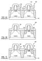
- FIG. 1A is a simplified cross section of a prior art CMOS cell 100 .
- the CMOS cell includes an NMOS transistor and a PMOS transistor fabricated on a silicon wafer substrate 101 .
- the NMOS transistor is separated from the PMOS transistor by a dielectric-filled isolation trench 103 .
- a tensile silicon nitride layer 102 overlies the source 104 , gate 106 and drain 108 regions of the NMOS transistor, and a compressive silicon nitride layer 112 overlies the source 114 , gate 116 , and drain 118 regions of the PMOS transistor.
- the tensile silicon nitride layer 102 produces tensile strain in the channel 110 of the NMOS transistor, and the compressive silicon nitride layer 112 produces compressive strain in the channel 120 of the PMOS transistor, each of which enhances charge carrier mobility.
- the tensile silicon nitride layer is deposited and selectively etched, and then the compressive silicon nitride layer is deposited and selectively etched, or vice versa.
- FIG. 1B is a simplified cross section of a prior art CMOS cell 130 having a tensile silicon nitride layer 132 formed over both the NMOS transistor and the PMOS transistor.
- the PMOS transistor includes silicon-germanium (SiGe) refilled source and drain 134 , 136 formed by selective epitaxy in cavities etched into the source and drain regions of the PMOS transistor.
- the SiGe plugs provide compressive stress; however, the compressive strain provided to the channel 138 is undesirably reduced by the overlying tensile silicon nitride layer 132 .
- FIG. 1C is a simplified cross section of a prior art CMOS cell 150 having a tensile silicon nitride layer 152 formed over both the NMOS transistor and a PMOS transistor, and having extended SiGe plugs 154 , 156 .
- the extended SiGe plugs 154 , 156 are epitaxially grown to extend above the original surface 157 of the silicon wafer substrate 101 . This provides additional compressive stress and also moves the tensile silicon nitride layer 152 further from the channel 158 of the PMOS transistor, thus avoiding some of the reduction of strain that occurs in the PMOS transistor of FIG. 1B .
- Recesses are formed in the drain and source regions of an MOS transistor.
- An ohmic contact layer is formed in the recesses, and a stressed silicon-nitride layer is formed over the ohmic contact layer.
- the recesses allow the stressed silicon nitride layer to provide strain in the plane of the channel region.
- a tensile silicon nitride layer is formed over recesses of an NMOS transistor in a CMOS cell, and a compressive silicon nitride layer is formed over recesses of a PMOS transistor in the CMOS cell.
- the stressed silicon nitride layer(s) is a chemical etch stop layer.
- FIG. 1A is a simplified cross section of a prior art CMOS cell.
- FIG. 1B is a simplified cross section of a prior art CMOS cell having a tensile silicon nitride layer formed over both the NMOS transistor and the PMOS transistor.
- FIG. 1C is a simplified cross section of a prior art CMOS cell having a tensile silicon nitride layer formed over both the NMOS transistor and the PMOS transistor, and having extended SiGe plugs.
- FIG. 2A is a simplified cross section of an MOS transistor according to an embodiment of the invention.
- FIG. 2B is a simplified cross section of a CMOS cell according to an embodiment of the invention.
- FIGS. 3A-3F are a series of cross sectional views illustrating steps of forming a transistor according to an embodiment of the invention.
- FIG. 4A is a flow chart of a method of fabricating a MOS transistor according to an embodiment of the invention.
- FIG. 4B is a flow chart of a method of fabricating a CMOS cell according to an embodiment of the invention.
- FIG. 2A is a simplified cross section of an MOS transistor 200 according to an embodiment of the invention.
- the MOS transistor 200 is fabricated on a substrate 202 , such as a silicon wafer or a silicon-on-insulator (SOI) wafer.
- a substrate 202 such as a silicon wafer or a silicon-on-insulator (SOI) wafer.
- SOI silicon-on-insulator
- many transistors are fabricated on a piece of the substrate, commonly called a die or chip.
- Transistors on a chip are often separated by trench isolation dielectric 204 or other isolation structures.
- a gate 206 is isolated from a channel 208 by a gate dielectric layer 210 .
- Sidewall spacers 212 align lightly-doped regions 214 , 216 with the source 218 and drain 220 .
- the source 218 , drain 220 , channel 208 , and lightly-doped regions 214 , 216 are formed in a well 221 of the substrate 202 .
- the well 221 is a P-well or N-well depending on whether the MOS transistor is an NMOS or PMOS transistor.
- the gate 206 is typically made of silicon (e.g., poly silicon), and an ohmic contact layer, such as a silicide layer, 222 is formed over the gate silicon.
- Ohmic contact layers 224 , 226 such as silicide layers, are similarly formed over the source 218 and drain 220 to facilitate electrically coupling these regions using metal traces or vias.
- the ohmic contact layers 224 , 226 are formed in recesses (see FIG. 3B , ref. num. 320 , 322 ) over the source 218 and drain 220 regions.
- a stressed silicon nitride layer 230 covers the MOS transistor from the source region to the drain region and fills the recesses. If the MOS transistor is an NMOS transistor, the stressed silicon nitride layer is a tensile layer, and if the MOS transistor is a PMOS transistor, the stressed silicon nitride layer is a compressive layer. This produces tensile and compressive strain, respectively, in the channel of the MOS transistor.
- Forming a recess that results in the bottom of the stressed silicon nitride layer to be beneath the top of the channel allows the stress to be applied directly across the channel (i.e., in the direction between the source and the drain). This in turn produces greater strain in the silicon of the channel, improving carrier mobility.
- Silicon nitride layers are typically used in CMOS fabrication sequences, so no new process steps, such as selective epitaxial growth of SiGe used in prior art devices, need to be added. The wafer does not have to be removed from the CMOS production sequence, which reduces yield loss due to contamination.
- the stressed silicon nitride layer is an etch stop layer provided between the MOS transistor and an overlying inter-metal dielectric (“IMD”) layer 232 .
- IMD inter-metal dielectric
- An IMD layer is typically deposited as a relatively thick layer, and subsequently flattened and reduced to a final thickness using a chemical-mechanical polish (“CMP”) technique.
- CMP chemical-mechanical polish
- the silicon nitride cap layer is used as an etch-stop layer when etching vias through the IMD layer, for example.
- the IMD layer 232 is also a stressed layer.
- the stressed silicon nitride layer is a compressive layer and the IMD layer is also a compressive layer, or both layers are tensile layers.
- the IMD layer has a first type of stress (e.g., compressive or tensile), and the stressed silicon nitride layer has a second type of stress (e.g., tensile or compressive). Stress in IMD layers can be induced by ion implantation, for example, so that a single IMD layer can be deposited, and stress induced in selected areas of the IMD layer.
- FIG. 2B is a simplified cross section of a CMOS cell 240 according to an embodiment of the invention.
- the CMOS cell 240 includes an NMOS transistor and a PMOS transistor separated by a dielectric-filled isolation trench 242 .
- Each of the NMOS transistor and PMOS transistor is similar to the MOS transistor of FIG. 2A and a detailed description of each half of the CMOS cell is omitted.
- a tensile silicon nitride layer 244 is formed over the NMOS transistor and a compressive silicon nitride layer 246 is formed over the PMOS transistor.
- An IMD layer 248 is typically formed over the stressed SiN layers 244 , 246 .
- the IMD layer is a neutral-stress layer.
- the IMD layer is a compressive-stress layer or a tensile-stress layer.
- the IMD layer has a tensile portion 250 overlying the tensile SiN layer and a compressive portion 252 overlying the compressive SiN layer.
- the IMD layer is deposited as a tensile layer, and selectively converted to a compressive layer over the PMOS cells, such as by ion implantation using the P-well mask, or vice versa.
- the IMD layer is deposited as a neutral-stress layer, and portions are converted to provide compressive and/or tensile stress.
- the N-well mask may be used to define the tensile and compressive silicon nitride layers.
- a P-well mask may be used. These layers are shown as being continuous, separated by a border represented by dashed line 245 . In practice, a small gap or overlap may occur due to mask alignment tolerances.
- an additional mask is used to form tensile and compressive silicon nitride layers that are separated from each other; however, using the N-well mask (or P-well mask) advantageously insures that stressed silicon nitride is formed over the entire source and drain regions and avoids having to generate the additional mask.
- the portion of the stressed silicon nitride layer in the recess pushes against the trench dielectric opposite the channel region.
- FIGS. 3A-3F are a series of cross sectional views illustrating steps of forming a transistor according to an embodiment of the invention.
- FIG. 3A shows a cross section of a partially fabricated transistor 300 , which in this example is a MOS transistor, such as a PMOS transistor or an NMOS transistor.
- a well 301 such as a P-well or an N-well, has been fabricated in the substrate 303 , which is a silicon wafer, silicon-on-insulator wafer, or similar substrate.
- a gate 302 is separated from a channel region 304 by a gate dielectric layer 306 .
- “Lightly doped drain” (“LDD”) regions 308 , 310 have been formed in source and drain areas.
- LDD Lightly doped drain
- First sidewall spacers 316 , 318 have been formed adjacent to gate 302 .
- Second sidewall spacers 312 , 314 have been formed on first sidewall spacers 316 , 318 .
- first sidewall spacers are omitted.
- FIG. 3B shows the partially fabricated transistor with recesses 320 , 322 .
- the recesses remove silicon from the source/drain regions below the original surface 324 of the substrate. In other words, the surfaces 326 , 328 of the recesses are below the original surface 324 of the substrate.
- the recesses 320 , 322 are aligned to the second sidewall spacers 312 , 314 and etched to a depth that does not extend through the LLD regions. Alternatively, the recesses are etched through the LDD regions.
- the recesses are formed using an anisotropic silicon etch process that aligns the sidewall of the recess with the edge of the outermost sidewall spacer.
- FIG. 3C shows the partially fabricated transistor after the source/drain implant and drive-in.
- the source/drain implant forms source and drain regions 330 , 332 that are more highly doped than the LDD regions 308 , 310 .
- FIG. 3D shows the partially fabricated transistor after a silicidation or other ohmic contact process.
- an ohmic contact layer 334 is a silicide layer formed on areas of exposed silicon, including the polysilicon gate 302 , and the source and drain regions 330 , 332 .
- the silicide layer provides a reliable, non-rectifying electrical contact from the underlying silicon to an overlying metal layer(s) (not shown).
- Other types of ohmic contact layers are alternatively used.
- FIG. 3E shows the partially fabricated transistor after a stressed silicon-nitride (“SiN”) layer 336 has been formed over the transistor.
- the stressed SiN layer 336 is formed so as to have a residual stress that induces strain that promotes carrier mobility in the channel region 304 .
- the transistor is an NMOS transistor
- the stressed SiN layer is formed to have residual tensile stress, producing tensile strain in the channel region
- the transistor is a PMOS transistor
- the stressed SiN layer is formed to have residual compressive stress, producing compressive strain in the channel region.
- the SiN layer 336 fills the recesses (see FIG. 3B , ref. nums. 320 , 322 ). This provides stressed layers on opposite sides of the channel region 304 . In particular, the SiN layer 336 pulls (if tensile) or presses against (if compressive) the sidewalls 338 , 340 of the silicon exposed when the recesses were formed. This transfers stress in the desired plane, namely across the channel region 304 , compared to a conventional stress layer that sits on top of the original surface of the silicon wafer (refer to FIG. 3B , ref. num. 324 ). Note that in FIG.
- the isolation dielectric extends above the original surface of the silicon wafer; however, by virtue of forming the recesses, the stressed SiN layer would pull/push against the sidewalls of the isolation dielectric even if the top of the isolation dielectric was even with the original surface of the silicon wafer.
- the stressed SiN layer also serves as a chemical etch-stop layer (“CESL”).
- CESLs are included in many CMOS fabrication sequences to provide a barrier to an etch through an overlying IMD layer, which is typically a very thick (relative to other layers in the MOS transistor) layer of silicon oxide.
- a stressed SiN CESL rather than a conventional SiN CESL, provides the advantage of increased carrier mobility in the channel region without adding another process, although the SiN deposition process is varied slightly to produce SiN layers having the desired type of stress. This is desirable because it avoids contamination problems that can arise when other stress-forming techniques, such as selective epitaxial growth, are used that are not normally part of a CMOS process flow.
- FIG. 3F shows the partially fabricated transistor after an IMD layer 350 has been formed over the stressed SiN layer 336 .
- the IMD layer is a stressed layer.
- the IMD layer does not have significant residual stress.
- a stressed IMD layer can have the same type of stress (e.g., tensile or compressive) as the underlying stressed SiN layer, or can have the opposite type of stress as the underlying stressed SiN layer.
- FIG. 4A is a flow chart of a method of fabricating a MOS transistor 400 according to an embodiment of the invention.
- the terms “PMOS transistor” and “NMOS transistor” are used for simplicity of illustration to describe a device during any portion of its fabrication sequence, as well as the finished transistors. Many common steps familiar to those of skill in the art of MOS transistor fabrication are omitted for clarity of discussion.
- Sidewall spacers are formed on the sides of a gate (step 402 ). In a particular embodiment, the sidewall spacers are oxide spacers having a thickness between about 5 nanometers and about 200 nanometers.
- An anisotropic silicon etch is performed in the source and drain regions of the MOS transistor (step 404 ) to form recesses.
- the anisotropic silicon etch is self-aligned to the sidewall spacers.
- the recesses are etched to a depth of between about 5 nanometers and about 50 nanometers.
- An isotropic etch is optionally performed if undercutting of the first sidewall spacers is desired.
- a halo implant, extension implant, and/or LDD implant are typically performed before the recesses are etched, but are alternatively performed after the recesses are etched.
- the halo implant is more localized than in a conventional device without recesses, whether it is performed before or after formation of the recesses, as long as halo thermal activation is after the formation of the recesses. This localized halo improves short channel effect and device performance.
- An ohmic contact layer is formed over the source and drain regions (step 406 ), and typically also over the gate at the same time.
- the ohmic contact layer is a silicide layer formed by depositing a suitable silicide-forming metal, followed by a thermal treatment.
- a stressed SiN layer is formed over at least the portions of the recesses adjacent to the gate (step 408 ), and typically over essentially the entire transistor, so as to fill the recesses above the ohmic contact layer with stressed SiN.
- the stressed SiN layer is about 40 nanometers to about 150 nanometers thick and also serves as a CESL.
- the SiN layer is sufficiently thick and sufficiently stressed so as to provide an increase in carrier mobility.
- an IMD layer is formed over the stressed SiN layer (step 410 ).
- the IMD layer is a second stressed layer.
- FIG. 4B is a flow chart of a method of fabricating a CMOS cell 420 according to an embodiment of the invention. Many common steps familiar to those of skill in the art of MOS transistor fabrication are omitted for clarity of discussion.
- Sidewall spacers are formed on the sides of the gates (step 422 ). In a particular embodiment, the sidewall spacers are oxide spacers having a thickness between about 5 nanometers and about 200 nanometers.
- An anisotropic silicon etch is performed in the source and drain regions of both MOS transistors (step 424 ) to form recesses. The anisotropic silicon etch is self-aligned to the sidewall spacers on each device.
- the recesses are etched to a depth of between about 5 nanometers and about 50 nanometers.
- An isotropic etch is optionally performed if undercutting of the first sidewall spacers is desired.
- Halo implants, extension implants, and/or LDD implants are typically performed before the recesses are etched, but are alternatively performed after the recesses are etched.
- the halo implants are more localized than in a conventional device without recesses, whether it is performed before or after formation of the recesses, as long as halo thermal activation is after the formation of the recesses. This localized halo improves short channel effect and device performance.
- An ohmic contact layer is formed over the source and drain regions of both MOS transistors (step 426 ), and typically also over the gates at the same time.
- the ohmic contact layer is a silicide layer formed by depositing a suitable silicide-forming metal, followed by a thermal treatment.
- a first stressed SiN layer having a first stress type is formed over at least the portions of the recesses adjacent to the gate of a first MOS transistor (step 428 ) so as to fill the portions of the recesses next to the gate of the first MOS transistor above the ohmic contact layer with a first type of stressed SiN.
- the first MOS transistor is the PMOS portion of the CMOS cell, and the first stressed SiN layer is a compressive SiN layer.
- the first MOS transistor is the NMOS portion of the CMOS cell and the first stressed SiN layer is a tensile SiN layer.
- the N-well mask is used to define where the first stressed SiN layer is deposited.
- the first stressed SiN layer is about 40 nanometers to about 150 nanometers thick and also serves as a CESL.
- a second stressed SiN layer having a second stress type (e.g., compressive or tensile) opposite the first stress type is formed over at least the portions of the recesses next to the gate of the second MOS transistor (step 430 ), and typically over essentially the entire transistor, so as to fill the portions of the recesses next to the gate above the ohmic contact layer with a second type of stressed SiN.
- the second stressed SiN layer is about 40 nanometers to about 150 nanometers thick and also serves as a CESL.
- the second stressed SiN layer and the adjoining first stressed SiN layer overlie isolation dielectric.
- an IMD layer is formed over the stressed SiN layer (step 432 ).
- the IMD layer is a stressed IMD layer having a first selected type of stress.
- selected portions of the stressed IMD layer are converted to a second selected type of stress (step 434 ).
Abstract
Description
Claims (19)
Priority Applications (2)
| Application Number | Priority Date | Filing Date | Title |
|---|---|---|---|
| US11/146,640 US7423283B1 (en) | 2005-06-07 | 2005-06-07 | Strain-silicon CMOS using etch-stop layer and method of manufacture |
| US12/200,851 US7875543B1 (en) | 2005-06-07 | 2008-08-28 | Strain-silicon CMOS using etch-stop layer and method of manufacture |
Applications Claiming Priority (1)
| Application Number | Priority Date | Filing Date | Title |
|---|---|---|---|
| US11/146,640 US7423283B1 (en) | 2005-06-07 | 2005-06-07 | Strain-silicon CMOS using etch-stop layer and method of manufacture |
Related Child Applications (1)
| Application Number | Title | Priority Date | Filing Date |
|---|---|---|---|
| US12/200,851 Division US7875543B1 (en) | 2005-06-07 | 2008-08-28 | Strain-silicon CMOS using etch-stop layer and method of manufacture |
Publications (1)
| Publication Number | Publication Date |
|---|---|
| US7423283B1 true US7423283B1 (en) | 2008-09-09 |
Family
ID=39734332
Family Applications (2)
| Application Number | Title | Priority Date | Filing Date |
|---|---|---|---|
| US11/146,640 Active US7423283B1 (en) | 2005-06-07 | 2005-06-07 | Strain-silicon CMOS using etch-stop layer and method of manufacture |
| US12/200,851 Expired - Fee Related US7875543B1 (en) | 2005-06-07 | 2008-08-28 | Strain-silicon CMOS using etch-stop layer and method of manufacture |
Family Applications After (1)
| Application Number | Title | Priority Date | Filing Date |
|---|---|---|---|
| US12/200,851 Expired - Fee Related US7875543B1 (en) | 2005-06-07 | 2008-08-28 | Strain-silicon CMOS using etch-stop layer and method of manufacture |
Country Status (1)
| Country | Link |
|---|---|
| US (2) | US7423283B1 (en) |
Cited By (12)
| Publication number | Priority date | Publication date | Assignee | Title |
|---|---|---|---|---|
| US20080029831A1 (en) * | 2006-08-01 | 2008-02-07 | Taiwan Semiconductor Manufacturing Company, Ltd. | CMOS devices with graded silicide regions |
| US20080284462A1 (en) * | 2005-09-06 | 2008-11-20 | Victor Chan | Mechanical stress characterization in semiconductor device |
| US20080293194A1 (en) * | 2007-05-24 | 2008-11-27 | Neng-Kuo Chen | Method of making a P-type metal-oxide semiconductor transistor and method of making a complementary metal-oxide semiconductor transistor |
| US7655991B1 (en) * | 2005-09-08 | 2010-02-02 | Xilinx, Inc. | CMOS device with stressed sidewall spacers |
| US7670923B1 (en) | 2005-03-31 | 2010-03-02 | Xilinx, Inc. | Method of fabricating strain-silicon CMOS |
| US20100144105A1 (en) * | 2008-12-08 | 2010-06-10 | Advanced Micro Devices, Inc. | Methods for fabricating stressed mos devices |
| US20100193870A1 (en) * | 2009-01-30 | 2010-08-05 | Xilinx, Inc. | Techniques for improving transistor-to-transistor stress uniformity |
| US7875543B1 (en) | 2005-06-07 | 2011-01-25 | Xilinx, Inc. | Strain-silicon CMOS using etch-stop layer and method of manufacture |
| US7936006B1 (en) | 2005-10-06 | 2011-05-03 | Xilinx, Inc. | Semiconductor device with backfilled isolation |
| US20130140644A1 (en) * | 2005-05-19 | 2013-06-06 | Kabushiki Kaisha Toshiba | Method of manufacturing semiconductor device |
| US20150028431A1 (en) * | 2011-04-04 | 2015-01-29 | Globalfoundries Inc. | Mol insitu pt rework sequence |
| CN105470238A (en) * | 2014-09-09 | 2016-04-06 | 中芯国际集成电路制造(上海)有限公司 | Electrical programmable fuse device, integrated circuit and electronic device |
Families Citing this family (5)
| Publication number | Priority date | Publication date | Assignee | Title |
|---|---|---|---|---|
| JP5168274B2 (en) * | 2007-05-14 | 2013-03-21 | 富士通セミコンダクター株式会社 | Manufacturing method of semiconductor device |
| CN103367364B (en) * | 2012-03-27 | 2015-12-09 | 中国科学院微电子研究所 | CMOS and manufacture method thereof |
| CA2893828A1 (en) | 2012-12-14 | 2015-06-03 | Bhc Technology Holdings Llc | Point of care isolation and concentration of blood cells |
| US9196613B2 (en) | 2013-11-19 | 2015-11-24 | International Business Machines Corporation | Stress inducing contact metal in FinFET CMOS |
| KR102434914B1 (en) | 2016-01-15 | 2022-08-23 | 삼성전자주식회사 | Method for forming patterns of semiconductor device and method for fabricating semiconductor device using the same |
Citations (33)
| Publication number | Priority date | Publication date | Assignee | Title |
|---|---|---|---|---|
| US5989986A (en) | 1997-03-13 | 1999-11-23 | United Microelectronics Corp. | Method to inhibit the formation of ion implantation induced edge defects |
| US6075262A (en) | 1995-09-21 | 2000-06-13 | Fujitsu Limited | Semiconductor device having T-shaped gate electrode |
| US6177319B1 (en) | 1999-01-16 | 2001-01-23 | United Microelectronics Corp. | Method of manufacturing salicide layer |
| US6262445B1 (en) | 1998-03-30 | 2001-07-17 | Texas Instruments Incorporated | SiC sidewall process |
| US6306712B1 (en) | 1997-12-05 | 2001-10-23 | Texas Instruments Incorporated | Sidewall process and method of implantation for improved CMOS with benefit of low CGD, improved doping profiles, and insensitivity to chemical processing |
| US6399973B1 (en) | 2000-12-29 | 2002-06-04 | Intel Corporation | Technique to produce isolated junctions by forming an insulation layer |
| US6541343B1 (en) | 1999-12-30 | 2003-04-01 | Intel Corporation | Methods of making field effect transistor structure with partially isolated source/drain junctions |
| US6563152B2 (en) | 2000-12-29 | 2003-05-13 | Intel Corporation | Technique to obtain high mobility channels in MOS transistors by forming a strain layer on an underside of a channel |
| US6573172B1 (en) * | 2002-09-16 | 2003-06-03 | Advanced Micro Devices, Inc. | Methods for improving carrier mobility of PMOS and NMOS devices |
| US6713360B2 (en) | 2001-12-28 | 2004-03-30 | Texas Instruments Incorporated | System for reducing segregation and diffusion of halo implants into highly doped regions |
| US6743684B2 (en) | 2002-10-11 | 2004-06-01 | Texas Instruments Incorporated | Method to produce localized halo for MOS transistor |
| US20040104405A1 (en) | 2002-12-02 | 2004-06-03 | Taiwan Semiconductor Manufacturing Company | Novel CMOS device |
| US20050040460A1 (en) | 2002-12-12 | 2005-02-24 | Dureseti Chidambarrao | Stress inducing spacers |
| US6870179B2 (en) | 2003-03-31 | 2005-03-22 | Intel Corporation | Increasing stress-enhanced drive current in a MOS transistor |
| US20050136606A1 (en) | 2003-12-19 | 2005-06-23 | Hartmut Rulke | Spacer for a gate electrode having tensile stress and a method of forming the same |
| US6939814B2 (en) * | 2003-10-30 | 2005-09-06 | International Business Machines Corporation | Increasing carrier mobility in NFET and PFET transistors on a common wafer |
| US20050247986A1 (en) | 2004-05-06 | 2005-11-10 | Taiwan Semiconductor Manufacturing Co., Ltd. | Offset spacer formation for strained channel CMOS transistor |
| US20050247975A1 (en) | 2004-04-23 | 2005-11-10 | Jea-Hee Kim | Semiconductor devices and methods of manufacturing the same |
| US20060009041A1 (en) | 2004-07-06 | 2006-01-12 | Iyer R S | Silicon nitride film with stress control |
| US20060014350A1 (en) | 2004-07-18 | 2006-01-19 | Yun-Ren Wang | Method for fabricating a semiconductor transistor device having ultra-shallow source/drain extensions |
| US7052964B2 (en) * | 2003-04-25 | 2006-05-30 | Taiwan Semiconductor Manufacturing Company, Ltd. | Strained channel transistor and methods of manufacture |
| US7053400B2 (en) * | 2004-05-05 | 2006-05-30 | Advanced Micro Devices, Inc. | Semiconductor device based on Si-Ge with high stress liner for enhanced channel carrier mobility |
| US20060189167A1 (en) * | 2005-02-18 | 2006-08-24 | Hsiang-Ying Wang | Method for fabricating silicon nitride film |
| US20060244074A1 (en) | 2005-04-29 | 2006-11-02 | Chien-Hao Chen | Hybrid-strained sidewall spacer for CMOS process |
| US7132704B2 (en) | 2003-04-30 | 2006-11-07 | Freescale Semiconductor, Inc. | Transistor sidewall spacer stress modulation |
| US20070001217A1 (en) | 2005-06-29 | 2007-01-04 | Shang-Chih Chen | Closed loop CESL high performance CMOS devices |
| US20070034963A1 (en) | 2005-08-10 | 2007-02-15 | Toshiba America Electronic Components, Inc. | Semiconductor device with close stress liner film and method of manufacturing the same |
| US7193254B2 (en) | 2004-11-30 | 2007-03-20 | International Business Machines Corporation | Structure and method of applying stresses to PFET and NFET transistor channels for improved performance |
| US7208362B2 (en) | 2003-06-25 | 2007-04-24 | Texas Instruments Incorporated | Transistor device containing carbon doped silicon in a recess next to MDD to create strain in channel |
| US7256084B2 (en) | 2005-05-04 | 2007-08-14 | Chartered Semiconductor Manufacturing Ltd. | Composite stress spacer |
| US7259105B2 (en) | 2003-12-31 | 2007-08-21 | Dongbu Electronics Co., Ltd. | Methods of fabricating gate spacers for semiconductor devices |
| US7288448B2 (en) | 2004-08-24 | 2007-10-30 | Orlowski Marius K | Method and apparatus for mobility enhancement in a semiconductor device |
| US7314793B2 (en) * | 2004-05-28 | 2008-01-01 | Advanced Micro Devices, Inc. | Technique for controlling mechanical stress in a channel region by spacer removal |
Family Cites Families (22)
| Publication number | Priority date | Publication date | Assignee | Title |
|---|---|---|---|---|
| US4894694A (en) | 1986-10-31 | 1990-01-16 | Hewlett-Packard Company | MOSFET structure and method for making same |
| US4985744A (en) | 1988-01-29 | 1991-01-15 | Texas Instruments Incorporated | Method for forming a recessed contact bipolar transistor and field effect transistor |
| US5650340A (en) | 1994-08-18 | 1997-07-22 | Sun Microsystems, Inc. | Method of making asymmetric low power MOS devices |
| JP3604791B2 (en) | 1995-11-09 | 2004-12-22 | 株式会社ルネサステクノロジ | Method for manufacturing semiconductor device |
| KR100214468B1 (en) | 1995-12-29 | 1999-08-02 | 구본준 | Method for fabricating cmos |
| JP3305211B2 (en) | 1996-09-10 | 2002-07-22 | 松下電器産業株式会社 | Semiconductor device and manufacturing method thereof |
| US6287988B1 (en) | 1997-03-18 | 2001-09-11 | Kabushiki Kaisha Toshiba | Semiconductor device manufacturing method, semiconductor device manufacturing apparatus and semiconductor device |
| US5989966A (en) | 1997-12-15 | 1999-11-23 | Taiwan Semiconductor Manufacturing Company, Ltd. | Method and a deep sub-micron field effect transistor structure for suppressing short channel effects |
| US6995430B2 (en) | 2002-06-07 | 2006-02-07 | Amberwave Systems Corporation | Strained-semiconductor-on-insulator device structures |
| JP2004172389A (en) | 2002-11-20 | 2004-06-17 | Renesas Technology Corp | Semiconductor device and method for manufacturing the same |
| KR101088712B1 (en) | 2004-05-03 | 2011-12-01 | 동부일렉트로닉스 주식회사 | Method for manufacturing semiconductor device |
| US7227205B2 (en) | 2004-06-24 | 2007-06-05 | International Business Machines Corporation | Strained-silicon CMOS device and method |
| JP4081071B2 (en) | 2004-11-26 | 2008-04-23 | 株式会社東芝 | Semiconductor memory device and manufacturing method thereof |
| US7138309B2 (en) | 2005-01-19 | 2006-11-21 | Sharp Laboratories Of America, Inc. | Integration of biaxial tensile strained NMOS and uniaxial compressive strained PMOS on the same wafer |
| US7429775B1 (en) | 2005-03-31 | 2008-09-30 | Xilinx, Inc. | Method of fabricating strain-silicon CMOS |
| US20060267106A1 (en) | 2005-05-26 | 2006-11-30 | Taiwan Semiconductor Manufacturing Company, Ltd. | Novel semiconductor device with improved channel strain effect |
| US7423283B1 (en) | 2005-06-07 | 2008-09-09 | Xilinx, Inc. | Strain-silicon CMOS using etch-stop layer and method of manufacture |
| US7528028B2 (en) | 2005-06-17 | 2009-05-05 | Taiwan Semiconductor Manufacturing Company, Ltd. | Super anneal for process induced strain modulation |
| US7494858B2 (en) | 2005-06-30 | 2009-02-24 | Intel Corporation | Transistor with improved tip profile and method of manufacture thereof |
| US20070010073A1 (en) | 2005-07-06 | 2007-01-11 | Chien-Hao Chen | Method of forming a MOS device having a strained channel region |
| DE102005052054B4 (en) | 2005-10-31 | 2010-08-19 | Advanced Micro Devices, Inc., Sunnyvale | Semiconductor device with shaped channel region transistors and method of making the same |
| DE102006015090B4 (en) * | 2006-03-31 | 2008-03-13 | Advanced Micro Devices, Inc., Sunnyvale | Method for producing different embedded deformation layers in transistors |
-
2005
- 2005-06-07 US US11/146,640 patent/US7423283B1/en active Active
-
2008
- 2008-08-28 US US12/200,851 patent/US7875543B1/en not_active Expired - Fee Related
Patent Citations (33)
| Publication number | Priority date | Publication date | Assignee | Title |
|---|---|---|---|---|
| US6075262A (en) | 1995-09-21 | 2000-06-13 | Fujitsu Limited | Semiconductor device having T-shaped gate electrode |
| US5989986A (en) | 1997-03-13 | 1999-11-23 | United Microelectronics Corp. | Method to inhibit the formation of ion implantation induced edge defects |
| US6306712B1 (en) | 1997-12-05 | 2001-10-23 | Texas Instruments Incorporated | Sidewall process and method of implantation for improved CMOS with benefit of low CGD, improved doping profiles, and insensitivity to chemical processing |
| US6262445B1 (en) | 1998-03-30 | 2001-07-17 | Texas Instruments Incorporated | SiC sidewall process |
| US6177319B1 (en) | 1999-01-16 | 2001-01-23 | United Microelectronics Corp. | Method of manufacturing salicide layer |
| US6541343B1 (en) | 1999-12-30 | 2003-04-01 | Intel Corporation | Methods of making field effect transistor structure with partially isolated source/drain junctions |
| US6563152B2 (en) | 2000-12-29 | 2003-05-13 | Intel Corporation | Technique to obtain high mobility channels in MOS transistors by forming a strain layer on an underside of a channel |
| US6399973B1 (en) | 2000-12-29 | 2002-06-04 | Intel Corporation | Technique to produce isolated junctions by forming an insulation layer |
| US6713360B2 (en) | 2001-12-28 | 2004-03-30 | Texas Instruments Incorporated | System for reducing segregation and diffusion of halo implants into highly doped regions |
| US6573172B1 (en) * | 2002-09-16 | 2003-06-03 | Advanced Micro Devices, Inc. | Methods for improving carrier mobility of PMOS and NMOS devices |
| US6743684B2 (en) | 2002-10-11 | 2004-06-01 | Texas Instruments Incorporated | Method to produce localized halo for MOS transistor |
| US20040104405A1 (en) | 2002-12-02 | 2004-06-03 | Taiwan Semiconductor Manufacturing Company | Novel CMOS device |
| US20050040460A1 (en) | 2002-12-12 | 2005-02-24 | Dureseti Chidambarrao | Stress inducing spacers |
| US6870179B2 (en) | 2003-03-31 | 2005-03-22 | Intel Corporation | Increasing stress-enhanced drive current in a MOS transistor |
| US7052964B2 (en) * | 2003-04-25 | 2006-05-30 | Taiwan Semiconductor Manufacturing Company, Ltd. | Strained channel transistor and methods of manufacture |
| US7132704B2 (en) | 2003-04-30 | 2006-11-07 | Freescale Semiconductor, Inc. | Transistor sidewall spacer stress modulation |
| US7208362B2 (en) | 2003-06-25 | 2007-04-24 | Texas Instruments Incorporated | Transistor device containing carbon doped silicon in a recess next to MDD to create strain in channel |
| US6939814B2 (en) * | 2003-10-30 | 2005-09-06 | International Business Machines Corporation | Increasing carrier mobility in NFET and PFET transistors on a common wafer |
| US20050136606A1 (en) | 2003-12-19 | 2005-06-23 | Hartmut Rulke | Spacer for a gate electrode having tensile stress and a method of forming the same |
| US7259105B2 (en) | 2003-12-31 | 2007-08-21 | Dongbu Electronics Co., Ltd. | Methods of fabricating gate spacers for semiconductor devices |
| US20050247975A1 (en) | 2004-04-23 | 2005-11-10 | Jea-Hee Kim | Semiconductor devices and methods of manufacturing the same |
| US7053400B2 (en) * | 2004-05-05 | 2006-05-30 | Advanced Micro Devices, Inc. | Semiconductor device based on Si-Ge with high stress liner for enhanced channel carrier mobility |
| US20050247986A1 (en) | 2004-05-06 | 2005-11-10 | Taiwan Semiconductor Manufacturing Co., Ltd. | Offset spacer formation for strained channel CMOS transistor |
| US7314793B2 (en) * | 2004-05-28 | 2008-01-01 | Advanced Micro Devices, Inc. | Technique for controlling mechanical stress in a channel region by spacer removal |
| US20060009041A1 (en) | 2004-07-06 | 2006-01-12 | Iyer R S | Silicon nitride film with stress control |
| US20060014350A1 (en) | 2004-07-18 | 2006-01-19 | Yun-Ren Wang | Method for fabricating a semiconductor transistor device having ultra-shallow source/drain extensions |
| US7288448B2 (en) | 2004-08-24 | 2007-10-30 | Orlowski Marius K | Method and apparatus for mobility enhancement in a semiconductor device |
| US7193254B2 (en) | 2004-11-30 | 2007-03-20 | International Business Machines Corporation | Structure and method of applying stresses to PFET and NFET transistor channels for improved performance |
| US20060189167A1 (en) * | 2005-02-18 | 2006-08-24 | Hsiang-Ying Wang | Method for fabricating silicon nitride film |
| US20060244074A1 (en) | 2005-04-29 | 2006-11-02 | Chien-Hao Chen | Hybrid-strained sidewall spacer for CMOS process |
| US7256084B2 (en) | 2005-05-04 | 2007-08-14 | Chartered Semiconductor Manufacturing Ltd. | Composite stress spacer |
| US20070001217A1 (en) | 2005-06-29 | 2007-01-04 | Shang-Chih Chen | Closed loop CESL high performance CMOS devices |
| US20070034963A1 (en) | 2005-08-10 | 2007-02-15 | Toshiba America Electronic Components, Inc. | Semiconductor device with close stress liner film and method of manufacturing the same |
Non-Patent Citations (11)
| Title |
|---|
| A. Brand et al., "Intel's 0.25 Micron, 2.0Volts Logic Process Technology", pp. 1-9, available from Intel Corportion (Santa Clara) Corporate Office, 2200 Mission College Blvd., Santa Clara, California 95052-8119, dated; 1998. |
| B. P. R. Chidambaram et al., "35% Drive Current Imporvement from Recessed-SiGe Drain Extensions on 37 nm Gate Length PMOS", 2004 Sumposium on VLSI Technology, Digest of Technical Paper, pp. 48-49, available form Texas Instruments, MS 3739, 13560 N. Central Expressway, Dallas, TX 75243; dated 2004. |
| Luo, Y. et al., "Enhancement of CMOS Performance by Process-Induced Stress", IEEE Transactions on Seminconductors Manufacturing, vol. 18, No. 1, Feb. 2006, pp. 63-68. |
| Min Chin Chai, "90 nm Node CMOS Technology Comparison between Intel Corporation and Samsung Electronics", pp. 1-6, May 8, 2003, available from Intel Corporation (Santa Clara) Corporate Office, 2200 Mission College Blvd., Santa Clara, California 95052-8119. |
| Nayak, Deepak Kumar et al., "CMOS Device With Stressed Sidewall Spacers", U.S. Appl. No. 11/221,507, filed Sep. 8, 2005, 17pages, available from Xilinx Inc., 2100 Logic Drive, San Jose, CA 95124. |
| Pidin, S. et al., "A Novel Strain Enhanced CMOS Architecture Using Selectively Deposited High Tensile and High Compressive Silicon Nitride Films", IEEE 2004, pp. 1-8, available from IEEE, 3 Park Avenue, 17th Floor, New York, NY 10016-5997. |
| T. Ghani et al., "A 90nm High Volume Manufacturing Logic Technology featuring Novel 45nm Gate Lenght Strained Silicon CMOS Transistors", IEEE, 2003, pp. 1-3, available from fahr.ghani@intel.com, or Intel Corporation (Santa Clara) Corporate Office, 2200 Mission College Blvd., Santa Clara, California 95052-8119, dated 2003. |
| Thompson, S. et al., A 90 nm Logic Technology Featuring 50 nm Strained Silicon Channel Transistors, 7 Layers Of Cu Interconnects, Low K ILD, and 1 um2 SRAM Cell, iedm 2002, pp. 1-32, available from Intel Corporation, www.intel.com/research/silicon. |
| U.S. Appl. No. 11/095,814, filed Mar. 31, 2005, Nayak et al. |
| U.S. Appl. No. 11/221,507, Nayak, D. K. et al., "CMOS Device With Sressed Sidewall Spacers", filed Sep. 8, 2005, 13 pages, available form Xilinx Inc., 2100 Logic Drive, San Jose CA 95124. |
| Yuhao Luo, et al., "Semiconductor Device with Backfilled Isolation", U.S. Appl. No. 11/244, 566, filed Oct. 6, 2005, 13 pages, available from Xilinx inc., 2100 Logic Drive, San Jose, CA 95124. |
Cited By (18)
| Publication number | Priority date | Publication date | Assignee | Title |
|---|---|---|---|---|
| US7670923B1 (en) | 2005-03-31 | 2010-03-02 | Xilinx, Inc. | Method of fabricating strain-silicon CMOS |
| US8878306B2 (en) * | 2005-05-19 | 2014-11-04 | Kabushiki Kaisha Toshiba | Semiconductor device |
| US20130140644A1 (en) * | 2005-05-19 | 2013-06-06 | Kabushiki Kaisha Toshiba | Method of manufacturing semiconductor device |
| US7875543B1 (en) | 2005-06-07 | 2011-01-25 | Xilinx, Inc. | Strain-silicon CMOS using etch-stop layer and method of manufacture |
| US20080284462A1 (en) * | 2005-09-06 | 2008-11-20 | Victor Chan | Mechanical stress characterization in semiconductor device |
| US7816909B2 (en) * | 2005-09-06 | 2010-10-19 | International Business Machines Corporation | Mechanical stress characterization in semiconductor device |
| US7655991B1 (en) * | 2005-09-08 | 2010-02-02 | Xilinx, Inc. | CMOS device with stressed sidewall spacers |
| US7936006B1 (en) | 2005-10-06 | 2011-05-03 | Xilinx, Inc. | Semiconductor device with backfilled isolation |
| US7545006B2 (en) * | 2006-08-01 | 2009-06-09 | Taiwan Semiconductor Manufacturing Company, Ltd. | CMOS devices with graded silicide regions |
| US20080029831A1 (en) * | 2006-08-01 | 2008-02-07 | Taiwan Semiconductor Manufacturing Company, Ltd. | CMOS devices with graded silicide regions |
| US20090280614A1 (en) * | 2007-05-24 | 2009-11-12 | Neng-Kuo Chen | Method of making a P-type metal-oxide semiconductor transistor and method of making a complementary metal-oxide semiconductor transistor |
| US20080293194A1 (en) * | 2007-05-24 | 2008-11-27 | Neng-Kuo Chen | Method of making a P-type metal-oxide semiconductor transistor and method of making a complementary metal-oxide semiconductor transistor |
| US7977180B2 (en) * | 2008-12-08 | 2011-07-12 | GlobalFoundries, Inc. | Methods for fabricating stressed MOS devices |
| US20100144105A1 (en) * | 2008-12-08 | 2010-06-10 | Advanced Micro Devices, Inc. | Methods for fabricating stressed mos devices |
| US7932563B2 (en) * | 2009-01-30 | 2011-04-26 | Xilinx, Inc. | Techniques for improving transistor-to-transistor stress uniformity |
| US20100193870A1 (en) * | 2009-01-30 | 2010-08-05 | Xilinx, Inc. | Techniques for improving transistor-to-transistor stress uniformity |
| US20150028431A1 (en) * | 2011-04-04 | 2015-01-29 | Globalfoundries Inc. | Mol insitu pt rework sequence |
| CN105470238A (en) * | 2014-09-09 | 2016-04-06 | 中芯国际集成电路制造(上海)有限公司 | Electrical programmable fuse device, integrated circuit and electronic device |
Also Published As
| Publication number | Publication date |
|---|---|
| US7875543B1 (en) | 2011-01-25 |
Similar Documents
| Publication | Publication Date | Title |
|---|---|---|
| US7423283B1 (en) | Strain-silicon CMOS using etch-stop layer and method of manufacture | |
| US7429775B1 (en) | Method of fabricating strain-silicon CMOS | |
| US8350253B1 (en) | Integrated circuit with stress inserts | |
| US9362181B1 (en) | Methods of forming diffusion breaks on integrated circuit products comprised of FinFET devices and the resulting products | |
| US8497168B2 (en) | Structure and method to enhance both NFET and PFET performance using different kinds of stressed layers | |
| US6461900B1 (en) | Method to form a self-aligned CMOS inverter using vertical device integration | |
| US7687335B2 (en) | Self aligned gate JFET structure and method | |
| US7569447B2 (en) | Method of forming transistor structure having stressed regions of opposite types | |
| US20070096144A1 (en) | Integrated circuit using complementary junction field effect transistor and MOS transistor in silicon and silicon alloys | |
| US20020192911A1 (en) | Damascene double gated transistors and related manufacturing methods | |
| US7884002B2 (en) | Method of fabricating self aligned Schottky junctions for semiconductor devices | |
| KR20080114608A (en) | Semiconductor device and method for manufacturing semiconductor device | |
| US20080272394A1 (en) | Junction field effect transistors in germanium and silicon-germanium alloys and method for making and using | |
| US7473594B2 (en) | Raised STI structure and superdamascene technique for NMOSFET performance enhancement with embedded silicon carbon | |
| CN109273440B (en) | Method for manufacturing fin-shaped structure with tensile stress and complementary fin-shaped transistor structure | |
| US7936006B1 (en) | Semiconductor device with backfilled isolation | |
| KR20220084037A (en) | Method of Fabricating Charge Trap TFET Semiconductor Devices for Advanced Logic Operation | |
| US20030020120A1 (en) | Mosfet having a low aspect ratio between the gate and the source/drain | |
| US8183105B2 (en) | Integrated circuit device with stress reduction layer | |
| US20200083116A1 (en) | Gate, Contact, and Fin Cut Method | |
| US7429526B1 (en) | Method of forming silicide gate with interlayer | |
| US20170069755A1 (en) | Embedded sige process for multi-threshold pmos transistors | |
| US7655991B1 (en) | CMOS device with stressed sidewall spacers | |
| US20090258464A1 (en) | Methods for manufacturing a high voltage junction field effect transistor using a hybrid orientation technology wafer | |
| US20050151173A1 (en) | Semiconductor device and methods of manufacturing the same |
Legal Events
| Date | Code | Title | Description |
|---|---|---|---|
| AS | Assignment |
Owner name: XILINX, INC., CALIFORNIA Free format text: ASSIGNMENT OF ASSIGNORS INTEREST;ASSIGNORS:LUO, YUHAO;NAYAK, DEEPAK KUMAR;REEL/FRAME:016666/0660 Effective date: 20050603 |
|
| STCF | Information on status: patent grant |
Free format text: PATENTED CASE |
|
| FPAY | Fee payment |
Year of fee payment: 4 |
|
| FPAY | Fee payment |
Year of fee payment: 8 |
|
| MAFP | Maintenance fee payment |
Free format text: PAYMENT OF MAINTENANCE FEE, 12TH YEAR, LARGE ENTITY (ORIGINAL EVENT CODE: M1553); ENTITY STATUS OF PATENT OWNER: LARGE ENTITY Year of fee payment: 12 |