US7432750B1 - Methods and apparatus for frequency synthesis with feedback interpolation - Google Patents
Methods and apparatus for frequency synthesis with feedback interpolation Download PDFInfo
- Publication number
- US7432750B1 US7432750B1 US11/296,786 US29678605A US7432750B1 US 7432750 B1 US7432750 B1 US 7432750B1 US 29678605 A US29678605 A US 29678605A US 7432750 B1 US7432750 B1 US 7432750B1
- Authority
- US
- United States
- Prior art keywords
- clock
- circuit
- frequency
- interpolator
- control
- Prior art date
- Legal status (The legal status is an assumption and is not a legal conclusion. Google has not performed a legal analysis and makes no representation as to the accuracy of the status listed.)
- Expired - Fee Related
Links
Images


Classifications
-
- H—ELECTRICITY
- H03—ELECTRONIC CIRCUITRY
- H03L—AUTOMATIC CONTROL, STARTING, SYNCHRONISATION, OR STABILISATION OF GENERATORS OF ELECTRONIC OSCILLATIONS OR PULSES
- H03L7/00—Automatic control of frequency or phase; Synchronisation
- H03L7/06—Automatic control of frequency or phase; Synchronisation using a reference signal applied to a frequency- or phase-locked loop
- H03L7/08—Details of the phase-locked loop
- H03L7/085—Details of the phase-locked loop concerning mainly the frequency- or phase-detection arrangement including the filtering or amplification of its output signal
- H03L7/089—Details of the phase-locked loop concerning mainly the frequency- or phase-detection arrangement including the filtering or amplification of its output signal the phase or frequency detector generating up-down pulses
- H03L7/0891—Details of the phase-locked loop concerning mainly the frequency- or phase-detection arrangement including the filtering or amplification of its output signal the phase or frequency detector generating up-down pulses the up-down pulses controlling source and sink current generators, e.g. a charge pump
- H03L7/0893—Details of the phase-locked loop concerning mainly the frequency- or phase-detection arrangement including the filtering or amplification of its output signal the phase or frequency detector generating up-down pulses the up-down pulses controlling source and sink current generators, e.g. a charge pump the up-down pulses controlling at least two source current generators or at least two sink current generators connected to different points in the loop
-
- H—ELECTRICITY
- H03—ELECTRONIC CIRCUITRY
- H03K—PULSE TECHNIQUE
- H03K5/00—Manipulating of pulses not covered by one of the other main groups of this subclass
- H03K5/13—Arrangements having a single output and transforming input signals into pulses delivered at desired time intervals
- H03K5/133—Arrangements having a single output and transforming input signals into pulses delivered at desired time intervals using a chain of active delay devices
-
- H—ELECTRICITY
- H03—ELECTRONIC CIRCUITRY
- H03L—AUTOMATIC CONTROL, STARTING, SYNCHRONISATION, OR STABILISATION OF GENERATORS OF ELECTRONIC OSCILLATIONS OR PULSES
- H03L7/00—Automatic control of frequency or phase; Synchronisation
- H03L7/06—Automatic control of frequency or phase; Synchronisation using a reference signal applied to a frequency- or phase-locked loop
- H03L7/08—Details of the phase-locked loop
- H03L7/081—Details of the phase-locked loop provided with an additional controlled phase shifter
-
- H—ELECTRICITY
- H03—ELECTRONIC CIRCUITRY
- H03L—AUTOMATIC CONTROL, STARTING, SYNCHRONISATION, OR STABILISATION OF GENERATORS OF ELECTRONIC OSCILLATIONS OR PULSES
- H03L7/00—Automatic control of frequency or phase; Synchronisation
- H03L7/06—Automatic control of frequency or phase; Synchronisation using a reference signal applied to a frequency- or phase-locked loop
- H03L7/08—Details of the phase-locked loop
- H03L7/085—Details of the phase-locked loop concerning mainly the frequency- or phase-detection arrangement including the filtering or amplification of its output signal
- H03L7/089—Details of the phase-locked loop concerning mainly the frequency- or phase-detection arrangement including the filtering or amplification of its output signal the phase or frequency detector generating up-down pulses
- H03L7/0891—Details of the phase-locked loop concerning mainly the frequency- or phase-detection arrangement including the filtering or amplification of its output signal the phase or frequency detector generating up-down pulses the up-down pulses controlling source and sink current generators, e.g. a charge pump
- H03L7/0895—Details of the current generators
-
- H—ELECTRICITY
- H03—ELECTRONIC CIRCUITRY
- H03L—AUTOMATIC CONTROL, STARTING, SYNCHRONISATION, OR STABILISATION OF GENERATORS OF ELECTRONIC OSCILLATIONS OR PULSES
- H03L7/00—Automatic control of frequency or phase; Synchronisation
- H03L7/06—Automatic control of frequency or phase; Synchronisation using a reference signal applied to a frequency- or phase-locked loop
- H03L7/08—Details of the phase-locked loop
- H03L7/085—Details of the phase-locked loop concerning mainly the frequency- or phase-detection arrangement including the filtering or amplification of its output signal
- H03L7/093—Details of the phase-locked loop concerning mainly the frequency- or phase-detection arrangement including the filtering or amplification of its output signal using special filtering or amplification characteristics in the loop
-
- H—ELECTRICITY
- H03—ELECTRONIC CIRCUITRY
- H03L—AUTOMATIC CONTROL, STARTING, SYNCHRONISATION, OR STABILISATION OF GENERATORS OF ELECTRONIC OSCILLATIONS OR PULSES
- H03L7/00—Automatic control of frequency or phase; Synchronisation
- H03L7/06—Automatic control of frequency or phase; Synchronisation using a reference signal applied to a frequency- or phase-locked loop
- H03L7/08—Details of the phase-locked loop
- H03L7/099—Details of the phase-locked loop concerning mainly the controlled oscillator of the loop
- H03L7/0995—Details of the phase-locked loop concerning mainly the controlled oscillator of the loop the oscillator comprising a ring oscillator
- H03L7/0998—Details of the phase-locked loop concerning mainly the controlled oscillator of the loop the oscillator comprising a ring oscillator using phase interpolation
-
- H—ELECTRICITY
- H03—ELECTRONIC CIRCUITRY
- H03L—AUTOMATIC CONTROL, STARTING, SYNCHRONISATION, OR STABILISATION OF GENERATORS OF ELECTRONIC OSCILLATIONS OR PULSES
- H03L7/00—Automatic control of frequency or phase; Synchronisation
- H03L7/06—Automatic control of frequency or phase; Synchronisation using a reference signal applied to a frequency- or phase-locked loop
- H03L7/16—Indirect frequency synthesis, i.e. generating a desired one of a number of predetermined frequencies using a frequency- or phase-locked loop
- H03L7/18—Indirect frequency synthesis, i.e. generating a desired one of a number of predetermined frequencies using a frequency- or phase-locked loop using a frequency divider or counter in the loop
-
- H—ELECTRICITY
- H03—ELECTRONIC CIRCUITRY
- H03K—PULSE TECHNIQUE
- H03K5/00—Manipulating of pulses not covered by one of the other main groups of this subclass
- H03K2005/00013—Delay, i.e. output pulse is delayed after input pulse and pulse length of output pulse is dependent on pulse length of input pulse
- H03K2005/00019—Variable delay
- H03K2005/00026—Variable delay controlled by an analog electrical signal, e.g. obtained after conversion by a D/A converter
- H03K2005/00052—Variable delay controlled by an analog electrical signal, e.g. obtained after conversion by a D/A converter by mixing the outputs of fixed delayed signals with each other or with the input signal
Definitions
- the present invention is directed toward the field of clock synthesis, and more particularly toward generating variable frequency output signals.
- Clock synthesis circuits are used to generate clock signals.
- the clock signals provide timing for operation of a circuit.
- multiple timing references or clocks which operate at different frequencies, are required.
- some communication standards require operation of transmitter and receiver circuits at pre-determined clock frequencies.
- each clock synthesis circuit includes a timing reference, such as a crystal.
- a timing reference such as a crystal.
- the timing references are highly accurate, then the cost of the crystal is high. Accordingly, it is desirable to reduce the number of timing references used to generate multiple clock frequencies.
- variable frequency clock is a clock that changes frequency over time.
- One application to vary the clock frequency is spread spectrum clock generation.
- Some personal computers employ spread spectrum clock generation techniques to vary the clock frequency used for timing in an interface between a disk controller and a hard disk drive.
- the variable frequency for the timing clock helps reduce electromagnetic interference (EMI) that emanates from the personal computer.
- EMI electromagnetic interference
- clock synthesis circuits must generate a variable output frequency.
- the clock synthesis circuits use a traditional phase locked loop.
- the phase locked loop includes a feed-forward divider that divides the reference clock by a variable, M.
- the output of the divider is then fed into a phase locked loop that multiplies the signal by a variable, N.
- the value of the divider and multiplier e.g., the variables N and M
- the value of the divider and multiplier must be increased. This, in turn, reduces the phase locked loop update rate, and thus limits the phase locked loop bandwidth so as to make the loop more susceptible to power supply, substrate and inherent device noise. Accordingly, it is desirable to generate a clock synthesis circuit capable of generating a variable frequency output, with high resolution while maintaining high loop bandwidth.
- a frequency synthesis circuit includes a phase locked loop and an interpolator circuit.
- the phase locked loop circuit receives a reference clock and a feedback clock and generates an output clock.
- the output clock has a frequency based on the reference clock and the feedback clock.
- An interpolator circuit is coupled in the feedback path of the phase locked loop circuit.
- An interpolator control circuit generates an interpolator control word that specifies a variable time delay for the interpolator circuit.
- the interpolator circuit receives the output clock, and generates the feedback clock by introducing a variable time delay in the output clock in accordance with the interpolator control word. The time variable delay varies the frequency of the output circuit.
- the frequency synthesis circuit comprises a spread spectrum frequency clock generator.
- the interpolator control circuit controls the variable time delay to generate the variable output frequency for the spread spectrum clock.
- the frequency synthesis circuit comprises a frequency modulator that generates a frequency modulated signal of data as the output clock.
- the frequency modulator may comprise a frequency shift key (“FSK”) modulated signal.
- the frequency synthesis circuit comprises a clock generator circuit that generates a second clock signal, with a fixed frequency from a first clock signal.
- FIG. 1 is a block diagram illustrating one embodiment for a frequency synthesizer of the present invention.
- FIG. 2 is a block diagram illustrating one embodiment of the frequency synthesizer of the present invention.
- FIG. 3 is a graph illustrating one embodiment for varying the phase in the interpolator.
- FIG. 4 is a block diagram illustrating one embodiment to generate a time variable output frequency.
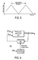
- FIG. 5 illustrates an example output clock modulated for a PC spread spectrum clock application.
- FIG. 6 is a block diagram illustrating one embodiment for a frequency modulator that uses the frequency synthesis techniques of the present invention.
- FIG. 7A is a block diagram illustrating an application for the frequency synthesis techniques of the present invention.
- FIG. 7B is a block diagram illustrating another application for the frequency synthesis techniques of the present invention.
- FIG. 8 is a block diagram illustrating one embodiment for a clock synthesis circuit that employs a pulse density modulator.
- FIG. 9 is a flow diagram illustrating logic for one embodiment of the pulse density modulator.
- FIG. 10 is a block diagram that illustrates mapping a bit number, X, to a three bit number, Y.
- FIG. 11 is a block diagram illustrating one embodiment for a spread spectrum clock generation control circuit.
- FIG. 12 is a graph that illustrates parameters for controlling modulation of the clock frequency.
- FIG. 13 is a schematic diagram illustrating a conventional charge pump loop filter circuit within the frequency synthesizer circuit
- FIG. 14 is a graph illustrating the effect of a phase offset on the control voltage within the frequency synthesizer circuit
- FIG. 15 is a graph illustrating the effect of a phase offset on the conventional charge pump loop filter circuit
- FIG. 16 is a schematic diagram illustrating a switched capacitor charge pump loop filter circuit within the frequency synthesizer circuit, according to one embodiment of the invention.
- FIG. 17 is a graph illustrating the effect of a phase offset on the switched capacitor charge pump loop filter circuit
- FIG. 18 is a block diagram illustrating a Complementary Metal Oxide Semiconductor (“CMOS”) buffer based, switched capacitor adaptive bandwidth phase locked loop circuit, according to one embodiment of the invention
- FIG. 19 is a block diagram illustrating a circuit to scale the charge pump current within the adaptive bandwidth phase locked loop circuit, according to one embodiment of the invention.
- FIG. 20 is a block diagram illustrating a circuit to scale the charge pump current within the adaptive bandwidth phase locked loop circuit, according to an alternate embodiment of the invention.
- FIG. 21 is a block diagram illustrating an inductive-capacitive (“LC”) tank based, switched capacitor adaptive bandwidth phase locked loop circuit, according to one embodiment of the invention.
- LC inductive-capacitive
- a frequency synthesizer includes a phase locked loop architecture that utilizes a phase interpolator in the feedback path.
- the phase locked loop achieves very high frequency resolution while maintaining high loop bandwidth.
- the phase locked loop of the frequency synthesizer is configured as a ring oscillator based spread spectrum phase locked loop. In other embodiments, the phase locked loop is configured as a frequency modulator.
- FIG. 1 is a block diagram illustrating one embodiment for a frequency synthesizer of the present invention.
- a frequency synthesizer circuit 100 employs a phase locked loop circuit 120 .
- Phase locked loop circuit 120 receives, as input, a clock reference (Clk ref ) and a feedback clock (Clk fb ), and generates, as an output, an output clock (Clk out ).
- an interpolator 130 is part of the feedback path of phase locked loop 120 .
- the interpolator 130 introduces a phase delay to the output clock (Clk out ).
- the interpolator 130 introduces a time variable delay to the output clock based on two or more phases of the output clock.
- the output of the interpolator 130 the phase shifted or phase delayed output clock, is referenced as the feedback clock (Clk fb ) in FIG. 1 .
- interpolator 130 may comprise an analog circuit capable of generating continuous phase delays.
- the interpolator 130 comprises a digital circuit that varies the phase of the output clock (Clk out ) in discrete intervals.
- the disclosure sets forth digital circuit embodiments for interpolator 130 ; however, interpolator 130 may be implemented in analog circuits without deviating from the spirit or scope of the invention.
- the interpolator 130 comprises a phase interpolator that generates the feedback clock (Clk fb ) from two reference clocks (e.g., a clock with two different phases).
- the phase of the feedback clock (Clk fb ) is a weighted sum, based on the interpolator control word, of the phases of the two reference clocks.
- Embodiments for implementing a phase interpolator are disclosed in an article entitled “A Semidigital Dual Delay-Locked Loop”, IEEE Journal of Solid State Circuits, Vol. 32, No. 11, November 1997, authors Stefanos Sidiropoulos and Mark A. Horowitz.
- the phase of the output clock may be varied over time by changing the delay of the interpolator in discrete increments. Furthermore, the size of these increments may be varied over time.
- the feedback delay, introduced by interpolator 130 is controlled by an interpolator control word.
- the interpolator control word is a digital word comprising “n” bits.
- an interpolator control circuit 140 controls the phase delay in interpolator 130 by generating the interpolator control word. The interpolator control circuit 140 modulates the value of the “n” bit interpolator control word.
- the “n” bit control word controls the phase delay in interpolator 130 .
- a desired frequency is generated at the output of the phase locked loop (e.g., clock output).
- the phase delay is also slewed over time so as to generate a variable output frequency is generated.
- FIG. 2 is a block diagram illustrating one embodiment of the frequency synthesizer of the present invention.
- the phase locked loop consists of a phase detector circuit 210 , charge pump-loop filter 220 , and voltage controlled oscillator (“VCO”) 230 .
- the phase detector 210 receives a reference clock (Clk ref ) and a feedback clock (Clk fb ) that is generated by the feedback path of the phase locked loop.
- the phase detector circuit 210 generates a voltage value indicative of the phase difference between the input clock signals.
- the phase value accumulates in a charge pump circuit to produce a loop filter response to the phase difference.
- the voltage output from the charge pump-loop filter circuit 220 is used as the input voltage to VCO 230 .
- VCO 230 generates an output frequency, within a specified range, based on the input voltage value.
- interpolator 240 introduces a variable delay in the output clock so as to vary the phase rate-of-change (i.e. phase slew) over time. This variable delay, controlled by interpolator control circuit 250 , ultimately generates a time varying output frequency at the output of the VCO (Clk out ).
- a divider circuit 240 which divides the clock frequency by an integer value, “N”, is also inserted in the phase locked loop feedback path.
- the divider 240 permits generating a high frequency output signal (Clk out ) based on a lower frequency reference clock (Clk ref ).
- the frequency of the VCO 230 output, CLK out may be defined by: F ref *N. If the value of the interpolator control word is continuously incremented by 1, then the frequency of the VCO output differs from F ref *N by a frequency proportional to the resulting phase slew.
- the output frequency for a constant phase slew may be defined as:
- increment range represents the number of phase increments incremented that the interpolator can produce relative to a period of the output clock
- increment interval represents the amount of time an interpolator control word (i.e. a specific phase delay) is applied relative to a cycle of the output clock.
- the interpolator control word may have 8 bits of resolution. This means that the delay through the interpolator may be varied from 0 to 255/256 times the period of the output clock in steps that are 1/256 the period of the output clock.
- interpolator 240 may delay the output clock for any of 256 phases within a VCO output period (i.e., the increment range is equal to 256). For this example, if the interpolator control word is incremented once every four cycles of the VCO clock (i.e., the increment interval is equal to 4 VCO clock cycles), then the output frequency is equal to: F ref *N*(1+1/256*4).
- the interpolator 130 ( FIG. 1 ) or 240 ( FIG. 2 ) is programmed to introduce a variable phase delay during a specified period of time.
- the “increment size” refers to the magnitude in the step size for the phase delay.
- an 8 bit control word may be programmed to one of 256 phase delays.
- the increment size is 1.
- the increment size may be set to any integer value within the range of 256 phase delays. For example, if the increment size is set to “2”, then the phase is slewed using control word values of “0”, “2”, “4”, “6”, etc.
- FIG. 3 is a graph illustrating another embodiment for varying the phase in the interpolator.
- the vertical axis for the graph represents the phase increment size.
- the interpolator control circuit is designed so that the interpolator control word is the accumulated value of phase increments.
- the example of FIG. 3 constantly-changing increment sizes.
- the horizontal axis of FIG. 3 represents time or cycles of the output clock. Specifically, the incremental duration and incremental interval are depicted on the horizontal axis.
- the increment duration refers to the time over which the change in increment value has the same sign.
- the increment size is decreasing. This produces an output clock frequency that is linearly decreasing in value over the increment duration.
- the increment size is increasing. This produces and output clock frequency that is linear increasing in value of the increment duration.
- the example phase modulation shown in FIG. 3 depicts constant increment interval and increment duration, the increment interval and increment duration may be varied to generate any variable profile frequency desired.
- the interpolator control circuit 250 may comprise a logic circuit that comprises multiple accumulators.
- FIG. 4 is a block diagram illustrating one embodiment to generate a time variable output frequency.
- Circuit 400 of FIG. 4 has application for use as a personal computer (PC) spread spectrum clock.
- the circuit 400 generates an interpolator control word that modulates the phase delay so as to form an output frequency modulated in a triangular fashion.
- FIG. 5 illustrates an example output clock modulated for a PC spread spectrum application. The period of the triangular shaped waveform is based on the increment duration used to slew the phase in the interpolator.
- the interpolator control circuit 400 employs accumulate and dump techniques.
- an increment value is accumulated in flip-flop 430 and a phase value is accumulated in flip-flop 470 .
- Values for the increment interval and the increment duration are stored in registers 440 and 450 , respectively.
- a word clock (Clk word ), which provides timing for the interpolator control circuit, is input to registers 440 and 450 to shift the incremental interval and the incremental duration values, respectively.
- the increment interval value is the clock input to flip-flop 430
- the increment duration value is the clock input to flip-flop 460 .
- Increment values are accumulated in flip-flop 430 each increment interval. The increment values are either incremented or decremented.
- the increment values are decremented during the first incremental duration, and incremented during the second increment duration.
- the increment/decrement selection is controlled through the output of flip-flop 460 and multiplexor 420 .
- the size of the increment/decrement is controlled by the increment size value input to summer/subtractor 405 and 410 .
- the increment value is incremented/decremented in summer/subtractor 405 and 410 , and the selected output is input to flip-flop 430 .
- the increment value is input and accumulated in flip-flop 470 .
- the accumulated value in flip-flop(s) 470 represent the phase value.
- the output of flip-flop(s) 470 is the interpolator control word.
- interpolator control circuit 400 of FIG. 4 modulates the output frequency in a triangular waveform, any type of variable frequency output may be generated by selective programming of the increment size, increment interval, and incremental duration parameters without deviating from the spirit or scope of the invention.
- FIG. 6 is a block diagram illustrating one embodiment for a frequency modulator that uses the frequency synthesis techniques of the present invention.
- a circuit 600 includes a phase locked loop circuit 610 and an interpolator 630 inserted in the phase locked loop feedback path.
- interpolator 630 is controlled by modulation control circuit 640 .
- modulation control 640 receives data for modulation.
- modulation circuit 640 may be configured to modulate input digital data in accordance with a frequency shift key (FSK) modulation scheme.
- the modulation control 640 may be configured to generate any frequency based modulation scheme by programming a variable phase delay in the interpolator.
- the modulation control 640 generates a modulation control word for input to interpolator 630 .
- the modulation control word programs the interpolator 630 to produce a time variable delay on the modulated feedback (Mod fb ) signal.
- the modulated output comprises a frequency modulated output.
- FIG. 7A is a block diagram illustrating an application for the frequency synthesis techniques of the present invention.
- This application permits generating a clock frequency offset, a predetermined amount, from a first frequency.
- circuits that employ two frequencies that are not multiples thereof are generated using two different crystals.
- the technique of the present invention permits generating two different frequencies without the use of multipliers and dividers, so as to eliminate the need for two crystals.
- a clock reference (Clock ref ) signal is input to a clock synthesis circuit 710 to generate a clock one (Clock 1 ) signal.
- clock synthesis circuit 710 multiplies the reference clock to convert a low-frequency reference clock to a high-frequency clock.
- the high-frequency clock may be used in optical networking applications that require operation at the SONET line rate of 9.953 Gigabits per second (“Gb/s”) and at the 10 Gb Ethernet line rate of 10.3125 Gb/s.
- the first clock is input to phase locked loop circuit 720 which, along with the interpolator 730 in the feedback path, generates a second clock (Clock 2 ).
- FIG. 7B is a block diagram illustrating another application for the frequency synthesis techniques of the present invention.
- a first clock, Clock 1 is generated in Clock 1 synthesis circuit 740 from a reference clock, Clock ref , similar to the embodiment of FIG. 7A .
- Clock 2 is also generated from the reference clock, Clock ref , and the output of interpolator 760 in phase locked loop circuit 750 .
- This embodiment permits generating two clocks, Clock 1 and Clock 2 , at different frequencies, without requiring a rational number relationship between the clock frequencies. In other words, the relationship between the clock frequencies is not required to be M/N, where M and N are integer values.
- the frequency resolution of the feedback interpolator technique described above is limited by the resolution of the interpolator and the maximum operating frequency of the controller that generates the control word. In some applications, it is desirable to increase the resolution of the rate at which the interpolator control word is changed. However, if the control clock frequency resolution is increased, higher frequency components are introduced into the phase locked loop feedback path. The high frequency components of the control clock are filtered in the low pass filter of the phase locked loop. Accordingly, it is desirable to increase the resolution at which the interpolator control word is changed without filtering the higher frequency components in the phase locked loop low pass filter.
- the resolution may be increased by exploiting the fact that the phase transfer function from the interpolator output to the output of the voltage controlled oscillator (VCO) has a low pass characteristic.
- VCO voltage controlled oscillator
- the dithering may be performed using a ⁇ modulator coupled to the interpolator control circuit.
- a ⁇ modulator maps an X bit value to a Y bit value, wherein Y ⁇ X.
- modulation such as a ⁇ modulator, the frequency resolution of the interpolator is limited only by the amount of quantization noise that passes through the phase locked loop transfer function.
- a ⁇ modulator may be used to effectively increase the resolution of the rate at which the interpolator control word is changed, it typically involves complex hardware implementations.
- a pulse density modulator is utilized to map an X bit value to a Y bit value, wherein Y ⁇ X.
- the pulse density modulator is implemented with simple logic, so as to decrease the complexity of the hardware implementation. In applications that require a variable output frequency, the required rate of the output frequency change is typically slow when compared with the output frequency itself.
- the six bits of information which changes at a frequency of F/8, are mapped to three bits of information that changes at a frequency of F.
- the six bit binary number, 000100 is optimally mapped to the following series of eight three bit numbers: 000, 001, 000, 001, 000, 001, 000, 001.
- the three bit binary series is the best approximation of the original six bit number after the frequency is low pass filtered (i.e., the three bit number series contains less high-frequency components than the original six bit binary number).
- the three bit series create the least amount of quantization noise at the output of the low pass filter because it contains the highest possible frequency components.
- FIG. 8 is a block diagram illustrating one embodiment for a clock synthesis circuit that employs a pulse density modulator. Similar to the embodiment of FIGS. 1 and 2 , a phase locked loop circuit 120 generates a clock output (Clk out ) from a reference clock (Clk ref ) and a feedback clock (Clk fb ). The interpolator 130 generates the feedback clock (Clk fb ) from the clock output (Clk out ). The interpolator 130 receives interpolator control words generated by the interpolator control circuit 820 . For the embodiment of FIG. 8 , a pulse density modulator 810 is coupled to the interpolator control circuit 820 .
- the pulse density modulator 810 generates timing information to dither the interpolator control word.
- the pulse density modulator emulates a Y bit counter by generating a series of X bit numbers that, over an average, are equivalent to the Y bit number.
- FIG. 9 is a flow diagram illustrating logic for one embodiment of the pulse density modulator.
- the algorithm maps a Y bit number to an X bit number such that the average of the X bit number is equivalent to the Y bit number.
- the most significant bit positions of the Y bit number are designated as “X” bits, and the least significant bit positions are designated as “X LSB ” numbers (block 910 , FIG. 9 ).
- FIG. 10 is a block diagram that illustrates mapping a bit number, X, to a three bit number, Y.
- the “X” bits are the three most significant bits (X 5 X 4 X 3 )
- the X LSB bits are the three least significant bits (X 2 X 1 X 0 ) as shown in FIG.
- the following algorithm is illustrated using a counter (with width equal to X LSB running at 8 times the update rate of X) to map the Y bit number to an X bit number.
- the process detects the bit transition from zero to one (blocks 915 and 920 , FIG. 9 ). For example, if the counter increments from “000” to “001”, then the least significant bit position, X 0 , is the detected bit position.
- a “1” hot mask is generated for the detected bit position (block 930 , FIG. 9 ). For the counter transition example above, the hot mask is set to “001.”
- the process generates a bit sequence by reversing the order of the X LSB bits (block 940 , FIG. 9 ). For the above example, this bit sequence is set to “100.”
- a Boolean AND operation is performed between each respective bit of the bit sequence and the mask (block 945 , FIG. 9 ).
- a bitwise Boolean AND operation is performed between 001 and 100 (i.e., 0&1, 0&0, and 0&0).
- the result of the example bitwise Boolean AND operation yields “000.”
- a bit wise Boolean OR operator is executed among the results of the Boolean AND operation (block 950 , FIG. 9 ).
- FIG. 11 is a block diagram illustrating one embodiment for a spread spectrum clock generation control circuit.
- clock generation control circuit 1100 generates an interpolator control word to modulate the frequency of a clock in the form of a saw tooth wave function to drive the clock synthesis circuit that generates the variable frequency output (e.g., the saw tooth wave function output).
- the interpolator control word comprises an eight bit value.
- the control circuit 1100 generates an eight bit interpolator control word, any size or resolution for the interpolator control word may be generated using the pulse density modulator techniques of the present invention.
- a saw generator control circuit 1105 generates data to control phase slew in the clock synthesis circuit.
- Pulse density modulator circuit 1110 is coupled to receive the output from saw generator circuit 1105 .
- pulse density modulator circuit 1110 increases the resolution of the interpolator control word as described above.
- Saw generator circuit 1105 receives, as inputs, the maximum increment range (“SSCMax”), the increment step size (“SSCInc”), the increment interval (“SSCIncIntrv”) and the center of the cycle (“SSCCenter”).
- FIG. 12 is a graph that illustrates parameters for controlling modulation of the clock frequency.
- the horizontal axis of the graph depicts cycles for generating the interpolator control words.
- the increment interval depicted by the variable SSCIncIntv, specifies a duration of time for a single interval.
- the vertical axis of the graph of FIG. 12 depicts increment size.
- a single increment size is depicted with the variable SSCInc.
- the maximum increment range in a cycle is depicted in FIG. 12 by the variable SSCMax.
- saw generator circuit 1105 receives a ck_saw for timing of the circuit.
- the pulse density modulator circuit 1110 receives, for its timing, a wordclk. For this example, which maps six bits of resolution to three bits of resolution, the saw generator clock, ck_saw, has a frequency 1 ⁇ 8 th the frequency of the word clock.
- the pulse density modulator 1110 receives the output of the saw generator 1105 .
- pulse density modulator 1110 generates a three bit output in accordance with the algorithm outlined in the flow diagram of FIG. 9 .
- SAW generator control circuit 1100 permits bypassing the increased resolution output, generated by pulse density modulator 1110 .
- the outputs of saw generator circuit 1105 and pulse density modulator 1110 are input to multiplexer 1120 .
- Multiplexer 1120 permits selection of either the saw generator output or the pulse density modulator output.
- the saw generator and pulse density modulator outputs may be bypassed, through multiplexer 1130 .
- control circuit 1100 operates from the maximum increment cycle variable.
- an accumulator circuit is used in the embodiment of control circuit 1100 .
- a register flip-flop 1170 holds an accumulated value for the interpolator control word, SSCinterp.
- the increment size is either added or subtracted to the accumulated value through summer 1140 or subtractor 1150 based on the portion of the cycle.
- the increment or decrement function is selected through multiplexer 1160 and the control variable, SSCInvert.
- FIG. 13 is a schematic diagram illustrating a conventional charge pump loop filter circuit within the frequency synthesizer circuit 200 .
- the charge pump-loop filter circuit 1300 includes a charge pump device 1310 coupled to a loop filter consisting of a filter resistor 1320 coupled to a capacitor 1330 .
- FIG. 14 is a graph illustrating the effect of a phase offset on the control voltage within the frequency synthesizer circuit. If a conventional charge pump-loop filter circuit 1300 is used within the circuit 200 and a phase offset is present a the PFD circuit 210 then the correction voltage generated at the input of the VCO will be concentrated in a short period of time ⁇ T.
- FIG. 15 is a graph illustrating the effect of the phase offset on the conventional charge pump loop filter circuit. As illustrated in FIG. 15 , ⁇ T is the phase offset between the reference clock signal and the feedback clock signal.
- the frequency synthesis circuit uses a switch capacitor filter in the phase locked loop. Specifically, in order to alleviate any potential disturbances introduced in the control voltage V C output by the charge pump 1310 described in FIG. 13 , a switched capacitor loop filter is coupled to a charge pump.
- FIG. 16 is a schematic diagram illustrating a switched capacitor charge pump loop filter circuit 1600 within the frequency synthesizer circuit, according to one embodiment of the invention.
- the charge pump current, I CP at the charge pump 1310 flows to a capacitor C 1 1610 every reference clock cycle, T REF .
- a buffer 1620 having a gain, g is coupled to the charge pump 1310 to sum up the current I CP with a control voltage accumulated at a capacitor C CP 1630 .
- a zero impedance switch, S 1 , 1640 is further activated once every reference clock cycle, T REF , through an impulse signal to equalize the voltages between the capacitors C 1 1610 and C CP 1640 .
- the output voltage V C drives a voltage control oscillator, such as the VCO 230 described in connection with FIG. 2 .
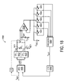
- FIG. 18 is a block diagram illustrating a Complementary Metal Oxide Semiconductor (“CMOS”) buffer based, switched capacitor adaptive bandwidth phase locked loop circuit, according to one embodiment of the invention.
- the phase locked loop circuit 1800 includes two charge pump devices CP 1 1810 , and CP 2 1820 , each coupled to a PFD circuit 1805 and configured to receive an up signal or a down signal, respectively, depending on the values of a reference frequency signal, f REF , and a feedback frequency signal, f OUT .
- Each charge pump, 1810 and 1820 is further coupled to a capacitor C 1 1811 and C 1 1821 , respectively.
- one path containing a charge pump, and its corresponding capacitor such as for example, the path including charge pump 1810 and capacitor 1811 , is active and generates a loop integral control voltage, V INT , while the other path, such as, for example, the path including charge pump 1820 and its corresponding capacitor 1821 , is equalizing.
- the voltage control oscillator (“VCO”) of the phase locked loop circuit 1800 is controlled using a three-input differential amplifier module 1830 , that buffers the output voltages at the charge pumps 1810 , 1820 and outputs a VCO control voltage, V C .
- the amplifier module 1830 is further coupled to a predetermined number of inverters, such as, for example inverters 1841 , 1842 , 1843 , 1844 and 1845 coupled in series.
- the VCO may also be implemented as a cascade of two-input differential amplifiers.
- the signal output from each inverter is input to interpolator 1850 .
- the clock feedback path further consists of a programmable 1/N divider circuit 1860 .
- the current I CP of the charge pumps ( 1810 or 1820 ) may be derived from the VCO control voltage, V C , and may be scaled inversely proportional to the phase locked loop frequency multiplication factor, N. This enables the loop circuit 1800 to achieve close to optimal characteristics.
- the loop damping factor, ⁇ only depends on a ratio of capacitors and the loop bandwidth, ⁇ B , and the natural frequency are both independent of process variations and both scale with the reference frequency, f REF .
- FIG. 19 is a block diagram illustrating a circuit to scale the charge pump current within the adaptive bandwidth phase locked loop circuit, according to one embodiment of the invention.
- the charge pump 310 is biased through a digital-to-analog converter module (“DAC”) 1910 .
- the DAC 1910 receives, as inputs, the control voltage, V C , and the frequency multiplication factor N, and outputs a current that is inversely proportional to the N factor. This enables the scaling of the charge pump current I CP to be inversely proportional to the PLL frequency multiplication factor N, such that: I CP ⁇ ( V C ⁇ V T ) 2 ⁇ 1/ N.
- FIG. 20 is a block diagram illustrating a circuit to bias the charge pump current within the adaptive bandwidth phase locked loop circuit, according to an alternate embodiment of the invention.
- the charge pump 310 is biased using a switched capacitor circuit, which also enables scaling of the charge pump current I CP inversely proportional to the PLL frequency multiplication factor, N.
- F REF ⁇ (R ON ⁇ C LD ⁇ N) ⁇ 1 and R ON ⁇ 1/ ⁇ (V C ⁇ V T ), which results in I CP ⁇ ( V C ⁇ V T ) 2 ⁇ 1/ N.
- FIG. 21 is a block diagram illustrating an inductive-capacitive (“LC”) tank based, switched capacitor adaptive bandwidth phase locked loop circuit, according to one embodiment of the invention.
- the phase locked loop circuit 2100 includes two charge pump devices CP 1 2110 , and CP 2 2120 .
- Each charge pump device is coupled to a PFD circuit 2105 and configured to receive an up signal or a down signal, respectively, depending on the values of a reference frequency signal, f REF , and a feedback frequency signal, f OUT .
- Each charge pump 2110 , 2120 is further coupled to a capacitor C 1 2111 and C 1 2121 , respectively.
- one path containing a charge pump and its corresponding capacitor such as for example, the path including charge pump 2110 and capacitor 2111 , is active and generates a loop integral control voltage V INT , while the other path, such as, for example, the path including charge pump 2120 and its corresponding capacitor 2121 , is equalizing.
- the voltage control oscillator (“VCO”) of the phase locked loop circuit 1100 is implemented as a resonant tank containing an inductor L 2130 coupled to a capacitor C T 2140 , and three varactors C V 2150 coupled in parallel.
- the three varactors C V 2150 average the three output voltage signals at the output of the two charge pumps 2110 and 2120 .
- the base bias current, I CP , of the two charge pumps 2110 and 2120 are set, by way of example, by using a band-gap circuit that varies inversely proportional with the phase locked loop frequency multiplication factor, N.
Abstract
Description
Fref*N.
If the value of the interpolator control word is continuously incremented by 1, then the frequency of the VCO output differs from Fref*N by a frequency proportional to the resulting phase slew. The output frequency for a constant phase slew may be defined as:
wherein, “increment range” represents the number of phase increments incremented that the interpolator can produce relative to a period of the output clock, and “increment interval” represents the amount of time an interpolator control word (i.e. a specific phase delay) is applied relative to a cycle of the output clock. For example, the interpolator control word may have 8 bits of resolution. This means that the delay through the interpolator may be varied from 0 to 255/256 times the period of the output clock in steps that are 1/256 the period of the output clock. Thus, for this example,
Fref*N*(1+1/256*4).
V C(T)=(∫T O I CP(τ)dτ/C CP)+I CP(T)·R
H(s)=N·(1+2·ζ·s/ω B/1+2·ζ·s/ω B+(s/ω B)2)
wherein, the loop damping factor ζ and the loop bandwidth ωB are given by:
ζ=0.5·R·√I CP ·K VCO ·C CP /N and ωB=2·ζ/(R·C CP)
then for
R≈T REF /C 1=1/(2·π·f REF ·C 1),
R ON≈1/β(V C −V T); (1)
wherein, RON denotes the charging resistance of the inverter used in the VCO,
T≈R ON ·C LD ·N; (2)
wherein, CLD·denotes the capacitive load seen by the inverters in the VCO,
K VCO ≈β/C LD; and (3)
I CP≈β(V C −V T)2·1/N; (4)
The circuit operation, as characterized in equation (4), results in regulation of process, temperature and voltage variations for different loop bandwidths.
ζ≈√(C LD C CP)/C 1 2
and the loop bandwidth, ωB, may be calculated as
ωB=2·/(R·C CP)≈f REF·(2π)2ζC 1 /C CP.
Thus, the loop damping factor, ζ, only depends on a ratio of capacitors and the loop bandwidth, ωB, and the natural frequency are both independent of process variations and both scale with the reference frequency, fREF.
I CP≈β(V C −V T)2·1/N.
I CP ≈C X(V C −V T)·F REF.
where FREF≈(RON·CLD·N)−1 and RON≈1/β(VC−VT), which results in
I CP≈β(V C −V T)2·1/N.
ζ=0.5·R·√I CP ·K VCO ·C CP /N
and R≈T REF /C 1 and T REF =NT VCO ≈N√L·C T
then, the loop damping factor may be calculated with the following formula:
ζ≈√(I CP ·K VCO ·L·C T ·C CP)/C 1 2
and the loop bandwidth may be calculated as:
ωB=2·ζ/(R·C CP)≈ωREF·2ζC 1 /C CP.
Claims (18)
Priority Applications (6)
| Application Number | Priority Date | Filing Date | Title |
|---|---|---|---|
| US11/296,786 US7432750B1 (en) | 2005-12-07 | 2005-12-07 | Methods and apparatus for frequency synthesis with feedback interpolation |
| US11/321,412 US7323916B1 (en) | 2005-12-07 | 2005-12-29 | Methods and apparatus for generating multiple clocks using feedback interpolation |
| US11/861,690 US7436229B2 (en) | 2005-12-07 | 2007-09-26 | Methods and apparatus for minimizing jitter in a clock synthesis circuit that uses feedback interpolation |
| US11/938,164 US7443215B1 (en) | 2005-12-07 | 2007-11-09 | Methods and apparatus to increase the resolution of a clock synthesis circuit that uses feedback interpolation |
| US12/130,732 US8433018B2 (en) | 2005-12-07 | 2008-05-30 | Methods and apparatus for frequency synthesis with feedback interpolation |
| US12/185,750 US8667038B1 (en) | 2005-12-07 | 2008-08-04 | Methods and apparatus to increase the resolution of a clock synthesis circuit that uses feedback interpolation |
Applications Claiming Priority (1)
| Application Number | Priority Date | Filing Date | Title |
|---|---|---|---|
| US11/296,786 US7432750B1 (en) | 2005-12-07 | 2005-12-07 | Methods and apparatus for frequency synthesis with feedback interpolation |
Related Child Applications (4)
| Application Number | Title | Priority Date | Filing Date |
|---|---|---|---|
| US11/321,412 Continuation US7323916B1 (en) | 2005-12-07 | 2005-12-29 | Methods and apparatus for generating multiple clocks using feedback interpolation |
| US11/861,690 Continuation US7436229B2 (en) | 2005-12-07 | 2007-09-26 | Methods and apparatus for minimizing jitter in a clock synthesis circuit that uses feedback interpolation |
| US11/938,164 Continuation US7443215B1 (en) | 2005-12-07 | 2007-11-09 | Methods and apparatus to increase the resolution of a clock synthesis circuit that uses feedback interpolation |
| US12/130,732 Continuation US8433018B2 (en) | 2005-12-07 | 2008-05-30 | Methods and apparatus for frequency synthesis with feedback interpolation |
Publications (1)
| Publication Number | Publication Date |
|---|---|
| US7432750B1 true US7432750B1 (en) | 2008-10-07 |
Family
ID=38973899
Family Applications (6)
| Application Number | Title | Priority Date | Filing Date |
|---|---|---|---|
| US11/296,786 Expired - Fee Related US7432750B1 (en) | 2005-12-07 | 2005-12-07 | Methods and apparatus for frequency synthesis with feedback interpolation |
| US11/321,412 Active US7323916B1 (en) | 2005-12-07 | 2005-12-29 | Methods and apparatus for generating multiple clocks using feedback interpolation |
| US11/861,690 Expired - Fee Related US7436229B2 (en) | 2005-12-07 | 2007-09-26 | Methods and apparatus for minimizing jitter in a clock synthesis circuit that uses feedback interpolation |
| US11/938,164 Expired - Fee Related US7443215B1 (en) | 2005-12-07 | 2007-11-09 | Methods and apparatus to increase the resolution of a clock synthesis circuit that uses feedback interpolation |
| US12/130,732 Expired - Fee Related US8433018B2 (en) | 2005-12-07 | 2008-05-30 | Methods and apparatus for frequency synthesis with feedback interpolation |
| US12/185,750 Expired - Fee Related US8667038B1 (en) | 2005-12-07 | 2008-08-04 | Methods and apparatus to increase the resolution of a clock synthesis circuit that uses feedback interpolation |
Family Applications After (5)
| Application Number | Title | Priority Date | Filing Date |
|---|---|---|---|
| US11/321,412 Active US7323916B1 (en) | 2005-12-07 | 2005-12-29 | Methods and apparatus for generating multiple clocks using feedback interpolation |
| US11/861,690 Expired - Fee Related US7436229B2 (en) | 2005-12-07 | 2007-09-26 | Methods and apparatus for minimizing jitter in a clock synthesis circuit that uses feedback interpolation |
| US11/938,164 Expired - Fee Related US7443215B1 (en) | 2005-12-07 | 2007-11-09 | Methods and apparatus to increase the resolution of a clock synthesis circuit that uses feedback interpolation |
| US12/130,732 Expired - Fee Related US8433018B2 (en) | 2005-12-07 | 2008-05-30 | Methods and apparatus for frequency synthesis with feedback interpolation |
| US12/185,750 Expired - Fee Related US8667038B1 (en) | 2005-12-07 | 2008-08-04 | Methods and apparatus to increase the resolution of a clock synthesis circuit that uses feedback interpolation |
Country Status (1)
| Country | Link |
|---|---|
| US (6) | US7432750B1 (en) |
Cited By (13)
| Publication number | Priority date | Publication date | Assignee | Title |
|---|---|---|---|---|
| US20080260071A1 (en) * | 2005-12-07 | 2008-10-23 | Stefanos Sidiropoulos | Methods and Apparatus for Frequency Synthesis with Feedback Interpolation |
| US20100007390A1 (en) * | 2008-07-10 | 2010-01-14 | Wen-Chung Yeh | Clock generating circuit, power converting system, and related method with spread spectrum for EMI reduction |
| US7733151B1 (en) * | 2008-12-08 | 2010-06-08 | Texas Instruments Incorporated | Operating clock generation system and method for audio applications |
| US20110228860A1 (en) * | 2010-03-19 | 2011-09-22 | Marc Loinaz | Multi-Value Logic Signaling in Multi-Functional Circuits |
| US20110228889A1 (en) * | 2010-03-19 | 2011-09-22 | Dean Liu | Repeater Architecture with Single Clock Multiplier Unit |
| US20110231692A1 (en) * | 2010-03-19 | 2011-09-22 | Marc Loinaz | Programmable Drive Strength in Memory Signaling |
| US8102936B2 (en) | 2002-06-21 | 2012-01-24 | Netlogic Microsystems, Inc. | Methods and apparatus for clock and data recovery using transmission lines |
| CN101728939B (en) * | 2008-10-16 | 2012-07-11 | 通嘉科技股份有限公司 | Periodic signal generating circuit, power conversion system and method using circuit |
| US20130093478A1 (en) * | 2011-10-13 | 2013-04-18 | National Semiconductor Corporation | Differentiator based spread spectrum modulator |
| US8494377B1 (en) | 2010-06-30 | 2013-07-23 | Netlogic Microsystems, Inc. | Systems, circuits and methods for conditioning signals for transmission on a physical medium |
| US8537949B1 (en) | 2010-06-30 | 2013-09-17 | Netlogic Microsystems, Inc. | Systems, circuits and methods for filtering signals to compensate for channel effects |
| US9379881B1 (en) * | 2015-03-18 | 2016-06-28 | SK Hynix Inc. | Phase interpolator circuit, clock data recovery circuit including the same, and phase interpolation method |
| US11323131B2 (en) | 2019-11-06 | 2022-05-03 | Stmicroelectronics International N.V. | Delay-based spread spectrum clock generator circuit |
Families Citing this family (103)
| Publication number | Priority date | Publication date | Assignee | Title |
|---|---|---|---|---|
| US7181180B1 (en) * | 2003-05-15 | 2007-02-20 | Marvell International Ltd. | Sigma delta modulated phase lock loop with phase interpolation |
| JPWO2006033203A1 (en) * | 2004-09-21 | 2008-05-15 | 株式会社アドバンテスト | Delay lock loop circuit, phase lock loop circuit, timing generator, semiconductor test apparatus, and semiconductor integrated circuit |
| US7532697B1 (en) | 2005-01-27 | 2009-05-12 | Net Logic Microsystems, Inc. | Methods and apparatus for clock and data recovery using a single source |
| US7961059B1 (en) | 2005-06-30 | 2011-06-14 | Cypress Semiconductor Corporation | Phase lock loop control system and method with non-consecutive feedback divide values |
| US7813411B1 (en) | 2005-06-30 | 2010-10-12 | Cypress Semiconductor Corporation | Spread spectrum frequency synthesizer with high order accumulation for frequency profile generation |
| US7912109B1 (en) | 2005-06-30 | 2011-03-22 | Cypress Semiconductor Corporation | Spread spectrum frequency synthesizer with first order accumulation for frequency profile generation |
| US8174326B1 (en) | 2005-06-30 | 2012-05-08 | Cypress Semiconductor Corporation | Phase lock loop control error selection system and method |
| US7948327B1 (en) | 2005-06-30 | 2011-05-24 | Cypress Semiconductor Corporation | Simplified phase lock loop control model system and method |
| US8072277B1 (en) * | 2005-06-30 | 2011-12-06 | Cypress Semiconductor Corporation | Spread spectrum frequency synthesizer |
| US7932787B1 (en) | 2005-06-30 | 2011-04-26 | Cypress Semiconductor Corporation | Phase lock loop control system and method |
| US7741918B1 (en) | 2005-06-30 | 2010-06-22 | Cypress Semiconductor Corporation | System and method for an enhanced noise shaping for spread spectrum modulation |
| US7701297B1 (en) | 2005-06-30 | 2010-04-20 | Cypress Semiconductor Corporation | Spread spectrum frequency synthesizer with improved frequency shape by adjusting the length of a standard curve used for spread spectrum modulation |
| US7706767B2 (en) * | 2006-03-28 | 2010-04-27 | Qualcomm, Incorporated | Dual path loop filter for phase lock loop |
| DE102006024960B4 (en) * | 2006-05-29 | 2013-01-31 | Qimonda Ag | Signal delay loop and method for latching a signal delay loop |
| US7545188B1 (en) * | 2006-08-04 | 2009-06-09 | Integrated Device Technology, Inc | Multiphase clock generator |
| US7551011B2 (en) * | 2006-08-10 | 2009-06-23 | Ameritherm, Inc. | Constant phase angle control for frequency agile power switching systems |
| US8831064B1 (en) * | 2007-06-13 | 2014-09-09 | Xilinx, Inc. | Method of and circuit for generating a spread spectrum clock signal |
| US7728636B2 (en) * | 2007-08-14 | 2010-06-01 | Qimonda Ag | Clock signal synchronizing device with inherent duty-cycle correction capability |
| US8253454B2 (en) * | 2007-12-21 | 2012-08-28 | Realtek Semiconductor Corp. | Phase lock loop with phase interpolation by reference clock and method for the same |
| US7642822B2 (en) * | 2008-04-03 | 2010-01-05 | Tektronix, Inc. | Analog phase-locked loop |
| US7929237B2 (en) * | 2008-06-27 | 2011-04-19 | Agere Systems Inc. | Modulated disk lock clock and methods for using such |
| US20100008409A1 (en) * | 2008-07-09 | 2010-01-14 | International Business Machines Corporation | Method for clock jitter stress margining of high speed interfaces |
| US8300754B2 (en) * | 2008-07-29 | 2012-10-30 | Fujitsu Limited | Clock and data recovery with a data aligner |
| US8718217B2 (en) * | 2008-07-29 | 2014-05-06 | Fujitsu Limited | Clock and data recovery (CDR) using phase interpolation |
| US8300753B2 (en) * | 2008-07-29 | 2012-10-30 | Fujitsu Limited | Triple loop clock and data recovery (CDR) |
| US8411782B2 (en) * | 2008-07-29 | 2013-04-02 | Fujitsu Limited | Parallel generation and matching of a deskew channel |
| US8138798B2 (en) * | 2008-07-29 | 2012-03-20 | Fujitsu Limited | Symmetric phase detector |
| JP4562787B2 (en) * | 2008-07-30 | 2010-10-13 | ルネサスエレクトロニクス株式会社 | PLL circuit |
| KR101566417B1 (en) * | 2008-08-29 | 2015-11-05 | 삼성전자주식회사 | voltage controlled oscillator PLL circuit clock generator and HDMI TX PHY |
| US8949701B2 (en) | 2008-09-23 | 2015-02-03 | Agere Systems Inc. | Systems and methods for low latency media defect detection |
| JP2010135956A (en) * | 2008-12-03 | 2010-06-17 | Renesas Electronics Corp | Pll circuit and method of controlling the same |
| US8320770B2 (en) * | 2009-03-20 | 2012-11-27 | Fujitsu Limited | Clock and data recovery for differential quadrature phase shift keying |
| JP5326911B2 (en) * | 2009-07-30 | 2013-10-30 | 株式会社リコー | Spread spectrum clock generator, circuit device, image reading device, image forming device, and spread spectrum clock generation method |
| US7994829B2 (en) * | 2009-10-16 | 2011-08-09 | Realtek Semiconductor Corp. | Fast lock-in all-digital phase-locked loop with extended tracking range |
| US8842767B2 (en) * | 2009-11-04 | 2014-09-23 | Broadcom Corporation | System and method for un-interrupted operation of communications during interference |
| US9002488B2 (en) * | 2010-02-22 | 2015-04-07 | Cypress Semiconductor Corporation | Clock synthesis systems, circuits and methods |
| US8217692B2 (en) * | 2010-03-03 | 2012-07-10 | King Fahd University Of Petroleum And Minerals | Frequency synthesizer |
| US8566381B2 (en) | 2010-08-05 | 2013-10-22 | Lsi Corporation | Systems and methods for sequence detection in data processing |
| US8237597B2 (en) | 2010-09-21 | 2012-08-07 | Lsi Corporation | Systems and methods for semi-independent loop processing |
| US8566378B2 (en) | 2010-09-30 | 2013-10-22 | Lsi Corporation | Systems and methods for retry sync mark detection |
| US8614858B2 (en) | 2010-11-15 | 2013-12-24 | Lsi Corporation | Systems and methods for sync mark detection metric computation |
| US8526131B2 (en) | 2010-11-29 | 2013-09-03 | Lsi Corporation | Systems and methods for signal polarity determination |
| US8498072B2 (en) | 2010-11-29 | 2013-07-30 | Lsi Corporation | Systems and methods for spiral waveform detection |
| US8411385B2 (en) | 2010-12-20 | 2013-04-02 | Lsi Corporation | Systems and methods for improved timing recovery |
| DE102010063800A1 (en) * | 2010-12-21 | 2012-06-21 | Endress + Hauser Gmbh + Co. Kg | Diplexer for homodyne FMCW radar |
| US8325433B2 (en) | 2011-01-19 | 2012-12-04 | Lsi Corporation | Systems and methods for reduced format data processing |
| US8261171B2 (en) | 2011-01-27 | 2012-09-04 | Lsi Corporation | Systems and methods for diversity combined data detection |
| US8749908B2 (en) | 2011-03-17 | 2014-06-10 | Lsi Corporation | Systems and methods for sync mark detection |
| US8666013B1 (en) * | 2011-03-22 | 2014-03-04 | Altera Corporation | Techniques for clock data recovery |
| US8565047B2 (en) | 2011-04-28 | 2013-10-22 | Lsi Corporation | Systems and methods for data write loopback based timing control |
| US8665544B2 (en) | 2011-05-03 | 2014-03-04 | Lsi Corporation | Systems and methods for servo data detection |
| US8874410B2 (en) | 2011-05-23 | 2014-10-28 | Lsi Corporation | Systems and methods for pattern detection |
| US9331878B2 (en) * | 2011-06-14 | 2016-05-03 | Agency For Science, Technology And Research | Frequency shift keying transmitter |
| US8498071B2 (en) | 2011-06-30 | 2013-07-30 | Lsi Corporation | Systems and methods for inter-track alignment |
| US8669891B2 (en) | 2011-07-19 | 2014-03-11 | Lsi Corporation | Systems and methods for ADC based timing and gain control |
| US8780476B2 (en) | 2011-09-23 | 2014-07-15 | Lsi Corporation | Systems and methods for controlled wedge spacing in a storage device |
| US8773811B2 (en) | 2011-12-12 | 2014-07-08 | Lsi Corporation | Systems and methods for zone servo timing gain recovery |
| US8975975B2 (en) * | 2012-03-30 | 2015-03-10 | Intel Corporation | Spread spectrum clocking method for wireless mobile platforms |
| US9094028B2 (en) | 2012-04-11 | 2015-07-28 | Rambus Inc. | Wide range frequency synthesizer with quadrature generation and spur cancellation |
| US8681444B2 (en) | 2012-06-07 | 2014-03-25 | Lsi Corporation | Multi-zone servo processor |
| US8625216B2 (en) | 2012-06-07 | 2014-01-07 | Lsi Corporation | Servo zone detector |
| US8564897B1 (en) | 2012-06-21 | 2013-10-22 | Lsi Corporation | Systems and methods for enhanced sync mark detection |
| US9019641B2 (en) | 2012-12-13 | 2015-04-28 | Lsi Corporation | Systems and methods for adaptive threshold pattern detection |
| US9053217B2 (en) | 2013-02-17 | 2015-06-09 | Lsi Corporation | Ratio-adjustable sync mark detection system |
| US9099995B2 (en) * | 2013-03-14 | 2015-08-04 | Qualcomm Incorporated | Ring oscillator circuit and method |
| US9196297B2 (en) | 2013-03-14 | 2015-11-24 | Avago Technologies General Ip (Singapore) Pte. Ltd. | Systems and methods for enhanced sync mark mis-detection protection |
| US9275655B2 (en) | 2013-06-11 | 2016-03-01 | Avago Technologies General Ip (Singapore) Pte. Ltd. | Timing error detector with diversity loop detector decision feedback |
| US10152999B2 (en) | 2013-07-03 | 2018-12-11 | Avago Technologies International Sales Pte. Limited | Systems and methods for correlation based data alignment |
| US9129650B2 (en) | 2013-07-25 | 2015-09-08 | Avago Technologies General Ip (Singapore) Pte. Ltd. | Array-reader based magnetic recording systems with frequency division multiplexing |
| TWI512714B (en) * | 2013-08-19 | 2015-12-11 | Sitronix Technology Corp | A power supply circuit of a display device |
| US9129646B2 (en) | 2013-09-07 | 2015-09-08 | Avago Technologies General Ip (Singapore) Pte. Ltd. | Array-reader based magnetic recording systems with mixed synchronization |
| US9323625B2 (en) | 2013-11-12 | 2016-04-26 | Avago Technologies General Ip (Singapore) Pte. Ltd. | Systems and methods for lost synchronization data set reprocessing |
| US9495285B2 (en) | 2014-09-16 | 2016-11-15 | Integrated Device Technology, Inc. | Initiating operation of a timing device using a read only memory (ROM) or a one time programmable non volatile memory (OTP NVM) |
| US9224420B1 (en) | 2014-10-02 | 2015-12-29 | Avago Technologies General Ip (Singapore) Pte. Ltd. | Syncmark detection failure recovery system |
| US9584107B2 (en) | 2014-11-26 | 2017-02-28 | Taiwan Semiconductor Manufacturing Company, Ltd. | Delay line circuit |
| US9553570B1 (en) | 2014-12-10 | 2017-01-24 | Integrated Device Technology, Inc. | Crystal-less jitter attenuator |
| JP6404114B2 (en) * | 2014-12-24 | 2018-10-10 | ラピスセミコンダクタ株式会社 | Frequency modulation circuit and semiconductor device |
| US9369139B1 (en) | 2015-02-14 | 2016-06-14 | Integrated Device Technology, Inc. | Fractional reference-injection PLL |
| US9336896B1 (en) | 2015-03-23 | 2016-05-10 | Integrated Device Technology, Inc. | System and method for voltage regulation of one-time-programmable (OTP) memory programming voltage |
| US9455045B1 (en) | 2015-04-20 | 2016-09-27 | Integrated Device Technology, Inc. | Controlling operation of a timing device using an OTP NVM to store timing device configurations in a RAM |
| KR102376738B1 (en) | 2015-06-17 | 2022-03-23 | 한국전자통신연구원 | Phase locked loop for reducing fractional spur noise |
| US9362928B1 (en) | 2015-07-08 | 2016-06-07 | Integrated Device Technology, Inc. | Low-spurious fractional N-frequency divider and method of use |
| US9954516B1 (en) | 2015-08-19 | 2018-04-24 | Integrated Device Technology, Inc. | Timing device having multi-purpose pin with proactive function |
| US9590637B1 (en) | 2015-08-28 | 2017-03-07 | Integrated Device Technology, Inc. | High-speed programmable frequency divider with 50% output duty cycle |
| US9847869B1 (en) | 2015-10-23 | 2017-12-19 | Integrated Device Technology, Inc. | Frequency synthesizer with microcode control |
| US9614508B1 (en) | 2015-12-03 | 2017-04-04 | Integrated Device Technology, Inc. | System and method for deskewing output clock signals |
| KR102418966B1 (en) | 2016-01-11 | 2022-07-11 | 한국전자통신연구원 | Digital phase locked loop and driving method thereof |
| US10075284B1 (en) | 2016-01-21 | 2018-09-11 | Integrated Device Technology, Inc. | Pulse width modulation (PWM) to align clocks across multiple separated cards within a communication system |
| US9852039B1 (en) | 2016-02-03 | 2017-12-26 | Integrated Device Technology, Inc | Phase locked loop (PLL) timing device evaluation system and method for evaluating PLL timing devices |
| US9859901B1 (en) | 2016-03-08 | 2018-01-02 | Integrated Device Technology, Inc. | Buffer with programmable input/output phase relationship |
| US9692394B1 (en) | 2016-03-25 | 2017-06-27 | Integrated Device Technology, Inc. | Programmable low power high-speed current steering logic (LPHCSL) driver and method of use |
| US9698787B1 (en) | 2016-03-28 | 2017-07-04 | Integrated Device Technology, Inc. | Integrated low voltage differential signaling (LVDS) and high-speed current steering logic (HCSL) circuit and method of use |
| US9581973B1 (en) | 2016-03-29 | 2017-02-28 | Integrated Device Technology, Inc. | Dual mode clock using a common resonator and associated method of use |
| US9954541B1 (en) | 2016-03-29 | 2018-04-24 | Integrated Device Technology, Inc. | Bulk acoustic wave resonator based fractional frequency synthesizer and method of use |
| US9654121B1 (en) | 2016-06-01 | 2017-05-16 | Integrated Device Technology, Inc. | Calibration method and apparatus for phase locked loop circuit |
| RU2635278C1 (en) * | 2016-10-17 | 2017-11-09 | Федеральное государственное бюджетное образовательное учреждение высшего образования "Поволжский государственный технологический университет" | Digital frequency synthesizer with high linearity of law of frequency variation |
| KR20180092512A (en) * | 2017-02-09 | 2018-08-20 | 에스케이하이닉스 주식회사 | Internal clock generation circuit |
| WO2018160569A1 (en) | 2017-03-01 | 2018-09-07 | Analog Devices Global Unlimited Company | Feedforward phase noise compensation |
| CN109039312B (en) * | 2018-08-01 | 2020-03-17 | 电子科技大学 | Hybrid digital pulse width modulator with delay chain optimization function |
| RU2718461C1 (en) * | 2019-09-12 | 2020-04-08 | Федеральное государственное бюджетное образовательное учреждение высшего образования "Поволжский государственный технологический университет" | Digital computing synthesizer of frequency-modulated signals |
| US11070214B1 (en) * | 2020-10-14 | 2021-07-20 | Mellanox Technologies Denmark Aps | Test circuit for a digital phase-locked loop |
| US11165431B1 (en) * | 2020-12-09 | 2021-11-02 | Analog Devices, Inc. | Techniques for measuring slew rate in current integrating phase interpolator |
| KR20220091880A (en) * | 2020-12-24 | 2022-07-01 | 삼성전자주식회사 | Phase interpolation based clock data recovery circuit and communication device including the same |
Citations (10)
| Publication number | Priority date | Publication date | Assignee | Title |
|---|---|---|---|---|
| US5124670A (en) * | 1989-03-31 | 1992-06-23 | Lawton Rodney J | Frequency synthesizers with fractional division |
| US6125157A (en) * | 1997-02-06 | 2000-09-26 | Rambus, Inc. | Delay-locked loop circuitry for clock delay adjustment |
| US6285726B1 (en) * | 1998-05-18 | 2001-09-04 | National Semiconductor Corporation | 10/100 mb clock recovery architecture for switches, repeaters and multi-physical layer ports |
| US6570946B1 (en) * | 1999-11-03 | 2003-05-27 | Ericsson, Inc. | One-hot decoded phase shift prescaler |
| US20030161430A1 (en) * | 2002-02-26 | 2003-08-28 | Fujitsu Limited | Clock recovery circuitry |
| US6650157B2 (en) * | 2002-01-11 | 2003-11-18 | Sun Microsystems, Inc. | Using a push/pull buffer to improve delay locked loop performance |
| US6674824B1 (en) * | 1998-08-18 | 2004-01-06 | National Science Council | Method and circuitry for controlling a phase-locked loop by analog and digital signals |
| US7088534B2 (en) * | 2003-04-08 | 2006-08-08 | Marvell International Ltd. | Disk synchronous write |
| US7162002B2 (en) * | 2002-03-01 | 2007-01-09 | Broadcom Corporation | Phase-interpolator based PLL frequency synthesizer |
| US7161443B2 (en) * | 2004-09-30 | 2007-01-09 | Broadcom Corporation | Temperature compensated crystal oscillator |
Family Cites Families (53)
| Publication number | Priority date | Publication date | Assignee | Title |
|---|---|---|---|---|
| FR2034371A1 (en) | 1969-03-21 | 1970-12-11 | Lignes Telegraph Telephon | |
| JPS5292413A (en) | 1976-01-30 | 1977-08-03 | Toshiba Corp | Data transfer system |
| US4021757A (en) * | 1976-04-08 | 1977-05-03 | Rca Corporation | Phase lock-loop modulator using an arithmetic synthesizer |
| US4314212A (en) | 1979-05-31 | 1982-02-02 | Q-Dot, Inc. | Transient data recorder systems |
| US4586010A (en) | 1982-09-30 | 1986-04-29 | Q-Dot, Inc. | Charge splitting sampler systems |
| US4507629A (en) | 1983-03-01 | 1985-03-26 | Frank Gilbert H | Microwave phase shifter |
| US4621242A (en) | 1984-03-19 | 1986-11-04 | The Perkin-Elmer Corporation | R.F. impedance match control system |
| US5471162A (en) | 1992-09-08 | 1995-11-28 | The Regents Of The University Of California | High speed transient sampler |
| JP3549003B2 (en) | 1993-08-31 | 2004-08-04 | 株式会社日立製作所 | Information sending device and information sending / receiving system |
| US5488627A (en) * | 1993-11-29 | 1996-01-30 | Lexmark International, Inc. | Spread spectrum clock generator and associated method |
| DE69533913T2 (en) * | 1994-05-26 | 2005-05-25 | Matsushita Electric Industrial Co., Ltd., Kadoma | frequency synthesizer |
| US5712882A (en) | 1996-01-03 | 1998-01-27 | Credence Systems Corporation | Signal distribution system |
| US5774084A (en) | 1996-04-03 | 1998-06-30 | Sicom, Inc. | Method and apparatus for translating digital data into an analog signal |
| US5864250A (en) | 1996-05-21 | 1999-01-26 | Advanced Communications Devices Corporation | Non-servo clock and data recovery circuit and method |
| US6317008B1 (en) * | 1998-01-26 | 2001-11-13 | Agere Systems Guardian Corp. | Clock recovery using an injection tuned resonant circuit |
| US6226332B1 (en) | 1998-11-13 | 2001-05-01 | Broadcom Corporation | Multi-pair transceiver decoder system with low computation slicer |
| US6181209B1 (en) * | 1998-12-04 | 2001-01-30 | Winbond Electronics Corp. | All-digital frequency following system |
| US6281822B1 (en) | 1999-05-28 | 2001-08-28 | Dot Wireless, Inc. | Pulse density modulator with improved pulse distribution |
| US6242990B1 (en) | 1999-06-16 | 2001-06-05 | Tlc Precision Wafer Technology, Inc. | Quadrature phase shift keyed/bi-phase shift keyed modulator |
| US6961546B1 (en) | 1999-10-21 | 2005-11-01 | Broadcom Corporation | Adaptive radio transceiver with offset PLL with subsampling mixers |
| US6631144B1 (en) | 1999-12-21 | 2003-10-07 | Intel Corporation | Multi-rate transponder system and chip set |
| US6510526B1 (en) | 1999-12-23 | 2003-01-21 | Intel Corporation | Differential clocking for digital platforms |
| GB2362045B (en) * | 2000-02-23 | 2004-05-05 | Phoenix Vlsi Consultants Ltd | Analogue-Controlled phase interpolator |
| US7167517B2 (en) | 2000-05-22 | 2007-01-23 | The Board Of Trustees Of The Leland Stanford Junior University | Analog N-tap FIR receiver equalizer |
| US6901126B1 (en) * | 2000-06-30 | 2005-05-31 | Texas Instruments Incorporated | Time division multiplex data recovery system using close loop phase and delay locked loop |
| SG96571A1 (en) | 2000-09-27 | 2003-06-16 | Oki Techno Ct Singapore Pte | Method and device for pulse density modulation |
| US6565157B2 (en) | 2001-02-23 | 2003-05-20 | Shelby Williams Industries, Inc. | Molded foam spring seat |
| JP4587620B2 (en) * | 2001-09-10 | 2010-11-24 | ルネサスエレクトロニクス株式会社 | Clock control method, frequency dividing circuit and PLL circuit |
| US7092474B2 (en) | 2001-09-18 | 2006-08-15 | Broadcom Corporation | Linear phase detector for high-speed clock and data recovery |
| US6566900B2 (en) | 2001-09-27 | 2003-05-20 | Sun Microsystems, Inc. | Integrated on-chip process, temperature, and voltage sensor module |
| US20030081709A1 (en) | 2001-10-30 | 2003-05-01 | Sun Microsystems, Inc. | Single-ended IO with dynamic synchronous deskewing architecture |
| US7058131B2 (en) | 2001-11-08 | 2006-06-06 | International Business Machines Corporation | Signal transmission system with programmable voltage reference |
| US6999543B1 (en) | 2001-12-03 | 2006-02-14 | Lattice Semiconductor Corporation | Clock data recovery deserializer with programmable SYNC detect logic |
| US6690240B2 (en) * | 2002-01-10 | 2004-02-10 | Cirrus Logic, Inc. | Low-jitter loop filter for a phase-locked loop system |
| GB2384123A (en) * | 2002-01-11 | 2003-07-16 | Zarlink Semiconductor Inc | Resampling filter for analog PLL |
| WO2003063309A2 (en) | 2002-01-18 | 2003-07-31 | Oepic, Inc. | High-speed to-can optoelectronic packages |
| US6693496B1 (en) * | 2002-03-13 | 2004-02-17 | Genesis Microchip Inc. | Method and system for low power, low jitter, wide range, self-adaptive multi-frequency phase locked loop |
| US8155236B1 (en) | 2002-06-21 | 2012-04-10 | Netlogic Microsystems, Inc. | Methods and apparatus for clock and data recovery using transmission lines |
| US6844763B1 (en) * | 2002-08-29 | 2005-01-18 | Analog Devices, Inc. | Wideband modulation summing network and method thereof |
| US7005885B1 (en) | 2003-02-21 | 2006-02-28 | Aeluros, Inc. | Methods and apparatus for injecting an external clock into a circuit |
| US7457391B2 (en) | 2003-03-26 | 2008-11-25 | Infineon Technologies Ag | Clock and data recovery unit |
| US7181180B1 (en) * | 2003-05-15 | 2007-02-20 | Marvell International Ltd. | Sigma delta modulated phase lock loop with phase interpolation |
| US7089444B1 (en) | 2003-09-24 | 2006-08-08 | Altera Corporation | Clock and data recovery circuits |
| JP3938135B2 (en) | 2003-10-28 | 2007-06-27 | 日本電気株式会社 | Transceiver and transceiver system |
| US6927611B2 (en) * | 2003-10-29 | 2005-08-09 | International Business Machines Corporation | Semidigital delay-locked loop using an analog-based finite state machine |
| US6861546B1 (en) | 2004-02-03 | 2005-03-01 | Dow Corning Corporation | Method of purifying alkoxysilanes |
| US7248549B2 (en) | 2004-07-30 | 2007-07-24 | Agere Systems Inc. | System for locking a clock onto the frequency of data recorded on a storage medium |
| US7532697B1 (en) | 2005-01-27 | 2009-05-12 | Net Logic Microsystems, Inc. | Methods and apparatus for clock and data recovery using a single source |
| US7227476B1 (en) | 2005-08-14 | 2007-06-05 | National Semiconductor Corporation | Dither scheme using pulse-density modulation (dither PDM) |
| US7183959B1 (en) | 2005-11-30 | 2007-02-27 | Honeywell International, Inc. | Method and system for implementing a reduced latency, wideband pulse density modulation digital to analog converter |
| US7432750B1 (en) | 2005-12-07 | 2008-10-07 | Netlogic Microsystems, Inc. | Methods and apparatus for frequency synthesis with feedback interpolation |
| US7317360B2 (en) * | 2006-04-20 | 2008-01-08 | Analog Devices, Inc. | Fractional-N synthesizer system and method |
| US7679345B1 (en) | 2007-10-09 | 2010-03-16 | Netlogic Microsystems, Inc. | Digital linear voltage regulator |
-
2005
- 2005-12-07 US US11/296,786 patent/US7432750B1/en not_active Expired - Fee Related
- 2005-12-29 US US11/321,412 patent/US7323916B1/en active Active
-
2007
- 2007-09-26 US US11/861,690 patent/US7436229B2/en not_active Expired - Fee Related
- 2007-11-09 US US11/938,164 patent/US7443215B1/en not_active Expired - Fee Related
-
2008
- 2008-05-30 US US12/130,732 patent/US8433018B2/en not_active Expired - Fee Related
- 2008-08-04 US US12/185,750 patent/US8667038B1/en not_active Expired - Fee Related
Patent Citations (10)
| Publication number | Priority date | Publication date | Assignee | Title |
|---|---|---|---|---|
| US5124670A (en) * | 1989-03-31 | 1992-06-23 | Lawton Rodney J | Frequency synthesizers with fractional division |
| US6125157A (en) * | 1997-02-06 | 2000-09-26 | Rambus, Inc. | Delay-locked loop circuitry for clock delay adjustment |
| US6285726B1 (en) * | 1998-05-18 | 2001-09-04 | National Semiconductor Corporation | 10/100 mb clock recovery architecture for switches, repeaters and multi-physical layer ports |
| US6674824B1 (en) * | 1998-08-18 | 2004-01-06 | National Science Council | Method and circuitry for controlling a phase-locked loop by analog and digital signals |
| US6570946B1 (en) * | 1999-11-03 | 2003-05-27 | Ericsson, Inc. | One-hot decoded phase shift prescaler |
| US6650157B2 (en) * | 2002-01-11 | 2003-11-18 | Sun Microsystems, Inc. | Using a push/pull buffer to improve delay locked loop performance |
| US20030161430A1 (en) * | 2002-02-26 | 2003-08-28 | Fujitsu Limited | Clock recovery circuitry |
| US7162002B2 (en) * | 2002-03-01 | 2007-01-09 | Broadcom Corporation | Phase-interpolator based PLL frequency synthesizer |
| US7088534B2 (en) * | 2003-04-08 | 2006-08-08 | Marvell International Ltd. | Disk synchronous write |
| US7161443B2 (en) * | 2004-09-30 | 2007-01-09 | Broadcom Corporation | Temperature compensated crystal oscillator |
Cited By (27)
| Publication number | Priority date | Publication date | Assignee | Title |
|---|---|---|---|---|
| US8102936B2 (en) | 2002-06-21 | 2012-01-24 | Netlogic Microsystems, Inc. | Methods and apparatus for clock and data recovery using transmission lines |
| US8599983B2 (en) | 2002-06-21 | 2013-12-03 | Netlogic Microsystems, Inc. | Methods and apparatus for clock and data recovery using transmission lines |
| US8155236B1 (en) | 2002-06-21 | 2012-04-10 | Netlogic Microsystems, Inc. | Methods and apparatus for clock and data recovery using transmission lines |
| US8667038B1 (en) | 2005-12-07 | 2014-03-04 | Netlogic Microsystems, Inc. | Methods and apparatus to increase the resolution of a clock synthesis circuit that uses feedback interpolation |
| US8433018B2 (en) | 2005-12-07 | 2013-04-30 | Netlogic Microsystems, Inc. | Methods and apparatus for frequency synthesis with feedback interpolation |
| US20080260071A1 (en) * | 2005-12-07 | 2008-10-23 | Stefanos Sidiropoulos | Methods and Apparatus for Frequency Synthesis with Feedback Interpolation |
| US20100007390A1 (en) * | 2008-07-10 | 2010-01-14 | Wen-Chung Yeh | Clock generating circuit, power converting system, and related method with spread spectrum for EMI reduction |
| CN101728939B (en) * | 2008-10-16 | 2012-07-11 | 通嘉科技股份有限公司 | Periodic signal generating circuit, power conversion system and method using circuit |
| US20100141310A1 (en) * | 2008-12-08 | 2010-06-10 | Texas Instruments Incorporated | Operating clock generation system and method for audio applications |
| US7733151B1 (en) * | 2008-12-08 | 2010-06-08 | Texas Instruments Incorporated | Operating clock generation system and method for audio applications |
| US8520744B2 (en) | 2010-03-19 | 2013-08-27 | Netlogic Microsystems, Inc. | Multi-value logic signaling in multi-functional circuits |
| US8423814B2 (en) | 2010-03-19 | 2013-04-16 | Netlogic Microsystems, Inc. | Programmable drive strength in memory signaling |
| US20110228860A1 (en) * | 2010-03-19 | 2011-09-22 | Marc Loinaz | Multi-Value Logic Signaling in Multi-Functional Circuits |
| US20110231692A1 (en) * | 2010-03-19 | 2011-09-22 | Marc Loinaz | Programmable Drive Strength in Memory Signaling |
| US8638896B2 (en) | 2010-03-19 | 2014-01-28 | Netlogic Microsystems, Inc. | Repeate architecture with single clock multiplier unit |
| US20110228889A1 (en) * | 2010-03-19 | 2011-09-22 | Dean Liu | Repeater Architecture with Single Clock Multiplier Unit |
| US9094020B2 (en) | 2010-03-19 | 2015-07-28 | Broadcom Corporation | Multi-value logic signaling in multi-functional circuits |
| US8948331B2 (en) | 2010-06-30 | 2015-02-03 | Netlogic Microsystems, Inc. | Systems, circuits and methods for filtering signals to compensate for channel effects |
| US8494377B1 (en) | 2010-06-30 | 2013-07-23 | Netlogic Microsystems, Inc. | Systems, circuits and methods for conditioning signals for transmission on a physical medium |
| US8537949B1 (en) | 2010-06-30 | 2013-09-17 | Netlogic Microsystems, Inc. | Systems, circuits and methods for filtering signals to compensate for channel effects |
| US8736324B2 (en) * | 2011-10-13 | 2014-05-27 | Texas Instruments Incorporated | Differentiator based spread spectrum modulator |
| US20150016491A1 (en) * | 2011-10-13 | 2015-01-15 | Texas Instruments Incorporated | Differentiator based spread spectrum modulator |
| US20130093478A1 (en) * | 2011-10-13 | 2013-04-18 | National Semiconductor Corporation | Differentiator based spread spectrum modulator |
| US20160043769A1 (en) * | 2011-10-13 | 2016-02-11 | Texas Instruments Incorporated | Differentiator based spread spectrum modulator |
| US9369174B2 (en) * | 2011-10-13 | 2016-06-14 | Texas Instruments Incorporated | Differentiator based spread spectrum modulator |
| US9379881B1 (en) * | 2015-03-18 | 2016-06-28 | SK Hynix Inc. | Phase interpolator circuit, clock data recovery circuit including the same, and phase interpolation method |
| US11323131B2 (en) | 2019-11-06 | 2022-05-03 | Stmicroelectronics International N.V. | Delay-based spread spectrum clock generator circuit |
Also Published As
| Publication number | Publication date |
|---|---|
| US7436229B2 (en) | 2008-10-14 |
| US7443215B1 (en) | 2008-10-28 |
| US8433018B2 (en) | 2013-04-30 |
| US7323916B1 (en) | 2008-01-29 |
| US8667038B1 (en) | 2014-03-04 |
| US20080048734A1 (en) | 2008-02-28 |
| US20080260071A1 (en) | 2008-10-23 |
Similar Documents
| Publication | Publication Date | Title |
|---|---|---|
| US7432750B1 (en) | Methods and apparatus for frequency synthesis with feedback interpolation | |
| US7907016B2 (en) | Method and system of jitter compensation | |
| US7772900B2 (en) | Phase-locked loop circuits and methods implementing pulsewidth modulation for fine tuning control of digitally controlled oscillators | |
| US7161970B2 (en) | Spread spectrum clock generator | |
| EP1672800B1 (en) | Jitter generation circuit | |
| US6703902B2 (en) | Phase locked loop for reducing electromagnetic interference | |
| US8699650B2 (en) | Fractional type phase-locked loop circuit with compensation of phase errors | |
| US8024598B2 (en) | Apparatus and method for clock generation with piecewise linear modulation | |
| US7177611B2 (en) | Hybrid control of phase locked loops | |
| US7482880B2 (en) | Frequency modulated output clock from a digital frequency/phase locked loop | |
| US6888412B2 (en) | Phase locked loop circuit for reducing electromagnetic interference and control method thereof | |
| Sotiriadis et al. | Direct all-digital frequency synthesis techniques, spurs suppression, and deterministic jitter correction | |
| KR20100077548A (en) | Phase locked loop circuit | |
| US7005928B2 (en) | Phase-locked loop circuit with switched-capacitor conditioning of the control current | |
| JP2008515344A (en) | Sigma Delta-based phase-locked loop | |
| JP4141248B2 (en) | Spread spectrum clock generator | |
| JPH0621812A (en) | Error-correcting synthesizer | |
| KR20120002210A (en) | Modulation profile generator and spread spectrum clock generator having the same | |
| US7071787B2 (en) | Method and apparatus for the reduction of phase noise | |
| US7202750B2 (en) | Controllable phase locked loop via adjustable delay and method for producing an output oscillation for use therewith | |
| US11784651B2 (en) | Circuitry and methods for fractional division of high-frequency clock signals | |
| JP3548557B2 (en) | Fractional-N frequency synthesizer | |
| JP2009004868A (en) | Spread spectrum clock generator | |
| Wang | New strategies for low noise, agile PLL frequency synthesis |
Legal Events
| Date | Code | Title | Description |
|---|---|---|---|
| AS | Assignment |
Owner name: AELUROS, INC., CALIFORNIA Free format text: ASSIGNMENT OF ASSIGNORS INTEREST;ASSIGNORS:SIDIROPOULOS, STEFANOS;LOINAZ, MARC;NARAYANASWAMI, R. SEKHAR;REEL/FRAME:017722/0989;SIGNING DATES FROM 20050127 TO 20050128 |
|
| AS | Assignment |
Owner name: AELUROS, INC., A CALIFORNIA CORPORATION, CALIFORNI Free format text: ASSIGNMENT OF ASSIGNORS INTEREST;ASSIGNORS:ACHARYA, NIKHIL;LIU, DEAN;REEL/FRAME:017951/0784;SIGNING DATES FROM 20060523 TO 20060524 |
|
| AS | Assignment |
Owner name: NETLOGIC MICROSYSTEMS, INC., CALIFORNIA Free format text: ASSIGNMENT OF ASSIGNORS INTEREST;ASSIGNOR:AELUROS, INC.;REEL/FRAME:020174/0342 Effective date: 20071129 Owner name: NETLOGIC MICROSYSTEMS, INC., CALIFORNIA Free format text: ASSIGNMENT OF ASSIGNORS INTEREST;ASSIGNOR:AELUROS, INC.;REEL/FRAME:020403/0192 Effective date: 20071129 Owner name: NETLOGIC MICROSYSTEMS, INC.,CALIFORNIA Free format text: ASSIGNMENT OF ASSIGNORS INTEREST;ASSIGNOR:AELUROS, INC.;REEL/FRAME:020174/0342 Effective date: 20071129 Owner name: NETLOGIC MICROSYSTEMS, INC.,CALIFORNIA Free format text: ASSIGNMENT OF ASSIGNORS INTEREST;ASSIGNOR:AELUROS, INC.;REEL/FRAME:020403/0192 Effective date: 20071129 |
|
| AS | Assignment |
Owner name: SILICON VALLEY BANK, CALIFORNIA Free format text: SECURITY AGREEMENT;ASSIGNORS:NETLOGIC MICROSYSTEMS, INC.;NETLOGIC MICROSYSTEMS INTERNATIONAL LIMITED;NETLOGIC MICROSYSTEMS CAYMANS LIMITED;REEL/FRAME:022973/0710 Effective date: 20090717 Owner name: SILICON VALLEY BANK,CALIFORNIA Free format text: SECURITY AGREEMENT;ASSIGNORS:NETLOGIC MICROSYSTEMS, INC.;NETLOGIC MICROSYSTEMS INTERNATIONAL LIMITED;NETLOGIC MICROSYSTEMS CAYMANS LIMITED;REEL/FRAME:022973/0710 Effective date: 20090717 |
|
| FEPP | Fee payment procedure |
Free format text: PAYOR NUMBER ASSIGNED (ORIGINAL EVENT CODE: ASPN); ENTITY STATUS OF PATENT OWNER: LARGE ENTITY Free format text: PAYER NUMBER DE-ASSIGNED (ORIGINAL EVENT CODE: RMPN); ENTITY STATUS OF PATENT OWNER: LARGE ENTITY |
|
| AS | Assignment |
Owner name: NETLOGIC MICROSYSTEMS, INC., CALIFORNIA Free format text: RELEASE BY SECURED PARTY;ASSIGNOR:SILICON VALLEY BANK;REEL/FRAME:026830/0141 Effective date: 20110826 Owner name: NETLOGIC MICROSYSTEMS INTERNATIONAL LIMITED, CALIF Free format text: RELEASE BY SECURED PARTY;ASSIGNOR:SILICON VALLEY BANK;REEL/FRAME:026830/0141 Effective date: 20110826 Owner name: NETLOGIC MICROSYSTEMS CAYMANS LIMITED, CALIFORNIA Free format text: RELEASE BY SECURED PARTY;ASSIGNOR:SILICON VALLEY BANK;REEL/FRAME:026830/0141 Effective date: 20110826 |
|
| FPAY | Fee payment |
Year of fee payment: 4 |
|
| AS | Assignment |
Owner name: NETLOGIC I LLC, DELAWARE Free format text: CHANGE OF NAME;ASSIGNOR:NETLOGIC MICROSYSTEMS, INC.;REEL/FRAME:035443/0824 Effective date: 20130123 Owner name: BROADCOM CORPORATION, CALIFORNIA Free format text: ASSIGNMENT OF ASSIGNORS INTEREST;ASSIGNOR:NETLOGIC I LLC;REEL/FRAME:035443/0763 Effective date: 20150327 |
|
| AS | Assignment |
Owner name: BANK OF AMERICA, N.A., AS COLLATERAL AGENT, NORTH CAROLINA Free format text: PATENT SECURITY AGREEMENT;ASSIGNOR:BROADCOM CORPORATION;REEL/FRAME:037806/0001 Effective date: 20160201 Owner name: BANK OF AMERICA, N.A., AS COLLATERAL AGENT, NORTH Free format text: PATENT SECURITY AGREEMENT;ASSIGNOR:BROADCOM CORPORATION;REEL/FRAME:037806/0001 Effective date: 20160201 |
|
| REMI | Maintenance fee reminder mailed | ||
| LAPS | Lapse for failure to pay maintenance fees | ||
| STCH | Information on status: patent discontinuation |
Free format text: PATENT EXPIRED DUE TO NONPAYMENT OF MAINTENANCE FEES UNDER 37 CFR 1.362 |
|
| FP | Lapsed due to failure to pay maintenance fee |
Effective date: 20161007 |
|
| AS | Assignment |
Owner name: AVAGO TECHNOLOGIES GENERAL IP (SINGAPORE) PTE. LTD., SINGAPORE Free format text: ASSIGNMENT OF ASSIGNORS INTEREST;ASSIGNOR:BROADCOM CORPORATION;REEL/FRAME:041706/0001 Effective date: 20170120 Owner name: AVAGO TECHNOLOGIES GENERAL IP (SINGAPORE) PTE. LTD Free format text: ASSIGNMENT OF ASSIGNORS INTEREST;ASSIGNOR:BROADCOM CORPORATION;REEL/FRAME:041706/0001 Effective date: 20170120 |
|
| AS | Assignment |
Owner name: BROADCOM CORPORATION, CALIFORNIA Free format text: TERMINATION AND RELEASE OF SECURITY INTEREST IN PATENTS;ASSIGNOR:BANK OF AMERICA, N.A., AS COLLATERAL AGENT;REEL/FRAME:041712/0001 Effective date: 20170119 |