US7468506B2 - Spot grid array scanning system - Google Patents
Spot grid array scanning system Download PDFInfo
- Publication number
- US7468506B2 US7468506B2 US11/334,963 US33496306A US7468506B2 US 7468506 B2 US7468506 B2 US 7468506B2 US 33496306 A US33496306 A US 33496306A US 7468506 B2 US7468506 B2 US 7468506B2
- Authority
- US
- United States
- Prior art keywords
- array
- region
- beams
- scanning
- jump
- Prior art date
- Legal status (The legal status is an assumption and is not a legal conclusion. Google has not performed a legal analysis and makes no representation as to the accuracy of the status listed.)
- Expired - Fee Related, expires
Links
Images


Classifications
-
- G—PHYSICS
- G01—MEASURING; TESTING
- G01N—INVESTIGATING OR ANALYSING MATERIALS BY DETERMINING THEIR CHEMICAL OR PHYSICAL PROPERTIES
- G01N21/00—Investigating or analysing materials by the use of optical means, i.e. using sub-millimetre waves, infrared, visible or ultraviolet light
- G01N21/84—Systems specially adapted for particular applications
- G01N21/88—Investigating the presence of flaws or contamination
- G01N21/8851—Scan or image signal processing specially adapted therefor, e.g. for scan signal adjustment, for detecting different kinds of defects, for compensating for structures, markings, edges
-
- G—PHYSICS
- G01—MEASURING; TESTING
- G01N—INVESTIGATING OR ANALYSING MATERIALS BY DETERMINING THEIR CHEMICAL OR PHYSICAL PROPERTIES
- G01N21/00—Investigating or analysing materials by the use of optical means, i.e. using sub-millimetre waves, infrared, visible or ultraviolet light
- G01N21/84—Systems specially adapted for particular applications
- G01N21/88—Investigating the presence of flaws or contamination
- G01N21/95—Investigating the presence of flaws or contamination characterised by the material or shape of the object to be examined
- G01N21/9501—Semiconductor wafers
-
- G—PHYSICS
- G03—PHOTOGRAPHY; CINEMATOGRAPHY; ANALOGOUS TECHNIQUES USING WAVES OTHER THAN OPTICAL WAVES; ELECTROGRAPHY; HOLOGRAPHY
- G03F—PHOTOMECHANICAL PRODUCTION OF TEXTURED OR PATTERNED SURFACES, e.g. FOR PRINTING, FOR PROCESSING OF SEMICONDUCTOR DEVICES; MATERIALS THEREFOR; ORIGINALS THEREFOR; APPARATUS SPECIALLY ADAPTED THEREFOR
- G03F7/00—Photomechanical, e.g. photolithographic, production of textured or patterned surfaces, e.g. printing surfaces; Materials therefor, e.g. comprising photoresists; Apparatus specially adapted therefor
- G03F7/70—Microphotolithographic exposure; Apparatus therefor
- G03F7/70216—Mask projection systems
- G03F7/70275—Multiple projection paths, e.g. array of projection systems, microlens projection systems or tandem projection systems
-
- G—PHYSICS
- G03—PHOTOGRAPHY; CINEMATOGRAPHY; ANALOGOUS TECHNIQUES USING WAVES OTHER THAN OPTICAL WAVES; ELECTROGRAPHY; HOLOGRAPHY
- G03F—PHOTOMECHANICAL PRODUCTION OF TEXTURED OR PATTERNED SURFACES, e.g. FOR PRINTING, FOR PROCESSING OF SEMICONDUCTOR DEVICES; MATERIALS THEREFOR; ORIGINALS THEREFOR; APPARATUS SPECIALLY ADAPTED THEREFOR
- G03F7/00—Photomechanical, e.g. photolithographic, production of textured or patterned surfaces, e.g. printing surfaces; Materials therefor, e.g. comprising photoresists; Apparatus specially adapted therefor
- G03F7/70—Microphotolithographic exposure; Apparatus therefor
- G03F7/70216—Mask projection systems
- G03F7/70358—Scanning exposure, i.e. relative movement of patterned beam and workpiece during imaging
Definitions
- the present invention relates generally to semiconductor wafer fabrication, and specifically to inspection and/or production of the wafer, and/or of elements used for the wafer fabrication.
- Inspection may be performed by scanning the wafer with a particle or an electromagnetic wave beam, and observing properties of the beam after it has interacted with the wafer, typically with the wafer surface.
- the beam is used to generate an image of the wafer surface.
- the scanning and/or imaging inspection time may be reduced by using multiple inspection beams, each beam having generally similar properties.
- the beams are focused onto the wafer surface, and are scanned across the surface in tandem. Using a multiplicity of inspection beams produces a corresponding saving in time to scan and/or image the wafer surface, compared to the time taken if only a single beam is used.
- PCT Application WO 03/041109 to Almogy, et al., whose disclosure is incorporated herein by reference, describes an electron beam imaging system which uses a plurality of electron beams from a spot grid array.
- the operation of the electron beam imaging system is generally similar to that of the optical imaging system of PCT Application WO 03/040709.
- PCT Application WO 2005/024881 to Knippelmeyer, et al., whose disclosure is incorporated herein by reference, describes a charged particle beam imaging system which uses a plurality of charged particle beams from a spot grid array arranged in a pattern.
- the system includes an element which acts on the charged particle beams so as to affect the regularity of the pattern from the array.
- the element may be adjusted to increase the regularity of the pattern, in cases where the pattern regularity has decreased by passage of the beams through the system.
- an array of beams is focused to an array of respective spots on a surface, typically for the purpose of inspection and/or lithography of the surface.
- the surface is moved linearly in its own plane, and the array of spots is moved in the plane in a discontinuous manner so that the spots remain within an optimal focusing region of the plane.
- the motions of the array and of the surface are set so that the array of spots irradiate a swathe of the surface, parallel to the linear motion of the surface, while continuing to be focused onto the surface within the optimal focusing region.
- the motions are also set so that substantially every point within the swathe is irradiated by at least one of the spots. All of the swathe may thus be irradiated in an efficient manner.
- the surface moves with a constant velocity
- the array of spots is moved with a combination of the constant velocity and a scan, typically a raster scan at right angles to the constant velocity, so that each spot irradiates an approximately equal-sized rectangular block of the surface.
- the set of blocks is contiguous and completely cover an initial region of the surface.
- the array constant velocity is halted, and the array of spots is repositioned in a direction opposite to the direction of the surface constant velocity.
- the array then moves with the combination motion to irradiate a new region of the surface, with a new set of blocks.
- the size of the repositioning is set so that the new region scanned is contiguous with the initial region. Alternatively, there may be a small region of overlap between the initial region and the new region.
- the repositioning is performed substantially instantaneously, and the process of repositioning is herein also termed jumping.
- the process of scanning and jumping continues until the swathe is completely scanned.
- the combination of scanning then jumping in a direction opposite to the velocity of the surface ensures that the spots are maintained within the optimal focusing region.
- the surface moves with the constant velocity
- the array of spots is moved with a combination of the constant velocity and scan at right angles to the constant velocity, so that each spot irradiates an approximately equal-sized rectangular sub-block of the surface.
- the sub-blocks in a first set of sub-blocks are not contiguous and incompletely cover the initial region.
- the array of spots makes a “sub-jump,” in a direction having a component opposite to the direction of the surface constant velocity, and scans a second, different, set of sub-blocks.
- sub-jumping and scanning of sets of sub-blocks is repeated, and the size and direction of the sub-jumps are chosen so that the sets of sub-blocks become contiguous and completely fill the swathe.
- Using sub-jumps of a relatively small magnitude allows the array of spots to be close in size to the size of the optimal focusing region.
- the surface is a semiconductor wafer surface having a multiplicity of dies.
- the size of the array of spots may be set, by changing the magnification of a system focusing the beams to the spots, so that corresponding points of dies, lying within the swathe being scanned, are irradiated by the same spots.
- the size of the component of the sub-jump opposite to the direction of the surface constant velocity may be varied, typically between two values. Such a variation may be chosen so that corresponding points of the dies are irradiated by the same spots, so that scanning results, such as die-to-die comparisons, are facilitated.
- FIGS. 1A and 1B are schematic illustrations of inspection apparatus, according to an embodiment of the present invention.
- FIG. 1C is an enlargement of a section of FIG. 1A , according to an embodiment of the present invention.
- FIGS. 2A and 2B are schematic diagrams illustrating focused spots in a region being scanned, according to an embodiment of the present invention
- FIG. 3 shows a snapshot after a number of raster scans have been performed by the apparatus of FIGS. 1A or 1 B, according to an embodiment of the present invention
- FIG. 4 is a schematic diagram illustrating focused spots in a region being scanned, according to an alternative embodiment of the present invention.
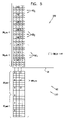
- FIG. 5 is a diagram showing a snapshot of cells scanned by an array of the apparatus of FIGS. 1A or 1 B, according to the alternative embodiment of the present invention
- FIG. 6 is a diagram showing parameters of scanned rectangles after a number of scans of the apparatus of FIGS. 1A or 1 B have been made, according to the alternative embodiment of the present invention
- FIG. 7 is a diagram showing a relation between a scanned field of view and dimensions of dies being scanned, according to an embodiment of the present invention.
- FIG. 8 is a diagram illustrating a method for maintaining die periodicity, according to an embodiment of the present invention.
- Embodiments of the present invention focus an array of beams to an array of respective spots on a surface, and relate to methods for scanning the spots over the surface.
- Substantially any type of beam i.e., beams of particles, or beams of waves, may be used.
- the beams may be charged particle beams, the charged particles being positive or negative ions or electrons.
- the beams may consist of electromagnetic waves from substantially any part of the electromagnetic spectrum, such as waves in the visible, near-visible, and/or X-ray regions of the spectrum.
- FIG. 1A is a schematic illustration of an optical inspection apparatus 10 , according to an embodiment of the present invention.
- Apparatus 10 has a light source 12 , typically a laser source, which is divided by a beam multiplexer 14 into an array 16 of generally parallel beams.
- a cross-section 18 of array 16 is symmetrical.
- cross-section 18 is assumed to have six-fold symmetry, i.e., nearest neighbors of elements of the cross-section are at the vertices of equilateral triangles.
- cross-section 18 may have any other convenient form of symmetry, such as two-, three-, or four-fold symmetry.
- any other convenient system such as a multiplicity of generally similar beam sources, may be used to generate array 16 , and that all such systems are assumed to be comprised within the scope of the present invention.
- a processor 36 operates the elements of apparatus 10 .
- Objective optics 20 direct and focus beam array 16 onto a plane surface 22 of an element 24 , producing an array of focused spots 27 on the plane surface of the element.
- Element 24 is mounted on a motion stage 38 .
- Surface 22 is assumed to contain orthogonal x and y axes, and to be normal to a z axis.
- Processor 36 is able to operate stage 38 so that surface 22 translates in an x and/or a y direction, or in any combination of these directions.
- Optics 20 comprise a scanner 28 , which is operated by processor 36 to scan focused spots 27 across surface 22 .
- Systems corresponding to optics 20 and scanner 28 are well known in the art, the latter typically comprising a mirror and/or acousto-optic elements for diverting beams 16 .
- optics 20 and scanner 28 may be implemented from substantially any elements which are able to focus beams 16 onto respective portions of surface 22 , and to scan the focused beams across the surface.
- Objective optics 20 may typically also be at least partly utilized as imaging optics 32 , the imaging optics forming images of respective spots 27 onto a detector array 34 . Signals from array 34 are processed by processor 36 .
- scanner 28 is typically able to scan beam array 16 so that spots array 27 moves across relatively large areas of surface 22
- Region 30 is typically an approximately oval region, approximately symmetrically located with respect to an optical axis 29 of apparatus 10 .
- Region 30 is herein assumed to be contained within an approximately square region of side 500 ⁇ m.
- scanner 28 maintains focused spot array 27 substantially within aberration-corrected region 30 .
- FIG. 1B is a schematic illustration of a charged particle inspection apparatus 50 , according to an embodiment of the present invention.
- Apparatus 50 may also be used to inspect element 24 , which as for apparatus 10 , is assumed to be mounted on stage 38 .
- Apparatus 50 comprises a charged particle source 52 , herein assumed by way of example to be an electron source, which generates an ordered array of charged particle beams 54 .
- Beams 54 pass through a scanner 58 and a beam splitter 56 , comprised in electron optics 57 , so as to create a focused spot array 60 on surface 22 .
- Spot array 60 is assumed to be generally similar to array 27 .
- a detector 62 collects secondary electrons (SE) or backscattered electrons (BE), which are directed to the detector by beam splitter 56 .
- An imager 64 receives signals from detector 62 , and in response generates an SE or a BE image of surface 22 .
- Elements of apparatus 50 are operated by a processor 68 .
- scanner 58 is typically able to scan focused spot array 60 so that the spots move across relatively large areas of surface 22
- Region 70 typically has properties generally similar to those described above for region 30 , and is herein assumed to be approximately symmetrically located with respect to an axis 72 of optics 57 .
- scanner 58 maintains focused spot array 60 substantially within aberration-corrected region 70 .
- Apparatus 10 and apparatus 50 may be used, inter alia, for inspection and/or for photolithography of wafers and/or reticles.
- element 24 comprises a semiconductor wafer having a plurality of substantially identical dies 25
- apparatus 10 or apparatus 50 is used to inspect surface 22 of the wafer.
- the following description is generally drawn to embodiments wherein the beams are generated using a particular type of electromagnetic wave, using optical inspection apparatus 10 . It will be appreciated that this is by way of example, and those skilled in the art will be able to adapt the description to spots produced by any type of wave beam. It will also be appreciated that those skilled in the art will be able to adapt the description, mutatis mutandis, to inspection by substantially any type of particle beam apparatus, such as charged particle inspection apparatus 50 .
- FIG. 1C is an enlargement of a section of FIG. 1A , showing region 30 , array 27 , and dies 25 in more detail, according to an embodiment of the present invention.
- processor 36 operates stage 38 and scanner 28 of apparatus 10 so that a swathe 39 is scanned across surface 22 , and typically so that other swathes 13 are also scanned across the surface.
- FIGS. 2A and 2B are schematic diagrams illustrating focused spots 27 in region 30 , according to an embodiment of the present invention.
- spots 27 are formed as 59 columns of 26 rows of spots, so that there are a total of 1534 spots, formed from a corresponding 1534 beams generated by multiplexer 14.
- the columns of spots define a beam array axis, and may be set to be parallel to the y axis.
- Each of the spots is assumed to be equidistant from its nearest neighbors, the distance being 10 ⁇ m.
- the above numerical values and orientation for spots 27 are provided by way of example, and that embodiments of the present invention may use substantially any convenient number, separation, and orientation of the spots.
- a different number of spots is used, in an array generally similar in form to that described herein with respect to FIGS. 2A and 2B , in an alternative embodiment described with reference to FIGS. 4-6 .
- Spots 27 are initially positioned to be in an upper portion 32 of region 30 .
- terms such as “upper,” “lower,” and “left-side,” when used in relation to spots 27 are used to clarify the description, and refer to positions within FIGS. 2A and 2B and other figures herein, not to an aspect of apparatus 10 .
- surface 22 FIGS. 1A and 1C
- V stage in the y direction
- the array moves with two components which are added vectorially: a component V stage , and a raster scan 80 component.
- An enlarged section I of raster scan 80 is shown in FIG. 2B , and in enlarged section I, individual spots of array 27 are labeled A 1 , A 2 , . . . , B 1 , B 2 , . . . , where A, B, . . . are column labels, and 1 , 2 , . . . are row labels.
- Enlarged section I illustrates the raster pattern of spots 27 due to raster scan 80 alone, and corresponds to the motion of the spots as seen by an imaginary observer on moving surface 22 .
- Processor 36 sets the raster scan so that each spot of array 27 scans a substantially similar 10 ⁇ m ⁇ 8.66 ⁇ m rectangle 82 , by scanning a predetermined number of rows within the rectangle that are perpendicular to the y-direction. As described further below, the actual number of rows scanned depends on a size of scanned pixels in rectangle 82
- Rectangles 82 generated by the raster scan, are contiguous and are arranged so that there are no gaps between rectangles.
- spot A 1 will be at a point 84 , and an approximately rectangular region 86 of surface 22 , shown in more detail in section II of FIG. 2B , will have been scanned by array 27 .
- V stage the position of array 27 will have moved from its initial upper portion 32 .
- V stage 0, the only movement of the array is because of the raster scan, and the position of array 27 remains substantially in upper portion 32 .
- Processor 36 sets the value of V stage so that at the conclusion of the raster scan, bottom line 88 of region 86 is approximately coincident with a bottom line 31 of region 30 ( FIG. 2A ). In other words, during one scan, processor 36 moves array 27 from upper portion 32 to a lower portion 33 of region 30 . As described in more detail below with reference to FIG.
- processor 36 repositions array 27 back to its initial position in upper portion 32 , and the processor then repeats the raster scan, while continuing to move the array and surface 22 with velocities V stage .
- the speed of the repositioning described herein, compared to the velocity V stage , is typically extremely high, so that the repositioning is essentially instantaneous.
- the time taken to reposition the array is less than 1% of the time for the array to scan.
- the time for the array to scan, T is described in relation to FIG. 3 and also in relation to expression (3) below.
- jump is also used to describe the repositioning that is implemented.
- FIG. 3 shows a schematic “snapshot” 100 after a number of the scans of swathe 39 have been performed, as described above, according to an embodiment of the present invention.
- four scans of substantially identical regions 86 of swathe 39 are assumed to have completed, and are shown in FIG. 3 as scans A, B, C, and D.
- Scan A is the first scan
- scan D is assumed to have just completed, so that apparatus 10 is about to begin a scan E.
- the position of region 30 is also shown in snapshot 100 .
- processor 36 After each scan A, B, . . . , processor 36 repositions the array in the negative y direction, by an amount that typically makes adjacent rectangles 86 contiguous with each other. In some embodiments of the present invention, processor 36 repositions the array so that there is a small overlap between adjacent rectangles 86 .
- a graph 107 of the y-position of array 27 vs. time is a saw-tooth graph, with the vertical lines 109 of the graph corresponding to the jumps applied to the array.
- T corresponds to the time for processor 36 to perform one scan of array 27 , time T being equal to the time taken to scan one rectangle 82 ( FIGS. 2A and 2B ).
- the value of T depends on the time taken by processor 36 to scan an individual pixel on surface 22 , and on the number of pixels scanned by each spot of array 27 . The latter also affects the number of rows scanned within each rectangle 82 .
- N pix the number of pixels N pix , and the number of rows R, scanned within a specific rectangle 82 .
- Processor 36 uses the value of T from expression (3) to adjust the value of V stage so that scans such as scan A and scan B ( FIG. 3 ) are contiguous or slightly overlapping. After each time T, processor 36 repositions array 27 to irradiate a new region of surface 22 . Using the values for array 27 given above, in the case of no overlap, processor 36 repositions array 27 260 ⁇ m in the negative y-direction after each scan has completed. The value of 260 ⁇ m corresponds to the y height of the 26 rows scanned by array 27 .
- processor 36 For an overlap between scans of 10 ⁇ m, corresponding to the height of one rectangle 82 , processor 36 repositions the array by 250 ⁇ m in the negative y-direction after each scan has completed. In either case, the value of V stage is given by expression (4):
- V stage FOV y T ( 4 )
- V stage given by expression (4) (and also that given by expression (8) below) may be reduced correspondingly, as will be apparent to those skilled in the art.
- swathe 39 is formed of contiguous or slightly overlapping regions 86 , each one of which scans a portion of surface 22 with substantially no un-scanned parts within the regions.
- apparatus 10 typically scans multiple swathes, each swathe either being contiguous with each other, or slightly overlapping.
- one or more second swathes 13 adjacent to swathe 39 , may be 511 ⁇ m from swathe 39 , measured along the x-axis, giving no overlap, or may be 502 ⁇ m along the x-axis from swathe 39 , giving an overlap of one rectangle 82 .
- embodiments of the present invention described with reference to FIGS. 2A , 2 B, and 3 provide a set of regions 86 , each of the regions having substantially no un-scanned parts. After each region 86 is scanned, array 27 is repositioned. Swathe 39 is then formed by “joining” adjacent regions 86 together.
- the same general pattern of scanning, repositioning the array in the negative y-direction, then scanning is followed. Also, as in the embodiments described above, surface 22 and array 27 are both moved with a y-velocity V stage , the array also having a scan imposed on its V stage motion.
- each specific scan of the alternative embodiment does have un-scanned regions. As is described below, the scans with un-scanned regions are combined together, and the combination eliminates the un-scanned regions.
- FIG. 4 is a schematic diagram illustrating focused spots 27 in region 30 , according to an alternative embodiment of the present invention.
- spots 27 are formed as 59 columns of 48 rows of spots, so that there are a total of 2832 spots, formed from a corresponding 2832 beams generated by multiplexer 14 .
- the columns of spots are set to be parallel to the y axis.
- Each of the spots is assumed to be equidistant to its nearest neighbors, the distance being 10 ⁇ m, so that each spot defines contiguous rectangles 82 having dimensions 10 ⁇ m ⁇ 8.66 ⁇ m, as described above with reference to FIGS. 2A and 2B .
- FIG. 4 unlike the embodiment described with reference to FIGS.
- FOV y and FOV x are respectively 480 ⁇ m and 511 ⁇ m.
- some embodiments of the present invention may use smaller reposition values, or jumps, than the size of the jumps described above with reference to FIGS. 2A , 2 B, and 3 . These smaller jumps are referred to herein as “sub-jumps,” and the time difference between sub-jumps is reduced from the time T described above.
- Each rectangle 82 is divided into a number of generally similar cells 110 .
- a respective cell 110 of every rectangle 82 is scanned using substantially the same method as described above for the embodiment of FIG. 2 , i.e., surface 22 is moved with velocity V stage , and array 27 is moved with a combination of the same velocity V stage and a raster scan that scans the specific cell.
- array 27 makes a sub-jump in the negative y-direction and another respective cell 110 of every rectangle 82 is scanned.
- the process of cell scanning and making sub-jumps in the negative y-direction continues. During an initial phase of the process, only some of the cells of rectangles 82 are scanned. Once the initial phase has completed, all the cells of the rectangles are scanned, so that continuing the process after the initial phase ensures that further rectangles 82 are completely scanned.
- the process for using the sub-jumps is described in more detail hereinbelow.
- each rectangle 82 there are assumed to be an integral number J of cells 110 .
- the value of J is related to the number M of rows of array 27 according to expression (5):
- I is a positive integer less than M.
- the number of pixels N pixc in each cell 110 , and the time T c needed to scan each cell, are given by expressions (6) and (7), respectively derived from expressions (2) and (3) above.
- N pixc 86.6 J ⁇ p 2 ( 6 )
- V stage FOV y J ⁇ T c ( 8 )
- array 27 After each time T c , i.e., after a cell 110 has been scanned, array 27 makes a sub-jump in the negative y-direction given by expression (9):
- cells 110 of rectangle 82 are assumed to be formed as a 4 ⁇ 4 array, but it will be appreciated that any other convenient array of 16 cells, such as a 2 ⁇ 8 array, may be used.
- the value of FOV y is 480 ⁇ m, so that from expression (9) the value of the sub-jump is 30 ⁇ m.
- a first set of cells e.g. cells 110 1
- T c time for the scan
- array 27 makes the sub-jump
- a different set of cells e.g., cells 110 3
- the process of scanning then sub-jumping continues.
- some of cells 110 of rectangles 82 are not scanned; once the initial scanning phase has completed, all cells 110 of every rectangle 82 are scanned.
- FIG. 5 is a diagram showing a snapshot 120 of cells 110 scanned by array 27 , according to the alternative embodiment of the present invention.
- Snapshot 120 is of the left-hand set of rectangles 82 of array 27 in FIG. 4 , and is shown after 15 sub-jumps have been made, so that 16 scans of array 27 have been made, a 16 th sub-jump is about to be made, and a 17 th scan is about to start.
- Snapshot 120 also shows a lower left margin of region 30 .
- cells that have been scanned during a first scan are labeled with “1”
- cells scanned during a second scan are labeled with “2”, . . .
- cells scanned during a 16 th scan are labeled with “16.”
- Other scanned cells are labeled with “/,” and cells that have not been scanned are empty.
- Snapshot 120 illustrates that after a first scan of cells 110 1 , a sub-jump of 30 ⁇ m in the negative y-direction is made, and a second scan of cells 110 3 is made.
- cells 110 2 are scanned, and once this scan has completed, all cells of the three sets of rectangles 82 closest to the lower edge of region 30 , labeled 82 1 , have been scanned.
- the process begins to repeat, i.e., un-scanned cells 110 1 are scanned, and during this scan, the V stage component applied to array 27 moves the three sets of rectangles 82 2 to the lower edge of region 30 .
- the V stage component applied to array 27 moves the three sets of rectangles 82 2 to the lower edge of region 30 .
- the 18 th scan rectangles 82 3 will be closest to the lower edge of region 30 , and will have been completely scanned.
- FIG. 6 is a diagram 130 showing parameters of scanned rectangles 82 after 21 scans have been made, according to the alternative embodiment of the present invention. After each scan a sub-jump equal to the y-height of three rectangles 82 is made.
- a column 132 refers to the set of rectangles 82 1 , . . . by the subscript of the rectangles, and it will be understood that each set comprises three rectangles 82 .
- a region 134 of the diagram shows cells scanned during each scan; in the region the cells are referred to by their subscripts.
- the relative beam positions of the spots generated by array 27 do not need to be very accurate, and that any inaccuracies may be taken care of by including a small overlap between cells 110 .
- the value of FOV y for array 27 may be set to be nearly equal to the y-value of aberration-corrected region 30 .
- FIG. 7 is a diagram 150 showing a relation between the scanned FOV y and the dimensions of dies 25 , according to an embodiment of the present invention.
- dies 25 of surface 22 are rectangular with substantially identical external dimensions.
- die periodicity This condition is herein termed “die periodicity.” It will be understood that maintaining die periodicity facilitates die-to-die comparisons; other applications where maintaining die periodicity is advantageous will be apparent to those skilled in the art.
- each die 25 is D y . If the y-dimension of each die 25 is D y , then identical locations of dies will be scanned by the same spot of array 27 , i.e., die periodicity holds, when an integral number of scans exactly fill the die, corresponding to expression (10) being true:
- I is a positive integer
- each die 25 has an unscanned region 156 , and die periodicity does not hold.
- a relatively small change of magnification of array 27 may be made, changing the value of FOV y so that expression (10) is true. For example, if FOV y is changed to 481.25 ⁇ m, then
- FIG. 8 is a diagram 170 illustrating an alternative method for maintaining die periodicity, according to an embodiment of the present invention.
- processor 36 applies two different sized sub-jumps to array 27 , as shown in a row 174 , wherein “A” indicates a sub-jump of one size and “B” indicates a sub-jump of a different size.
- Processor 36 also adjusts the velocity V stage of stage 38 so that the constant distance Y stage traveled by stage 38 during each of the sub-jumps lies between the two sub-jump sizes.
- processor 36 adjusts their number so that they exactly total a die size D y , shown in row 172 .
- Processor 36 also adjusts the numbers of the two sub-jumps, A, B, so that the total distance traversed by the sub-jumps is exactly equal to D y .
- Nby the number of rows of spots in array 27 ;
- Ncell the number of cells per rectangle 82 ;
- N by J ⁇ N cell (11)
- D y D ⁇ pitch+ d (0 ⁇ d ⁇ pitch)
- D E ⁇ Nby ⁇ F (0 ⁇ F ⁇ NBy ) (12)
- Processor 36 implements N J sub-jumps of size Y J and N J-1 sub-jumps of size Y J-1 , where:
- N J ( E ⁇ Ncell - F )
- ⁇ Y J - 1 ( J - 1 ) ⁇ D y D ( 13 )
- processor 36 After each sub-jump, processor 36 sets array 27 to scan a different cell, from 1 to Ncell, of rectangles 82 , and repeats the scanning sequence.
- the total number of sub-jumps, N J +N J-1 is E ⁇ Ncell. Since E is an integer, this is an integral multiple of Ncell, so that each period begins on the same cell as the previous period.
- Processor 36 sets the velocity of stage 38 , V stage , so that between sub-jumps, i.e., during the scanning of each cell, the stage moves in the y-direction by the value given by expression (14) below. Since processor 36 moves array 27 with the same velocity V stage during scanning of the array, array 27 moves in the y-direction by the same amount.
- Expression (15) can be simplified, using expressions (11), (12) and (13) as follows:
- Expression (16) shows that the total distance traversed by all the sub-jumps is D y ; since, as described above, each period begins on the same cell as the previous period, die periodicity is maintained.
- the two sub-jumps calculated above may be interspersed in any convenient manner.
- the interspersion is performed so that array 27 deviates as little as possible from axis 29 of apparatus 10 .
- Methods for calculating such interspersion are well known in the art; following are two Matlab functions that may be used to calculate a satisfactory interspersion:
- embodiments of the present invention significantly relax tolerances on beam positions for both optical and particle beams, since there is no relationship between the direction of motion of the scanning stage and the positions of the beams within their array. Furthermore, embodiments of the present invention significantly increase the size of the array that may be used, while enabling the array to be kept within a specific region, such as an aberration-free region. Also, embodiments of the present invention enable die periodicity to be maintained, without compromising on the advantages described above.
Abstract
Description
FOV y ×FOV x=260 μm×511μm (1)
-
- where FOVy is the y Field of View value of the scanned region, and
- FOVx is the x Field of View value of the scanned region.
- where FOVy is the y Field of View value of the scanned region, and
and die periodicity holds, as is illustrated by
Nby=J·Ncell (11)
D y =D·pitch+d(0≦d≦pitch)
D=E·Nby−F(0 ≦F<NBy) (12)
NJ·YJ+NJ−1·YJ−1 (15)
-
- Example I: NJ=484, YJ=30 μm;
- NJ-1=44, YJ-1=20 μm.
- Example II: NJ=483, YJ=30.019 μm;
- NJ-1=45, YJ-1=20.013 μm.
| function [NJ, NJ1, Ystage, YJ, YJ1, overhead] = APBS_algo(Dy, |
| pitch, J, Ncell); |
| D = fix(Dy / pitch); d = Dy − D*pitch; |
| NBy = J*Ncell; E = 1 + fix((D−1)/NBy); F = E*NBy − D; |
| NJ = E*Ncell−F; YJ = J* Dy./D; |
| NJ1 = F; YJ1 = (J−1)*Dy./D; |
| N = NJ + NJ1; % total number of jumps |
| Ystage = die ./ N; |
| overhead = (J−1)*d./die + pitch*F./die; |
| return |
| function [Jump] = APBS_jump(Dy, pitch, J, Ncell); |
| % Jump = output vector of optimal jump sequence |
| % (example: [J J J−1 J ... ]′ ) |
| [NJ, NJ1, Ystage, YJ, YJ1, overhead] = APBS_algo(Dy, pitch, J, Ncell); |
| N = NJ + NJ1; dY = YJ − Ystage; dY1 = YJ1 − Ystage; |
| Jump = [J]; Offset = dY; |
| for i=2:N, |
| Offset_J = Offset + dY; Offset_J1 = Offset + dY1; |
| if abs(Offset_J)< abs(Offset_J1), Jump = [Jump; J]; Offset = |
| Offset_J; |
| else Jump = [Jump; J−1]; Offset = Offset_J1; |
| end |
| end |
| return |
Claims (20)
Priority Applications (2)
| Application Number | Priority Date | Filing Date | Title |
|---|---|---|---|
| US11/334,963 US7468506B2 (en) | 2005-01-26 | 2006-01-19 | Spot grid array scanning system |
| US11/339,044 US7468507B2 (en) | 2005-01-26 | 2006-01-25 | Optical spot grid array scanning system |
Applications Claiming Priority (2)
| Application Number | Priority Date | Filing Date | Title |
|---|---|---|---|
| US64797005P | 2005-01-26 | 2005-01-26 | |
| US11/334,963 US7468506B2 (en) | 2005-01-26 | 2006-01-19 | Spot grid array scanning system |
Related Child Applications (1)
| Application Number | Title | Priority Date | Filing Date |
|---|---|---|---|
| US11/339,044 Continuation-In-Part US7468507B2 (en) | 2005-01-26 | 2006-01-25 | Optical spot grid array scanning system |
Publications (2)
| Publication Number | Publication Date |
|---|---|
| US20060261261A1 US20060261261A1 (en) | 2006-11-23 |
| US7468506B2 true US7468506B2 (en) | 2008-12-23 |
Family
ID=37447489
Family Applications (1)
| Application Number | Title | Priority Date | Filing Date |
|---|---|---|---|
| US11/334,963 Expired - Fee Related US7468506B2 (en) | 2005-01-26 | 2006-01-19 | Spot grid array scanning system |
Country Status (1)
| Country | Link |
|---|---|
| US (1) | US7468506B2 (en) |
Cited By (29)
| Publication number | Priority date | Publication date | Assignee | Title |
|---|---|---|---|---|
| US20090242761A1 (en) * | 2008-03-31 | 2009-10-01 | Hermes-Microvision, Inc. | Method and apparatus for charged particle beam inspection |
| US8791656B1 (en) | 2013-05-31 | 2014-07-29 | Mevion Medical Systems, Inc. | Active return system |
| US8907311B2 (en) | 2005-11-18 | 2014-12-09 | Mevion Medical Systems, Inc. | Charged particle radiation therapy |
| US8927950B2 (en) | 2012-09-28 | 2015-01-06 | Mevion Medical Systems, Inc. | Focusing a particle beam |
| US8933650B2 (en) | 2007-11-30 | 2015-01-13 | Mevion Medical Systems, Inc. | Matching a resonant frequency of a resonant cavity to a frequency of an input voltage |
| US8941083B2 (en) | 2007-10-11 | 2015-01-27 | Mevion Medical Systems, Inc. | Applying a particle beam to a patient |
| US8952634B2 (en) | 2004-07-21 | 2015-02-10 | Mevion Medical Systems, Inc. | Programmable radio frequency waveform generator for a synchrocyclotron |
| US8970137B2 (en) | 2007-11-30 | 2015-03-03 | Mevion Medical Systems, Inc. | Interrupted particle source |
| US9155186B2 (en) | 2012-09-28 | 2015-10-06 | Mevion Medical Systems, Inc. | Focusing a particle beam using magnetic field flutter |
| US9185789B2 (en) | 2012-09-28 | 2015-11-10 | Mevion Medical Systems, Inc. | Magnetic shims to alter magnetic fields |
| US9301384B2 (en) | 2012-09-28 | 2016-03-29 | Mevion Medical Systems, Inc. | Adjusting energy of a particle beam |
| US9545528B2 (en) | 2012-09-28 | 2017-01-17 | Mevion Medical Systems, Inc. | Controlling particle therapy |
| US9622335B2 (en) | 2012-09-28 | 2017-04-11 | Mevion Medical Systems, Inc. | Magnetic field regenerator |
| US9661736B2 (en) | 2014-02-20 | 2017-05-23 | Mevion Medical Systems, Inc. | Scanning system for a particle therapy system |
| US9681531B2 (en) | 2012-09-28 | 2017-06-13 | Mevion Medical Systems, Inc. | Control system for a particle accelerator |
| US9723705B2 (en) | 2012-09-28 | 2017-08-01 | Mevion Medical Systems, Inc. | Controlling intensity of a particle beam |
| US9730308B2 (en) | 2013-06-12 | 2017-08-08 | Mevion Medical Systems, Inc. | Particle accelerator that produces charged particles having variable energies |
| US9950194B2 (en) | 2014-09-09 | 2018-04-24 | Mevion Medical Systems, Inc. | Patient positioning system |
| US9962560B2 (en) | 2013-12-20 | 2018-05-08 | Mevion Medical Systems, Inc. | Collimator and energy degrader |
| US10254739B2 (en) | 2012-09-28 | 2019-04-09 | Mevion Medical Systems, Inc. | Coil positioning system |
| US10258810B2 (en) | 2013-09-27 | 2019-04-16 | Mevion Medical Systems, Inc. | Particle beam scanning |
| US20200051777A1 (en) * | 2018-08-07 | 2020-02-13 | Applied Materials Israel Ltd. | Method for evaluating a region of an object |
| US10646728B2 (en) | 2015-11-10 | 2020-05-12 | Mevion Medical Systems, Inc. | Adaptive aperture |
| US10653892B2 (en) | 2017-06-30 | 2020-05-19 | Mevion Medical Systems, Inc. | Configurable collimator controlled using linear motors |
| US10675487B2 (en) | 2013-12-20 | 2020-06-09 | Mevion Medical Systems, Inc. | Energy degrader enabling high-speed energy switching |
| US10925147B2 (en) | 2016-07-08 | 2021-02-16 | Mevion Medical Systems, Inc. | Treatment planning |
| US11103730B2 (en) | 2017-02-23 | 2021-08-31 | Mevion Medical Systems, Inc. | Automated treatment in particle therapy |
| US11291861B2 (en) | 2019-03-08 | 2022-04-05 | Mevion Medical Systems, Inc. | Delivery of radiation by column and generating a treatment plan therefor |
| US11469076B2 (en) | 2018-06-12 | 2022-10-11 | Asml Netherlands B.V. | System and method for scanning a sample using multi-beam inspection apparatus |
Families Citing this family (4)
| Publication number | Priority date | Publication date | Assignee | Title |
|---|---|---|---|---|
| US7468507B2 (en) * | 2005-01-26 | 2008-12-23 | Applied Materials, Israel, Ltd. | Optical spot grid array scanning system |
| US7468506B2 (en) | 2005-01-26 | 2008-12-23 | Applied Materials, Israel, Ltd. | Spot grid array scanning system |
| JP5709465B2 (en) * | 2010-10-29 | 2015-04-30 | キヤノン株式会社 | Drawing apparatus and article manufacturing method |
| EP2705354B1 (en) | 2011-05-03 | 2016-01-20 | Applied Materials Israel, Ltd. | Multi-spot collection optics |
Citations (34)
| Publication number | Priority date | Publication date | Assignee | Title |
|---|---|---|---|---|
| US5892224A (en) | 1996-05-13 | 1999-04-06 | Nikon Corporation | Apparatus and methods for inspecting wafers and masks using multiple charged-particle beams |
| US5973332A (en) * | 1996-03-04 | 1999-10-26 | Canon Kabushiki Kaisha | Electron beam exposure method, and device manufacturing method using same |
| US6028306A (en) * | 1997-05-14 | 2000-02-22 | Olympus Optical Co., Ltd. | Scanning microscope |
| US20010052576A1 (en) | 2000-03-31 | 2001-12-20 | Yasuhiro Shimada | Electron optical system array, method of manufacturing the same, charged-particle beam exposture apparatus, and device manufacturing method |
| US20010054690A1 (en) | 2000-03-31 | 2001-12-27 | Yasuhiro Shimada | Electron optical system array, method of fabricating the same, charged-particle beam exposure apparatus, and device manufacturing method |
| US20020028399A1 (en) | 2000-06-27 | 2002-03-07 | Mamoru Nakasuji | Inspection system by charged particle beam and method of manufacturing devices using the system |
| US20020033449A1 (en) | 2000-06-27 | 2002-03-21 | Mamoru Nakasuji | Inspection system by charged particle beam and method of manufacturing devices using the system |
| US20020109090A1 (en) | 2000-12-12 | 2002-08-15 | Mamoru Nakasuji | Electron beam apparatus and method of manufacturing semiconductor device using the apparatus |
| US20020130262A1 (en) | 2000-11-17 | 2002-09-19 | Mamoru Nakasuji | Method for inspecting substrate, substrate inspecting system and electron beam apparatus |
| US20020142486A1 (en) | 2001-03-28 | 2002-10-03 | Shusaku Yanagawa | Method of fabricating semiconductor device |
| US6465783B1 (en) * | 1999-06-24 | 2002-10-15 | Nikon Corporation | High-throughput specimen-inspection apparatus and methods utilizing multiple parallel charged particle beams and an array of multiple secondary-electron-detectors |
| US20020148961A1 (en) | 2000-11-02 | 2002-10-17 | Mamoru Nakasuji | Electron beam apparatus and device production method using the electron beam apparatus |
| US6504147B1 (en) * | 1999-11-15 | 2003-01-07 | Brother Kogyo Kabushiki Kaisha | Multibeam scanner |
| US6593152B2 (en) | 2000-11-02 | 2003-07-15 | Ebara Corporation | Electron beam apparatus and method of manufacturing semiconductor device using the apparatus |
| US20030156280A1 (en) | 2002-02-21 | 2003-08-21 | Applied Materials, Inc. | Multi beam scanning with bright/dark field imaging |
| US20030179369A1 (en) | 2002-03-22 | 2003-09-25 | Applied Materials, Inc | Wafer defect detection system with traveling lens multi-beam scanner |
| US20030184835A1 (en) | 2002-01-14 | 2003-10-02 | Boris Goldberg | Multi-beam polygon scanning system |
| US20030227618A1 (en) | 2002-05-06 | 2003-12-11 | Applied Materials Israel Ltd | High speed laser scanning inspection system |
| US6740896B2 (en) * | 2002-04-24 | 2004-05-25 | Renesas Technology Corp. | Sensitivity adjusting method for pattern inspection apparatus |
| US20040119023A1 (en) * | 2001-06-15 | 2004-06-24 | Ebara Corporation | Electron beam apparatus and a device manufacturing method by using said electron beam apparatus |
| US20050024881A1 (en) | 2003-07-30 | 2005-02-03 | Jack Lin | Shade structure of lamps |
| WO2005024881A2 (en) | 2003-09-05 | 2005-03-17 | Carl Zeiss Smt Ag | Particle-optical systems, components and arrangements |
| US20050074002A1 (en) | 2003-10-01 | 2005-04-07 | Nortel Networks Limited | Selective forwarding of damaged packets |
| US6936810B2 (en) | 2003-07-21 | 2005-08-30 | Thomas Hiramatsu-Tie | Method and apparatus for scanning an optical beam using an optical conduit |
| WO2005103657A1 (en) | 2004-04-15 | 2005-11-03 | Applied Materials Israel, Ltd. | A high throughput multi beam detection system and method |
| US20060012791A1 (en) | 2004-06-22 | 2006-01-19 | Silviu Reinhorn | Wafer inspection system |
| US20060060789A1 (en) | 2004-01-29 | 2006-03-23 | Rogers Steven R | Focusing system and method for a charged particle imaging system |
| US7067830B2 (en) * | 2002-07-30 | 2006-06-27 | Hitachi, Ltd. | Multi-electron beam exposure method and apparatus |
| US20060261261A1 (en) | 2005-01-26 | 2006-11-23 | Rogers Steven R | Spot grid array scanning system |
| US20070028596A1 (en) | 1993-04-09 | 2007-02-08 | Hitachi, Ltd. | Diagnostic equipment for an exhaust gas cleaning apparatus |
| US20070028595A1 (en) | 2005-07-25 | 2007-02-08 | Mongia Hukam C | High pressure gas turbine engine having reduced emissions |
| US20070060017A1 (en) | 2005-09-13 | 2007-03-15 | Klusmeyer Toby L | Combination drinking container and electronic audio amplification device |
| US7223973B2 (en) | 2000-12-01 | 2007-05-29 | Ebara Corporation | Apparatus for inspection with electron beam, method for operating same, and method for manufacturing semiconductor device using former |
| US20070133077A1 (en) | 2005-01-26 | 2007-06-14 | Rogers Steven R | Optical spot grid array scanning system |
-
2006
- 2006-01-19 US US11/334,963 patent/US7468506B2/en not_active Expired - Fee Related
Patent Citations (43)
| Publication number | Priority date | Publication date | Assignee | Title |
|---|---|---|---|---|
| US20070028596A1 (en) | 1993-04-09 | 2007-02-08 | Hitachi, Ltd. | Diagnostic equipment for an exhaust gas cleaning apparatus |
| US5973332A (en) * | 1996-03-04 | 1999-10-26 | Canon Kabushiki Kaisha | Electron beam exposure method, and device manufacturing method using same |
| US5892224A (en) | 1996-05-13 | 1999-04-06 | Nikon Corporation | Apparatus and methods for inspecting wafers and masks using multiple charged-particle beams |
| US6028306A (en) * | 1997-05-14 | 2000-02-22 | Olympus Optical Co., Ltd. | Scanning microscope |
| US6465783B1 (en) * | 1999-06-24 | 2002-10-15 | Nikon Corporation | High-throughput specimen-inspection apparatus and methods utilizing multiple parallel charged particle beams and an array of multiple secondary-electron-detectors |
| US6504147B1 (en) * | 1999-11-15 | 2003-01-07 | Brother Kogyo Kabushiki Kaisha | Multibeam scanner |
| US20010052576A1 (en) | 2000-03-31 | 2001-12-20 | Yasuhiro Shimada | Electron optical system array, method of manufacturing the same, charged-particle beam exposture apparatus, and device manufacturing method |
| US20010054690A1 (en) | 2000-03-31 | 2001-12-27 | Yasuhiro Shimada | Electron optical system array, method of fabricating the same, charged-particle beam exposure apparatus, and device manufacturing method |
| US20020033449A1 (en) | 2000-06-27 | 2002-03-21 | Mamoru Nakasuji | Inspection system by charged particle beam and method of manufacturing devices using the system |
| US20020028399A1 (en) | 2000-06-27 | 2002-03-07 | Mamoru Nakasuji | Inspection system by charged particle beam and method of manufacturing devices using the system |
| US7135676B2 (en) | 2000-06-27 | 2006-11-14 | Ebara Corporation | Inspection system by charged particle beam and method of manufacturing devices using the system |
| US7247848B2 (en) | 2000-11-02 | 2007-07-24 | Ebara Corporation | Electron beam apparatus and method of manufacturing semiconductor device using the apparatus |
| US7244932B2 (en) | 2000-11-02 | 2007-07-17 | Ebara Corporation | Electron beam apparatus and device fabrication method using the electron beam apparatus |
| US20020148961A1 (en) | 2000-11-02 | 2002-10-17 | Mamoru Nakasuji | Electron beam apparatus and device production method using the electron beam apparatus |
| US6593152B2 (en) | 2000-11-02 | 2003-07-15 | Ebara Corporation | Electron beam apparatus and method of manufacturing semiconductor device using the apparatus |
| US7109483B2 (en) | 2000-11-17 | 2006-09-19 | Ebara Corporation | Method for inspecting substrate, substrate inspecting system and electron beam apparatus |
| US20020130262A1 (en) | 2000-11-17 | 2002-09-19 | Mamoru Nakasuji | Method for inspecting substrate, substrate inspecting system and electron beam apparatus |
| US7223973B2 (en) | 2000-12-01 | 2007-05-29 | Ebara Corporation | Apparatus for inspection with electron beam, method for operating same, and method for manufacturing semiconductor device using former |
| US20020109090A1 (en) | 2000-12-12 | 2002-08-15 | Mamoru Nakasuji | Electron beam apparatus and method of manufacturing semiconductor device using the apparatus |
| US7095022B2 (en) | 2000-12-12 | 2006-08-22 | Ebara Corporation | Electron beam apparatus and method of manufacturing semiconductor device using the apparatus |
| US7129485B2 (en) | 2000-12-12 | 2006-10-31 | Ebara Corporation | Electron beam apparatus and method of manufacturing semiconductor device using the apparatus |
| US20020142486A1 (en) | 2001-03-28 | 2002-10-03 | Shusaku Yanagawa | Method of fabricating semiconductor device |
| US20040119023A1 (en) * | 2001-06-15 | 2004-06-24 | Ebara Corporation | Electron beam apparatus and a device manufacturing method by using said electron beam apparatus |
| US20030184835A1 (en) | 2002-01-14 | 2003-10-02 | Boris Goldberg | Multi-beam polygon scanning system |
| US20030156280A1 (en) | 2002-02-21 | 2003-08-21 | Applied Materials, Inc. | Multi beam scanning with bright/dark field imaging |
| US20030179369A1 (en) | 2002-03-22 | 2003-09-25 | Applied Materials, Inc | Wafer defect detection system with traveling lens multi-beam scanner |
| US6740896B2 (en) * | 2002-04-24 | 2004-05-25 | Renesas Technology Corp. | Sensitivity adjusting method for pattern inspection apparatus |
| US20030227618A1 (en) | 2002-05-06 | 2003-12-11 | Applied Materials Israel Ltd | High speed laser scanning inspection system |
| US7067830B2 (en) * | 2002-07-30 | 2006-06-27 | Hitachi, Ltd. | Multi-electron beam exposure method and apparatus |
| US6936810B2 (en) | 2003-07-21 | 2005-08-30 | Thomas Hiramatsu-Tie | Method and apparatus for scanning an optical beam using an optical conduit |
| US20050024881A1 (en) | 2003-07-30 | 2005-02-03 | Jack Lin | Shade structure of lamps |
| US20060289804A1 (en) | 2003-09-05 | 2006-12-28 | Carl Zeiss Smt Ag | Particle-optical systems and arrangements and particle-optical components for such systems and arrangements |
| US7244949B2 (en) | 2003-09-05 | 2007-07-17 | Carl Zeiss Smt Ag | Particle-optical systems and arrangements and particle-optical components for such systems and arrangements |
| WO2005024881A2 (en) | 2003-09-05 | 2005-03-17 | Carl Zeiss Smt Ag | Particle-optical systems, components and arrangements |
| US20050074002A1 (en) | 2003-10-01 | 2005-04-07 | Nortel Networks Limited | Selective forwarding of damaged packets |
| US20060060789A1 (en) | 2004-01-29 | 2006-03-23 | Rogers Steven R | Focusing system and method for a charged particle imaging system |
| US20060023205A1 (en) | 2004-04-15 | 2006-02-02 | Applied Materials Israel Ltd | High throughput multi beam detection system and method |
| WO2005103657A1 (en) | 2004-04-15 | 2005-11-03 | Applied Materials Israel, Ltd. | A high throughput multi beam detection system and method |
| US20060012791A1 (en) | 2004-06-22 | 2006-01-19 | Silviu Reinhorn | Wafer inspection system |
| US20060261261A1 (en) | 2005-01-26 | 2006-11-23 | Rogers Steven R | Spot grid array scanning system |
| US20070133077A1 (en) | 2005-01-26 | 2007-06-14 | Rogers Steven R | Optical spot grid array scanning system |
| US20070028595A1 (en) | 2005-07-25 | 2007-02-08 | Mongia Hukam C | High pressure gas turbine engine having reduced emissions |
| US20070060017A1 (en) | 2005-09-13 | 2007-03-15 | Klusmeyer Toby L | Combination drinking container and electronic audio amplification device |
Cited By (51)
| Publication number | Priority date | Publication date | Assignee | Title |
|---|---|---|---|---|
| USRE48047E1 (en) | 2004-07-21 | 2020-06-09 | Mevion Medical Systems, Inc. | Programmable radio frequency waveform generator for a synchrocyclotron |
| US8952634B2 (en) | 2004-07-21 | 2015-02-10 | Mevion Medical Systems, Inc. | Programmable radio frequency waveform generator for a synchrocyclotron |
| US10279199B2 (en) | 2005-11-18 | 2019-05-07 | Mevion Medical Systems, Inc. | Inner gantry |
| US10722735B2 (en) | 2005-11-18 | 2020-07-28 | Mevion Medical Systems, Inc. | Inner gantry |
| US9925395B2 (en) | 2005-11-18 | 2018-03-27 | Mevion Medical Systems, Inc. | Inner gantry |
| US8907311B2 (en) | 2005-11-18 | 2014-12-09 | Mevion Medical Systems, Inc. | Charged particle radiation therapy |
| US8916843B2 (en) | 2005-11-18 | 2014-12-23 | Mevion Medical Systems, Inc. | Inner gantry |
| US9452301B2 (en) | 2005-11-18 | 2016-09-27 | Mevion Medical Systems, Inc. | Inner gantry |
| US8941083B2 (en) | 2007-10-11 | 2015-01-27 | Mevion Medical Systems, Inc. | Applying a particle beam to a patient |
| US8933650B2 (en) | 2007-11-30 | 2015-01-13 | Mevion Medical Systems, Inc. | Matching a resonant frequency of a resonant cavity to a frequency of an input voltage |
| USRE48317E1 (en) | 2007-11-30 | 2020-11-17 | Mevion Medical Systems, Inc. | Interrupted particle source |
| US8970137B2 (en) | 2007-11-30 | 2015-03-03 | Mevion Medical Systems, Inc. | Interrupted particle source |
| US8063363B2 (en) * | 2008-03-31 | 2011-11-22 | Hermes-Microvision, Inc. | Method and apparatus for charged particle beam inspection |
| US20120043462A1 (en) * | 2008-03-31 | 2012-02-23 | Hermes-Microvision, Inc. | Method and apparatus for charged particle beam inspection |
| US20090242761A1 (en) * | 2008-03-31 | 2009-10-01 | Hermes-Microvision, Inc. | Method and apparatus for charged particle beam inspection |
| US8497475B2 (en) * | 2008-03-31 | 2013-07-30 | Hermes-Microvision, Inc. | Method and apparatus for charged particle beam inspection |
| US8927950B2 (en) | 2012-09-28 | 2015-01-06 | Mevion Medical Systems, Inc. | Focusing a particle beam |
| US10155124B2 (en) | 2012-09-28 | 2018-12-18 | Mevion Medical Systems, Inc. | Controlling particle therapy |
| US9545528B2 (en) | 2012-09-28 | 2017-01-17 | Mevion Medical Systems, Inc. | Controlling particle therapy |
| US9681531B2 (en) | 2012-09-28 | 2017-06-13 | Mevion Medical Systems, Inc. | Control system for a particle accelerator |
| US9706636B2 (en) | 2012-09-28 | 2017-07-11 | Mevion Medical Systems, Inc. | Adjusting energy of a particle beam |
| US9723705B2 (en) | 2012-09-28 | 2017-08-01 | Mevion Medical Systems, Inc. | Controlling intensity of a particle beam |
| US9155186B2 (en) | 2012-09-28 | 2015-10-06 | Mevion Medical Systems, Inc. | Focusing a particle beam using magnetic field flutter |
| US10368429B2 (en) | 2012-09-28 | 2019-07-30 | Mevion Medical Systems, Inc. | Magnetic field regenerator |
| US9185789B2 (en) | 2012-09-28 | 2015-11-10 | Mevion Medical Systems, Inc. | Magnetic shims to alter magnetic fields |
| US9301384B2 (en) | 2012-09-28 | 2016-03-29 | Mevion Medical Systems, Inc. | Adjusting energy of a particle beam |
| US9622335B2 (en) | 2012-09-28 | 2017-04-11 | Mevion Medical Systems, Inc. | Magnetic field regenerator |
| US10254739B2 (en) | 2012-09-28 | 2019-04-09 | Mevion Medical Systems, Inc. | Coil positioning system |
| US8791656B1 (en) | 2013-05-31 | 2014-07-29 | Mevion Medical Systems, Inc. | Active return system |
| US9730308B2 (en) | 2013-06-12 | 2017-08-08 | Mevion Medical Systems, Inc. | Particle accelerator that produces charged particles having variable energies |
| US10258810B2 (en) | 2013-09-27 | 2019-04-16 | Mevion Medical Systems, Inc. | Particle beam scanning |
| US10456591B2 (en) | 2013-09-27 | 2019-10-29 | Mevion Medical Systems, Inc. | Particle beam scanning |
| US9962560B2 (en) | 2013-12-20 | 2018-05-08 | Mevion Medical Systems, Inc. | Collimator and energy degrader |
| US10675487B2 (en) | 2013-12-20 | 2020-06-09 | Mevion Medical Systems, Inc. | Energy degrader enabling high-speed energy switching |
| US9661736B2 (en) | 2014-02-20 | 2017-05-23 | Mevion Medical Systems, Inc. | Scanning system for a particle therapy system |
| US11717700B2 (en) | 2014-02-20 | 2023-08-08 | Mevion Medical Systems, Inc. | Scanning system |
| US10434331B2 (en) | 2014-02-20 | 2019-10-08 | Mevion Medical Systems, Inc. | Scanning system |
| US9950194B2 (en) | 2014-09-09 | 2018-04-24 | Mevion Medical Systems, Inc. | Patient positioning system |
| US10786689B2 (en) | 2015-11-10 | 2020-09-29 | Mevion Medical Systems, Inc. | Adaptive aperture |
| US11213697B2 (en) | 2015-11-10 | 2022-01-04 | Mevion Medical Systems, Inc. | Adaptive aperture |
| US10646728B2 (en) | 2015-11-10 | 2020-05-12 | Mevion Medical Systems, Inc. | Adaptive aperture |
| US11786754B2 (en) | 2015-11-10 | 2023-10-17 | Mevion Medical Systems, Inc. | Adaptive aperture |
| US10925147B2 (en) | 2016-07-08 | 2021-02-16 | Mevion Medical Systems, Inc. | Treatment planning |
| US11103730B2 (en) | 2017-02-23 | 2021-08-31 | Mevion Medical Systems, Inc. | Automated treatment in particle therapy |
| US10653892B2 (en) | 2017-06-30 | 2020-05-19 | Mevion Medical Systems, Inc. | Configurable collimator controlled using linear motors |
| US11469076B2 (en) | 2018-06-12 | 2022-10-11 | Asml Netherlands B.V. | System and method for scanning a sample using multi-beam inspection apparatus |
| US10811219B2 (en) * | 2018-08-07 | 2020-10-20 | Applied Materials Israel Ltd. | Method for evaluating a region of an object |
| US20200051777A1 (en) * | 2018-08-07 | 2020-02-13 | Applied Materials Israel Ltd. | Method for evaluating a region of an object |
| US11291861B2 (en) | 2019-03-08 | 2022-04-05 | Mevion Medical Systems, Inc. | Delivery of radiation by column and generating a treatment plan therefor |
| US11311746B2 (en) | 2019-03-08 | 2022-04-26 | Mevion Medical Systems, Inc. | Collimator and energy degrader for a particle therapy system |
| US11717703B2 (en) | 2019-03-08 | 2023-08-08 | Mevion Medical Systems, Inc. | Delivery of radiation by column and generating a treatment plan therefor |
Also Published As
| Publication number | Publication date |
|---|---|
| US20060261261A1 (en) | 2006-11-23 |
Similar Documents
| Publication | Publication Date | Title |
|---|---|---|
| US7468506B2 (en) | Spot grid array scanning system | |
| US7468507B2 (en) | Optical spot grid array scanning system | |
| KR102008669B1 (en) | Electron beam inspection apparatus and electron beam inspection method | |
| US6184526B1 (en) | Apparatus and method for inspecting predetermined region on surface of specimen using electron beam | |
| JP3689516B2 (en) | Electron beam exposure system | |
| US8658987B2 (en) | Circuit-pattern inspection device | |
| KR20190134494A (en) | Multi electron-beam image acquiring apparatus and positioning method of multi electron-beam optical system | |
| JPH09330867A (en) | Electron beam exposure method and manufacture of device using it | |
| KR102532712B1 (en) | Electron optical system and multi-beam image acquiring apparatus | |
| TWI721423B (en) | Multi-charged particle beam inspection device and multi-charged particle beam inspection method | |
| TW202015090A (en) | Multi-electron beam image acquisition apparatus, and multi-electron beam image acquisition method | |
| JP6649130B2 (en) | Pattern inspection apparatus and pattern inspection method | |
| JP6128744B2 (en) | Drawing apparatus, drawing method, and article manufacturing method | |
| US20090244078A1 (en) | Method and apparatus for obtaining images by raster scanning charged particle beam over patterned substrate on a continuous mode stage | |
| JP7126355B2 (en) | Charged particle beam inspection method | |
| JP2019211296A (en) | Electron beam inspection device and electron beam inspection method | |
| KR102371265B1 (en) | Multiple electron beams irradiation apparatus | |
| US11342157B2 (en) | Charged particle beam inspection apparatus and charged particle beam inspection method | |
| KR20130142923A (en) | Drawing apparatus, data processing method, and method of manufacturing article | |
| KR20240035873A (en) | Multi-electron beam image acquisition device and multi-electron beam image acquisition method | |
| TWI782516B (en) | Multi-electron beam image acquisition device and multi-electron beam image acquisition method | |
| TW202226315A (en) | Multibeam image acquisition apparatus and multibeam image acquisition method | |
| JP4477436B2 (en) | Charged particle beam exposure system | |
| US20010002301A1 (en) | Projection-exposure methods and apparatus exhibiting increased throughput | |
| JP3832914B2 (en) | Electron beam exposure apparatus and device manufacturing method using the apparatus |
Legal Events
| Date | Code | Title | Description |
|---|---|---|---|
| AS | Assignment |
Owner name: APPLIED MATERIALS ISRAEL, LTD., ISRAEL Free format text: ASSIGNMENT OF ASSIGNORS INTEREST;ASSIGNORS:ROGERS, STEVEN R.;ELMALIACH, NISSIM;ELYASEF, EMANUEL;AND OTHERS;REEL/FRAME:018041/0419;SIGNING DATES FROM 20060713 TO 20060720 |
|
| STCF | Information on status: patent grant |
Free format text: PATENTED CASE |
|
| AS | Assignment |
Owner name: APPLIED MATERIALS ISRAEL, LTD., ISRAEL Free format text: ASSIGNMENT OF ASSIGNORS INTEREST;ASSIGNOR:APPLIED MATERIALS ISRAEL, LTD.;REEL/FRAME:022039/0159 Effective date: 20081214 Owner name: CARL ZEISS AG, GERMANY Free format text: ASSIGNMENT OF ASSIGNORS INTEREST;ASSIGNOR:APPLIED MATERIALS ISRAEL, LTD.;REEL/FRAME:022039/0159 Effective date: 20081214 Owner name: APPLIED MATERIALS ISRAEL, LTD.,ISRAEL Free format text: ASSIGNMENT OF ASSIGNORS INTEREST;ASSIGNOR:APPLIED MATERIALS ISRAEL, LTD.;REEL/FRAME:022039/0159 Effective date: 20081214 Owner name: CARL ZEISS AG,GERMANY Free format text: ASSIGNMENT OF ASSIGNORS INTEREST;ASSIGNOR:APPLIED MATERIALS ISRAEL, LTD.;REEL/FRAME:022039/0159 Effective date: 20081214 |
|
| AS | Assignment |
Owner name: CARL ZEISS AG, GERMANY Free format text: ASSIGNMENT OF ASSIGNORS INTEREST;ASSIGNORS:LEO ELEKTRONENMIKROSKOPIE GMBH;CARL ZEISS SMS GMBH;CARL ZEISS NTS GMBH;AND OTHERS;SIGNING DATES FROM 20110901 TO 20110930;REEL/FRAME:027217/0248 Owner name: APPLIED MATERIALS ISRAEL, LTD., ISRAEL Free format text: ASSIGNMENT OF ASSIGNORS INTEREST;ASSIGNORS:LEO ELEKTRONENMIKROSKOPIE GMBH;CARL ZEISS SMS GMBH;CARL ZEISS NTS GMBH;AND OTHERS;SIGNING DATES FROM 20110901 TO 20110930;REEL/FRAME:027217/0248 |
|
| FPAY | Fee payment |
Year of fee payment: 4 |
|
| FPAY | Fee payment |
Year of fee payment: 8 |
|
| FEPP | Fee payment procedure |
Free format text: MAINTENANCE FEE REMINDER MAILED (ORIGINAL EVENT CODE: REM.); ENTITY STATUS OF PATENT OWNER: LARGE ENTITY |
|
| LAPS | Lapse for failure to pay maintenance fees |
Free format text: PATENT EXPIRED FOR FAILURE TO PAY MAINTENANCE FEES (ORIGINAL EVENT CODE: EXP.); ENTITY STATUS OF PATENT OWNER: LARGE ENTITY |
|
| STCH | Information on status: patent discontinuation |
Free format text: PATENT EXPIRED DUE TO NONPAYMENT OF MAINTENANCE FEES UNDER 37 CFR 1.362 |
|
| FP | Lapsed due to failure to pay maintenance fee |
Effective date: 20201223 |