US7468874B1 - Protection circuit for digital power module - Google Patents

Protection circuit for digital power module Download PDF

Info

Publication number
US7468874B1
US7468874B1 US11/269,192 US26919205A US7468874B1 US 7468874 B1 US7468874 B1 US 7468874B1 US 26919205 A US26919205 A US 26919205A US 7468874 B1 US7468874 B1 US 7468874B1
Authority
US
United States
Prior art keywords
state
mosfet
signal
voltage signal
detection
Prior art date
Legal status (The legal status is an assumption and is not a legal conclusion. Google has not performed a legal analysis and makes no representation as to the accuracy of the status listed.)
Expired - Fee Related, expires
Application number
US11/269,192
Inventor
Sam Yonghon Guo
Current Assignee (The listed assignees may be inaccurate. Google has not performed a legal analysis and makes no representation or warranty as to the accuracy of the list.)
Yazaki North America Inc
Original Assignee
Yazaki North America Inc
Priority date (The priority date is an assumption and is not a legal conclusion. Google has not performed a legal analysis and makes no representation as to the accuracy of the date listed.)
Filing date
Publication date
Application filed by Yazaki North America Inc filed Critical Yazaki North America Inc
Priority to US11/269,192 priority Critical patent/US7468874B1/en
Assigned to YAZAKI NORTH AMERICA, INC. reassignment YAZAKI NORTH AMERICA, INC. ASSIGNMENT OF ASSIGNORS INTEREST (SEE DOCUMENT FOR DETAILS). Assignors: GUO, SAM YONGHON
Assigned to YAZAKI NORTH AMERICA, INC. reassignment YAZAKI NORTH AMERICA, INC. CORRECTIVE ASSIGNMENT TO CORRECT THE EXECUTION DATE, PREVIOUSLY RECORDED AT REEL 017229, FRAME 0497. Assignors: GUO, SAM YONGHON
Application granted granted Critical
Publication of US7468874B1 publication Critical patent/US7468874B1/en
Expired - Fee Related legal-status Critical Current
Adjusted expiration legal-status Critical

Links

Images

Classifications

    • HELECTRICITY
    • H03ELECTRONIC CIRCUITRY
    • H03KPULSE TECHNIQUE
    • H03K17/00Electronic switching or gating, i.e. not by contact-making and –breaking
    • H03K17/08Modifications for protecting switching circuit against overcurrent or overvoltage
    • H03K17/082Modifications for protecting switching circuit against overcurrent or overvoltage by feedback from the output to the control circuit
    • H03K17/0822Modifications for protecting switching circuit against overcurrent or overvoltage by feedback from the output to the control circuit in field-effect transistor switches
    • HELECTRICITY
    • H03ELECTRONIC CIRCUITRY
    • H03KPULSE TECHNIQUE
    • H03K17/00Electronic switching or gating, i.e. not by contact-making and –breaking
    • H03K17/51Electronic switching or gating, i.e. not by contact-making and –breaking characterised by the components used
    • H03K17/56Electronic switching or gating, i.e. not by contact-making and –breaking characterised by the components used by the use, as active elements, of semiconductor devices
    • H03K17/687Electronic switching or gating, i.e. not by contact-making and –breaking characterised by the components used by the use, as active elements, of semiconductor devices the devices being field-effect transistors
    • H03K17/6877Electronic switching or gating, i.e. not by contact-making and –breaking characterised by the components used by the use, as active elements, of semiconductor devices the devices being field-effect transistors the control circuit comprising active elements different from those used in the output circuit

Definitions

  • the present invention relates to power MOSFETS, and more particularly to a protection circuit for a power MOSFET.
  • MOSFETs Metal-oxide semiconductor field effect transistors
  • ICs integrated circuits
  • a digital power module (DPM) for an automotive vehicle may include one or more power MOSFETs for solid-state power switching.
  • Vehicle body control functions and power distribution functions may be integrated on a vehicle DPM. These functions include, but are not limited to, interior and exterior lighting, windshield wipers, horn, air conditioning, clutch, fuel pump, starter relay, blower, system diagnostics, and/or smart fusing.
  • MOSFETS may provide the smart fusing and/or other functions in the DPM.
  • a circuit or device that includes a MOSFET may include current overload, short circuit, and/or over temperature protection elements.
  • a circuit may include a current sensor and/or a temperature sensor to detect when a MOSFET is exposed to one or more of the above conditions.
  • an exemplary MOSFET circuit 10 includes a smart or sense MOSFET 12 , a control circuit 14 , a gate resistor 16 , and a current detection resistor 18 .
  • the MOSFET 12 includes at least a gate terminal 20 , a source terminal 22 , a drain terminal 24 , and a current detection terminal 26 .
  • the gate terminal 20 is connected to an input voltage 28 through the gate resistor 16 .
  • the control circuit 14 senses a current through the current detection resistor 18 .
  • the current through the current detection resistor 18 is indicative of a current through the MOSFET 12 . Therefore, the control circuit 14 determines the current through the MOSFET 12 .
  • the control circuit 14 may determine when the current through the MOSFET 12 exceeds a particular threshold.
  • the MOSFET 12 may include TEM (temperature) MOSFET functions.
  • a TEM MOSFET includes one or more temperature detection terminals (not shown). The temperature detection terminals output a signal that is indicative of a temperature of the MOSFET 12 . In this manner, the control circuit 14 may determine when the temperature of the MOSFET 12 exceeds a particular threshold.
  • a MOSFET circuit relies on smart, sense, and/or TEM MOSFETs for current overload and/or over temperature protection.
  • Smart, sense, and TEM MOSFETs require additional terminals to provide the current/temperature sensing functions, thereby increasing package size and cost. Further, the additional terminals reduce space available for bonding wires.
  • a MOSFET circuit may include a power shunt resistor to sense a load current. However, in large current applications, the shunt resistor may generate significant heat, which is undesirable.
  • a sensorless protection circuit comprises a detection module.
  • the detection module receives a reference voltage signal and receives a load voltage signal from a MOSFET.
  • the detection module generates a detection signal having a first state and a second state according to the reference voltage signal and the load voltage signal.
  • a protection module receives the detection signal and maintains the MOSFET in an ON state when the detection signal is in the first state and transitions the MOSFET from the ON state to an OFF state when the detection signal is in the second state.
  • the detection signal is in the second state when the MOSFET is in at least one of a current overload condition, an over temperature condition, and a short circuit condition.
  • FIG. 1 is a circuit schematic of a MOSFET protection circuit that according to the prior art
  • FIG. 2 is a functional block diagram of a sensorless MOSFET protection circuit according to the present invention.
  • FIG. 3A is a functional block diagram of a sensorless MOSFET protection circuit according to the present invention.
  • FIG. 3B is a table that illustrates status indications of the MOSFET protection circuit according to the present invention.
  • FIG. 4 is a functional block diagram of a sensorless MOSFET protection circuit including a trial interval timer according to the present invention
  • FIG. 5 is a circuit schematic of a sensorless MOSFET protection circuit including a trial interval timer shown in more detail according to the present invention
  • FIG. 6 is a waveform illustration of a retrial interval for a short circuit test according to the present invention.
  • FIG. 7 is a waveform illustration of MOSFET energy consumption during a short circuit condition according to the present invention.
  • FIG. 8 is a functional block diagram of a sensorless MOSFET protection system according to the present invention.
  • module and/or device refers to an application specific integrated circuit (ASIC), an electronic circuit, a processor (shared, dedicated, or group) and memory that execute one or more software or firmware programs, a combinational logic circuit, and/or other suitable components that provide the described functionality.
  • ASIC application specific integrated circuit
  • processor shared, dedicated, or group
  • memory that execute one or more software or firmware programs, a combinational logic circuit, and/or other suitable components that provide the described functionality.
  • the protection circuit 50 includes a MOSFET 52 , a MOSFET driver module 54 , a detection module 56 , and a protection module 58 .
  • the MOSFET 52 includes a gate terminal 60 , a drain terminal 62 , and a source terminal 64 .
  • certain characteristics of a MOSFET are temperature sensitive. For example, a voltage drop across the drain terminal 62 and the source terminal 64 is indicative of a load current at a particular temperature of the MOSFET 52 . Similarly, a voltage drop across the drain terminal 62 and the source terminal 64 is indicative of a temperature of the MOSFET 52 at a particular load current. In other words, when certain characteristics of the MOSFET 52 are known, other characteristics, such as current and temperature, may be determined.
  • the source terminal 64 outputs a detection signal 66 .
  • the detection signal 66 is indicative of a temperature and/or a load current of the MOSFET 52 .
  • the detection module 56 receives the detection signal 66 and generates a detection output signal 68 .
  • the detection output signal 68 is indicative of whether the detection signal 66 is above or below a threshold.
  • the detection output signal 68 is indicative of a short circuit, current overload, and/or an over temperature condition.
  • the detection output signal 68 may be indicative of a startup inrush current condition.
  • the detection output signal 68 may be indicative of whether the detection signal 66 is within a range of values. When the detection signal 66 is within or outside the range of values, the detection output signal 68 is indicative of the short circuit, current overload, and/or over temperature condition.
  • the protection module 58 receives the detection output signal 68 and an input control signal 70 .
  • the detection output signal 68 indicates a short circuit, current overload, and/or over temperature condition
  • the protection module 58 turns OFF the MOSFET 52 .
  • the MOSFET 52 is ON, current flows from an power supply voltage (such as a battery voltage source) 72 , through the MOSFET 52 , to a load 74 .
  • the detection signal 66 is indicative of a voltage of the load 74 .
  • the MOSFET 52 is OFF, the MOSFET 52 prevents current flow to the load 74 .
  • the input control signal 70 is used to reset the protection module 58 and return the MOSFET 52 to an ON state.
  • the protection circuit 50 may include a high voltage reference module 80 and a low voltage reference module 82 .
  • the high voltage reference module 80 and the low voltage reference module 82 receive the power supply voltage 72 and generate a high voltage reference signal 84 and a low voltage reference signal 86 , respectively.
  • the high voltage reference module 80 and the low voltage reference module 82 generate voltage reference signals that are referenced to the power supply voltage 72 .
  • the high voltage reference signal 84 may be a difference between the power supply voltage 72 and 0.1 volts.
  • the low voltage reference signal 86 may be a difference between the power supply voltage 72 and 0.5 volts.
  • the detection module 56 includes a first comparator 88 , a second comparator 90 , and a detection module timer 92 .
  • the first comparator 88 receives the detection signal 66 , the high voltage reference signal 84 , and the power supply voltage 72 .
  • the second comparator 90 receives the detection signal 66 and the low voltage reference signal 86 .
  • the detection module 56 further includes logic OR gates 94 and 96 .
  • the protection module 58 includes an inrush current timer 98 , logic AND gates 100 and 102 , and a latch 104 .
  • the inrush current timer 98 receives a first detection module output signal 106 from the detection module 56 and generates an inrush current timer signal 108 .
  • the logic gate 100 receives the inrush current timer signal 108 and a second detection module output signal 110 .
  • the latch 104 receives a latch control signal 112 from the logic gate 100 and the input control signal 70 .
  • the logic gate 102 receives a latch output signal 114 from the latch 104 and the input control signal 70 .
  • the logic gate 102 outputs a MOSFET control signal 116 .
  • a first comparator output signal 118 is HIGH.
  • the first comparator output signal 118 is HIGH when the detection signal 66 is greater than the high voltage reference signal 84 .
  • the first comparator output signal 118 is LOW.
  • a second comparator output signal 120 is typically HIGH.
  • the second comparator output signal 120 is HIGH when the detection signal 66 is greater than the low voltage reference signal 86 .
  • the second comparator output signal 120 is LOW.
  • the detection signal 66 is greater than the high voltage reference signal 84 under normal operating conditions of the MOSFET 52 (i.e. when there is no short circuit, current overload, over temperature, and/or startup inrush current condition).
  • the first comparator output signal 118 is HIGH.
  • the second comparator output signal 120 is HIGH.
  • the detection signal 66 is greater than the low voltage reference signal 86 but less than the high voltage reference signal 84 .
  • the first comparator output signal 118 is LOW and the second comparator output signal 120 is HIGH.
  • the detection signal 66 is less than the low voltage reference signal 86 .
  • the first comparator output signal 118 is LOW and the second comparator output signal 120 is LOW.
  • the MOSFET 52 is ON when the MOSFET control signal 116 is HIGH. Therefore, generally, the MOSFET 52 is ON when the first comparator output signal 118 , the second comparator output signal 120 , and the input control signal 70 are HIGH. As can be understood by the above description, the MOSFET 52 is ON when the detection signal 66 is greater than the high voltage reference signal 84 , and is otherwise OFF.
  • the inrush current timer 98 maintains the MOSFET 52 in an ON state during startup inrush current conditions. In other words, the inrush current timer 98 prevents the protection module 58 from turning OFF the MOSFET 52 until after a startup inrush current time.
  • the inrush current timer signal 108 is HIGH.
  • the first comparator output signal 118 transitions from HIGH to LOW
  • the first detection module output signal 106 transitions from HIGH to LOW and the inrush current timer 98 begins to count for a predetermined time. For example, the inrush current timer 98 may count to 0.5 seconds, 1.0 seconds, or other predetermined times.
  • the inrush current timer 98 When the inrush current timer 98 reaches the predetermined time, the inrush current timer signal 108 transitions from HIGH to LOW. In this manner, the inrush current timer 98 turns OFF the MOSFET 52 when a current overload or over temperature condition occurs without triggering due to a temporary startup inrush current condition.
  • the latch control signal 112 transitions from HIGH to LOW, latching the latch output signal 114 in a LOW (i.e. OFF) state.
  • the MOSFET 52 is turned OFF.
  • the input control signal 70 is toggled from HIGH to LOW and from LOW to HIGH to return the MOSFET 52 to an ON state.
  • the detection signal 66 is at a ground potential 122 and the first and second comparator output signals 118 and 120 are LOW.
  • the detection module timer 92 receives the detection signal 66 and outputs a detection module timer signal 124 .
  • the detection module timer signal 124 is HIGH.
  • the logic OR gates 94 and 96 receive the detection module timer signal 124 . Therefore, the HIGH state of the detection module timer signal 124 overcomes the initial LOW states of the first and second comparator output signals 118 and 120 and the MOSFET 52 can be turned ON.
  • the detection module timer signal 124 transitions from HIGH to LOW, and the detection module 56 and protection module 58 can function to provide protection of the MOSFET 52 as described above.
  • the protection functions are available when the load 74 is turned ON and are not available when the load 74 is turned OFF.
  • the protection circuit 50 may include a diode 126 and a zener diode 128 .
  • the diode 126 and the zener diode 128 form an active clamp circuit 130 for the MOSFET 52 .
  • the active clamp circuit 130 absorbs magnetic kickback during turn off periods for inductive loads.
  • statuses of the load 74 and the MOSFET 52 can be determined according to status signals 132 and 134 and/or the input control signal 70 .
  • the status signal 132 is HIGH.
  • the status signal 132 is LOW when the MOSFET 52 is OFF.
  • the status signal 134 is LOW when the load 74 is ON.
  • the status signal 134 is HIGH when the load 74 is OFF.
  • a table 140 illustrates diagnosis conditions of the protection circuit 50 according to the status signals 132 and 134 and/or the input control signal 70 .
  • a second implementation of the sensorless MOSFET protection circuit 50 includes a trial interval timer 150 , a latch 152 , logic NAND gate 154 , and logic AND gate 156 .
  • a timer input signal 158 an output of the first logic AND gate 154 ) transitions from HIGH to LOW.
  • a timer output signal 160 immediately transitions from HIGH to LOW to turn OFF the MOSFET 52 .
  • the timer output signal 160 transitions from LOW to HIGH.
  • the timer output signal 160 may transition from LOW to HIGH after 0.5 seconds or 1.0 seconds.
  • the trial interval timer 150 prevents the MOSFET 52 from being turned ON immediately after a short circuit condition.
  • the trial interval timer 150 repeats the delayed cycle until after the MOSFET 52 is no longer in the short circuit condition.
  • the sensorless MOSFET protection circuit 50 as described in FIG. 4 is shown in more detail.
  • the detection module timer 92 the inrush current timer 98 , the trial interval timer 150 , and the MOSFET driver module 50 are shown as detailed circuit schematics.
  • the components shown in FIG. 5 are merely exemplary and the sensorless MOSFET protection circuit 50 is not to be limited to the presently illustrated embodiment.
  • a first signal 170 illustrates voltage across the drain and source of the MOSFET.
  • a second signal 172 illustrates current through the load.
  • the trial interval timer outputs a LOW output signal when the first signal 170 indicates a short circuit condition.
  • the trial interval timer transitions the output signal from LOW to HIGH to determine whether the short circuit condition is still present, as indicated by a spike 176 in the second signal 172 .
  • the spike 176 indicates a short circuit trial that determines whether the short circuit condition is still present.
  • the trial interval timer immediately transitions the output signal from HIGH to LOW. After a 1.0 second interval, the trial interval timer again transitions the output signal from LOW to HIGH at a second time indicated at 178 and by a spike 180 . The trial interval timer again immediately transitions the output signal from HIGH to LOW. In this manner, it can be seen that the protection circuit described in FIGS. 2 through 5 is able to provide MOSFET protection without current and/or temperature sensors.
  • a first signal 192 indicates a voltage across the drain and source of the MOSFET.
  • a second signal 194 indicates a current through the load.
  • a third signal 196 is a product of the first signal 192 and the second signal 194 .
  • the third signal 196 indicates energy consumption of the MOSFET during the short circuit trial 190 .
  • the energy consumption of the MOSFET during the short circuit trial 190 is approximately 7.5 millijoules (mJ).
  • a sensorless MOSFET protection system 200 includes a multi-channel protection circuit 202 and a control module 204 .
  • the protection circuit 202 includes circuitry to implement a sensorless MOSFET protection circuit according to FIGS. 2 through 5 .
  • the protection circuit 202 receives detection signals 206 - 1 , 206 - 2 , . . . , and 206 - n , referred to collectively as detection signals 206 , from MOSFETs 208 - 1 , 208 - 2 , . . . , and 208 - n , referred to collectively as MOSFETs 208 .
  • the MOSFETs 208 provide current to loads 210 - 1 , 210 - 2 , . . . , and 210 - n , referred to collectively as loads 210 .
  • a temperature sensor 212 such as a thermistor monitors ambient temperature.
  • the control module 204 receives an ambient temperature signal 214 and dynamically programs the reference voltages (i.e. the high and low voltage references as described in FIGS. 2 through 5 ) for each of the MOSFETs 208 according to ambient temperature. For example, at high ambient temperatures, the high voltage reference may be programmed at a first value. At low ambient temperatures, the high voltage reference may be programmed at a second value that is greater than the first value. In this manner, the protection circuit 202 can be dynamically programmed to compensate for ambient temperature changes.
  • the control module 204 may communicate with the protection circuit 202 and program the voltage references through serial communication lines 216 . Further, the control module 204 can send/receive the input control signal and/or receive the status signals through the serial communication lines 216 .

Abstract

A sensorless protection circuit comprises a detection module. The detection module receives a reference voltage signal and receives a load voltage signal from a MOSFET. The detection module generates a detection signal having a first state and a second state according to the reference voltage signal and the load voltage signal. A protection module receives the detection signal and maintains the MOSFET in an ON state when the detection signal is in the first state and transitions the MOSFET from the ON state to an OFF state when the detection signal is in the second state. The detection signal is in the second state when the MOSFET is in at least one of a current overload condition, an over temperature condition, a startup inrush current condition, and a short circuit condition.

Description

FIELD OF THE INVENTION
The present invention relates to power MOSFETS, and more particularly to a protection circuit for a power MOSFET.
BACKGROUND OF THE INVENTION
Metal-oxide semiconductor field effect transistors (MOSFETs) are voltage-controlled power devices that are capable of handling large current flow. Typically, MOSFETS are used in high-speed switching applications and integrated circuits (ICs). For example, a digital power module (DPM) for an automotive vehicle may include one or more power MOSFETs for solid-state power switching. Vehicle body control functions and power distribution functions may be integrated on a vehicle DPM. These functions include, but are not limited to, interior and exterior lighting, windshield wipers, horn, air conditioning, clutch, fuel pump, starter relay, blower, system diagnostics, and/or smart fusing. MOSFETS may provide the smart fusing and/or other functions in the DPM.
A circuit or device that includes a MOSFET may include current overload, short circuit, and/or over temperature protection elements. For example, a circuit may include a current sensor and/or a temperature sensor to detect when a MOSFET is exposed to one or more of the above conditions.
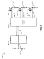
Referring now to FIG. 1, an exemplary MOSFET circuit 10 includes a smart or sense MOSFET 12, a control circuit 14, a gate resistor 16, and a current detection resistor 18. The MOSFET 12 includes at least a gate terminal 20, a source terminal 22, a drain terminal 24, and a current detection terminal 26. The gate terminal 20 is connected to an input voltage 28 through the gate resistor 16. The control circuit 14 senses a current through the current detection resistor 18. The current through the current detection resistor 18 is indicative of a current through the MOSFET 12. Therefore, the control circuit 14 determines the current through the MOSFET 12. For example, the control circuit 14 may determine when the current through the MOSFET 12 exceeds a particular threshold.
In certain implementations, the MOSFET 12 may include TEM (temperature) MOSFET functions. A TEM MOSFET includes one or more temperature detection terminals (not shown). The temperature detection terminals output a signal that is indicative of a temperature of the MOSFET 12. In this manner, the control circuit 14 may determine when the temperature of the MOSFET 12 exceeds a particular threshold.
Therefore, a MOSFET circuit according to the above embodiments relies on smart, sense, and/or TEM MOSFETs for current overload and/or over temperature protection. Smart, sense, and TEM MOSFETs require additional terminals to provide the current/temperature sensing functions, thereby increasing package size and cost. Further, the additional terminals reduce space available for bonding wires. Alternatively, a MOSFET circuit may include a power shunt resistor to sense a load current. However, in large current applications, the shunt resistor may generate significant heat, which is undesirable.
SUMMARY OF THE INVENTION
A sensorless protection circuit comprises a detection module. The detection module receives a reference voltage signal and receives a load voltage signal from a MOSFET. The detection module generates a detection signal having a first state and a second state according to the reference voltage signal and the load voltage signal. A protection module receives the detection signal and maintains the MOSFET in an ON state when the detection signal is in the first state and transitions the MOSFET from the ON state to an OFF state when the detection signal is in the second state. The detection signal is in the second state when the MOSFET is in at least one of a current overload condition, an over temperature condition, and a short circuit condition.
Further areas of applicability of the present invention will become apparent from the detailed description provided hereinafter. It should be understood that the detailed description and specific examples, while indicating the preferred embodiment of the invention, are intended for purposes of illustration only and are not intended to limit the scope of the invention.
BRIEF DESCRIPTION OF THE DRAWINGS
The present invention will become more fully understood from the detailed description and the accompanying drawings, wherein:
FIG. 1 is a circuit schematic of a MOSFET protection circuit that according to the prior art;
FIG. 2 is a functional block diagram of a sensorless MOSFET protection circuit according to the present invention;
FIG. 3A is a functional block diagram of a sensorless MOSFET protection circuit according to the present invention;
FIG. 3B is a table that illustrates status indications of the MOSFET protection circuit according to the present invention;
FIG. 4 is a functional block diagram of a sensorless MOSFET protection circuit including a trial interval timer according to the present invention;
FIG. 5 is a circuit schematic of a sensorless MOSFET protection circuit including a trial interval timer shown in more detail according to the present invention;
FIG. 6 is a waveform illustration of a retrial interval for a short circuit test according to the present invention;
FIG. 7 is a waveform illustration of MOSFET energy consumption during a short circuit condition according to the present invention; and
FIG. 8 is a functional block diagram of a sensorless MOSFET protection system according to the present invention.
DETAILED DESCRIPTION OF THE PREFERRED EMBODIMENTS
The following description of the preferred embodiments is merely exemplary in nature and is in no way intended to limit the invention, its application, or uses. For purposes of clarity, the same reference numbers will be used in the drawings to identify similar elements. As used herein, the term module and/or device refers to an application specific integrated circuit (ASIC), an electronic circuit, a processor (shared, dedicated, or group) and memory that execute one or more software or firmware programs, a combinational logic circuit, and/or other suitable components that provide the described functionality.
Referring now to FIG. 2, a sensorless MOSFET protection circuit 50 is shown. The protection circuit 50 includes a MOSFET 52, a MOSFET driver module 54, a detection module 56, and a protection module 58. The MOSFET 52 includes a gate terminal 60, a drain terminal 62, and a source terminal 64. Typically, certain characteristics of a MOSFET are temperature sensitive. For example, a voltage drop across the drain terminal 62 and the source terminal 64 is indicative of a load current at a particular temperature of the MOSFET 52. Similarly, a voltage drop across the drain terminal 62 and the source terminal 64 is indicative of a temperature of the MOSFET 52 at a particular load current. In other words, when certain characteristics of the MOSFET 52 are known, other characteristics, such as current and temperature, may be determined.
The source terminal 64 outputs a detection signal 66. The detection signal 66 is indicative of a temperature and/or a load current of the MOSFET 52. The detection module 56 receives the detection signal 66 and generates a detection output signal 68. For example, the detection output signal 68 is indicative of whether the detection signal 66 is above or below a threshold. When the detection signal 66 is above or below the threshold, the detection output signal 68 is indicative of a short circuit, current overload, and/or an over temperature condition. Additionally, the detection output signal 68 may be indicative of a startup inrush current condition. Similarly, the detection output signal 68 may be indicative of whether the detection signal 66 is within a range of values. When the detection signal 66 is within or outside the range of values, the detection output signal 68 is indicative of the short circuit, current overload, and/or over temperature condition.
The protection module 58 receives the detection output signal 68 and an input control signal 70. When the detection output signal 68 indicates a short circuit, current overload, and/or over temperature condition, the protection module 58 turns OFF the MOSFET 52. When the MOSFET 52 is ON, current flows from an power supply voltage (such as a battery voltage source) 72, through the MOSFET 52, to a load 74. As such, the detection signal 66 is indicative of a voltage of the load 74. When the MOSFET 52 is OFF, the MOSFET 52 prevents current flow to the load 74. When the protection module 58 turns OFF the MOSFET 52, the input control signal 70 is used to reset the protection module 58 and return the MOSFET 52 to an ON state.
Referring now to FIG. 3A, a first implementation of the sensorless MOSFET protection circuit 50 is shown in more detail. In addition to the elements described in FIG. 2, the protection circuit 50 may include a high voltage reference module 80 and a low voltage reference module 82. The high voltage reference module 80 and the low voltage reference module 82 receive the power supply voltage 72 and generate a high voltage reference signal 84 and a low voltage reference signal 86, respectively. In other words, the high voltage reference module 80 and the low voltage reference module 82 generate voltage reference signals that are referenced to the power supply voltage 72. For example, the high voltage reference signal 84 may be a difference between the power supply voltage 72 and 0.1 volts. Similarly, the low voltage reference signal 86 may be a difference between the power supply voltage 72 and 0.5 volts.
The detection module 56 includes a first comparator 88, a second comparator 90, and a detection module timer 92. The first comparator 88 receives the detection signal 66, the high voltage reference signal 84, and the power supply voltage 72. Similarly, the second comparator 90 receives the detection signal 66 and the low voltage reference signal 86. The detection module 56 further includes logic OR gates 94 and 96.
The protection module 58 includes an inrush current timer 98, logic AND gates 100 and 102, and a latch 104. The inrush current timer 98 receives a first detection module output signal 106 from the detection module 56 and generates an inrush current timer signal 108. The logic gate 100 receives the inrush current timer signal 108 and a second detection module output signal 110. The latch 104 receives a latch control signal 112 from the logic gate 100 and the input control signal 70. The logic gate 102 receives a latch output signal 114 from the latch 104 and the input control signal 70. The logic gate 102 outputs a MOSFET control signal 116.
Typically, a first comparator output signal 118 is HIGH. The first comparator output signal 118 is HIGH when the detection signal 66 is greater than the high voltage reference signal 84. When the detection signal 66 is less than the high voltage reference signal 84, the first comparator output signal 118 is LOW. Similarly, a second comparator output signal 120 is typically HIGH. The second comparator output signal 120 is HIGH when the detection signal 66 is greater than the low voltage reference signal 86. When the detection signal 66 is less than the low voltage reference signal 86, the second comparator output signal 120 is LOW.
In the present implementation, the detection signal 66 is greater than the high voltage reference signal 84 under normal operating conditions of the MOSFET 52 (i.e. when there is no short circuit, current overload, over temperature, and/or startup inrush current condition). The first comparator output signal 118 is HIGH. Likewise, the second comparator output signal 120 is HIGH.
When there MOSFET 52 is in a current overload, over temperature, and/or startup inrush current condition, the detection signal 66 is greater than the low voltage reference signal 86 but less than the high voltage reference signal 84. The first comparator output signal 118 is LOW and the second comparator output signal 120 is HIGH.
When the MOSFET 52 is in a short circuit condition, the detection signal 66 is less than the low voltage reference signal 86. The first comparator output signal 118 is LOW and the second comparator output signal 120 is LOW.
The MOSFET 52 is ON when the MOSFET control signal 116 is HIGH. Therefore, generally, the MOSFET 52 is ON when the first comparator output signal 118, the second comparator output signal 120, and the input control signal 70 are HIGH. As can be understood by the above description, the MOSFET 52 is ON when the detection signal 66 is greater than the high voltage reference signal 84, and is otherwise OFF.
The inrush current timer 98 maintains the MOSFET 52 in an ON state during startup inrush current conditions. In other words, the inrush current timer 98 prevents the protection module 58 from turning OFF the MOSFET 52 until after a startup inrush current time. During normal operating conditions (i.e. when the detection signal 66 is greater than the high voltage reference signal 84), the inrush current timer signal 108 is HIGH. When the first comparator output signal 118 transitions from HIGH to LOW, the first detection module output signal 106 transitions from HIGH to LOW and the inrush current timer 98 begins to count for a predetermined time. For example, the inrush current timer 98 may count to 0.5 seconds, 1.0 seconds, or other predetermined times. When the inrush current timer 98 reaches the predetermined time, the inrush current timer signal 108 transitions from HIGH to LOW. In this manner, the inrush current timer 98 turns OFF the MOSFET 52 when a current overload or over temperature condition occurs without triggering due to a temporary startup inrush current condition.
When at least one of the inrush current timer signal 108 and/or the second detection module output signal 110 is LOW, the latch control signal 112 transitions from HIGH to LOW, latching the latch output signal 114 in a LOW (i.e. OFF) state. In other words, the MOSFET 52 is turned OFF. In the present implementation, the input control signal 70 is toggled from HIGH to LOW and from LOW to HIGH to return the MOSFET 52 to an ON state.
Before the MOSFET 52 is initially turned ON, the detection signal 66 is at a ground potential 122 and the first and second comparator output signals 118 and 120 are LOW. The detection module timer 92 receives the detection signal 66 and outputs a detection module timer signal 124. When the load 74 is OFF (i.e. when the MOSFET 52 is OFF), the detection module timer signal 124 is HIGH. The logic OR gates 94 and 96 receive the detection module timer signal 124. Therefore, the HIGH state of the detection module timer signal 124 overcomes the initial LOW states of the first and second comparator output signals 118 and 120 and the MOSFET 52 can be turned ON. When the load 74 is turned ON, the detection module timer signal 124 transitions from HIGH to LOW, and the detection module 56 and protection module 58 can function to provide protection of the MOSFET 52 as described above. In other words, the protection functions are available when the load 74 is turned ON and are not available when the load 74 is turned OFF.
The protection circuit 50 may include a diode 126 and a zener diode 128. The diode 126 and the zener diode 128 form an active clamp circuit 130 for the MOSFET 52. The active clamp circuit 130 absorbs magnetic kickback during turn off periods for inductive loads.
Referring now to FIGS. 3A and 3B, statuses of the load 74 and the MOSFET 52 can be determined according to status signals 132 and 134 and/or the input control signal 70. When the MOSFET 52 is ON, the status signal 132 is HIGH. Conversely, the status signal 132 is LOW when the MOSFET 52 is OFF. When the load 74 is ON, the status signal 134 is LOW. Conversely, the status signal 134 is HIGH when the load 74 is OFF. Referring now to FIG. 3B, a table 140 illustrates diagnosis conditions of the protection circuit 50 according to the status signals 132 and 134 and/or the input control signal 70.
Referring now to FIG. 4, a second implementation of the sensorless MOSFET protection circuit 50 includes a trial interval timer 150, a latch 152, logic NAND gate 154, and logic AND gate 156. When a short circuit is detected (i.e. when the detection signal 66 is less than the low voltage reference signal 86), a timer input signal 158 (an output of the first logic AND gate 154) transitions from HIGH to LOW. A timer output signal 160 immediately transitions from HIGH to LOW to turn OFF the MOSFET 52. After a predetermined time, the timer output signal 160 transitions from LOW to HIGH. For example, the timer output signal 160 may transition from LOW to HIGH after 0.5 seconds or 1.0 seconds. In this manner, the trial interval timer 150 prevents the MOSFET 52 from being turned ON immediately after a short circuit condition. The trial interval timer 150 repeats the delayed cycle until after the MOSFET 52 is no longer in the short circuit condition.
Referring now to FIG. 5, the sensorless MOSFET protection circuit 50 as described in FIG. 4 is shown in more detail. In particular, the detection module timer 92, the inrush current timer 98, the trial interval timer 150, and the MOSFET driver module 50 are shown as detailed circuit schematics. Those skilled in the art can appreciate that any number of suitable components can replace those shown in FIG. 5. As such, the components shown in FIG. 5 are merely exemplary and the sensorless MOSFET protection circuit 50 is not to be limited to the presently illustrated embodiment.
Referring now to FIG. 6, behavior of the sensorless MOSFET protection circuit during a short circuit condition is illustrated. A first signal 170 illustrates voltage across the drain and source of the MOSFET. A second signal 172 illustrates current through the load. As shown, the trial interval timer outputs a LOW output signal when the first signal 170 indicates a short circuit condition. At a first time indicated at 174, the trial interval timer transitions the output signal from LOW to HIGH to determine whether the short circuit condition is still present, as indicated by a spike 176 in the second signal 172. In other words, the spike 176 indicates a short circuit trial that determines whether the short circuit condition is still present.
Because the first signal 170 continues to indicate a short circuit condition, the trial interval timer immediately transitions the output signal from HIGH to LOW. After a 1.0 second interval, the trial interval timer again transitions the output signal from LOW to HIGH at a second time indicated at 178 and by a spike 180. The trial interval timer again immediately transitions the output signal from HIGH to LOW. In this manner, it can be seen that the protection circuit described in FIGS. 2 through 5 is able to provide MOSFET protection without current and/or temperature sensors.
Referring now to FIG. 7, energy consumption of the MOSFET during a short circuit trial 190 is shown. A first signal 192 indicates a voltage across the drain and source of the MOSFET. A second signal 194 indicates a current through the load. A third signal 196 is a product of the first signal 192 and the second signal 194. In other words, the third signal 196 indicates energy consumption of the MOSFET during the short circuit trial 190. As shown the energy consumption of the MOSFET during the short circuit trial 190 is approximately 7.5 millijoules (mJ).
Referring now to FIG. 8, a sensorless MOSFET protection system 200 includes a multi-channel protection circuit 202 and a control module 204. The protection circuit 202 includes circuitry to implement a sensorless MOSFET protection circuit according to FIGS. 2 through 5. The protection circuit 202 receives detection signals 206-1, 206-2, . . . , and 206-n, referred to collectively as detection signals 206, from MOSFETs 208-1, 208-2, . . . , and 208-n, referred to collectively as MOSFETs 208. The MOSFETs 208 provide current to loads 210-1, 210-2, . . . , and 210-n, referred to collectively as loads 210.
A temperature sensor 212 such as a thermistor monitors ambient temperature. The control module 204 receives an ambient temperature signal 214 and dynamically programs the reference voltages (i.e. the high and low voltage references as described in FIGS. 2 through 5) for each of the MOSFETs 208 according to ambient temperature. For example, at high ambient temperatures, the high voltage reference may be programmed at a first value. At low ambient temperatures, the high voltage reference may be programmed at a second value that is greater than the first value. In this manner, the protection circuit 202 can be dynamically programmed to compensate for ambient temperature changes.
The control module 204 may communicate with the protection circuit 202 and program the voltage references through serial communication lines 216. Further, the control module 204 can send/receive the input control signal and/or receive the status signals through the serial communication lines 216.
The description of the invention is merely exemplary in nature and, thus, variations that do not depart from the gist of the invention are intended to be within the scope of the invention. Such variations are not to be regarded as a departure from the spirit and scope of the invention.

Claims (14)

1. A protection circuit comprising:
a detection module that receives a first reference voltage signal and receives a load voltage signal from a MOSFET, and that generates a detection signal having a first state and a second state according to the first reference voltage signal and the load voltage signal; and
a protection module that receives the detection signal and maintains the MOSFET in an ON state when the detection signal is in the first state and transitions the MOSFET from the ON state to an OFF state when the detection signal is in the second state,
wherein the MOSFET does not include a current sensor and does not include a temperature sensor, the detection signal is in the second state when the MOSFET is in at least one of a current overload condition and a short circuit condition, and the detection signal is in the second state when the MOSFET is in an over temperature condition.
2. The protection circuit of claim 1 further comprising a first reference voltage module that generates the first reference voltage signal.
3. The protection circuit of claim 2 further comprising a second reference voltage module that generates a second reference voltage signal that is less than the first reference voltage signal.
4. The protection circuit of claim 1 wherein the detection module includes a voltage comparator that receives the load voltage signal and the first reference voltage signal and that generates the detection signal, wherein the detection signal is in the first state when the load voltage signal is greater than the first reference voltage signal and the detection signal is in the second state when the load voltage signal is less than the first reference voltage signal.
5. The protection circuit of claim 1 wherein the detection signal is in the second state when the MOSFET is in at least one of the current overload condition and the short circuit condition, and the load voltage signal is above a threshold, and the detection signal is in the first state when the load voltage signal is below the threshold.
6. A protection circuit comprising:
a first reference voltage module that generates a first reference voltage signal;
a second reference voltage module that generates a second reference voltage signal that is less than the first reference voltage signal;
a detection module that includes a first voltage comparator that receives a load voltage signal from a MOSFET and the first reference voltage signal, a second voltage comparator that receives the load voltage signal and the second reference voltage signal, and that generates first and second detection signals having first and second states according to the first reference voltage signal, the second reference voltage signal, and the load voltage signal; and
a protection module that receives the first and second detection signals and maintains the MOSFET in an ON state when the detection signals are in the first state and transitions the MOSFET from the ON state to an OFF state when at least one of the detection signals is in the second state,
wherein the MOSFET does not include a current sensor and does not include a temperature sensor, and the first detection signal is in the second state when the load voltage signal is less than the first reference voltage signal and the second detection signal is in the second state when the load voltage signal is less than the second reference voltage signal.
7. The protection circuit of claim 6 wherein the load voltage signal is less than the first reference voltage signal when the MOSFET is in at least one of a current overload condition, a startup inrush current condition, and a short circuit condition, and is less than the first reference voltage signal when the MOSFET is in an over temperature condition.
8. The protection circuit of claim 6 wherein the load voltage signal is less than the second reference voltage signal when the MOSFET is in a short circuit condition.
9. The protection circuit of claim 6 wherein the detection module further comprises a detection module timer that receives the load voltage signal and that generates a detection module timer signal having first and second states and the detection module timer signal is in the first state when the load voltage signal is at a ground potential.
10. The protection circuit of claim 6 wherein the protection module includes a inrush current timer that maintains the MOSFET in the ON state when the first detection signal is in the second state for less than a first period and that transitions the MOSFET to the OFF state when the first detection signal is in the second state for greater than the first period.
11. The protection circuit of claim 6 wherein the protection module further comprises a trial interval timer that maintains the MOSFET in the OFF state for a first period when the second detection signal transitions from the first state to the second state.
12. The protection circuit of claim 11 wherein the trial interval timer transitions the MOSFET from the OFF state to the ON state after the first period.
13. The protection circuit of claim 9 wherein the load voltage signal is at the ground potential when a load connected to the protection circuit is OFF.
14. A protection system for a MOSFET, comprising:
at least one reference voltage module that generates at least one reference voltage signal;
a detection module that receives the reference voltage signal and receives a load voltage signal from a MOSFET, and that generates a detection signal having a first state and a second state according to the reference voltage signal and the load voltage signal;
a protection module that receives the detection signal and maintains the MOSFET in an ON state when the detection signal is in the first state and transitions the MOSFET from the ON state to an OFF state when the detection signal is in the second state; and
a control module that communicates with the reference voltage module and a temperature sensor, that receives a temperature signal from the temperature sensor, that determines a value of the reference voltage signal according to the temperature signal, and that programs the reference voltage module according to the value,
wherein the MOSFET does not include a current sensor and does not include a temperature sensor, the detection signal is in the second state when the MOSFET is in at least one of a current overload condition, a startup inrush current condition, and a short circuit condition, and the detection signal is in the second state when the MOSFET is in an over temperature condition.
US11/269,192 2005-11-08 2005-11-08 Protection circuit for digital power module Expired - Fee Related US7468874B1 (en)

Priority Applications (1)

Application Number Priority Date Filing Date Title
US11/269,192 US7468874B1 (en) 2005-11-08 2005-11-08 Protection circuit for digital power module

Applications Claiming Priority (1)

Application Number Priority Date Filing Date Title
US11/269,192 US7468874B1 (en) 2005-11-08 2005-11-08 Protection circuit for digital power module

Publications (1)

Publication Number Publication Date
US7468874B1 true US7468874B1 (en) 2008-12-23

Family

ID=40134254

Family Applications (1)

Application Number Title Priority Date Filing Date
US11/269,192 Expired - Fee Related US7468874B1 (en) 2005-11-08 2005-11-08 Protection circuit for digital power module

Country Status (1)

Country Link
US (1) US7468874B1 (en)

Cited By (10)

* Cited by examiner, † Cited by third party
Publication number Priority date Publication date Assignee Title
US20070247774A1 (en) * 2006-04-21 2007-10-25 Cheng Xiao-Chang Noise immune over current protection with inherent current limiting for switching power converter
US20090257159A1 (en) * 2008-04-09 2009-10-15 Kabushiki Kaisha Tokai Rika Denki Seisakusho Short circuit protection circuit
WO2012024160A1 (en) * 2010-08-18 2012-02-23 Snap-On Incorporated Overvoltage and overcurrent protection scheme
DE102010055479A1 (en) * 2010-12-22 2012-06-28 Continental Automotive Gmbh Smart FET controlling circuit for use in switching arrangement serving as electronic control unit in electronic system, has control circuit generating control signal that switches off switch during incorrect operation
CN103457236A (en) * 2013-07-04 2013-12-18 万能亿自动化科技(苏州)有限公司 Distribution box protection module
US20140184185A1 (en) * 2013-01-03 2014-07-03 Stmicroelectronics S.R.L. Electric system comprising a load driving apparatus by auto-recovery mode, and method of operating the apparatus
CN103944483A (en) * 2013-01-22 2014-07-23 株式会社牧田 Motor control circuit
US9620951B2 (en) 2011-02-18 2017-04-11 Nxp Usa, Inc. Overcurrent protection device and method of operating a power switch
CN108370155A (en) * 2015-12-25 2018-08-03 株式会社自动网络技术研究所 Power supply control apparatus
US10115503B2 (en) 2016-01-07 2018-10-30 Yazaki North America, Inc. Terminal-thermistor assembly

Citations (15)

* Cited by examiner, † Cited by third party
Publication number Priority date Publication date Assignee Title
US5497285A (en) 1993-09-14 1996-03-05 International Rectifier Corporation Power MOSFET with overcurrent and over-temperature protection
US5502610A (en) * 1993-09-02 1996-03-26 Micrel, Inc. Switching regulator having high current prevention features
US5550701A (en) 1994-08-30 1996-08-27 International Rectifier Corporation Power MOSFET with overcurrent and over-temperature protection and control circuit decoupled from body diode
US5737169A (en) * 1996-02-28 1998-04-07 Eni, A Division Of Astec America, Inc. Intrinsic element sensing integrated SOA protection for power MOSFET switches
US5747975A (en) 1994-03-22 1998-05-05 Sgs-Thomson Microelectronics S.R.L. Overload protection circuit for MOS power drivers
US5841649A (en) 1997-01-10 1998-11-24 Turbodyne Systems, Inc. Current-sensing mosfets in paralleled mosfet power circuit
US6043701A (en) 1996-07-18 2000-03-28 Siemens Aktiengesellschaft Circuit configuration for protecting a power MOSFET
US6137165A (en) 1999-06-25 2000-10-24 International Rectifier Corp. Hybrid package including a power MOSFET die and a control and protection circuit die with a smaller sense MOSFET
US20010009494A1 (en) 2000-01-26 2001-07-26 Shinichi Umekawa Over current protection circuit of semiconductor switching device
US6320275B1 (en) * 1998-07-03 2001-11-20 Hitachi, Ltd. Power-feed control apparatus provided in a vehicle
US6459167B1 (en) * 1999-02-26 2002-10-01 Yazaki Corporation System for controlling electromotive force of motor of electric vehicle
US6717787B2 (en) 2001-02-22 2004-04-06 Koninklijke Philips Electronics N.V. Current sensing IC with resistive sensing
US6914416B2 (en) * 1998-04-15 2005-07-05 Tyco Electronics Corporation Electrical device including a voltage regulator mounted on a variable resistor
US20060077606A1 (en) * 2004-09-29 2006-04-13 Denso Corporation Controller for semiconductor device
US7116110B1 (en) * 2005-06-30 2006-10-03 Yazaki North America, Inc. Sensorless protection for electronic device

Patent Citations (16)

* Cited by examiner, † Cited by third party
Publication number Priority date Publication date Assignee Title
US5502610A (en) * 1993-09-02 1996-03-26 Micrel, Inc. Switching regulator having high current prevention features
US5497285A (en) 1993-09-14 1996-03-05 International Rectifier Corporation Power MOSFET with overcurrent and over-temperature protection
US5747975A (en) 1994-03-22 1998-05-05 Sgs-Thomson Microelectronics S.R.L. Overload protection circuit for MOS power drivers
US5550701A (en) 1994-08-30 1996-08-27 International Rectifier Corporation Power MOSFET with overcurrent and over-temperature protection and control circuit decoupled from body diode
US5737169A (en) * 1996-02-28 1998-04-07 Eni, A Division Of Astec America, Inc. Intrinsic element sensing integrated SOA protection for power MOSFET switches
US6043701A (en) 1996-07-18 2000-03-28 Siemens Aktiengesellschaft Circuit configuration for protecting a power MOSFET
US5841649A (en) 1997-01-10 1998-11-24 Turbodyne Systems, Inc. Current-sensing mosfets in paralleled mosfet power circuit
US6914416B2 (en) * 1998-04-15 2005-07-05 Tyco Electronics Corporation Electrical device including a voltage regulator mounted on a variable resistor
US6320275B1 (en) * 1998-07-03 2001-11-20 Hitachi, Ltd. Power-feed control apparatus provided in a vehicle
US6459167B1 (en) * 1999-02-26 2002-10-01 Yazaki Corporation System for controlling electromotive force of motor of electric vehicle
US6137165A (en) 1999-06-25 2000-10-24 International Rectifier Corp. Hybrid package including a power MOSFET die and a control and protection circuit die with a smaller sense MOSFET
US6300146B1 (en) 1999-06-25 2001-10-09 International Rectifier Corp. Hybrid package including a power MOSFET die and a control and protection circuit die with a smaller sense MOSFET
US20010009494A1 (en) 2000-01-26 2001-07-26 Shinichi Umekawa Over current protection circuit of semiconductor switching device
US6717787B2 (en) 2001-02-22 2004-04-06 Koninklijke Philips Electronics N.V. Current sensing IC with resistive sensing
US20060077606A1 (en) * 2004-09-29 2006-04-13 Denso Corporation Controller for semiconductor device
US7116110B1 (en) * 2005-06-30 2006-10-03 Yazaki North America, Inc. Sensorless protection for electronic device

Non-Patent Citations (1)

* Cited by examiner, † Cited by third party
Title
BUK3F00-50WEHL TrenchPLUS controller 1C (Rev. 01-Nov. 1, 2004).

Cited By (15)

* Cited by examiner, † Cited by third party
Publication number Priority date Publication date Assignee Title
US7636227B2 (en) * 2006-04-21 2009-12-22 International Rectifier Corporation Noise immune over current protection with inherent current limiting for switching power converter
US20070247774A1 (en) * 2006-04-21 2007-10-25 Cheng Xiao-Chang Noise immune over current protection with inherent current limiting for switching power converter
US8139333B2 (en) * 2008-04-09 2012-03-20 Kabushiki Kaisha Tokai Rika Denki Seisakusho Short circuit protection circuit
US20090257159A1 (en) * 2008-04-09 2009-10-15 Kabushiki Kaisha Tokai Rika Denki Seisakusho Short circuit protection circuit
US8390974B2 (en) 2010-08-18 2013-03-05 Snap-On Incorporated Overvoltage and overcurrent protection scheme
WO2012024160A1 (en) * 2010-08-18 2012-02-23 Snap-On Incorporated Overvoltage and overcurrent protection scheme
DE102010055479A1 (en) * 2010-12-22 2012-06-28 Continental Automotive Gmbh Smart FET controlling circuit for use in switching arrangement serving as electronic control unit in electronic system, has control circuit generating control signal that switches off switch during incorrect operation
US9620951B2 (en) 2011-02-18 2017-04-11 Nxp Usa, Inc. Overcurrent protection device and method of operating a power switch
US20140184185A1 (en) * 2013-01-03 2014-07-03 Stmicroelectronics S.R.L. Electric system comprising a load driving apparatus by auto-recovery mode, and method of operating the apparatus
US9436193B2 (en) * 2013-01-03 2016-09-06 Stmicroelectronics S.R.L. Electric system comprising a load driving apparatus by auto-recovery mode, and method of operating the apparatus
CN103944483A (en) * 2013-01-22 2014-07-23 株式会社牧田 Motor control circuit
CN103457236A (en) * 2013-07-04 2013-12-18 万能亿自动化科技(苏州)有限公司 Distribution box protection module
CN103457236B (en) * 2013-07-04 2016-03-23 基元电气有限公司 A kind of distribution box protection module
CN108370155A (en) * 2015-12-25 2018-08-03 株式会社自动网络技术研究所 Power supply control apparatus
US10115503B2 (en) 2016-01-07 2018-10-30 Yazaki North America, Inc. Terminal-thermistor assembly

Similar Documents

Publication Publication Date Title
US7468874B1 (en) Protection circuit for digital power module
US11289894B2 (en) Overcurrent protection circuit
US11239837B2 (en) Switch device
US10044180B2 (en) Electronic circuit breaker for an electrical load in an on-board electrical system of a motor vehicle
US7345383B2 (en) Abnormality detection apparatus for a power feed circuit
JP6478789B2 (en) Semiconductor device, power control semiconductor device, vehicle-mounted electronic control unit, and vehicle including the same
US7079368B2 (en) Electrical resource device and load driving device
US7847702B2 (en) Power supply controller
US8054602B2 (en) Power supply controller
CN107872212B (en) Control method, power switch device and switch device
US7977999B2 (en) Temperature detection circuit
JP2003209922A (en) Switching apparatus
US10985744B2 (en) Apparatus with integrated protection profile and method
JP2007082374A (en) Protection circuit on reverse connection of power supply
JP3587300B2 (en) Integrated circuit device
CN109477862B (en) Vehicle-mounted control device
US10088882B2 (en) Electronic control unit having multiple power supply routes for microcomputer core
US11329474B2 (en) Switching controller with adaptive overheating protection
US20140184185A1 (en) Electric system comprising a load driving apparatus by auto-recovery mode, and method of operating the apparatus
JP4736569B2 (en) Inductive load abnormality detection device
US7907376B2 (en) Load control device and method
CN110663156A (en) Input circuit capable of reducing dark current
JP2017073657A (en) Erroneous output prevention circuit
EP0954079A1 (en) Bidirectional electronic switch
KR20180112699A (en) Device and method for providing an activation voltage for a safety unit for a vehicle, and safety device

Legal Events

Date Code Title Description
AS Assignment

Owner name: YAZAKI NORTH AMERICA, INC., MICHIGAN

Free format text: ASSIGNMENT OF ASSIGNORS INTEREST;ASSIGNOR:GUO, SAM YONGHON;REEL/FRAME:017229/0497

Effective date: 20051013

AS Assignment

Owner name: YAZAKI NORTH AMERICA, INC., MICHIGAN

Free format text: CORRECTIVE ASSIGNMENT TO CORRECT THE EXECUTION DATE, PREVIOUSLY RECORDED AT REEL 017229, FRAME 0497;ASSIGNOR:GUO, SAM YONGHON;REEL/FRAME:017722/0164

Effective date: 20051031

REMI Maintenance fee reminder mailed
LAPS Lapse for failure to pay maintenance fees
STCH Information on status: patent discontinuation

Free format text: PATENT EXPIRED DUE TO NONPAYMENT OF MAINTENANCE FEES UNDER 37 CFR 1.362

FP Lapsed due to failure to pay maintenance fee

Effective date: 20121223