US7468898B2 - DC-DC converter with switchable capacitors - Google Patents
DC-DC converter with switchable capacitors Download PDFInfo
- Publication number
- US7468898B2 US7468898B2 US11/191,242 US19124205A US7468898B2 US 7468898 B2 US7468898 B2 US 7468898B2 US 19124205 A US19124205 A US 19124205A US 7468898 B2 US7468898 B2 US 7468898B2
- Authority
- US
- United States
- Prior art keywords
- capacitor
- phase
- converter
- capacitors
- output
- Prior art date
- Legal status (The legal status is an assumption and is not a legal conclusion. Google has not performed a legal analysis and makes no representation as to the accuracy of the status listed.)
- Expired - Fee Related
Links
Images


Classifications
-
- H—ELECTRICITY
- H02—GENERATION; CONVERSION OR DISTRIBUTION OF ELECTRIC POWER
- H02M—APPARATUS FOR CONVERSION BETWEEN AC AND AC, BETWEEN AC AND DC, OR BETWEEN DC AND DC, AND FOR USE WITH MAINS OR SIMILAR POWER SUPPLY SYSTEMS; CONVERSION OF DC OR AC INPUT POWER INTO SURGE OUTPUT POWER; CONTROL OR REGULATION THEREOF
- H02M3/00—Conversion of dc power input into dc power output
- H02M3/02—Conversion of dc power input into dc power output without intermediate conversion into ac
- H02M3/04—Conversion of dc power input into dc power output without intermediate conversion into ac by static converters
- H02M3/06—Conversion of dc power input into dc power output without intermediate conversion into ac by static converters using resistors or capacitors, e.g. potential divider
- H02M3/07—Conversion of dc power input into dc power output without intermediate conversion into ac by static converters using resistors or capacitors, e.g. potential divider using capacitors charged and discharged alternately by semiconductor devices with control electrode, e.g. charge pumps
- H02M3/072—Conversion of dc power input into dc power output without intermediate conversion into ac by static converters using resistors or capacitors, e.g. potential divider using capacitors charged and discharged alternately by semiconductor devices with control electrode, e.g. charge pumps adapted to generate an output voltage whose value is lower than the input voltage
Definitions
- This invention relates to a DC-DC converter, specifically to a DC-DC converter having a function to step down an input voltage.
- DC-DC converters are circuits that change a certain DC input voltage into another DC voltage, and are used in a power supply circuit of an LSI and the like.
- a step-down DC-DC converter that has a function to step down an input voltage is well known.
- C 1 -Cn are n capacitors switchable between a series connection and a parallel connection.
- Cout is an output capacitor (smoothing capacitor).
- the DC-DC converter is structured so that the n capacitors C 1 -Cn can be alternated by a switching circuit (not shown) between a status of series connection as shown in FIG. 4A and a status of parallel connection as shown in FIG. 4B .
- the status shown in FIG. 4A is called phase 1 and the status shown in FIG. 4B is called phase 2 hereafter. All the capacitors C 1 -Cn have the same capacitance.
- the capacitors C 1 -Cn are connected in series between an input voltage Vin (DC voltage) and a ground voltage Vss (0V) in the phase 1 .
- Vin DC voltage
- Vss ground voltage
- the capacitors C 1 -Cn are charged with electric charges corresponding to a voltage (1/n) ⁇ Vin that is Vin multiplied by 1/n.
- the capacitors C 1 -Cn are connected in parallel between the ground voltage Vss (0V) and an output terminal to which electric charges stored in the capacitors C 1 -Cn are discharged.
- the DC-DC converter described above requires n capacitors in order to multiply the input voltage Vin by 1/n, causing a problem of increased cost.
- This invention offers a DC-DC converter including (n ⁇ 1) capacitors switchable between a series connection and a parallel connection and outputs an output voltage Vout, that is an input voltage Vin multiplied by 1/n, with less number of capacitors than conventional DC-DC converters, by alternating between a status in which the (n ⁇ 1) capacitors are connected in parallel between an output terminal and a ground voltage and a status in which the (n ⁇ 1) capacitors are connected in series between an input voltage Vin and the output terminal.
- FIGS. 1A and 1B are circuit diagrams showing a first example of operation of a DC-DC converter according to an embodiment of this invention.
- FIGS. 2A and 2B are circuit diagrams showing a second example of operation of the DC-DC converter according to the embodiment of this invention.
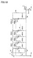
- FIG. 3 shows switching in the operation of the DC-DC converter according to the embodiment of this invention.
- FIGS. 4A and 4B are circuit diagrams showing a DC-DC converter according to a conventional art.
- FIGS. 1A , 1 B, 2 A and 2 B are circuit diagrams showing the DC-DC converter.
- FIGS. 1A and 1B are to explain a structure and an operation of a circuit that steps down an input voltage Vin to 1/n times of Vin.
- FIGS. 2A and 2B are to explain a structure and an operation of a circuit that steps down the input voltage Vin to (n ⁇ 1)/n times of Vin.
- the n is a natural number larger than one.
- the circuit shown in FIGS. 1A and 1B has the same circuit structure as the circuit shown in FIGS. 2A and 2B . Difference between them is only in a way of switching.
- C 1 -Cn- 1 are (n ⁇ 1) capacitors switchable between a series connection and a parallel connection by the operation of switches SWA 1 -SWAn- 1 , SWB 1 -SWBn- 2 and SWC 1 -SWCn- 2 .
- the capacitors C 1 -Cn- 1 are connected in parallel with each other when the switches SWA 1 -SWAn- 1 and SWC 1 -SWCn- 2 are turned on while the switches SWB 1 -SWBn- 2 are turned off.
- the capacitors C 1 -Cn- 1 are connected in series with each other when the switches SWAn- 1 and SWB 1 -SWBn- 2 are turned on while the switches SWA 1 -SWAn- 2 and SWC 1 -SWCn- 2 are turned off.
- Capacitances of the capacitors C 1 -Cn- 1 may be of any values. All of them may be of the same value. Or, at least one of the capacitors may have a capacitance different from the capacitance of the rest of the capacitors. That is, all the capacitances of the capacitors C 1 -Cn- 1 may be different from each other, or some of the capacitances may be the same while the rest of the capacitances are different.
- S 1 is a switch provided between an input terminal 1 to which the input voltage Vin is applied and one end of the capacitor C 1
- S 2 is a switch provided between the input terminal 1 and the other end of the capacitor C 1
- S 3 is a switch provided between the one end of the capacitor C 1 and a ground voltage Vss (0V)
- S 4 is a switch provided between the other end of the capacitor C 1 and the ground voltage Vss
- S 5 is a switch provided between the switch SWCn- 2 and an output terminal 2 from which an output voltage Vout is obtained
- S 6 is a switch provided between the switch SWAn- 1 and the output terminal 2
- Cout is an output capacitor (smoothing capacitor) connected between the output terminal 2 and the ground voltage Vss. All the switches can be formed of MOS transistors.
- FIG. 3 shows switching in the operation of the DC-DC converter.
- the symbol “0” in FIG. 3 denotes that the switch is turned on, and the symbol “X” denotes that the switch is turned off.
- the status shown in FIG. 1A is called phase 1 and the status shown in FIG. 1B is called phase 2 hereafter.
- Each of arrows in FIGS. 1A and 1B shows a direction of an electric current.
- the switches SWA 1 -SWAn- 1 and the switches SWC 1 -SWCn- 2 are turned on while the switches SWB 1 -SWBn- 2 are turned off, as shown in FIG. 3 .
- the switches S 4 and S 5 are turned on, while the switches S 1 , S 2 , S 3 and S 6 are turned off.
- (n ⁇ 1) capacitors C 1 -Cn- 1 are connected in parallel with each other and connected between the output terminal 2 and the ground voltage Vss.
- electric charges corresponding to the output voltage Vout are discharged from the output capacitor Cout, and electric charges corresponding to the output voltage Vout are charged to each of the capacitors C 1 -Cn- 1 .
- the switches SWAn- 1 and SWB 1 -SWBn- 2 are turned on while the switches SWA 1 -SWAn- 2 and the switches SWC 1 -SWCn- 2 are turned off, as shown in FIG. 3 .
- the switches S 1 and S 6 are turned on, while the switches, S 2 , S 3 , S 4 and S 5 are turned off.
- the capacitors C 1 -Cn- 1 are connected in series with each other and connected between the input voltage Vin (that is, the input terminal 1 to which the input voltage Vin is applied) and the output voltage Vout.
- the number of the alternation between the phase 1 and the phase 2 is about 8000.
- FIGS. 2A , 2 B and 3 a second example of operation of the DC-DC converter having the structure described above will be explained referring to FIGS. 2A , 2 B and 3 .
- all the capacitors C 1 -Cn- 1 have the same capacitance.
- the status shown in FIG. 2A is called phase 1 and the status shown in FIG. 2B is called phase 2 hereafter.
- Each of arrows in FIGS. 2A and 2B shows a direction of an electric current.
- the switches SWAn- 1 and SWB 1 -SWBn- 2 are turned on while the switches SWA 1 -SWAn- 2 and the switches SWC 1 -SWCn- 2 are turned off, as shown in FIG. 3 .
- the switches S 3 and S 6 are turned on, while the switches, S 1 , S 2 , S 4 and S 5 are turned off.
- the capacitors C 1 -Cn- 1 are connected in series with each other and connected between the output voltage Vout and the ground voltage Vss.
- electric charges corresponding to the output voltage Vout are discharged from the output capacitor Cout, and electric charges corresponding to a voltage Vout/(n- 1 ) are charged to each of the capacitors C 1 -Cn- 1 .
- the switches SWA 1 -SWAn- 1 and the switches SWC 1 -SWCn- 2 are turned on while the switches SWB 1 -SWBn- 2 are turned off, as shown in FIG. 3 .
- the switches S 2 and S 5 are turned on, while the switches S 1 , S 3 , S 4 and S 6 are turned off.
- the capacitors C 1 -Cn- 1 are connected in parallel with each other and connected between the input voltage Vin and the output voltage Vout.
- electric charges corresponding to the output voltage Vout are charged to the output capacitor Cout, and electric charges corresponding to a voltage Vin ⁇ Vout(n ⁇ 1) are discharged from each of the capacitors C 1 -Cn- 1 .
- the number of the alternation between the phase 1 and the phase 2 is about 8000.
- the input voltage Vin can be stepped down to 1/n times of Vin using (n ⁇ 1) capacitors, according to the DC-DC converter of this invention. That is, the number of capacitors can be reduced by one compared with the conventional DC-DC converter, enabling reduction in the cost of the DC-DC converter. Also, the input voltage Vin can be stepped down to (n ⁇ 1)/n times of Vin using (n ⁇ 1) capacitors, according to the DC-DC converter of this invention.
Abstract
Description
Vin−Vout·(n−1)=Vout
Vin−Vout·(n−1)= Vout
Claims (12)
Applications Claiming Priority (2)
| Application Number | Priority Date | Filing Date | Title |
|---|---|---|---|
| JP2004-221437 | 2004-07-29 | ||
| JP2004221437 | 2004-07-29 |
Publications (2)
| Publication Number | Publication Date |
|---|---|
| US20060028849A1 US20060028849A1 (en) | 2006-02-09 |
| US7468898B2 true US7468898B2 (en) | 2008-12-23 |
Family
ID=35757190
Family Applications (1)
| Application Number | Title | Priority Date | Filing Date |
|---|---|---|---|
| US11/191,242 Expired - Fee Related US7468898B2 (en) | 2004-07-29 | 2005-07-28 | DC-DC converter with switchable capacitors |
Country Status (4)
| Country | Link |
|---|---|
| US (1) | US7468898B2 (en) |
| KR (1) | KR100682006B1 (en) |
| CN (1) | CN1728518A (en) |
| TW (1) | TWI298970B (en) |
Cited By (10)
| Publication number | Priority date | Publication date | Assignee | Title |
|---|---|---|---|---|
| US20080157857A1 (en) * | 2006-12-27 | 2008-07-03 | Nec Electronics Corporation | Booster circuit |
| US20090256626A1 (en) * | 2008-04-14 | 2009-10-15 | Novatek Microelectronics Corp. | Multi-step charge pump and method for producing multi-step charge pumping |
| US20110050326A1 (en) * | 2009-08-28 | 2011-03-03 | Cook Thomas D | Charge pump with charge feedback and method of operation |
| US20110115549A1 (en) * | 2009-11-16 | 2011-05-19 | Cook Thomas D | Charge pump for use with a synchronous load |
| US7965130B1 (en) | 2009-12-08 | 2011-06-21 | Freescale Semiconductor, Inc. | Low power charge pump and method of operation |
| US20140328101A1 (en) * | 2011-11-28 | 2014-11-06 | Omron Corporation | Voltage conversion circuit and electronic apparatus |
| US20180269700A1 (en) * | 2016-02-05 | 2018-09-20 | Guangdong Oppo Mobile Telecommunications Corp., Ltd. | Adapter and method of controlling charging process |
| CN109120024A (en) * | 2017-06-22 | 2019-01-01 | 立锜科技股份有限公司 | Charging unit with multiple power source path |
| US10293702B2 (en) | 2013-06-17 | 2019-05-21 | Mcmaster University | Reconfigurable hybrid energy storage system for electrified vehicles |
| US10715037B2 (en) | 2016-08-05 | 2020-07-14 | The University Of Hong Kong | High-efficiency switched-capacitor power supplies and methods |
Families Citing this family (18)
| Publication number | Priority date | Publication date | Assignee | Title |
|---|---|---|---|---|
| GB2447426B (en) * | 2006-12-22 | 2011-07-13 | Wolfson Microelectronics Plc | Charge pump circuit and methods of operation thereof |
| GB2444984B (en) * | 2006-12-22 | 2011-07-13 | Wolfson Microelectronics Plc | Charge pump circuit and methods of operation thereof |
| EP2043243A1 (en) * | 2007-09-27 | 2009-04-01 | ABB Schweiz AG | Converter switching mechanism and method for operating such a converter switching mechanism |
| WO2009136368A1 (en) * | 2008-05-09 | 2009-11-12 | Nxp B.V. | Charge pump dc-dc converter |
| CN101453162B (en) * | 2008-09-16 | 2012-04-25 | 北京交通大学 | Topology structure for T type boosting converter |
| EP2244364A1 (en) * | 2009-04-23 | 2010-10-27 | Mitsubishi Electric R&D Centre Europe B.V. | Method and an apparatus for controlling the switches of a boost converter composed of plural bridge devices |
| JP5310662B2 (en) * | 2010-07-02 | 2013-10-09 | オムロン株式会社 | Voltage conversion circuit and electronic device |
| KR101315143B1 (en) * | 2012-08-22 | 2013-10-14 | 전북대학교산학협력단 | High efficiency dc/dc power converter with high conversion ratio |
| US8619445B1 (en) | 2013-03-15 | 2013-12-31 | Arctic Sand Technologies, Inc. | Protection of switched capacitor power converter |
| US10693368B2 (en) | 2014-03-14 | 2020-06-23 | Psemi Corporation | Charge pump stability control |
| KR102320321B1 (en) * | 2014-03-14 | 2021-11-01 | 아크틱 샌드 테크놀로지스, 인크. | Charge pump stability control |
| CN104218802A (en) * | 2014-09-26 | 2014-12-17 | 三峡大学 | Non-isolated high-voltage-reduction-ratio DC/DC convertor |
| CN105226979B (en) * | 2015-10-22 | 2017-11-21 | 北京京仪椿树整流器有限责任公司 | A kind of level circuits of modified L Boost tetra- |
| CN106130372B (en) * | 2016-07-21 | 2018-07-03 | 唐山东唐电气股份有限公司 | Alternating current is without change booster power |
| KR102553587B1 (en) | 2018-02-22 | 2023-07-10 | 삼성전자 주식회사 | Power converter and method for converting power |
| CN109586371A (en) * | 2018-12-13 | 2019-04-05 | 上海交通大学 | The series-parallel suitching type battery circuit of charge and discharge |
| KR102355293B1 (en) * | 2019-09-27 | 2022-01-25 | 주식회사 실리콘마이터스 | Switched-capacitor converter |
| US11502619B1 (en) * | 2021-07-30 | 2022-11-15 | Texas Instruments Incorporated | Hybrid multi-level inverter and charge pump |
Citations (8)
| Publication number | Priority date | Publication date | Assignee | Title |
|---|---|---|---|---|
| US4451743A (en) * | 1980-12-29 | 1984-05-29 | Citizen Watch Company Limited | DC-to-DC Voltage converter |
| US4531113A (en) * | 1983-06-27 | 1985-07-23 | Gte Laboratories Incorporated | Capacitor array |
| US5434569A (en) * | 1993-09-01 | 1995-07-18 | Texas Instruments Incorporated | Methods for adjusting the coupling capacitor of a multi-stage weighted capacitor A/D converter |
| US5581454A (en) * | 1994-11-22 | 1996-12-03 | Collins; Hansel | High power switched capacitor voltage conversion and regulation apparatus |
| JPH09163719A (en) | 1995-11-30 | 1997-06-20 | Fujitsu Ltd | Stepdown circuit |
| US6198645B1 (en) * | 1998-07-02 | 2001-03-06 | National Semiconductor Corporation | Buck and boost switched capacitor gain stage with optional shared rest state |
| JP2003111385A (en) | 2001-09-26 | 2003-04-11 | Sanyo Electric Co Ltd | Dc-dc converter |
| US6985024B2 (en) * | 2003-08-21 | 2006-01-10 | Analog Devices, Inc. | Voltage multiplier |
-
2005
- 2005-07-11 TW TW094123334A patent/TWI298970B/en not_active IP Right Cessation
- 2005-07-28 KR KR1020050068726A patent/KR100682006B1/en not_active IP Right Cessation
- 2005-07-28 US US11/191,242 patent/US7468898B2/en not_active Expired - Fee Related
- 2005-07-29 CN CNA2005100884342A patent/CN1728518A/en active Pending
Patent Citations (9)
| Publication number | Priority date | Publication date | Assignee | Title |
|---|---|---|---|---|
| US4451743A (en) * | 1980-12-29 | 1984-05-29 | Citizen Watch Company Limited | DC-to-DC Voltage converter |
| US4531113A (en) * | 1983-06-27 | 1985-07-23 | Gte Laboratories Incorporated | Capacitor array |
| US5434569A (en) * | 1993-09-01 | 1995-07-18 | Texas Instruments Incorporated | Methods for adjusting the coupling capacitor of a multi-stage weighted capacitor A/D converter |
| US5581454A (en) * | 1994-11-22 | 1996-12-03 | Collins; Hansel | High power switched capacitor voltage conversion and regulation apparatus |
| JPH09163719A (en) | 1995-11-30 | 1997-06-20 | Fujitsu Ltd | Stepdown circuit |
| US6198645B1 (en) * | 1998-07-02 | 2001-03-06 | National Semiconductor Corporation | Buck and boost switched capacitor gain stage with optional shared rest state |
| JP2003111385A (en) | 2001-09-26 | 2003-04-11 | Sanyo Electric Co Ltd | Dc-dc converter |
| US6834001B2 (en) | 2001-09-26 | 2004-12-21 | Sanyo Electric Co., Ltd. | Multi-stage switched capacitor DC-DC converter |
| US6985024B2 (en) * | 2003-08-21 | 2006-01-10 | Analog Devices, Inc. | Voltage multiplier |
Cited By (16)
| Publication number | Priority date | Publication date | Assignee | Title |
|---|---|---|---|---|
| US20080157857A1 (en) * | 2006-12-27 | 2008-07-03 | Nec Electronics Corporation | Booster circuit |
| US7663427B2 (en) * | 2006-12-27 | 2010-02-16 | Nec Electronics Corporation | Booster circuit |
| US20090256626A1 (en) * | 2008-04-14 | 2009-10-15 | Novatek Microelectronics Corp. | Multi-step charge pump and method for producing multi-step charge pumping |
| US8742832B2 (en) * | 2008-04-14 | 2014-06-03 | Novatek Microelectronics Corp. | Multi-step charge pump and method for producing multi-step charge pumping |
| US20110050326A1 (en) * | 2009-08-28 | 2011-03-03 | Cook Thomas D | Charge pump with charge feedback and method of operation |
| US7948301B2 (en) * | 2009-08-28 | 2011-05-24 | Freescale Semiconductor, Inc. | Charge pump with charge feedback and method of operation |
| US20110115549A1 (en) * | 2009-11-16 | 2011-05-19 | Cook Thomas D | Charge pump for use with a synchronous load |
| US7965130B1 (en) | 2009-12-08 | 2011-06-21 | Freescale Semiconductor, Inc. | Low power charge pump and method of operation |
| US20140328101A1 (en) * | 2011-11-28 | 2014-11-06 | Omron Corporation | Voltage conversion circuit and electronic apparatus |
| US9507370B2 (en) * | 2011-11-28 | 2016-11-29 | Omron Corporation | Voltage conversion circuit with improved conversion efficiency |
| US10293702B2 (en) | 2013-06-17 | 2019-05-21 | Mcmaster University | Reconfigurable hybrid energy storage system for electrified vehicles |
| US20180269700A1 (en) * | 2016-02-05 | 2018-09-20 | Guangdong Oppo Mobile Telecommunications Corp., Ltd. | Adapter and method of controlling charging process |
| US10985595B2 (en) * | 2016-02-05 | 2021-04-20 | Guangdong Oppo Mobile Telecommunications Corp., Ltd. | Adapter and method of controlling charging process |
| US10715037B2 (en) | 2016-08-05 | 2020-07-14 | The University Of Hong Kong | High-efficiency switched-capacitor power supplies and methods |
| CN109120024A (en) * | 2017-06-22 | 2019-01-01 | 立锜科技股份有限公司 | Charging unit with multiple power source path |
| CN109120024B (en) * | 2017-06-22 | 2020-06-30 | 立锜科技股份有限公司 | Charging device with multiple power supply paths |
Also Published As
| Publication number | Publication date |
|---|---|
| KR100682006B1 (en) | 2007-02-15 |
| TWI298970B (en) | 2008-07-11 |
| CN1728518A (en) | 2006-02-01 |
| KR20060048837A (en) | 2006-05-18 |
| TW200620796A (en) | 2006-06-16 |
| US20060028849A1 (en) | 2006-02-09 |
Similar Documents
| Publication | Publication Date | Title |
|---|---|---|
| US7468898B2 (en) | DC-DC converter with switchable capacitors | |
| US8295064B2 (en) | Operation control method of charge pump circuit | |
| US6563235B1 (en) | Switched capacitor array circuit for use in DC-DC converter and method | |
| KR100516083B1 (en) | Dc-dc converter | |
| EP3425784B1 (en) | Dc-dc converter with modular stages | |
| JP2006067783A (en) | Dc-dc converter | |
| US20200350821A1 (en) | Hybrid DC-DC Power Converter with Small Voltage Conversion Ratio | |
| US9331578B2 (en) | Multi-phase buck DC converter | |
| WO2006043479A1 (en) | Switching power supply and electronic apparatus employing the same | |
| US11671015B2 (en) | Three-level boost circuit and multiple-output parallel system | |
| EP2244368A1 (en) | Method and an apparatus for controlling the output voltage of a boost converter composed of plural bridge devices | |
| US20090219078A1 (en) | Charge pump down circuit and method for the same | |
| EP2846448A1 (en) | Switched capacitor power converter | |
| US8742832B2 (en) | Multi-step charge pump and method for producing multi-step charge pumping | |
| Chen et al. | A 92.7%-efficiency 30A 48V-to-1V dual-path hybrid Dickson converter for PoL applications | |
| CN112821757A (en) | Power converter | |
| WO2017195592A1 (en) | Power converter unit | |
| JPH08205524A (en) | Voltage converter | |
| JP2007259534A (en) | Semiconductor integrated circuit device, charge pump circuit, electrical equipment | |
| JP4837023B2 (en) | DC / DC power converter | |
| JPH10215564A (en) | Charge pump type dc-dc converter | |
| CN111030446B (en) | DC-DC/DC conversion topology circuit and device | |
| CN209982337U (en) | Three-level Boost circuit and multi-output parallel system | |
| US6727605B1 (en) | Duty cycle phase number control of polyphase interleaved converters | |
| CN113206595B (en) | Switching type power supply conversion circuit and switching circuit |
Legal Events
| Date | Code | Title | Description |
|---|---|---|---|
| AS | Assignment |
Owner name: SANYO ELECTRIC CO., LTD., JAPAN Free format text: ASSIGNMENT OF ASSIGNORS INTEREST;ASSIGNORS:OGATA, TAKASHIGE;SUZUKI, TATSUYA;REEL/FRAME:017130/0794 Effective date: 20051004 |
|
| STCF | Information on status: patent grant |
Free format text: PATENTED CASE |
|
| FEPP | Fee payment procedure |
Free format text: PAYOR NUMBER ASSIGNED (ORIGINAL EVENT CODE: ASPN); ENTITY STATUS OF PATENT OWNER: LARGE ENTITY |
|
| FEPP | Fee payment procedure |
Free format text: PAYER NUMBER DE-ASSIGNED (ORIGINAL EVENT CODE: RMPN); ENTITY STATUS OF PATENT OWNER: LARGE ENTITY Free format text: PAYOR NUMBER ASSIGNED (ORIGINAL EVENT CODE: ASPN); ENTITY STATUS OF PATENT OWNER: LARGE ENTITY |
|
| AS | Assignment |
Owner name: SEMICONDUCTOR COMPONENTS INDUSTRIES, LLC, ARIZONA Free format text: ASSIGNMENT OF ASSIGNORS INTEREST;ASSIGNOR:SANYO ELECTRIC CO., LTD.;REEL/FRAME:026594/0385 Effective date: 20110101 |
|
| FPAY | Fee payment |
Year of fee payment: 4 |
|
| AS | Assignment |
Owner name: SEMICONDUCTOR COMPONENTS INDUSTRIES, LLC, ARIZONA Free format text: CORRECTIVE ASSIGNMENT TO CORRECT THE INCORRECT #12/577882 PREVIOUSLY RECORDED ON REEL 026594 FRAME 0385. ASSIGNOR(S) HEREBY CONFIRMS THE ASSIGNMENT;ASSIGNOR:SANYO ELECTRIC CO., LTD;REEL/FRAME:032836/0342 Effective date: 20110101 |
|
| AS | Assignment |
Owner name: DEUTSCHE BANK AG NEW YORK BRANCH, NEW YORK Free format text: SECURITY INTEREST;ASSIGNOR:SEMICONDUCTOR COMPONENTS INDUSTRIES, LLC;REEL/FRAME:038620/0087 Effective date: 20160415 |
|
| FPAY | Fee payment |
Year of fee payment: 8 |
|
| AS | Assignment |
Owner name: DEUTSCHE BANK AG NEW YORK BRANCH, AS COLLATERAL AG Free format text: CORRECTIVE ASSIGNMENT TO CORRECT THE INCORRECT PATENT NUMBER 5859768 AND TO RECITE COLLATERAL AGENT ROLE OF RECEIVING PARTY IN THE SECURITY INTEREST PREVIOUSLY RECORDED ON REEL 038620 FRAME 0087. ASSIGNOR(S) HEREBY CONFIRMS THE SECURITY INTEREST;ASSIGNOR:SEMICONDUCTOR COMPONENTS INDUSTRIES, LLC;REEL/FRAME:039853/0001 Effective date: 20160415 Owner name: DEUTSCHE BANK AG NEW YORK BRANCH, AS COLLATERAL AGENT, NEW YORK Free format text: CORRECTIVE ASSIGNMENT TO CORRECT THE INCORRECT PATENT NUMBER 5859768 AND TO RECITE COLLATERAL AGENT ROLE OF RECEIVING PARTY IN THE SECURITY INTEREST PREVIOUSLY RECORDED ON REEL 038620 FRAME 0087. ASSIGNOR(S) HEREBY CONFIRMS THE SECURITY INTEREST;ASSIGNOR:SEMICONDUCTOR COMPONENTS INDUSTRIES, LLC;REEL/FRAME:039853/0001 Effective date: 20160415 |
|
| FEPP | Fee payment procedure |
Free format text: MAINTENANCE FEE REMINDER MAILED (ORIGINAL EVENT CODE: REM.); ENTITY STATUS OF PATENT OWNER: LARGE ENTITY |
|
| LAPS | Lapse for failure to pay maintenance fees |
Free format text: PATENT EXPIRED FOR FAILURE TO PAY MAINTENANCE FEES (ORIGINAL EVENT CODE: EXP.); ENTITY STATUS OF PATENT OWNER: LARGE ENTITY |
|
| STCH | Information on status: patent discontinuation |
Free format text: PATENT EXPIRED DUE TO NONPAYMENT OF MAINTENANCE FEES UNDER 37 CFR 1.362 |
|
| FP | Lapsed due to failure to pay maintenance fee |
Effective date: 20201223 |
|
| AS | Assignment |
Owner name: FAIRCHILD SEMICONDUCTOR CORPORATION, ARIZONA Free format text: RELEASE OF SECURITY INTEREST IN PATENTS RECORDED AT REEL 038620, FRAME 0087;ASSIGNOR:DEUTSCHE BANK AG NEW YORK BRANCH, AS COLLATERAL AGENT;REEL/FRAME:064070/0001 Effective date: 20230622 Owner name: SEMICONDUCTOR COMPONENTS INDUSTRIES, LLC, ARIZONA Free format text: RELEASE OF SECURITY INTEREST IN PATENTS RECORDED AT REEL 038620, FRAME 0087;ASSIGNOR:DEUTSCHE BANK AG NEW YORK BRANCH, AS COLLATERAL AGENT;REEL/FRAME:064070/0001 Effective date: 20230622 |