US7474147B2 - Frequency shift keying signal demodulator method and apparatus - Google Patents
Frequency shift keying signal demodulator method and apparatus Download PDFInfo
- Publication number
- US7474147B2 US7474147B2 US11/224,776 US22477605A US7474147B2 US 7474147 B2 US7474147 B2 US 7474147B2 US 22477605 A US22477605 A US 22477605A US 7474147 B2 US7474147 B2 US 7474147B2
- Authority
- US
- United States
- Prior art keywords
- signal
- delay
- filter
- demodulator
- base band
- Prior art date
- Legal status (The legal status is an assumption and is not a legal conclusion. Google has not performed a legal analysis and makes no representation as to the accuracy of the status listed.)
- Active, expires
Links
Images


Classifications
-
- H—ELECTRICITY
- H04—ELECTRIC COMMUNICATION TECHNIQUE
- H04L—TRANSMISSION OF DIGITAL INFORMATION, e.g. TELEGRAPHIC COMMUNICATION
- H04L27/00—Modulated-carrier systems
- H04L27/18—Phase-modulated carrier systems, i.e. using phase-shift keying
- H04L27/22—Demodulator circuits; Receiver circuits
- H04L27/233—Demodulator circuits; Receiver circuits using non-coherent demodulation
- H04L27/2331—Demodulator circuits; Receiver circuits using non-coherent demodulation wherein the received signal is demodulated using one or more delayed versions of itself
Definitions
- the present invention relates generally to FSK (frequency shift keying). More particularly, the invention relates to a modification in a conventional FSK demodulation technique.
- FSK is used is many low-end modems like (V.21, Bell103, V.23, Bell202A) and Caller ID service which is part of telephone services. Caller ID receivers are subjected to stringent tests as per TIA/EIA-777.
- Non-coherent FSK receivers are generally known to be simpler than other QAM receivers. In the absence of a complex carrier and clock recovery block, the receiver performance depends heavily on the demodulation. The internal clock running at the baud rate is recovered from the demodulated signal. This internal clock indicates when to slice the signal for data bits and is important for receiver performance. Improving the non-coherent FSK receiver without significantly increasing the MIPS and memory requirement becomes a challenge when the receiver needs to be relatively simple. What is needed is a simple improvement in a conventional demodulator, providing the extra performance without increasing complexity.
- the invention teaches an FSK demodulation method and apparatus with improved autocorrelation between a received signal and a time-shifted version of the signal without increasing the complexity of the demodulation configuration.
- An embodiment of the invention resides in a frequency shift keying (FSK) demodulation method using improved correlation, comprising: using a demodulator wherein autocorrelation between a signal and a time-shifted version of the signal is used, said modulator having a base band signal as an output; configuring the demodulator to include first and second lines parallel connected to the same input signal, said first line having a first signal with a delay M for a signal coming into the demodulator, said second line having a second signal passing through a filter with a group delay of ⁇ +M where ⁇ is a fraction, the method including the step of multiplying said first and second signals to obtain a resultant signal from which said base band signal may be obtained.
- FSK frequency shift keying
- the resultant signal may be passed through a low pass base band filter to obtain the base band signal.
- the delay filter may be derived using one polyphase component of a SINC interpolating filter giving a fractional delay close to a fractional delay ⁇ +M.
- the delay M might be configured to depend on a length of the SINC interpolating filter.
- the method of the invention may be implemented in low end modems chosen from a group comprising V.21, Bell 103, V.23 and Bell 202A modems.
- a second embodiment resides in a frequency shift keying demodulation apparatus, comprising: an automatic gain control (AGC) block connected to receive an analog front end signal; a demodulator connected to a signal from said AGC block and configured to provide an output into a slicer which provides a digital symbol after comparing said output against a threshold; a baud recovery clock which is connected to recover a corrected sample sliced from said demodulator output; the demodulator including first and second parallel connected lines, the first parallel connected line having a first signal with a group delay M for said signal from the AGC block, the second parallel connected line having a delay filter with a second signal having a delay of ⁇ +M where ⁇ is a fraction.
- AGC automatic gain control
- the demodulation apparatus advantageously includes a multiplier for multiplying signals in the first and second lines connected in parallel.
- the demodulator includes a low pass base band filter through which a signal in the first and second parallel connected lines after multiplication is passed.
- FSK frequency shift keying
- FIG. 1 illustrates an FSK receiver including all major functional blocks
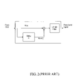
- FIG. 2 illustrates the configuration of a conventional demodulator
- FIG. 3 shows the analysis results of implementing the invention in a caller ID receiver unit
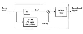
- FIG. 4 illustrates an exemplary configuration of a demodulator in which the invention is implemented
- FIG. 5 illustrates the performance result of implementing the invention in a caller ID receiver unit
- FIG. 6 illustrates a general purpose computing platform which may be used in implementing the invention.
- Standard demodulation techniques are known for demodulation of FSK signals.
- One of the standard techniques is the frequency discrimination method, which converts a change in frequency to a change in amplitude.
- Most of the discriminators find the autocorrelation between the signal and a time-shifted version of the signal to demodulate the FSK signal. Described herein is a method and apparatus with enhanced autocorrelation for better receiver performance, using the principles of the invention.
- FIG. 1 shows a FSK receiver with certain functional bocks.
- the signal from the analog front end is passed through a band pass filter (example, BPF 101 ) to remove out-of-band noise and near-end echo, incase of full-duplex modems.
- the AGC (automatic gain control) function is used to compensate for the channel attenuation and brings up the signal power to a reference level.
- the demodulator 103 then converts the signal to the original base band signal transmitted. This signal is then used by the baud clock recovery block 105 , which recovers the correct sample to slice.
- the slicer 104 is a comparator, which gives out bits 106 in the form of a symbol (0 or 1) after comparing the sample against a fixed threshold. Details of the functioning of the FSK receiver in FIG. 1 are intelligible to those who are skilled in the art.
- FIG. 2 A conventional demodulator illustrated in FIG. 1 is shown in FIG. 2 .
- the conventional demodulator shown in FIG. 2 has two parallel lines, the first having the received signal and the second line including a delay element to cause a delay of K.
- the signals from the two lines are multiplied and passed through a low pass base band filter to obtain the base band signal.
- the instantaneous frequency of the signal may be ( ⁇ c + ⁇ )/2 ⁇ or ( ⁇ c ⁇ )/2 ⁇ based on the binary digit sent.
- the product signal (3) is low pass filtered (equivalent to integration) the high frequency component will be removed and only the low frequency base band signal will be left.
- the DC value of the low pass filtered signal cos [( ⁇ c ⁇ )K] will depend on the time delay and the binary digit transmitted.
- the difference between the DC values corresponding to the binary digits should be maximized, with K being an integer not exceeding the number of samples in a baud. It is desirable that K should be as small as possible for the equations to hold good. Typically K should be less than half the number of samples in a baud.
- FIG. 3 illustrates the values of d( ⁇ ) and d(k) (which are represented on the Y axis) for different values of ⁇ /k (which are represented along the X axis).
- d( ⁇ ) is greater than d(k).
- ⁇ may be approximated to a K if the signal is highly over-sampled. But this is may not be feasible in terms of computation required.
- the signals being correlated may be delayed by a value close to ⁇ .
- FIG. 4 shows an exemplary modified demodulator structure, and shows a modified demodulator arrangement based on the discussion above.
- the demodulator is configured to include first and second parallel connected lines connected to the same input signal, the first line having a first signal with a delay M for the input signal coming into the demodulator, the second line generating a second signal after passing the input signal through a delay filter with a group delay of ⁇ +M where ⁇ is fractional.
- the delay filter is illustrated as an “All pass delay filter” As shown, the signals through the first and second parallel connected lines of the demodulator are multiplied and passed through a low pass base band filter to retrieve the base band signal.
- the signal coming into the demodulator is delayed in the second line by a value close to ⁇ +M, preferably using a delay filter which is designed as desired.
- the filter has a group delay response, which is close to ⁇ +M at least in the band of interest.
- M is the additional group delay that the filter might provide over and above the desired delay of ⁇ .
- the delay filter should have a unity gain at least in the band of interest.
- the filter may be designed using one of the polyphase components of a SINC interpolating filter, which gives a fractional delay close to the fractional delay in ( ⁇ +M). M in this case depends on the length of the SINC filter.
- the delay filter can be designed using any filter design tool that can design filters with an arbitrary amplitude and group delay response.
- R (n) in the first parallel line is the original signal delayed by an integer delay M. It is noted that R (n ⁇ ) in the second parallel line is the original signal delayed by ⁇ +M. The relative shift in time between these 2 signals is ⁇ .
- the signals in the first and second parallel lines, as explained earlier, are multiplied and low pass filtered to get the base band signal.
- a poly phase component of a SINC up-sampling filter of order 80 that up-samples by 4 can be chosen.
- the order of the filter may be reduced based on the accuracy of ⁇ required.
- the 4 th poly phase component of the filter described above has a group delay of 9.25 samples in the band of interest. This yields the value of M as 6.
- V.23/Bell 202A/CallerID receiver The performance of a V.23/Bell 202A/CallerID receiver as an example was evaluated with and without the inventive improvement and is shown in FIG. 5 .
- the above-described modification to a conventional FSK signal demodulator improves the performance of a FSK receiver.
- the demodulator is modified with filters to give a fractional sample shift, thereby increasing differences in the auto-correlation values of binary 0 and 1. This helps the slicer 104 (see FIG. 1 ) to make a better binary decision.
- the various operations within the FSK receiver may be coordinated and controlled by a general purpose computing platform as illustrated in FIG. 6 , or any other suitable arrangement.
- FIG. 6 Various embodiments of the present subject matter can be assisted by software, which may be run in the environment shown in FIG. 6 or in any other suitable computing environment.
- the embodiments of the present subject matter are operable in a number of general-purpose or special-purpose computing environments.
- Some computing environments include personal computers, general-purpose computers, server computers, hand-held devices (including, but not limited to, telephones and personal digital assistants (PDAs) of all types), laptop devices, multi-processors, microprocessors, set-top boxes, programmable consumer electronics, network computers, minicomputers, mainframe computers, distributed computing environments and the like to execute code stored on a computer-readable medium.
- PDAs personal digital assistants
- program modules include routines, programs, objects, components, data structures, and the like to perform particular tasks or to implement particular abstract data types.
- program modules may be located in local or remote storage devices.
- FIG. 6 and the following discussion are intended to provide a brief, general description of a suitable computing environment in which certain embodiments of the inventive concepts contained herein may be implemented.
- a general computing device 600 may include a computer 610 , a processing unit 602 , memory 604 , removable storage 612 , and non-removable storage 614 .
- Computer 610 additionally includes a bus 605 and a network interface (NI) 601 .
- NI network interface
- Computer 610 may include or have access to a computing environment that includes one or more user input modules or devices 616 , one or more output modules or devices 618 , and one or more communication connections 620 such as a network interface card or a USB connection.
- the one or more user input devices 616 can be a touch screen and a stylus and the like.
- the one or more output devices 618 can be a display device of computer, computer monitor, TV screen, plasma display, LCD display, display on a touch screen, display on an electronic tablet, and the like.
- the computer 610 may operate in a networked environment using the communication connection 620 to connect to one or more remote computers.
- a remote computer may include a personal computer, server, router, network PC, a peer device or other network node, and/or the like.
- the communication connection may include a Local Area Network (LAN), a Wide Area Network (WAN), and/or other networks.
- LAN Local Area Network
- WAN Wide Area Network
- the memory 604 may include volatile memory 606 and non-volatile memory 608 .
- volatile memory 606 and non-volatile memory 608 A variety of computer-readable media may be stored in and accessed from the memory elements of computer 610 , such as volatile memory 606 and non-volatile memory 608 , removable storage 601 and non-removable storage 614 .
- Computer memory elements can include any suitable memory device(s) for storing data and machine-readable instructions, such as read only memory (ROM), random access memory (RAM), erasable programmable read only memory (EPROM), electrically erasable programmable read only memory (EEPROM), hard drive, removable media drive for handling compact disks (CDs), digital video disks (DVDs), diskettes, magnetic tape cartridges, memory cards, Memory SticksTM, and the like, chemical storage, biological storage, and other types of data storage.
- ROM read only memory
- RAM random access memory
- EPROM erasable programmable read only memory
- EEPROM electrically erasable programmable read only memory
- hard drive removable media drive for handling compact disks (CDs), digital video disks (DVDs), diskettes, magnetic tape cartridges, memory cards, Memory SticksTM, and the like, chemical storage, biological storage, and other types of data storage.
- processor or “processing unit,” as used herein, means any type of computational circuit, such as, but not limited to, a microprocessor, a microcontroller, a complex instruction set computing (CISC) microprocessor, a reduced instruction set computing (RISC) microprocessor, a very long instruction word (VLIW) microprocessor, explicitly parallel instruction computing (EPIC) microprocessor, a graphics processor, a digital signal processor, or any other type of processor or processing circuit.
- CISC complex instruction set computing
- RISC reduced instruction set computing
- VLIW very long instruction word
- EPIC explicitly parallel instruction computing
- graphics processor a digital signal processor
- digital signal processor or any other type of processor or processing circuit.
- embedded controllers such as generic or programmable logic devices or arrays, application specific integrated circuits, single-chip computers, smart cards, and the like.
- Embodiments of the present subject matter may be implemented in conjunction with program modules, including functions, procedures, data structures, application programs, etc., for performing tasks, or defining abstract data types or low-level hardware contexts.
- Machine-readable instructions stored on any of the above-mentioned storage media are executable by the processing unit 602 of the computer 610 .
- a computer program 625 may include machine-readable instructions capable of handling a signal for an FSK receiver according to the teachings of the described embodiments of the present subject matter.
- the computer program 625 may be included on a CD-ROM and loaded from the CD-ROM to a hard drive in non-volatile memory 608 .
- the machine-readable instructions cause the computer 610 to decode according to the various embodiments of the present subject matter.
Landscapes
- Engineering & Computer Science (AREA)
- Computer Networks & Wireless Communication (AREA)
- Signal Processing (AREA)
- Digital Transmission Methods That Use Modulated Carrier Waves (AREA)
Abstract
Description
R(n)=cos [(ωc±δω)×n+φ] (1)
wherein, ωc is the 2*pi*carrier frequency, δω is the 2*pi*change in carrier frequency with binary digits, and φ is the initial phase of the signal. It is noted that the frequency and phase parameter are all in digital domain.
R(n−K)=cos [(ωc±δω)×(n−K)+φ] (2)
R(n)R(n−K)=cos [(ωc±δω)K]+cos [2(ωc±δω)n−(ωc±δω)K+2φ] (3)
- The product consists of 2 components, namely,
- 1. A dc component, cos [(ωc±δω)K] which changes with the binary data.
- 2. The other component cos [2(ωc±δω)n−(ωc±δω)K+2φ] is around twice the carrier frequency.
Binary 1: The DC value will be cos [(ωc−δω)K]= cos(2πf 1 K) (4)
Binary 0: The DC value will be cos [(ωc+δω)K]= cos(2πf 0 K) (5)
where f1 and f0 are mark and space frequencies represented in the digital domain. Let the absolute difference between the DC values be d(k).
d(k) may be expressed as d(K)=|cos(2πf 1 K)−cos(2πf 0 K)| (6)
d(τ)=|cos(2πf 1τ)−cos(2πf 0τ)| (7)
where τ is the continuous form of K. It is also noted that
d(τ)≧d(k) since τ can be varied continuously.
Claims (30)
Priority Applications (1)
| Application Number | Priority Date | Filing Date | Title |
|---|---|---|---|
| US11/224,776 US7474147B2 (en) | 2004-09-17 | 2005-09-13 | Frequency shift keying signal demodulator method and apparatus |
Applications Claiming Priority (2)
| Application Number | Priority Date | Filing Date | Title |
|---|---|---|---|
| US61125004P | 2004-09-17 | 2004-09-17 | |
| US11/224,776 US7474147B2 (en) | 2004-09-17 | 2005-09-13 | Frequency shift keying signal demodulator method and apparatus |
Publications (2)
| Publication Number | Publication Date |
|---|---|
| US20060062332A1 US20060062332A1 (en) | 2006-03-23 |
| US7474147B2 true US7474147B2 (en) | 2009-01-06 |
Family
ID=36073960
Family Applications (1)
| Application Number | Title | Priority Date | Filing Date |
|---|---|---|---|
| US11/224,776 Active 2027-05-21 US7474147B2 (en) | 2004-09-17 | 2005-09-13 | Frequency shift keying signal demodulator method and apparatus |
Country Status (1)
| Country | Link |
|---|---|
| US (1) | US7474147B2 (en) |
Families Citing this family (1)
| Publication number | Priority date | Publication date | Assignee | Title |
|---|---|---|---|---|
| US9906386B1 (en) * | 2017-01-13 | 2018-02-27 | Cypress Semiconductor Corporation | Frequency estimation, correction and noise suppression for modems |
Citations (7)
| Publication number | Priority date | Publication date | Assignee | Title |
|---|---|---|---|---|
| US4234930A (en) * | 1978-04-25 | 1980-11-18 | Her Majesty The Queen In Right Of Canada | Interleaved binary coded signal translation device |
| US5353301A (en) * | 1993-09-17 | 1994-10-04 | Motorola, Inc. | Method and apparatus for combining multipath spread-spectrum signals |
| US5627856A (en) * | 1994-09-09 | 1997-05-06 | Omnipoint Corporation | Method and apparatus for receiving and despreading a continuous phase-modulated spread spectrum signal using self-synchronizing correlators |
| US5774492A (en) * | 1996-08-02 | 1998-06-30 | General Electric Company | Low-complexity direct conversion receiver for delay-and-correlate transmitted reference signaling |
| US6151367A (en) * | 1997-06-30 | 2000-11-21 | Hyundai Electronics Ind. Co., Ltd. | Digital demodulator |
| US6900675B2 (en) * | 2003-09-02 | 2005-05-31 | Standard Microsystems Corporation | All digital PLL trimming circuit |
| US7397300B2 (en) * | 2003-09-09 | 2008-07-08 | Analog Devices, Inc. | FSK demodulator system and method |
-
2005
- 2005-09-13 US US11/224,776 patent/US7474147B2/en active Active
Patent Citations (7)
| Publication number | Priority date | Publication date | Assignee | Title |
|---|---|---|---|---|
| US4234930A (en) * | 1978-04-25 | 1980-11-18 | Her Majesty The Queen In Right Of Canada | Interleaved binary coded signal translation device |
| US5353301A (en) * | 1993-09-17 | 1994-10-04 | Motorola, Inc. | Method and apparatus for combining multipath spread-spectrum signals |
| US5627856A (en) * | 1994-09-09 | 1997-05-06 | Omnipoint Corporation | Method and apparatus for receiving and despreading a continuous phase-modulated spread spectrum signal using self-synchronizing correlators |
| US5774492A (en) * | 1996-08-02 | 1998-06-30 | General Electric Company | Low-complexity direct conversion receiver for delay-and-correlate transmitted reference signaling |
| US6151367A (en) * | 1997-06-30 | 2000-11-21 | Hyundai Electronics Ind. Co., Ltd. | Digital demodulator |
| US6900675B2 (en) * | 2003-09-02 | 2005-05-31 | Standard Microsystems Corporation | All digital PLL trimming circuit |
| US7397300B2 (en) * | 2003-09-09 | 2008-07-08 | Analog Devices, Inc. | FSK demodulator system and method |
Also Published As
| Publication number | Publication date |
|---|---|
| US20060062332A1 (en) | 2006-03-23 |
Similar Documents
| Publication | Publication Date | Title |
|---|---|---|
| US9270390B2 (en) | Frequency and phase offset compensation of modulated signals with symbol timing recovery | |
| EP0036084B1 (en) | Process and device for the control of the initial adjustment of the clock of a receiver for synchronous data | |
| US10454729B2 (en) | Synchronization for low-energy long-range communications | |
| EP3621259B1 (en) | Method and device for fsk/gfsk demodulation | |
| WO1998023070A9 (en) | Passband dqpsk detector for a digital communications receiver | |
| US4518922A (en) | Decision-directed, automatic frequency control technique for non-coherently demodulated M-ARY frequency shift keying | |
| US9912512B2 (en) | Systems and methods for frequency synchronization between transmitters and receivers in a communication system | |
| EP1847040B1 (en) | Method and system for synchronization between a transmitter and a receiver in a wireless communication system | |
| US5758277A (en) | Transient analysis system for characterizing RF transmitters by analyzing transmitted RF signals | |
| KR101067265B1 (en) | Timing synchronization for M-DPSK channels | |
| JP2008530951A (en) | Demodulator and receiver for pre-encoded partial response signals | |
| US6959054B2 (en) | Filter bank and receiver for processing continuous phase modulated signals | |
| US7474147B2 (en) | Frequency shift keying signal demodulator method and apparatus | |
| US20070025466A1 (en) | System and method for transmission and reception of qam signals at low signal to noise ratio | |
| US6879647B1 (en) | Radio receiver AM-MSK processing techniques | |
| EP0614582A1 (en) | Digital demodulator for preamble-less burst communications | |
| US8208572B2 (en) | Method for transmitting and receiving quadrature amplitude modulation signals, a system for carrying out said method, a machine-readable carrier and the use of a method for synchronously receiving quadrature amplitude modulation signals | |
| EP0903884A2 (en) | Phase estimating circuit and demodulating circuit | |
| Tibenderana et al. | Low-complexity high-performance GFSK receiver with carrier frequency offset correction | |
| JP4747064B2 (en) | Preamble detection device and radio receiver | |
| US6785347B1 (en) | Nonlinear-least squares based method and apparatus for FSK signal decoding | |
| JP5202285B2 (en) | Symbol clock detection circuit, analog / digital identification circuit, and modulation system identification device | |
| Gunther et al. | Burst mode synchronization of QPSK on AWGN channels using kurtosis | |
| Chan et al. | Estimation of symbol rate from the autocorrelation function | |
| JPH01101049A (en) | Receiver |
Legal Events
| Date | Code | Title | Description |
|---|---|---|---|
| AS | Assignment |
Owner name: ITTIAM SYSTEMS (P) LTD., INDIANA Free format text: ASSIGNMENT OF ASSIGNORS INTEREST;ASSIGNOR:PATRA, GOPINATH;REEL/FRAME:016982/0183 Effective date: 20050909 |
|
| STCF | Information on status: patent grant |
Free format text: PATENTED CASE |
|
| FPAY | Fee payment |
Year of fee payment: 4 |
|
| AS | Assignment |
Owner name: BROADCOM CORPORATION, CALIFORNIA Free format text: ASSIGNMENT OF ASSIGNORS INTEREST;ASSIGNOR:ITTIAM SYSTEMS PRIVATE LIMITED;REEL/FRAME:033423/0615 Effective date: 20140530 Owner name: BROADCOM INTERNATIONAL LIMITED, CAYMAN ISLANDS Free format text: ASSIGNMENT OF ASSIGNORS INTEREST;ASSIGNOR:ITTIAM SYSTEMS PRIVATE LIMITED;REEL/FRAME:033423/0615 Effective date: 20140530 |
|
| FEPP | Fee payment procedure |
Free format text: PAT HOLDER NO LONGER CLAIMS SMALL ENTITY STATUS, ENTITY STATUS SET TO UNDISCOUNTED (ORIGINAL EVENT CODE: STOL); ENTITY STATUS OF PATENT OWNER: LARGE ENTITY |
|
| AS | Assignment |
Owner name: BANK OF AMERICA, N.A., AS COLLATERAL AGENT, NORTH CAROLINA Free format text: PATENT SECURITY AGREEMENT;ASSIGNOR:BROADCOM CORPORATION;REEL/FRAME:037806/0001 Effective date: 20160201 Owner name: BANK OF AMERICA, N.A., AS COLLATERAL AGENT, NORTH Free format text: PATENT SECURITY AGREEMENT;ASSIGNOR:BROADCOM CORPORATION;REEL/FRAME:037806/0001 Effective date: 20160201 |
|
| FPAY | Fee payment |
Year of fee payment: 8 |
|
| AS | Assignment |
Owner name: AVAGO TECHNOLOGIES GENERAL IP (SINGAPORE) PTE. LTD., SINGAPORE Free format text: ASSIGNMENT OF ASSIGNORS INTEREST;ASSIGNOR:BROADCOM CORPORATION;REEL/FRAME:041706/0001 Effective date: 20170120 Owner name: AVAGO TECHNOLOGIES GENERAL IP (SINGAPORE) PTE. LTD Free format text: ASSIGNMENT OF ASSIGNORS INTEREST;ASSIGNOR:BROADCOM CORPORATION;REEL/FRAME:041706/0001 Effective date: 20170120 |
|
| AS | Assignment |
Owner name: BROADCOM CORPORATION, CALIFORNIA Free format text: TERMINATION AND RELEASE OF SECURITY INTEREST IN PATENTS;ASSIGNOR:BANK OF AMERICA, N.A., AS COLLATERAL AGENT;REEL/FRAME:041712/0001 Effective date: 20170119 |
|
| AS | Assignment |
Owner name: AVAGO TECHNOLOGIES INTERNATIONAL SALES PTE. LIMITE Free format text: MERGER;ASSIGNOR:AVAGO TECHNOLOGIES GENERAL IP (SINGAPORE) PTE. LTD.;REEL/FRAME:047195/0658 Effective date: 20180509 |
|
| AS | Assignment |
Owner name: AVAGO TECHNOLOGIES INTERNATIONAL SALES PTE. LIMITE Free format text: CORRECTIVE ASSIGNMENT TO CORRECT THE EFFECTIVE DATE OF MERGER PREVIOUSLY RECORDED ON REEL 047195 FRAME 0658. ASSIGNOR(S) HEREBY CONFIRMS THE THE EFFECTIVE DATE IS 09/05/2018;ASSIGNOR:AVAGO TECHNOLOGIES GENERAL IP (SINGAPORE) PTE. LTD.;REEL/FRAME:047357/0302 Effective date: 20180905 |
|
| AS | Assignment |
Owner name: AVAGO TECHNOLOGIES INTERNATIONAL SALES PTE. LIMITE Free format text: CORRECTIVE ASSIGNMENT TO CORRECT THE ERROR IN RECORDING THE MERGER PREVIOUSLY RECORDED AT REEL: 047357 FRAME: 0302. ASSIGNOR(S) HEREBY CONFIRMS THE ASSIGNMENT;ASSIGNOR:AVAGO TECHNOLOGIES GENERAL IP (SINGAPORE) PTE. LTD.;REEL/FRAME:048674/0834 Effective date: 20180905 |
|
| MAFP | Maintenance fee payment |
Free format text: PAYMENT OF MAINTENANCE FEE, 12TH YEAR, LARGE ENTITY (ORIGINAL EVENT CODE: M1553); ENTITY STATUS OF PATENT OWNER: LARGE ENTITY Year of fee payment: 12 |