US7485508B2 - Two-sided semiconductor-on-insulator structures and methods of manufacturing the same - Google Patents
Two-sided semiconductor-on-insulator structures and methods of manufacturing the same Download PDFInfo
- Publication number
- US7485508B2 US7485508B2 US11/627,653 US62765307A US7485508B2 US 7485508 B2 US7485508 B2 US 7485508B2 US 62765307 A US62765307 A US 62765307A US 7485508 B2 US7485508 B2 US 7485508B2
- Authority
- US
- United States
- Prior art keywords
- type mosfet
- semiconductor layer
- forming
- stress
- layer
- Prior art date
- Legal status (The legal status is an assumption and is not a legal conclusion. Google has not performed a legal analysis and makes no representation as to the accuracy of the status listed.)
- Active, expires
Links
Images


Classifications
-
- H—ELECTRICITY
- H01—ELECTRIC ELEMENTS
- H01L—SEMICONDUCTOR DEVICES NOT COVERED BY CLASS H10
- H01L27/00—Devices consisting of a plurality of semiconductor or other solid-state components formed in or on a common substrate
- H01L27/02—Devices consisting of a plurality of semiconductor or other solid-state components formed in or on a common substrate including semiconductor components specially adapted for rectifying, oscillating, amplifying or switching and having at least one potential-jump barrier or surface barrier; including integrated passive circuit elements with at least one potential-jump barrier or surface barrier
- H01L27/04—Devices consisting of a plurality of semiconductor or other solid-state components formed in or on a common substrate including semiconductor components specially adapted for rectifying, oscillating, amplifying or switching and having at least one potential-jump barrier or surface barrier; including integrated passive circuit elements with at least one potential-jump barrier or surface barrier the substrate being a semiconductor body
- H01L27/06—Devices consisting of a plurality of semiconductor or other solid-state components formed in or on a common substrate including semiconductor components specially adapted for rectifying, oscillating, amplifying or switching and having at least one potential-jump barrier or surface barrier; including integrated passive circuit elements with at least one potential-jump barrier or surface barrier the substrate being a semiconductor body including a plurality of individual components in a non-repetitive configuration
- H01L27/0688—Integrated circuits having a three-dimensional layout
- H01L27/0694—Integrated circuits having a three-dimensional layout comprising components formed on opposite sides of a semiconductor substrate
-
- H—ELECTRICITY
- H01—ELECTRIC ELEMENTS
- H01L—SEMICONDUCTOR DEVICES NOT COVERED BY CLASS H10
- H01L21/00—Processes or apparatus adapted for the manufacture or treatment of semiconductor or solid state devices or of parts thereof
- H01L21/70—Manufacture or treatment of devices consisting of a plurality of solid state components formed in or on a common substrate or of parts thereof; Manufacture of integrated circuit devices or of parts thereof
- H01L21/77—Manufacture or treatment of devices consisting of a plurality of solid state components or integrated circuits formed in, or on, a common substrate
- H01L21/78—Manufacture or treatment of devices consisting of a plurality of solid state components or integrated circuits formed in, or on, a common substrate with subsequent division of the substrate into plural individual devices
- H01L21/82—Manufacture or treatment of devices consisting of a plurality of solid state components or integrated circuits formed in, or on, a common substrate with subsequent division of the substrate into plural individual devices to produce devices, e.g. integrated circuits, each consisting of a plurality of components
- H01L21/84—Manufacture or treatment of devices consisting of a plurality of solid state components or integrated circuits formed in, or on, a common substrate with subsequent division of the substrate into plural individual devices to produce devices, e.g. integrated circuits, each consisting of a plurality of components the substrate being other than a semiconductor body, e.g. being an insulating body
-
- H—ELECTRICITY
- H01—ELECTRIC ELEMENTS
- H01L—SEMICONDUCTOR DEVICES NOT COVERED BY CLASS H10
- H01L23/00—Details of semiconductor or other solid state devices
- H01L23/48—Arrangements for conducting electric current to or from the solid state body in operation, e.g. leads, terminal arrangements ; Selection of materials therefor
- H01L23/481—Internal lead connections, e.g. via connections, feedthrough structures
-
- H—ELECTRICITY
- H01—ELECTRIC ELEMENTS
- H01L—SEMICONDUCTOR DEVICES NOT COVERED BY CLASS H10
- H01L23/00—Details of semiconductor or other solid state devices
- H01L23/48—Arrangements for conducting electric current to or from the solid state body in operation, e.g. leads, terminal arrangements ; Selection of materials therefor
- H01L23/482—Arrangements for conducting electric current to or from the solid state body in operation, e.g. leads, terminal arrangements ; Selection of materials therefor consisting of lead-in layers inseparably applied to the semiconductor body
- H01L23/485—Arrangements for conducting electric current to or from the solid state body in operation, e.g. leads, terminal arrangements ; Selection of materials therefor consisting of lead-in layers inseparably applied to the semiconductor body consisting of layered constructions comprising conductive layers and insulating layers, e.g. planar contacts
-
- H—ELECTRICITY
- H01—ELECTRIC ELEMENTS
- H01L—SEMICONDUCTOR DEVICES NOT COVERED BY CLASS H10
- H01L27/00—Devices consisting of a plurality of semiconductor or other solid-state components formed in or on a common substrate
- H01L27/02—Devices consisting of a plurality of semiconductor or other solid-state components formed in or on a common substrate including semiconductor components specially adapted for rectifying, oscillating, amplifying or switching and having at least one potential-jump barrier or surface barrier; including integrated passive circuit elements with at least one potential-jump barrier or surface barrier
- H01L27/12—Devices consisting of a plurality of semiconductor or other solid-state components formed in or on a common substrate including semiconductor components specially adapted for rectifying, oscillating, amplifying or switching and having at least one potential-jump barrier or surface barrier; including integrated passive circuit elements with at least one potential-jump barrier or surface barrier the substrate being other than a semiconductor body, e.g. an insulating body
- H01L27/1203—Devices consisting of a plurality of semiconductor or other solid-state components formed in or on a common substrate including semiconductor components specially adapted for rectifying, oscillating, amplifying or switching and having at least one potential-jump barrier or surface barrier; including integrated passive circuit elements with at least one potential-jump barrier or surface barrier the substrate being other than a semiconductor body, e.g. an insulating body the substrate comprising an insulating body on a semiconductor body, e.g. SOI
Definitions
- the present invention relates to semiconductor devices, and particularly to semiconductor structures having semiconductor devices on both sides of a semiconductor-on-insulator substrate and methods of fabricating the same.
- CMOS integrated circuits comprise p-type devices and n-type devices formed on the same level in a semiconductor substrate, i.e., the various components of p-type devices are coplanar with the corresponding components of the n-type devices.
- Some of the processing steps are common to both the p-type devices and the n-type devices, but many steps are not common and thus need to be performed separately by masking the area for one type of device while processing the other type of device.
- the p-type and n-type devices require different well implantation, different gate polysilicon implantation, and different source and drain implantation.
- the processing conditions are in general not optimal for either the p-type devices or for the n-type devices, but instead a compromise between the two different optimal conditions is made.
- the stress of shallow trench isolation cannot be simultaneously optimized for both p-type devices and n-type devices since an optimal stress for a p-type metal-oxide-semiconductor field effect transistor (MOSFET) is compressive, while an optimal stress for an n-type MOSFET is tensile.
- MOSFET metal-oxide-semiconductor field effect transistor
- the structure of a gate stack is another example in which different processes between the p-type and n-type devices can improve the performance of both types of MOSFETs.
- boundary area A consequence of forming both types of semiconductor devices on the same level is the formation of a boundary area between the two types of devices. Due to a finite overlay tolerance of the block masks, the boundary area needs to be at least as wide as the overlay tolerance of the block masks. Since p-type devices and n-type devices need to be placed in proximity, the boundary area may occupy a substantial portion of the total semiconductor area in high performance CMOS circuits. Furthermore, requirements for inter-well isolation also increase the boundary area between the two types of semiconductor devices.
- one group of high performance CMOS devices requires using a particular type of material and processing steps, while another group of high performance CMOS devices require using a different type of material and processing steps.
- the two groups of high performance CMOS devices need to be physically placed in close proximity to facilitate wiring and to reduce delay in signal propagation.
- Use of block masks not only increases the process complexity and cost, but also reduces the packing density due to the requirement for boundary areas between the two groups of devices.
- the present invention addresses the needs described above by providing a semiconductor structure with at least one first type semiconductor device located above a buried insulator layer of a semiconductor-on-insulator (SOI) substrate and with at least one second type semiconductor device located beneath the buried insulator layer of the SOI substrate.
- SOI semiconductor-on-insulator
- the present invention addresses the needs described above by providing a method of manufacturing a semiconductor structure by forming the at least one first type semiconductor device above a buried insulator layer of a semiconductor-on-insulator (SOI) substrate and by forming the at least one second type semiconductor device beneath the buried insulator layer of the SOI substrate.
- SOI semiconductor-on-insulator
- a semiconductor structure comprises:
- At least one second type MOSFET located on a second semiconductor layer, wherein the second semiconductor layer directly contacts a top surface of the buried insulator layer.
- the semiconductor structure according to the present invention may further comprise:
- MOL middle-of-line
- the materials and process parameters for the at least one first type MOSFET and the at least one second type MOSFET may be independently optimized.
- Such materials and process parameters include surface orientations of the first and second semiconductor layers, the material for shallow trench isolation (STI) and consequent stresses applied to devices by the STI, stress liners on the first type and second type MOSFETs, semiconductor material for the first and second semiconductor layers, embedded material within source and drain regions of the MOSFETs and consequent stresses applied to the channel of the two types of MOSFETs, gate electrode materials for the gate dielectric layers and/or the gate conductors.
- the semiconductor structure according to the present invention may further comprise an alignment structure that allows alignment of the semiconductor structure both with the top semiconductor layer on the upside of the buried insulator layer and with the bottom semiconductor layer on the upside of the buried insulator layer.
- the semiconductor structure according to the present invention may further comprise:
- MOL middle-of-line
- At least one conductive via through the second MOL dielectric layer, through the second semiconductor layer, and through the buried insulator layer.
- the semiconductor structure further comprises at least one metal wiring that contacts the at least one conductive via and the second MOL dielectric layer.
- a method of manufacturing the semiconductor structure described above comprises:
- SOI semiconductor-on-insulator
- first middle-of-line (MOL) dielectric layer on the at least one first type MOSFET
- the method of manufacturing the semiconductor structure described above may further comprise:
- MOL middle-of-line
- the method of manufacturing the semiconductor structure further comprises forming at least one metal wiring that contacts the at least one conductive via and the second MOL dielectric layer.
- the method of manufacturing the semiconductor structure further comprises:
- the first type semiconductor devices and the second type semiconductor devices are formed separately. Therefore, different materials and different process parameters may be utilized to optimize the performance of the first type MOSFETs and the second type MOSFETs independently.
- the optimization of the device performance is not necessarily limited to MOSFET devices, but may be extended to any other semiconductor devices including passive devices such as resistors, capacitors, diodes, and varactors.
- Any process parameters and materials may therefore be utilized to optimize the semiconductor devices on the first semiconductor layer and the semiconductor devices on the second semiconductor layer independently including the materials and process parameters listed above.
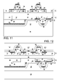
- FIGS. 1 , 2 , 2 A, 2 B, 3 - 8 , 8 A, 8 B, and 9 - 13 are sequential vertical cross-sectional views illustrating the basic processing steps for manufacturing an exemplary semiconductor structure according to the present invention.
- the present invention relates to a semiconductor structure and methods of manufacturing the same, in which first type semiconductor devices are formed on one side of a buried insulator layer and second type semiconductor devices are formed on the other side of the buried insulator layer, which is now described in detail with accompanying figures.
- a semiconductor-on-insulator (SOI) substrate is provided.
- the SOI substrate comprises a carrier substrate 10 , a buried insulator layer 20 , and a first semiconductor layer 30 . Since the SOI substrate is later flipped upside down, the first semiconductor layer 30 is physically located beneath the buried insulator layer 20 in the final structure. For this reason, the first interface 25 between the buried insulator layer 20 and the first semiconductor layer 30 is herein referred to as a “bottom surface” of the buried insulator layer 20 . For a similar reason, the second interface 15 between the buried insulator layer 20 and the carrier substrate 10 is herein referred to as a “top surface” of the buried insulator layer 20 .
- the first semiconductor layer 30 has an exposed first surface 35 with a first surface orientation, which is the crystallographic orientation of the first semiconductor layer 30 in the direction of the surface normal of the first surface 35 .
- the carrier substrate 10 has an exposed second surface 5 with a second surface orientation, which is the crystallographic orientation of the carrier substrate 10 in the direction of the surface normal of the second surface 5 .
- the surface orientations of the first semiconductor layer 30 and of the carrier substrate 10 respectively, refer to the first surface orientation and to the second surface orientation.
- the semiconductor material of the first semiconductor layer 30 is optimized for performance of at least one first type MOSFET to be subsequently formed thereupon.
- the semiconductor material in the carrier substrate 10 is optimized for performance of at least one second type MOSFET. Therefore, the semiconductor material in the first semiconductor layer 30 and the semiconductor material in the carrier substrate 10 may be the same or may be different.
- the crystallographic orientations, and especially the surface orientations, which is the crystallographic orientations of the surface normal of a semiconductor layer may be the same or different between the first semiconductor layer 30 and the carrier substrate 10 .
- Non-limiting examples of semiconductor material comprising each of the first semiconductor layer 30 and the carrier substrate 10 may be one of the following: silicon, germanium, silicon-germanium alloy, silicon carbon alloy, silicon-germanium-carbon alloy, gallium arsenide, indium arsenide, indium phosphide, III-V compound semiconductor materials, II-VI compound semiconductor materials, organic semiconductor materials, and other compound semiconductor materials.
- Non-limiting examples of surface orientations for the first semiconductor layer 30 and for the carrier substrate 10 include (100), (110), (111), (211), (221), (311), (321), and (331). Any combination of semiconductor material and surface orientation may be employed to optimize device performance for each of the at least one first type MOSFET and the at least one second type MOSFET.
- first shallow trench isolation (STI) 34 is formed within the first semiconductor layer 30 by conventional methods such as deposition of pad layers, lithographic patterning of the pad layers, deposition of a first STI material, and planarization. The remaining portions of the first semiconductor layer 30 that are not occupied by the first STI 34 form first active areas 32 .
- the first STI material may be selected to apply optimal stress to the first active areas 32 for the at least one first type MOSFET to be formed thereupon. For example, if the at least one first type MOSFET to be formed in the first semiconductor layer 30 is a p-type MOSFET, the first STI may apply a compressive stress to the first active areas 32 .
- the first STI may apply a tensile stress to the first active areas 32 .
- Suitable STI liners may be employed as needed.
- Some of the first STI 34 may be used to form alignment marks that may be used to align a semiconductor structure on the first semiconductor layer 30 and subsequently to align a semiconductor structure to be formed on a remaining portion of the carrier substrate 10 after removing a portion of the carrier substrate 10 and flipping the semiconductor structure upside down.
- a first alternative semiconductor structure with a first alternative alignment mark 36 is shown which is formed by etching the first semiconductor layer 30 , the buried insulator layer 20 , and a portion of the carrier substrate 10 .
- the depth of the first alternative alignment mark 36 is selected such that the first alternative alignment mark 36 does not extend to the surface of a remaining portion of the carrier substrate 10 after removing a portion of the carrier substrate as will be shown below.
- a second alternative semiconductor structure with a second alternative alignment mark 38 is shown which is formed by etching the first semiconductor layer 30 , the buried insulator layer 20 , and a portion of the carrier substrate 10 .
- the depth of the second alternative alignment mark 38 is selected such that the second alternative alignment mark 38 extends to the surface of a remaining portion of the carrier substrate 10 after removing a portion of the carrier substrate as will be shown below.
- At least one first type MOSFET is partially formed by depositing a first gate stack, lithographically patterning the first gate stack, and forming suitable first spacers 48 as well as implantation of suitable dopants.
- block masks are not needed to differentiate one type of devices from another since the present invention allows the formation of one type of devices on one side of the buried insulator layer 20 .
- Devices of the other type are subsequently formed on the other side of the buried insulator layer 20 .
- a first gate stack that comprises a first gate dielectric layer 42 , a first gate conductor layer 44 , and a first gate cap layer 46 are formed on the first semiconductor layer 30 .
- the first gate stack ( 42 , 44 , 46 ) is subsequently lithographically patterned and etched to form first gate electrodes.
- First source and drain extension regions 47 may be formed by suitable implantation.
- the first spacers 48 are formed as needed by deposition of a first dielectric layer followed by a reactive ion etch (RIE).
- RIE reactive ion etch
- the first gate dielectric layer 42 , the first gate conductor layer 44 , and the first gate cap layer 46 are optimized for the performance of the at least one first type MOSFET with disregard to considerations for performance of the at least one second type MOSFET to be formed subsequently.
- materials and process parameters for the components of the first gate stack ( 42 , 44 , 46 ) may be optimized only for the performance of the at least one first type MOSFET.
- a high-K dielectric material and a metal gate material suitable for the at least one first type MOSFET may be utilized for the first gate stack ( 42 , 44 , 46 ).
- the polysilicon may be in-situ doped at an optimal level for the at least one first type MOSFET.
- first source and drain regions 52 are formed by ion implantation.
- a first embedded material may be formed within the first source and drain regions 52 either by implantation of additional material followed by an anneal or by etching of at least a portion of the first source and drain region 52 followed by deposition of the first embedded material.
- Implantation into the first gate conductor layer 44 may be performed as needed.
- the first gate cap layer 46 is removed prior to a first silicidation. After appropriate surface preparations such as a wet etch, a first metal (not shown) is deposited and reacted with underlying semiconductor materials to form a first source and drain silicide 54 and a first gate silicide 56 .
- Process parameters for the first metal such as composition, deposited thickness, and deposition method as well as process parameters for the metallization such as anneal temperatures and duration of the anneal process, which are well known in the prior art, are optimized for the performance of the at least one first type MOSFET with disregard to considerations for performance of at least one second type MOSFET to be formed subsequently.
- materials and process parameters for the components of the first source and drain silicide 54 and the first gate silicide 56 may be optimized only for the performance of the at least one first type MOSFET.
- a first stress liner 60 may be formed directly on the at least one first type MOSFET.
- a first stress liner 60 is a dielectric layer that applies a stress to the channel of the at least one first type MOSFET such that the minority carrier mobility is enhanced in the channel of the at least one first type MOSFET.
- the at least one first type MOSFET comprises a p-type MOSFET
- the first stress liner 60 preferably applies a compressive stress to the channel of the at least one first type MOSFET.
- the at least one first type MOSFET comprises an n-type MOSFET
- the first stress liner 60 preferably applies a tensile stress to the channel of the at least one first type MOSFET.
- a first middle-of-the-line (MOL) dielectric layer 62 is deposited and planarized.
- the first MOL dielectric layer 62 may be a doped or undoped oxide.
- the first MOL dielectric layer 62 may or may not apply stress to the channel of the at least one first type MOSFET.
- the material and process parameters for the first MOL dielectric layer 62 which are well known in the prior art, are optimized for the performance of the at least one first type MOSFET.
- a hydrogen implant may be performed into the carrier substrate 10 to facilitate a subsequent cleaving of the carrier substrate 10 .
- the depth of the hydrogen implant 11 as measured from the second interface 15 between the carrier substrate 10 and the buried insulator layer 20 determines the thickness t of the remaining semiconductor layer (to be referred to as a “second semiconductor layer” subsequently) after cleaving.
- Alternative methods for removing a portion of the carrier substrate 11 without employing a hydrogen implantation may also be utilized, in which case a hydrogen implantation at this stage is not necessary.
- a handle wafer 64 is bonded to the planarized first MOL layer 62 .
- the handle wafer 64 may comprise a semiconductor material, a conducting material, or an insulating material.
- the handle wafer 64 may be bonded at a low temperature, e.g., below 500° C. to avoid cleaving of the carrier substrate 10 if a hydrogen implant is used prior to bonding.
- a lower portion 10 ′ of the carrier substrate 10 is removed preferably by cleaving the lower portion 10 ′ from the rest of the semiconductor structure. If a hydrogen implant is used prior to bonding of the handle wafer 64 with the planarized first MOL dielectric layer 62 and a low temperature bonding, i.e., at a temperature below 500° C., is utilized during the bonding, the cleaving is performed by subjecting the semiconductor structure to a temperature above 500° C. to facilitate cleaving.
- the bonding of the handle wafer 64 with the planarized first MOL dielectric 62 and the cleaving of the carrier substrate 10 into a lower portion 10 ′ and the second semiconductor layer 70 may be performed at the same time at a temperature above 500° C.
- the lower portion 10 ′ of the carrier substrate 10 may be removed by other methods such as chemical mechanical planarization.
- the second semiconductor layer 70 is the remaining portion of the carrier substrate 10 after cleaving.
- the interface between the second semiconductor layer 70 and the buried insulator layer 20 is the same interface between the original carrier substrate 10 and the buried insulator layer 20 , which is the second interface 15 , or the “top surface” of the buried insulator layer 20 as shown in FIG. 7 .
- the remaining semiconductor structure that comprises the buried insulator layer 20 is flipped upside down.
- the second interface 15 , or the “top surface” of the buried insulator layer 20 is now located at the “top” of the buried insulator layer 20 .
- the first interface 25 , or the “bottom surface” of the buried insulator layer 20 is now located at the “bottom” of the buried insulator layer 20 .
- the surface orientation of the second semiconductor layer 70 is the orientation of the surface normal of the second semiconductor layer surface 75 and is the same as the second surface orientation, which is the surface orientation of the carrier substrate 10 prior to cleaving.
- Alignment marks formed in the first STI 34 may be used to align the semiconductor structure after flipping the semiconductor structure upside down. Preferably, multiple alignment marks are utilized for precise alignment of structures in the second semiconductor layer 70 in subsequent processing steps.
- the first alternative semiconductor structure with a first alternative alignment mark 36 is shown at the stage of semiconductor processing corresponding to FIG. 8 .
- the first alternative alignment mark 36 does not extend to the second semiconductor layer surface 75 .
- multiple first alternative alignment marks 36 are utilized for precise alignment of structures in the second semiconductor layer 70 in subsequent processing steps.
- the second alternative semiconductor structure with a second alternative alignment mark 38 is shown at the stage of semiconductor processing corresponding to FIG. 8 .
- the second alternative alignment mark 38 extends to the second semiconductor layer surface 75 .
- multiple second alternative alignment marks 38 are utilized for precise alignment of structures in the second semiconductor layer 70 in subsequent processing steps.
- second shallow trench isolation (STI) 74 is formed within the second semiconductor layer 70 by conventional methods such as deposition of pad layers, lithographic patterning of the pad layers, deposition of a second STI material, and planarization. The remaining portions of the second semiconductor layer 70 that are not occupied by the second STI 74 form second active areas 72 .
- the second STI material may be selected to apply optimal stress to the second active areas 72 for the at least one second type MOSFET to be formed thereupon. For example, if the at least one second type MOSFET to be formed in the second semiconductor layer 70 is an n-type MOSFET, the second STI may apply a tensile stress to the second active areas 72 .
- the second STI may apply a compressive stress to the second active areas 32 .
- Suitable STI liners may be employed as needed.
- the first STI material and the second STI material may be the same or different.
- At least one second type MOSFET is partially formed by depositing a second gate stack, lithographically patterning the second gate stack, and forming suitable second spacers 88 as well as implantation of suitable dopants.
- block masks are not needed to differentiate one type of devices from another since the present invention allows the formation of one type of devices on one side of the buried insulator layer 20 , that is on the first semiconductor layer 30 , while forming the other type of devices on the other side of the buried insulator layer 20 , that is, on the second semiconductor layer 70 .
- a second gate stack that comprises a second gate dielectric layer 82 , a second gate conductor layer 84 , and a second gate cap layer 86 are formed on the second semiconductor layer 70 .
- the second gate stack ( 82 , 84 , 86 ) is subsequently lithographically patterned and etched to form second gate electrodes.
- the composition of the first gate stack ( 42 , 44 , 46 ) may be the same as or may be different from the composition of the second gate stack ( 82 , 84 , 86 ).
- the composition of the first gate stack ( 42 , 44 , 46 ) is different from the composition of the second gate stack ( 82 , 84 , 86 ) to optimize the performance of the at least one first type MOSFET and the at least one second type MOSFET independently.
- Second source and drain extension regions 87 may be formed by suitable implantation.
- the second spacers 88 are formed as needed by deposition of a second dielectric layer followed by a reactive ion etch (RIE).
- RIE reactive ion etch
- the material for the first spacers 48 and the material for the second spacers 88 may be the same or different.
- the second gate dielectric layer 82 , the second gate conductor layer 84 , and the second gate cap layer 86 are optimized for the performance of the at least one second type MOSFET with disregard to considerations for performance of at least one first type MOSFET that has been formed before except for the impact of thermal cycling on the thermal diffusion of dopants in the at least one first type MOSFET.
- materials and process parameters for the components of the second gate stack ( 82 , 84 , 86 ) may be optimized only for the performance of the at least one second type MOSFET.
- a high-K dielectric material and a metal gate material suitable for the at least one second type MOSFET may be utilized for the second gate stack ( 82 , 84 , 86 ).
- the polysilicon may be in-situ doped at an optimal level for the at least one second type MOSFET.
- second source and drain regions 92 are formed by ion implantation.
- a second embedded material may be formed within the second source and drain regions 92 either by implantation of additional material followed by an anneal or by etching of at least a portion of the second source and drain region 92 followed by deposition of a second embedded material.
- Implantation into the second gate conductor layer 84 may be performed as needed.
- the second gate cap layer 86 is removed prior to a second silicidation. After appropriate surface preparations such as a wet etch, a second metal (not shown) is deposited and reacted with underlying semiconductor materials to form a second source and drain silicide 94 and a second gate silicide 96 .
- Process parameters for the second metal such as composition, deposited thickness, and deposition method as well as process parameters for the metallization such as anneal temperatures and duration of the anneal process are optimized for the performance of the at least one second type MOSFET with disregard to considerations for performance of at least one second type MOSFET that has been formed before except for the impact of thermal cycling on the thermal diffusion of dopants in the at least one first type MOSFET.
- materials and process parameters for the components of the second source and drain silicide 94 and the second gate silicide 96 may be optimized only for the performance of the at least one second type MOSFET.
- a second stress liner 100 may be formed directly on the at least one second type MOSFET.
- a second stress liner 100 is a dielectric layer that applies a stress to the channel of the at least one second type MOSFET such that the minority carrier mobility is enhanced in the channel of the at least one second type MOSFET.
- the at least one second type MOSFET comprises an n-type MOSFET
- the second stress liner 100 preferably applies a tensile stress to the channel of the at least one second type MOSFET.
- the at least one second type MOSFET comprises a p-type MOSFET
- the second stress liner 100 preferably applies a compressive stress to the channel of the at least one second type MOSFET.
- a second middle-of-the-line (MOL) dielectric layer 102 is deposited and planarized.
- the second MOL dielectric layer 102 may be a doped or undoped oxide.
- the second MOL dielectric layer may or may not apply stress to the channel of the at least one second type MOSFET.
- the material and process parameters for the second MOL dielectric layer 102 are optimized for the performance of the at least one second type MOSFET.
- via holes are formed through at least the second MOL dielectric layer 102 and filled with a conductive material to form conductive vias 112 .
- at least one conductive via 112 is formed through the buried insulator layer 20 to connect both sides of the buried insulator layer 20 electrically.
- the top of the conductive vias is coincident with the top surface of the second MOL dielectric layer 102 .
- the bottom of the conductive vias may be located within or on a second gate silicide 96 , within or on a second source and drain silicide 94 , within or on a first source and drain silicide 54 , or within or on a first gate silicide 56 .
- a conductive via 112 that connects a first type MOSFET and a second type MOSFET spans the second MOL dielectric layer 102 , the second semiconductor layer 70 , the buried insulator layer 20 , and the first semiconductor layer 30 and may or may not span the first MOL dielectric layer 62 .
- at least one metal wiring 120 is formed on top of the conductive vias 112 such that the at least one metal wiring contacts the conductive vias 112 and the second MOL dielectric layer 102 .
Abstract
Description
Claims (20)
Priority Applications (3)
| Application Number | Priority Date | Filing Date | Title |
|---|---|---|---|
| US11/627,653 US7485508B2 (en) | 2007-01-26 | 2007-01-26 | Two-sided semiconductor-on-insulator structures and methods of manufacturing the same |
| TW097102500A TWI411059B (en) | 2007-01-26 | 2008-01-23 | Two-sided semiconductor-on-insulator structures and methods of manufacturing the same |
| CNA2008100038060A CN101232028A (en) | 2007-01-26 | 2008-01-24 | Two-sided semiconductor-on-insulator structures and methods of manufacturing the same |
Applications Claiming Priority (1)
| Application Number | Priority Date | Filing Date | Title |
|---|---|---|---|
| US11/627,653 US7485508B2 (en) | 2007-01-26 | 2007-01-26 | Two-sided semiconductor-on-insulator structures and methods of manufacturing the same |
Publications (2)
| Publication Number | Publication Date |
|---|---|
| US20080179678A1 US20080179678A1 (en) | 2008-07-31 |
| US7485508B2 true US7485508B2 (en) | 2009-02-03 |
Family
ID=39666989
Family Applications (1)
| Application Number | Title | Priority Date | Filing Date |
|---|---|---|---|
| US11/627,653 Active 2027-02-01 US7485508B2 (en) | 2007-01-26 | 2007-01-26 | Two-sided semiconductor-on-insulator structures and methods of manufacturing the same |
Country Status (3)
| Country | Link |
|---|---|
| US (1) | US7485508B2 (en) |
| CN (1) | CN101232028A (en) |
| TW (1) | TWI411059B (en) |
Cited By (14)
| Publication number | Priority date | Publication date | Assignee | Title |
|---|---|---|---|---|
| US20080283838A1 (en) * | 2000-09-14 | 2008-11-20 | Semiconductor Energy Laboratory Co., Ltd. | Semiconductor device and manufacturing method thereof |
| US20090278167A1 (en) * | 2008-05-08 | 2009-11-12 | Desno Corporation | Semiconductor device including a plurality of chips and method of manufacturing semiconductor device |
| US20100237352A1 (en) * | 2007-07-17 | 2010-09-23 | Polymer Vision Limited | electronic device and a method of manufacturing an electronic device |
| US20100301396A1 (en) * | 2009-05-28 | 2010-12-02 | International Rectifier Corporation | Monolithic Vertically Integrated Composite Group III-V and Group IV Semiconductor Device and Method for Fabricating same |
| EP2317553A1 (en) | 2009-10-28 | 2011-05-04 | STMicroelectronics S.r.l. | Double-sided semiconductor structure and method for manufacturing the same |
| US20120181602A1 (en) * | 2011-01-13 | 2012-07-19 | Yoshiaki Fukuzumi | Semiconductor memory device and method of manufacturing the same |
| US20120274366A1 (en) * | 2011-04-28 | 2012-11-01 | International Rectifier Corporation | Integrated Power Stage |
| US8354678B1 (en) | 2011-07-11 | 2013-01-15 | International Business Machines Corporation | Structure and method for forming a light detecting diode and a light emitting diode on a silicon-on-insulator wafer backside |
| US20140111952A1 (en) * | 2012-10-19 | 2014-04-24 | Nvidia Corporation | Mosfet stack package |
| US8822337B2 (en) | 2009-03-05 | 2014-09-02 | International Business Machines Corporation | Two-sided semiconductor structure |
| US9478490B2 (en) | 2014-09-10 | 2016-10-25 | Qualcomm Incorporated | Capacitor from second level middle-of-line layer in combination with decoupling capacitors |
| US9570442B1 (en) | 2016-04-20 | 2017-02-14 | Qualcomm Incorporated | Applying channel stress to Fin field-effect transistors (FETs) (FinFETs) using a self-aligned single diffusion break (SDB) isolation structure |
| US10475693B1 (en) * | 2018-06-07 | 2019-11-12 | Globalfoundries Inc. | Method for forming single diffusion breaks between finFET devices and the resulting devices |
| US11171136B2 (en) | 2019-08-02 | 2021-11-09 | Samsung Electronics Co., Ltd. | Semiconductor devices |
Families Citing this family (215)
| Publication number | Priority date | Publication date | Assignee | Title |
|---|---|---|---|---|
| US7879663B2 (en) * | 2007-03-08 | 2011-02-01 | Freescale Semiconductor, Inc. | Trench formation in a semiconductor material |
| US20100200949A1 (en) * | 2009-02-12 | 2010-08-12 | International Business Machines Corporation | Method for tuning the threshold voltage of a metal gate and high-k device |
| US8405420B2 (en) | 2009-04-14 | 2013-03-26 | Monolithic 3D Inc. | System comprising a semiconductor device and structure |
| US8373439B2 (en) | 2009-04-14 | 2013-02-12 | Monolithic 3D Inc. | 3D semiconductor device |
| US9509313B2 (en) | 2009-04-14 | 2016-11-29 | Monolithic 3D Inc. | 3D semiconductor device |
| US9711407B2 (en) | 2009-04-14 | 2017-07-18 | Monolithic 3D Inc. | Method of manufacturing a three dimensional integrated circuit by transfer of a mono-crystalline layer |
| US8058137B1 (en) | 2009-04-14 | 2011-11-15 | Monolithic 3D Inc. | Method for fabrication of a semiconductor device and structure |
| US8362482B2 (en) | 2009-04-14 | 2013-01-29 | Monolithic 3D Inc. | Semiconductor device and structure |
| US7986042B2 (en) | 2009-04-14 | 2011-07-26 | Monolithic 3D Inc. | Method for fabrication of a semiconductor device and structure |
| US8754533B2 (en) | 2009-04-14 | 2014-06-17 | Monolithic 3D Inc. | Monolithic three-dimensional semiconductor device and structure |
| US8395191B2 (en) | 2009-10-12 | 2013-03-12 | Monolithic 3D Inc. | Semiconductor device and structure |
| US9577642B2 (en) | 2009-04-14 | 2017-02-21 | Monolithic 3D Inc. | Method to form a 3D semiconductor device |
| US8378715B2 (en) | 2009-04-14 | 2013-02-19 | Monolithic 3D Inc. | Method to construct systems |
| US8362800B2 (en) | 2010-10-13 | 2013-01-29 | Monolithic 3D Inc. | 3D semiconductor device including field repairable logics |
| US8669778B1 (en) | 2009-04-14 | 2014-03-11 | Monolithic 3D Inc. | Method for design and manufacturing of a 3D semiconductor device |
| US8384426B2 (en) | 2009-04-14 | 2013-02-26 | Monolithic 3D Inc. | Semiconductor device and structure |
| US8427200B2 (en) | 2009-04-14 | 2013-04-23 | Monolithic 3D Inc. | 3D semiconductor device |
| US8105887B2 (en) | 2009-07-09 | 2012-01-31 | International Business Machines Corporation | Inducing stress in CMOS device |
| US10388863B2 (en) | 2009-10-12 | 2019-08-20 | Monolithic 3D Inc. | 3D memory device and structure |
| US8294159B2 (en) | 2009-10-12 | 2012-10-23 | Monolithic 3D Inc. | Method for fabrication of a semiconductor device and structure |
| US10910364B2 (en) | 2009-10-12 | 2021-02-02 | Monolitaic 3D Inc. | 3D semiconductor device |
| US10354995B2 (en) | 2009-10-12 | 2019-07-16 | Monolithic 3D Inc. | Semiconductor memory device and structure |
| US10366970B2 (en) | 2009-10-12 | 2019-07-30 | Monolithic 3D Inc. | 3D semiconductor device and structure |
| US9099424B1 (en) | 2012-08-10 | 2015-08-04 | Monolithic 3D Inc. | Semiconductor system, device and structure with heat removal |
| US10043781B2 (en) | 2009-10-12 | 2018-08-07 | Monolithic 3D Inc. | 3D semiconductor device and structure |
| US8581349B1 (en) | 2011-05-02 | 2013-11-12 | Monolithic 3D Inc. | 3D memory semiconductor device and structure |
| US8476145B2 (en) | 2010-10-13 | 2013-07-02 | Monolithic 3D Inc. | Method of fabricating a semiconductor device and structure |
| US8742476B1 (en) | 2012-11-27 | 2014-06-03 | Monolithic 3D Inc. | Semiconductor device and structure |
| US11374118B2 (en) | 2009-10-12 | 2022-06-28 | Monolithic 3D Inc. | Method to form a 3D integrated circuit |
| US11018133B2 (en) | 2009-10-12 | 2021-05-25 | Monolithic 3D Inc. | 3D integrated circuit |
| US10157909B2 (en) | 2009-10-12 | 2018-12-18 | Monolithic 3D Inc. | 3D semiconductor device and structure |
| US8536023B2 (en) | 2010-11-22 | 2013-09-17 | Monolithic 3D Inc. | Method of manufacturing a semiconductor device and structure |
| US8450804B2 (en) | 2011-03-06 | 2013-05-28 | Monolithic 3D Inc. | Semiconductor device and structure for heat removal |
| US8264065B2 (en) | 2009-10-23 | 2012-09-11 | Synopsys, Inc. | ESD/antenna diodes for through-silicon vias |
| US8415731B2 (en) * | 2010-01-20 | 2013-04-09 | Semiconductor Energy Laboratory Co., Ltd. | Semiconductor storage device with integrated capacitor and having transistor overlapping sections |
| US8373230B1 (en) | 2010-10-13 | 2013-02-12 | Monolithic 3D Inc. | Method for fabrication of a semiconductor device and structure |
| US8492886B2 (en) | 2010-02-16 | 2013-07-23 | Monolithic 3D Inc | 3D integrated circuit with logic |
| US8461035B1 (en) | 2010-09-30 | 2013-06-11 | Monolithic 3D Inc. | Method for fabrication of a semiconductor device and structure |
| US8026521B1 (en) | 2010-10-11 | 2011-09-27 | Monolithic 3D Inc. | Semiconductor device and structure |
| US8541819B1 (en) | 2010-12-09 | 2013-09-24 | Monolithic 3D Inc. | Semiconductor device and structure |
| US9099526B2 (en) | 2010-02-16 | 2015-08-04 | Monolithic 3D Inc. | Integrated circuit device and structure |
| US8735902B2 (en) * | 2010-05-10 | 2014-05-27 | Micron Technology, Inc. | Memories with memory arrays extending in opposite directions from a semiconductor and their formation |
| US9219005B2 (en) | 2011-06-28 | 2015-12-22 | Monolithic 3D Inc. | Semiconductor system and device |
| US9953925B2 (en) | 2011-06-28 | 2018-04-24 | Monolithic 3D Inc. | Semiconductor system and device |
| US8901613B2 (en) | 2011-03-06 | 2014-12-02 | Monolithic 3D Inc. | Semiconductor device and structure for heat removal |
| US8642416B2 (en) | 2010-07-30 | 2014-02-04 | Monolithic 3D Inc. | Method of forming three dimensional integrated circuit devices using layer transfer technique |
| US10217667B2 (en) | 2011-06-28 | 2019-02-26 | Monolithic 3D Inc. | 3D semiconductor device, fabrication method and system |
| US9613844B2 (en) * | 2010-11-18 | 2017-04-04 | Monolithic 3D Inc. | 3D semiconductor device having two layers of transistors |
| US8163581B1 (en) | 2010-10-13 | 2012-04-24 | Monolith IC 3D | Semiconductor and optoelectronic devices |
| US11482440B2 (en) | 2010-12-16 | 2022-10-25 | Monolithic 3D Inc. | 3D semiconductor device and structure with a built-in test circuit for repairing faulty circuits |
| US8273610B2 (en) | 2010-11-18 | 2012-09-25 | Monolithic 3D Inc. | Method of constructing a semiconductor device and structure |
| US10497713B2 (en) | 2010-11-18 | 2019-12-03 | Monolithic 3D Inc. | 3D semiconductor memory device and structure |
| US10896931B1 (en) | 2010-10-11 | 2021-01-19 | Monolithic 3D Inc. | 3D semiconductor device and structure |
| US8114757B1 (en) | 2010-10-11 | 2012-02-14 | Monolithic 3D Inc. | Semiconductor device and structure |
| US11257867B1 (en) | 2010-10-11 | 2022-02-22 | Monolithic 3D Inc. | 3D semiconductor device and structure with oxide bonds |
| US11315980B1 (en) | 2010-10-11 | 2022-04-26 | Monolithic 3D Inc. | 3D semiconductor device and structure with transistors |
| US11469271B2 (en) | 2010-10-11 | 2022-10-11 | Monolithic 3D Inc. | Method to produce 3D semiconductor devices and structures with memory |
| US10290682B2 (en) | 2010-10-11 | 2019-05-14 | Monolithic 3D Inc. | 3D IC semiconductor device and structure with stacked memory |
| US11158674B2 (en) | 2010-10-11 | 2021-10-26 | Monolithic 3D Inc. | Method to produce a 3D semiconductor device and structure |
| US11024673B1 (en) | 2010-10-11 | 2021-06-01 | Monolithic 3D Inc. | 3D semiconductor device and structure |
| US11227897B2 (en) | 2010-10-11 | 2022-01-18 | Monolithic 3D Inc. | Method for producing a 3D semiconductor memory device and structure |
| US11600667B1 (en) | 2010-10-11 | 2023-03-07 | Monolithic 3D Inc. | Method to produce 3D semiconductor devices and structures with memory |
| US11018191B1 (en) | 2010-10-11 | 2021-05-25 | Monolithic 3D Inc. | 3D semiconductor device and structure |
| US11929372B2 (en) | 2010-10-13 | 2024-03-12 | Monolithic 3D Inc. | Multilevel semiconductor device and structure with image sensors and wafer bonding |
| US11694922B2 (en) | 2010-10-13 | 2023-07-04 | Monolithic 3D Inc. | Multilevel semiconductor device and structure with oxide bonding |
| US9197804B1 (en) | 2011-10-14 | 2015-11-24 | Monolithic 3D Inc. | Semiconductor and optoelectronic devices |
| US11043523B1 (en) | 2010-10-13 | 2021-06-22 | Monolithic 3D Inc. | Multilevel semiconductor device and structure with image sensors |
| US8379458B1 (en) | 2010-10-13 | 2013-02-19 | Monolithic 3D Inc. | Semiconductor device and structure |
| US11063071B1 (en) | 2010-10-13 | 2021-07-13 | Monolithic 3D Inc. | Multilevel semiconductor device and structure with waveguides |
| US11855100B2 (en) | 2010-10-13 | 2023-12-26 | Monolithic 3D Inc. | Multilevel semiconductor device and structure with oxide bonding |
| US11855114B2 (en) | 2010-10-13 | 2023-12-26 | Monolithic 3D Inc. | Multilevel semiconductor device and structure with image sensors and wafer bonding |
| US11869915B2 (en) | 2010-10-13 | 2024-01-09 | Monolithic 3D Inc. | Multilevel semiconductor device and structure with image sensors and wafer bonding |
| US11437368B2 (en) | 2010-10-13 | 2022-09-06 | Monolithic 3D Inc. | Multilevel semiconductor device and structure with oxide bonding |
| US10978501B1 (en) | 2010-10-13 | 2021-04-13 | Monolithic 3D Inc. | Multilevel semiconductor device and structure with waveguides |
| US11164898B2 (en) | 2010-10-13 | 2021-11-02 | Monolithic 3D Inc. | Multilevel semiconductor device and structure |
| US11605663B2 (en) | 2010-10-13 | 2023-03-14 | Monolithic 3D Inc. | Multilevel semiconductor device and structure with image sensors and wafer bonding |
| US10833108B2 (en) | 2010-10-13 | 2020-11-10 | Monolithic 3D Inc. | 3D microdisplay device and structure |
| US11133344B2 (en) | 2010-10-13 | 2021-09-28 | Monolithic 3D Inc. | Multilevel semiconductor device and structure with image sensors |
| US10998374B1 (en) | 2010-10-13 | 2021-05-04 | Monolithic 3D Inc. | Multilevel semiconductor device and structure |
| US11327227B2 (en) | 2010-10-13 | 2022-05-10 | Monolithic 3D Inc. | Multilevel semiconductor device and structure with electromagnetic modulators |
| US11404466B2 (en) | 2010-10-13 | 2022-08-02 | Monolithic 3D Inc. | Multilevel semiconductor device and structure with image sensors |
| US10679977B2 (en) | 2010-10-13 | 2020-06-09 | Monolithic 3D Inc. | 3D microdisplay device and structure |
| US11163112B2 (en) | 2010-10-13 | 2021-11-02 | Monolithic 3D Inc. | Multilevel semiconductor device and structure with electromagnetic modulators |
| US10943934B2 (en) | 2010-10-13 | 2021-03-09 | Monolithic 3D Inc. | Multilevel semiconductor device and structure |
| US11521888B2 (en) | 2010-11-18 | 2022-12-06 | Monolithic 3D Inc. | 3D semiconductor device and structure with high-k metal gate transistors |
| US11862503B2 (en) | 2010-11-18 | 2024-01-02 | Monolithic 3D Inc. | Method for producing a 3D semiconductor device and structure with memory cells and multiple metal layers |
| US11482438B2 (en) | 2010-11-18 | 2022-10-25 | Monolithic 3D Inc. | Methods for producing a 3D semiconductor memory device and structure |
| US11804396B2 (en) | 2010-11-18 | 2023-10-31 | Monolithic 3D Inc. | Methods for producing a 3D semiconductor device and structure with memory cells and multiple metal layers |
| US11121021B2 (en) | 2010-11-18 | 2021-09-14 | Monolithic 3D Inc. | 3D semiconductor device and structure |
| US11854857B1 (en) | 2010-11-18 | 2023-12-26 | Monolithic 3D Inc. | Methods for producing a 3D semiconductor device and structure with memory cells and multiple metal layers |
| US11923230B1 (en) | 2010-11-18 | 2024-03-05 | Monolithic 3D Inc. | 3D semiconductor device and structure with bonding |
| US11094576B1 (en) | 2010-11-18 | 2021-08-17 | Monolithic 3D Inc. | Methods for producing a 3D semiconductor memory device and structure |
| US11355381B2 (en) | 2010-11-18 | 2022-06-07 | Monolithic 3D Inc. | 3D semiconductor memory device and structure |
| US11004719B1 (en) | 2010-11-18 | 2021-05-11 | Monolithic 3D Inc. | Methods for producing a 3D semiconductor memory device and structure |
| US11610802B2 (en) | 2010-11-18 | 2023-03-21 | Monolithic 3D Inc. | Method for producing a 3D semiconductor device and structure with single crystal transistors and metal gate electrodes |
| US11018042B1 (en) | 2010-11-18 | 2021-05-25 | Monolithic 3D Inc. | 3D semiconductor memory device and structure |
| US11784082B2 (en) | 2010-11-18 | 2023-10-10 | Monolithic 3D Inc. | 3D semiconductor device and structure with bonding |
| US11615977B2 (en) | 2010-11-18 | 2023-03-28 | Monolithic 3D Inc. | 3D semiconductor memory device and structure |
| US11211279B2 (en) | 2010-11-18 | 2021-12-28 | Monolithic 3D Inc. | Method for processing a 3D integrated circuit and structure |
| US11508605B2 (en) | 2010-11-18 | 2022-11-22 | Monolithic 3D Inc. | 3D semiconductor memory device and structure |
| US11495484B2 (en) | 2010-11-18 | 2022-11-08 | Monolithic 3D Inc. | 3D semiconductor devices and structures with at least two single-crystal layers |
| US11569117B2 (en) | 2010-11-18 | 2023-01-31 | Monolithic 3D Inc. | 3D semiconductor device and structure with single-crystal layers |
| US11901210B2 (en) | 2010-11-18 | 2024-02-13 | Monolithic 3D Inc. | 3D semiconductor device and structure with memory |
| US11355380B2 (en) | 2010-11-18 | 2022-06-07 | Monolithic 3D Inc. | Methods for producing 3D semiconductor memory device and structure utilizing alignment marks |
| US11031275B2 (en) | 2010-11-18 | 2021-06-08 | Monolithic 3D Inc. | 3D semiconductor device and structure with memory |
| US11107721B2 (en) | 2010-11-18 | 2021-08-31 | Monolithic 3D Inc. | 3D semiconductor device and structure with NAND logic |
| US11735462B2 (en) | 2010-11-18 | 2023-08-22 | Monolithic 3D Inc. | 3D semiconductor device and structure with single-crystal layers |
| US11443971B2 (en) | 2010-11-18 | 2022-09-13 | Monolithic 3D Inc. | 3D semiconductor device and structure with memory |
| US11164770B1 (en) | 2010-11-18 | 2021-11-02 | Monolithic 3D Inc. | Method for producing a 3D semiconductor memory device and structure |
| US11482439B2 (en) | 2010-11-18 | 2022-10-25 | Monolithic 3D Inc. | Methods for producing a 3D semiconductor memory device comprising charge trap junction-less transistors |
| US8975670B2 (en) | 2011-03-06 | 2015-03-10 | Monolithic 3D Inc. | Semiconductor device and structure for heat removal |
| US9947688B2 (en) * | 2011-06-22 | 2018-04-17 | Psemi Corporation | Integrated circuits with components on both sides of a selected substrate and methods of fabrication |
| US10388568B2 (en) | 2011-06-28 | 2019-08-20 | Monolithic 3D Inc. | 3D semiconductor device and system |
| CN102903638B (en) * | 2011-07-29 | 2016-03-30 | 中国科学院微电子研究所 | Semiconductor device and manufacture method thereof |
| FR2979481B1 (en) * | 2011-08-25 | 2016-07-01 | Commissariat Energie Atomique | METHOD FOR MAKING A THREE DIMENSIONAL INTEGRATED CIRCUIT |
| US8687399B2 (en) | 2011-10-02 | 2014-04-01 | Monolithic 3D Inc. | Semiconductor device and structure |
| US9029173B2 (en) | 2011-10-18 | 2015-05-12 | Monolithic 3D Inc. | Method for fabrication of a semiconductor device and structure |
| US9000557B2 (en) | 2012-03-17 | 2015-04-07 | Zvi Or-Bach | Semiconductor device and structure |
| US11088050B2 (en) | 2012-04-09 | 2021-08-10 | Monolithic 3D Inc. | 3D semiconductor device with isolation layers |
| US10600888B2 (en) | 2012-04-09 | 2020-03-24 | Monolithic 3D Inc. | 3D semiconductor device |
| US11164811B2 (en) | 2012-04-09 | 2021-11-02 | Monolithic 3D Inc. | 3D semiconductor device with isolation layers and oxide-to-oxide bonding |
| US11881443B2 (en) | 2012-04-09 | 2024-01-23 | Monolithic 3D Inc. | 3D semiconductor device and structure with metal layers and a connective path |
| US11476181B1 (en) | 2012-04-09 | 2022-10-18 | Monolithic 3D Inc. | 3D semiconductor device and structure with metal layers |
| US11735501B1 (en) | 2012-04-09 | 2023-08-22 | Monolithic 3D Inc. | 3D semiconductor device and structure with metal layers and a connective path |
| US11410912B2 (en) | 2012-04-09 | 2022-08-09 | Monolithic 3D Inc. | 3D semiconductor device with vias and isolation layers |
| US11616004B1 (en) | 2012-04-09 | 2023-03-28 | Monolithic 3D Inc. | 3D semiconductor device and structure with metal layers and a connective path |
| US8557632B1 (en) | 2012-04-09 | 2013-10-15 | Monolithic 3D Inc. | Method for fabrication of a semiconductor device and structure |
| US11594473B2 (en) | 2012-04-09 | 2023-02-28 | Monolithic 3D Inc. | 3D semiconductor device and structure with metal layers and a connective path |
| US11694944B1 (en) | 2012-04-09 | 2023-07-04 | Monolithic 3D Inc. | 3D semiconductor device and structure with metal layers and a connective path |
| US8686428B1 (en) | 2012-11-16 | 2014-04-01 | Monolithic 3D Inc. | Semiconductor device and structure |
| US8574929B1 (en) | 2012-11-16 | 2013-11-05 | Monolithic 3D Inc. | Method to form a 3D semiconductor device and structure |
| US11784169B2 (en) | 2012-12-22 | 2023-10-10 | Monolithic 3D Inc. | 3D semiconductor device and structure with metal layers |
| US11217565B2 (en) | 2012-12-22 | 2022-01-04 | Monolithic 3D Inc. | Method to form a 3D semiconductor device and structure |
| US11309292B2 (en) | 2012-12-22 | 2022-04-19 | Monolithic 3D Inc. | 3D semiconductor device and structure with metal layers |
| US11063024B1 (en) | 2012-12-22 | 2021-07-13 | Monlithic 3D Inc. | Method to form a 3D semiconductor device and structure |
| US8674470B1 (en) | 2012-12-22 | 2014-03-18 | Monolithic 3D Inc. | Semiconductor device and structure |
| US11916045B2 (en) | 2012-12-22 | 2024-02-27 | Monolithic 3D Inc. | 3D semiconductor device and structure with metal layers |
| US11018116B2 (en) | 2012-12-22 | 2021-05-25 | Monolithic 3D Inc. | Method to form a 3D semiconductor device and structure |
| US9385058B1 (en) | 2012-12-29 | 2016-07-05 | Monolithic 3D Inc. | Semiconductor device and structure |
| US11087995B1 (en) | 2012-12-29 | 2021-08-10 | Monolithic 3D Inc. | 3D semiconductor device and structure |
| US10651054B2 (en) | 2012-12-29 | 2020-05-12 | Monolithic 3D Inc. | 3D semiconductor device and structure |
| US11177140B2 (en) | 2012-12-29 | 2021-11-16 | Monolithic 3D Inc. | 3D semiconductor device and structure |
| US11430668B2 (en) | 2012-12-29 | 2022-08-30 | Monolithic 3D Inc. | 3D semiconductor device and structure with bonding |
| US10600657B2 (en) | 2012-12-29 | 2020-03-24 | Monolithic 3D Inc | 3D semiconductor device and structure |
| US10903089B1 (en) | 2012-12-29 | 2021-01-26 | Monolithic 3D Inc. | 3D semiconductor device and structure |
| US9871034B1 (en) | 2012-12-29 | 2018-01-16 | Monolithic 3D Inc. | Semiconductor device and structure |
| US11430667B2 (en) | 2012-12-29 | 2022-08-30 | Monolithic 3D Inc. | 3D semiconductor device and structure with bonding |
| US10892169B2 (en) | 2012-12-29 | 2021-01-12 | Monolithic 3D Inc. | 3D semiconductor device and structure |
| US10115663B2 (en) | 2012-12-29 | 2018-10-30 | Monolithic 3D Inc. | 3D semiconductor device and structure |
| US11004694B1 (en) | 2012-12-29 | 2021-05-11 | Monolithic 3D Inc. | 3D semiconductor device and structure |
| KR102056867B1 (en) * | 2013-03-04 | 2020-01-22 | 삼성전자주식회사 | Semiconductor devices and methods for fabricating the same |
| US8902663B1 (en) | 2013-03-11 | 2014-12-02 | Monolithic 3D Inc. | Method of maintaining a memory state |
| US10325651B2 (en) | 2013-03-11 | 2019-06-18 | Monolithic 3D Inc. | 3D semiconductor device with stacked memory |
| US11935949B1 (en) | 2013-03-11 | 2024-03-19 | Monolithic 3D Inc. | 3D semiconductor device and structure with metal layers and memory cells |
| US11869965B2 (en) | 2013-03-11 | 2024-01-09 | Monolithic 3D Inc. | 3D semiconductor device and structure with metal layers and memory cells |
| US8994404B1 (en) | 2013-03-12 | 2015-03-31 | Monolithic 3D Inc. | Semiconductor device and structure |
| US11088130B2 (en) | 2014-01-28 | 2021-08-10 | Monolithic 3D Inc. | 3D semiconductor device and structure |
| US10840239B2 (en) | 2014-08-26 | 2020-11-17 | Monolithic 3D Inc. | 3D semiconductor device and structure |
| US11398569B2 (en) | 2013-03-12 | 2022-07-26 | Monolithic 3D Inc. | 3D semiconductor device and structure |
| US11923374B2 (en) | 2013-03-12 | 2024-03-05 | Monolithic 3D Inc. | 3D semiconductor device and structure with metal layers |
| US10224279B2 (en) | 2013-03-15 | 2019-03-05 | Monolithic 3D Inc. | Semiconductor device and structure |
| US9117749B1 (en) | 2013-03-15 | 2015-08-25 | Monolithic 3D Inc. | Semiconductor device and structure |
| US11341309B1 (en) | 2013-04-15 | 2022-05-24 | Monolithic 3D Inc. | Automation for monolithic 3D devices |
| US11270055B1 (en) | 2013-04-15 | 2022-03-08 | Monolithic 3D Inc. | Automation for monolithic 3D devices |
| US11487928B2 (en) | 2013-04-15 | 2022-11-01 | Monolithic 3D Inc. | Automation for monolithic 3D devices |
| US11574109B1 (en) | 2013-04-15 | 2023-02-07 | Monolithic 3D Inc | Automation methods for 3D integrated circuits and devices |
| US9021414B1 (en) | 2013-04-15 | 2015-04-28 | Monolithic 3D Inc. | Automation for monolithic 3D devices |
| US11030371B2 (en) | 2013-04-15 | 2021-06-08 | Monolithic 3D Inc. | Automation for monolithic 3D devices |
| US11720736B2 (en) | 2013-04-15 | 2023-08-08 | Monolithic 3D Inc. | Automation methods for 3D integrated circuits and devices |
| KR20140142888A (en) * | 2013-06-05 | 2014-12-15 | 에스케이하이닉스 주식회사 | Semiconductor Integrated Circuit Apparatus And Method of Manufacturing The same |
| US9515068B1 (en) * | 2013-08-29 | 2016-12-06 | Hrl Laboratories, Llc | Monolithic integration of GaN and InP components |
| US9165829B2 (en) * | 2013-10-02 | 2015-10-20 | Taiwan Semiconductor Manufacturing Company, Ltd. | Double sided NMOS/PMOS structure and methods of forming the same |
| US11031394B1 (en) | 2014-01-28 | 2021-06-08 | Monolithic 3D Inc. | 3D semiconductor device and structure |
| US11107808B1 (en) | 2014-01-28 | 2021-08-31 | Monolithic 3D Inc. | 3D semiconductor device and structure |
| US10297586B2 (en) | 2015-03-09 | 2019-05-21 | Monolithic 3D Inc. | Methods for processing a 3D semiconductor device |
| US20160043108A1 (en) * | 2014-08-07 | 2016-02-11 | Silanna Semiconductor U.S.A., Inc. | Semiconductor Structure with Multiple Active Layers in an SOI Wafer |
| US10381328B2 (en) | 2015-04-19 | 2019-08-13 | Monolithic 3D Inc. | Semiconductor device and structure |
| US10825779B2 (en) | 2015-04-19 | 2020-11-03 | Monolithic 3D Inc. | 3D semiconductor device and structure |
| US11011507B1 (en) | 2015-04-19 | 2021-05-18 | Monolithic 3D Inc. | 3D semiconductor device and structure |
| US11056468B1 (en) | 2015-04-19 | 2021-07-06 | Monolithic 3D Inc. | 3D semiconductor device and structure |
| CN115942752A (en) | 2015-09-21 | 2023-04-07 | 莫诺利特斯3D有限公司 | 3D semiconductor device and structure |
| US10367070B2 (en) | 2015-09-24 | 2019-07-30 | Intel Corporation | Methods of forming backside self-aligned vias and structures formed thereby |
| US10522225B1 (en) | 2015-10-02 | 2019-12-31 | Monolithic 3D Inc. | Semiconductor device with non-volatile memory |
| US11296115B1 (en) | 2015-10-24 | 2022-04-05 | Monolithic 3D Inc. | 3D semiconductor device and structure |
| US11114464B2 (en) | 2015-10-24 | 2021-09-07 | Monolithic 3D Inc. | 3D semiconductor device and structure |
| US10847540B2 (en) | 2015-10-24 | 2020-11-24 | Monolithic 3D Inc. | 3D semiconductor memory device and structure |
| US10418369B2 (en) | 2015-10-24 | 2019-09-17 | Monolithic 3D Inc. | Multi-level semiconductor memory device and structure |
| US11937422B2 (en) | 2015-11-07 | 2024-03-19 | Monolithic 3D Inc. | Semiconductor memory device and structure |
| US11114427B2 (en) | 2015-11-07 | 2021-09-07 | Monolithic 3D Inc. | 3D semiconductor processor and memory device and structure |
| WO2017171842A1 (en) * | 2016-04-01 | 2017-10-05 | Intel Corporation | Transistor cells including a deep via lined with a dielectric material |
| US10068899B2 (en) * | 2016-08-18 | 2018-09-04 | Globalfoundries Inc. | IC structure on two sides of substrate and method of forming |
| US10872820B2 (en) | 2016-08-26 | 2020-12-22 | Intel Corporation | Integrated circuit structures |
| US9837302B1 (en) * | 2016-08-26 | 2017-12-05 | Qualcomm Incorporated | Methods of forming a device having semiconductor devices on two sides of a buried dielectric layer |
| WO2018106233A1 (en) | 2016-12-07 | 2018-06-14 | Intel Corporation | Integrated circuit device with crenellated metal trace layout |
| US10420171B2 (en) * | 2016-08-26 | 2019-09-17 | Qualcomm Incorporated | Semiconductor devices on two sides of an isolation layer |
| US9917062B1 (en) * | 2016-09-15 | 2018-03-13 | Qualcomm Incorporated | Self-aligned transistors for dual-side processing |
| US9899297B1 (en) | 2016-09-30 | 2018-02-20 | Taiwan Semiconductor Manufacturing Co., Ltd. | Semiconductor device having a through-silicon via and manufacturing method thereof |
| US11251149B2 (en) | 2016-10-10 | 2022-02-15 | Monolithic 3D Inc. | 3D memory device and structure |
| US11711928B2 (en) | 2016-10-10 | 2023-07-25 | Monolithic 3D Inc. | 3D memory devices and structures with control circuits |
| US11812620B2 (en) | 2016-10-10 | 2023-11-07 | Monolithic 3D Inc. | 3D DRAM memory devices and structures with control circuits |
| US11930648B1 (en) | 2016-10-10 | 2024-03-12 | Monolithic 3D Inc. | 3D memory devices and structures with metal layers |
| US11869591B2 (en) | 2016-10-10 | 2024-01-09 | Monolithic 3D Inc. | 3D memory devices and structures with control circuits |
| US11329059B1 (en) | 2016-10-10 | 2022-05-10 | Monolithic 3D Inc. | 3D memory devices and structures with thinned single crystal substrates |
| US10586865B2 (en) * | 2017-09-29 | 2020-03-10 | Cirrus Logic, Inc. | Dual gate metal-oxide-semiconductor field-effect transistor |
| WO2019132863A1 (en) | 2017-12-26 | 2019-07-04 | Intel Corporation | Stacked transistors with contact last |
| US11430814B2 (en) | 2018-03-05 | 2022-08-30 | Intel Corporation | Metallization structures for stacked device connectivity and their methods of fabrication |
| US10692799B2 (en) * | 2018-06-01 | 2020-06-23 | Innolux Corporation | Semiconductor electronic device |
| US10707866B1 (en) * | 2018-12-21 | 2020-07-07 | Qualcomm Incorporated | Capacitance balance in dual sided contact switch |
| US11688780B2 (en) | 2019-03-22 | 2023-06-27 | Intel Corporation | Deep source and drain for transistor structures with back-side contact metallization |
| US11763864B2 (en) | 2019-04-08 | 2023-09-19 | Monolithic 3D Inc. | 3D memory semiconductor devices and structures with bit-line pillars |
| US11296106B2 (en) | 2019-04-08 | 2022-04-05 | Monolithic 3D Inc. | 3D memory semiconductor devices and structures |
| US10892016B1 (en) | 2019-04-08 | 2021-01-12 | Monolithic 3D Inc. | 3D memory semiconductor devices and structures |
| US11158652B1 (en) | 2019-04-08 | 2021-10-26 | Monolithic 3D Inc. | 3D memory semiconductor devices and structures |
| EP3742487A1 (en) * | 2019-05-23 | 2020-11-25 | IMEC vzw | An integrated circuit with backside power delivery network and backside transistor |
| US11694968B2 (en) * | 2020-11-13 | 2023-07-04 | Samsung Electronics Co., Ltd | Three dimensional integrated semiconductor architecture having alignment marks provided in a carrier substrate |
Citations (9)
| Publication number | Priority date | Publication date | Assignee | Title |
|---|---|---|---|---|
| US5324980A (en) * | 1989-09-22 | 1994-06-28 | Mitsubishi Denki Kabushiki Kaisha | Multi-layer type semiconductor device with semiconductor element layers stacked in opposite direction and manufacturing method thereof |
| US6274982B1 (en) * | 1998-02-11 | 2001-08-14 | General Electric Company | Monolithic seal for sapphire CMH lamp |
| US6525415B2 (en) * | 1999-12-28 | 2003-02-25 | Fuji Xerox Co., Ltd. | Three-dimensional semiconductor integrated circuit apparatus and manufacturing method therefor |
| US6573172B1 (en) * | 2002-09-16 | 2003-06-03 | Advanced Micro Devices, Inc. | Methods for improving carrier mobility of PMOS and NMOS devices |
| US20050167782A1 (en) * | 2003-08-15 | 2005-08-04 | Hector Sanchez | Semiconductor device having an aligned transistor and capacitive element |
| US20050233493A1 (en) * | 2002-12-09 | 2005-10-20 | Augusto Carlos J | CMOS image sensor |
| US7041576B2 (en) * | 2004-05-28 | 2006-05-09 | Freescale Semiconductor, Inc. | Separately strained N-channel and P-channel transistors |
| US7053400B2 (en) * | 2004-05-05 | 2006-05-30 | Advanced Micro Devices, Inc. | Semiconductor device based on Si-Ge with high stress liner for enhanced channel carrier mobility |
| US20070184597A1 (en) * | 2006-02-07 | 2007-08-09 | Igor Polishchuk | Stress liner for integrated circuits |
-
2007
- 2007-01-26 US US11/627,653 patent/US7485508B2/en active Active
-
2008
- 2008-01-23 TW TW097102500A patent/TWI411059B/en not_active IP Right Cessation
- 2008-01-24 CN CNA2008100038060A patent/CN101232028A/en active Pending
Patent Citations (9)
| Publication number | Priority date | Publication date | Assignee | Title |
|---|---|---|---|---|
| US5324980A (en) * | 1989-09-22 | 1994-06-28 | Mitsubishi Denki Kabushiki Kaisha | Multi-layer type semiconductor device with semiconductor element layers stacked in opposite direction and manufacturing method thereof |
| US6274982B1 (en) * | 1998-02-11 | 2001-08-14 | General Electric Company | Monolithic seal for sapphire CMH lamp |
| US6525415B2 (en) * | 1999-12-28 | 2003-02-25 | Fuji Xerox Co., Ltd. | Three-dimensional semiconductor integrated circuit apparatus and manufacturing method therefor |
| US6573172B1 (en) * | 2002-09-16 | 2003-06-03 | Advanced Micro Devices, Inc. | Methods for improving carrier mobility of PMOS and NMOS devices |
| US20050233493A1 (en) * | 2002-12-09 | 2005-10-20 | Augusto Carlos J | CMOS image sensor |
| US20050167782A1 (en) * | 2003-08-15 | 2005-08-04 | Hector Sanchez | Semiconductor device having an aligned transistor and capacitive element |
| US7053400B2 (en) * | 2004-05-05 | 2006-05-30 | Advanced Micro Devices, Inc. | Semiconductor device based on Si-Ge with high stress liner for enhanced channel carrier mobility |
| US7041576B2 (en) * | 2004-05-28 | 2006-05-09 | Freescale Semiconductor, Inc. | Separately strained N-channel and P-channel transistors |
| US20070184597A1 (en) * | 2006-02-07 | 2007-08-09 | Igor Polishchuk | Stress liner for integrated circuits |
Cited By (22)
| Publication number | Priority date | Publication date | Assignee | Title |
|---|---|---|---|---|
| US20080283838A1 (en) * | 2000-09-14 | 2008-11-20 | Semiconductor Energy Laboratory Co., Ltd. | Semiconductor device and manufacturing method thereof |
| US7642555B2 (en) * | 2000-09-14 | 2010-01-05 | Semiconductor Energy Laboratory Co., Ltd. | Semiconductor device |
| US20100237352A1 (en) * | 2007-07-17 | 2010-09-23 | Polymer Vision Limited | electronic device and a method of manufacturing an electronic device |
| US8536579B2 (en) * | 2007-07-17 | 2013-09-17 | Creator Technology B.V. | Electronic device having spatially inverted thin film transistors |
| US20090278167A1 (en) * | 2008-05-08 | 2009-11-12 | Desno Corporation | Semiconductor device including a plurality of chips and method of manufacturing semiconductor device |
| US8018008B2 (en) * | 2008-05-08 | 2011-09-13 | Denso Corporation | Semiconductor device including a plurality of chips and method of manufacturing semiconductor device |
| US8822337B2 (en) | 2009-03-05 | 2014-09-02 | International Business Machines Corporation | Two-sided semiconductor structure |
| US20100301396A1 (en) * | 2009-05-28 | 2010-12-02 | International Rectifier Corporation | Monolithic Vertically Integrated Composite Group III-V and Group IV Semiconductor Device and Method for Fabricating same |
| US7915645B2 (en) * | 2009-05-28 | 2011-03-29 | International Rectifier Corporation | Monolithic vertically integrated composite group III-V and group IV semiconductor device and method for fabricating same |
| EP2317553A1 (en) | 2009-10-28 | 2011-05-04 | STMicroelectronics S.r.l. | Double-sided semiconductor structure and method for manufacturing the same |
| US8476708B2 (en) * | 2011-01-13 | 2013-07-02 | Kabushiki Kaisha Toshiba | Semiconductor memory device having a circuit formed on a single crystal semiconductor layer with varied germanium concentration |
| US20120181602A1 (en) * | 2011-01-13 | 2012-07-19 | Yoshiaki Fukuzumi | Semiconductor memory device and method of manufacturing the same |
| US20120274366A1 (en) * | 2011-04-28 | 2012-11-01 | International Rectifier Corporation | Integrated Power Stage |
| US8354678B1 (en) | 2011-07-11 | 2013-01-15 | International Business Machines Corporation | Structure and method for forming a light detecting diode and a light emitting diode on a silicon-on-insulator wafer backside |
| US20140111952A1 (en) * | 2012-10-19 | 2014-04-24 | Nvidia Corporation | Mosfet stack package |
| US9078380B2 (en) * | 2012-10-19 | 2015-07-07 | Nvidia Corporation | MOSFET stack package |
| US9478490B2 (en) | 2014-09-10 | 2016-10-25 | Qualcomm Incorporated | Capacitor from second level middle-of-line layer in combination with decoupling capacitors |
| US9570442B1 (en) | 2016-04-20 | 2017-02-14 | Qualcomm Incorporated | Applying channel stress to Fin field-effect transistors (FETs) (FinFETs) using a self-aligned single diffusion break (SDB) isolation structure |
| US10475693B1 (en) * | 2018-06-07 | 2019-11-12 | Globalfoundries Inc. | Method for forming single diffusion breaks between finFET devices and the resulting devices |
| US11121023B2 (en) | 2018-06-07 | 2021-09-14 | Globalfoundries U.S. Inc. | FinFET device comprising a single diffusion break with an upper surface that is substantially coplanar with an upper surface of a fin |
| US11171136B2 (en) | 2019-08-02 | 2021-11-09 | Samsung Electronics Co., Ltd. | Semiconductor devices |
| US11728343B2 (en) | 2019-08-02 | 2023-08-15 | Samsung Electronics Co., Ltd. | Semiconductor devices |
Also Published As
| Publication number | Publication date |
|---|---|
| TWI411059B (en) | 2013-10-01 |
| CN101232028A (en) | 2008-07-30 |
| TW200839935A (en) | 2008-10-01 |
| US20080179678A1 (en) | 2008-07-31 |
Similar Documents
| Publication | Publication Date | Title |
|---|---|---|
| US7485508B2 (en) | Two-sided semiconductor-on-insulator structures and methods of manufacturing the same | |
| KR100375752B1 (en) | Cmos self-aligned strapped interconnection and method for same | |
| CN102456579B (en) | Semiconductor device having localized extremely thin silicon on insulator channel region | |
| US7393732B2 (en) | Double silicon-on-insulator (SOI) metal oxide semiconductor field effect transistor (MOSFET) structures | |
| KR100189966B1 (en) | Mos transistor of soi structure and method for manufacturing the same | |
| US8399927B2 (en) | Semiconductor structure including a high performance fet and a high voltage fet on an SOI substrate | |
| TWI466293B (en) | Integrated circuit having metal gate stacks and method for manufacturing the same | |
| US20050101075A1 (en) | Method of forming a field effect transistors | |
| US20060118918A1 (en) | Semiconductor device and method of making semiconductor device comprising multiple stacked hybrid orientation layers | |
| JP2005514771A (en) | Body-coupled silicon semiconductor device on insulating film and method thereof | |
| US20010029067A1 (en) | Semiconductor device and manufacturing method thereof | |
| JP2008541446A (en) | Manufacturing method of SOI device | |
| US7202123B1 (en) | Mesa isolation technology for extremely thin silicon-on-insulator semiconductor devices | |
| US20110291184A1 (en) | Semiconductor structure and method for manufacturing the same | |
| US8680617B2 (en) | Split level shallow trench isolation for area efficient body contacts in SOI MOSFETS | |
| US7964899B2 (en) | Semiconductor device and method for manufacturing the same for improving the performance of mis transistors | |
| US20110101467A1 (en) | Stacked semiconductor device and method of manufacturing the same | |
| WO2007126488A2 (en) | Method for fabricating a semiconductor component including a high capacitance per unit area capacitor | |
| JP2001127169A (en) | Semiconductor device and its manufacturing method | |
| US7537981B2 (en) | Silicon on insulator device and method of manufacturing the same | |
| US8329519B2 (en) | Methods for fabricating a semiconductor device having decreased contact resistance | |
| JP2008244229A (en) | Semiconductor device manufacturing method and semiconductor device | |
| US11848384B2 (en) | Semiconductor device with airgap spacer formation from backside of wafer | |
| US20230420367A1 (en) | Contacts for stacked field effect transistor | |
| US20230420359A1 (en) | Semiconductor device with power via |
Legal Events
| Date | Code | Title | Description |
|---|---|---|---|
| AS | Assignment |
Owner name: INTERNATIONAL BUSINESS MACHINES CORPORATION, NEW Y Free format text: ASSIGNMENT OF ASSIGNORS INTEREST;ASSIGNORS:DYER, THOMAS W.;YANG, HAINING S.;REEL/FRAME:018839/0097 Effective date: 20070125 |
|
| FEPP | Fee payment procedure |
Free format text: PAYOR NUMBER ASSIGNED (ORIGINAL EVENT CODE: ASPN); ENTITY STATUS OF PATENT OWNER: LARGE ENTITY |
|
| STCF | Information on status: patent grant |
Free format text: PATENTED CASE |
|
| REMI | Maintenance fee reminder mailed | ||
| FPAY | Fee payment |
Year of fee payment: 4 |
|
| SULP | Surcharge for late payment | ||
| AS | Assignment |
Owner name: GLOBALFOUNDRIES U.S. 2 LLC, NEW YORK Free format text: ASSIGNMENT OF ASSIGNORS INTEREST;ASSIGNOR:INTERNATIONAL BUSINESS MACHINES CORPORATION;REEL/FRAME:036550/0001 Effective date: 20150629 |
|
| AS | Assignment |
Owner name: GLOBALFOUNDRIES INC., CAYMAN ISLANDS Free format text: ASSIGNMENT OF ASSIGNORS INTEREST;ASSIGNORS:GLOBALFOUNDRIES U.S. 2 LLC;GLOBALFOUNDRIES U.S. INC.;REEL/FRAME:036779/0001 Effective date: 20150910 |
|
| FPAY | Fee payment |
Year of fee payment: 8 |
|
| AS | Assignment |
Owner name: ALSEPHINA INNOVATIONS INC., CANADA Free format text: ASSIGNMENT OF ASSIGNORS INTEREST;ASSIGNOR:GLOBALFOUNDRIES INC.;REEL/FRAME:049709/0871 Effective date: 20181126 |
|
| AS | Assignment |
Owner name: TAIWAN SEMICONDUCTOR MANUFACTURING COMPANY, LTD., TAIWAN Free format text: ASSIGNMENT OF ASSIGNORS INTEREST;ASSIGNOR:ALSEPHINA INNOVATIONS, INC.;REEL/FRAME:053351/0839 Effective date: 20200211 |
|
| MAFP | Maintenance fee payment |
Free format text: PAYMENT OF MAINTENANCE FEE, 12TH YEAR, LARGE ENTITY (ORIGINAL EVENT CODE: M1553); ENTITY STATUS OF PATENT OWNER: LARGE ENTITY Year of fee payment: 12 |
|
| AS | Assignment |
Owner name: GLOBALFOUNDRIES INC., CAYMAN ISLANDS Free format text: RELEASE BY SECURED PARTY;ASSIGNOR:WILMINGTON TRUST, NATIONAL ASSOCIATION;REEL/FRAME:054636/0001 Effective date: 20201117 |