US7528455B2 - Narrow width metal oxide semiconductor transistor - Google Patents
Narrow width metal oxide semiconductor transistor Download PDFInfo
- Publication number
- US7528455B2 US7528455B2 US11/646,727 US64672706A US7528455B2 US 7528455 B2 US7528455 B2 US 7528455B2 US 64672706 A US64672706 A US 64672706A US 7528455 B2 US7528455 B2 US 7528455B2
- Authority
- US
- United States
- Prior art keywords
- transistor
- active area
- channel
- mos transistor
- gate conductor
- Prior art date
- Legal status (The legal status is an assumption and is not a legal conclusion. Google has not performed a legal analysis and makes no representation as to the accuracy of the status listed.)
- Active, expires
Links
- 239000004065 semiconductor Substances 0.000 title abstract description 10
- 229910044991 metal oxide Inorganic materials 0.000 title description 2
- 150000004706 metal oxides Chemical class 0.000 title description 2
- 239000004020 conductor Substances 0.000 claims abstract description 36
- 239000012535 impurity Substances 0.000 claims description 10
- 230000000694 effects Effects 0.000 abstract description 8
- 230000002708 enhancing effect Effects 0.000 abstract description 5
- 238000002955 isolation Methods 0.000 description 5
- 238000000034 method Methods 0.000 description 4
- 238000004519 manufacturing process Methods 0.000 description 3
- 230000007423 decrease Effects 0.000 description 2
- 230000005684 electric field Effects 0.000 description 2
- 229910052710 silicon Inorganic materials 0.000 description 2
- 239000010703 silicon Substances 0.000 description 2
- 239000000758 substrate Substances 0.000 description 2
- 241000293849 Cordylanthus Species 0.000 description 1
- 229910052785 arsenic Inorganic materials 0.000 description 1
- 229910052796 boron Inorganic materials 0.000 description 1
- 229910052733 gallium Inorganic materials 0.000 description 1
- 229910052738 indium Inorganic materials 0.000 description 1
- 238000005468 ion implantation Methods 0.000 description 1
- 230000003647 oxidation Effects 0.000 description 1
- 238000007254 oxidation reaction Methods 0.000 description 1
- 230000003071 parasitic effect Effects 0.000 description 1
- 229910021420 polycrystalline silicon Inorganic materials 0.000 description 1
Images


Classifications
-
- H—ELECTRICITY
- H01—ELECTRIC ELEMENTS
- H01L—SEMICONDUCTOR DEVICES NOT COVERED BY CLASS H10
- H01L21/00—Processes or apparatus adapted for the manufacture or treatment of semiconductor or solid state devices or of parts thereof
- H01L21/02—Manufacture or treatment of semiconductor devices or of parts thereof
- H01L21/04—Manufacture or treatment of semiconductor devices or of parts thereof the devices having at least one potential-jump barrier or surface barrier, e.g. PN junction, depletion layer or carrier concentration layer
- H01L21/18—Manufacture or treatment of semiconductor devices or of parts thereof the devices having at least one potential-jump barrier or surface barrier, e.g. PN junction, depletion layer or carrier concentration layer the devices having semiconductor bodies comprising elements of Group IV of the Periodic System or AIIIBV compounds with or without impurities, e.g. doping materials
-
- H—ELECTRICITY
- H01—ELECTRIC ELEMENTS
- H01L—SEMICONDUCTOR DEVICES NOT COVERED BY CLASS H10
- H01L29/00—Semiconductor devices adapted for rectifying, amplifying, oscillating or switching, or capacitors or resistors with at least one potential-jump barrier or surface barrier, e.g. PN junction depletion layer or carrier concentration layer; Details of semiconductor bodies or of electrodes thereof ; Multistep manufacturing processes therefor
- H01L29/40—Electrodes ; Multistep manufacturing processes therefor
- H01L29/41—Electrodes ; Multistep manufacturing processes therefor characterised by their shape, relative sizes or dispositions
- H01L29/417—Electrodes ; Multistep manufacturing processes therefor characterised by their shape, relative sizes or dispositions carrying the current to be rectified, amplified or switched
- H01L29/41725—Source or drain electrodes for field effect devices
- H01L29/41758—Source or drain electrodes for field effect devices for lateral devices with structured layout for source or drain region, i.e. the source or drain region having cellular, interdigitated or ring structure or being curved or angular
-
- H—ELECTRICITY
- H01—ELECTRIC ELEMENTS
- H01L—SEMICONDUCTOR DEVICES NOT COVERED BY CLASS H10
- H01L29/00—Semiconductor devices adapted for rectifying, amplifying, oscillating or switching, or capacitors or resistors with at least one potential-jump barrier or surface barrier, e.g. PN junction depletion layer or carrier concentration layer; Details of semiconductor bodies or of electrodes thereof ; Multistep manufacturing processes therefor
- H01L29/66—Types of semiconductor device ; Multistep manufacturing processes therefor
- H01L29/68—Types of semiconductor device ; Multistep manufacturing processes therefor controllable by only the electric current supplied, or only the electric potential applied, to an electrode which does not carry the current to be rectified, amplified or switched
- H01L29/76—Unipolar devices, e.g. field effect transistors
- H01L29/772—Field effect transistors
- H01L29/78—Field effect transistors with field effect produced by an insulated gate
Definitions
- the present invention relates to a semiconductor transistor, and more particularly to a semiconductor transistor for enhancing the performance of PMOS and NMOS transistors, particularly the driving current performance, while reducing the narrow width effect.
- the narrow width and reverse narrow width effects have emerged as serious problems, together with the short channel effect. Since a portion of a gate electrode generally overlaps with an isolation area, the narrow width effect is influenced by parasitic charges due to the bird's beak of an isolation layer or field stop impurities. Therefore, more charges are supplied than when a gate forms a channel of a transistor, and thus there is an advantage in that the threshold voltage of the transistor increases as a channel width becomes narrow.
- a threshold voltage increases due to the narrow width effect.
- a threshold voltage may decrease depending on the manufacturing process. For example, if a field oxide layer is formed and an ion implantation is then performed with respect to the field oxide layer, impurities in a field area are distributed to have a lower density than in a channel area of a transistor. For this reason, there appears a phenomenon in which a threshold voltage increases as a channel width becomes narrow.
- an isolation area is formed with LOCOS (Local Oxidation of Silicon) in a process of manufacturing a transistor with a narrow channel width
- LOCOS Local Oxidation of Silicon
- a threshold voltage generally increases.
- an isolation area is formed through an STI (Shallow Trench Isolation)
- the threshold voltage decreases, and thus a current increases.
- An object of the present invention is to provide a semiconductor transistor for enhancing the performance of PMOS and NMOS transistors while reducing the narrow width effect.
- Another object of the present invention is to provide a semiconductor transistor for enhancing the current driving performance of a MOS transistor with a narrow channel width.
- a MOS transistor made of a metal oxide semiconductor which includes: a channel of which width is W 0 and length is L 0 ; an active area including source and drain areas formed at both sides with the channel as a center; a gate insulating layer formed on the channel; a gate conductor formed on the gate insulating layer and intersecting the active area; a first additional active area of width is larger than that W 0 of the channel as an active area added to the source area; and a second additional active area of width is larger than that W 0 of the channel as an active area added to the drain area.
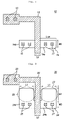
- FIG. 1 is a plan layout view showing a reference transistor for illustrating a structural characteristic of a transistor according to the present invention
- FIG. 2 is a plan layout view illustrating a structure of the transistor according to the present invention.
- FIG. 3 is a plan layout view showing a first comparison transistor compared with the structure of the transistor according to the present invention
- FIG. 4 is a plan layout view showing a second comparison transistor compared with the structure of the transistor according to the present invention.
- FIG. 5 is a plan layout view showing a third comparison transistor compared with the structure of the transistor according to the present invention.
- FIG. 1 is a plan layout view showing a reference transistor for illustrating a structural characteristic of a transistor according to the present invention.
- the transistor shown in FIG. 1 includes a gate conductor 12 and an active area 14 .
- the gate conductor 12 for example, is made of poly-silicon and intersects the active area 14 .
- the active area 14 is an area in which impurities (e.g., N-type impurities such as P, As and N, or P-type impurities such as B, Ga and In) are implanted or diffused onto a semiconductor (e.g., silicon) substrate.
- the active area 14 is divided into source and drain areas 14 s and 14 d with the gate conductor 12 overlapping with the active area 14 as reference.
- the gate conductor 12 is electrically isolated from the active area 14 .
- the gate conductor 12 is connected electrically to the outside (e.g., a gate electrode) through gate contact holes 13 .
- the source and drain areas 14 s and 14 d are connected electrically to the outside through source and drain contact holes 17 and 15 , respectively.
- a bias voltage (a positive (+) voltage in an NMOS transistor or a negative ( ⁇ ) voltage in a PMOS transistor) of a threshold voltage or more is applied to the gate conductor 12 , an electric field is formed with the gate conductor as a center, and a channel (not shown) is formed below the gate insulating layer due to the influence of the electric field. If the channel is formed by a gate voltage, a current flows between the source and drain areas 14 s and 14 d . Since the current does not flow through the channel if the bias voltage is removed, the operation of a transistor can be implemented. Since the transistor includes a semiconductor substrate, a gate insulating layer and a gate conductor, the transistor is referred to as a MOS transistor.
- the MOS transistor 10 of FIG. 1 is a narrow width transistor having a small width W 0 of 0.3 ⁇ m and a channel length L 0 of 0.13 ⁇ m.
- the MOS transistor 10 having such dimension and structure is implemented as NMOS and PMOS transistors, assuming that each driving current of the NMOS and PMOS transistors is 100, the inventor of the present invention has studied a structure of a transistor capable of optimizing the driving current while varying the structure and dimension of the transistor. As a result, it can be seen that a driving current is the most optimally enhanced in the structure and dimension of a transistor shown in FIG. 2 , and both performance enhancements for PMOS and NMOS transistors can be achieved.
- the transistor 20 according to the present invention includes source and drain additional active areas 27 and 29 respectively having the source and drain areas extended in a channel width direction as shown in FIG. 2 .
- the length L 1 of each of the additional active areas 27 and 29 is set to be smaller than that L s/d of each of the source and drain areas 14 s and 14 d of the reference transistor 10 ( FIG. 1 ) such that the channel width itself of the transistor 20 does not increase due to the additional active areas 27 and 29 .
- a difference between L 1 and L s/d is set to be maximal as long as the design rule accepts it.
- the respective additional active areas 27 and 29 are the same areas in which impurities are diffused as the source and drain areas 24 s and 24 d , only the pattern of a mask is modified to include a pattern corresponding to the additional active areas 27 and 29 without utilizing an additional photo mask to form the additional active areas 27 and 29 . That is, in order to form the additional active areas 27 and 29 of the present invention, it is not required to modify a semiconductor manufacturing method or to introduce a new process.
- the width W 1 of each of the additional active areas 27 and 29 is 0.35 ⁇ m, and the length L 1 thereof is 0.3 ⁇ m. That is, the width of each of the additional active areas 27 and 29 according to the present invention is larger than the channel width of the transistor 20 .
- the channel width W 0 and length L 0 of the transistor 20 are the same as those of the reference transistor 10 .
- the driving current of the transistor 20 is represented as 107.27% as compared with that of the reference transistor 10 .
- the driving current is represented as 103.31%.
- the current driving performance of the transistor 20 of the present invention is represented as 103% or more in both PMOS and NMOS transistors as compared with that of the reference transistor 10 so that both performance of the PMOS and NMOS transistors can be simultaneously enhanced.
- the transistor 20 is a MOS transistor in which an active area 24 having the source and drain areas 24 s and 24 d intersects a gate conductor 22 , the gate conductor 22 is connected electrically to the outside through gate contact holes 23 , and the source and drain areas 24 s and 24 d are connected electrically to the outside through source and drain contact holes 27 and 25 , respectively.
- FIG. 3 is a plan layout view showing a first comparison transistor compared with the structure of the transistor according to the present invention.
- the first comparison transistor 30 is a MOS transistor in which an active area 34 having source and drain areas 34 s and 34 d intersects a gate conductor 32 , the gate conductor 32 is connected electrically to the outside through gate contact holes 33 , and the source and drain areas 34 s and 34 d are connected electrically to the outside through source and drain contact holes 37 and 35 , respectively.
- an additional active area is formed at any one of source and drain areas.
- an additional active area 37 is added to the source area 34 s in this figure.
- the width W 1 and length L 1 of the additional active area 37 is identical to the additional active areas 27 and 29 of the transistor 20 according to the present invention.
- the width W 1 of the additional active area 37 is set to be 0.35 ⁇ m
- the channel width and length of the first comparison transistor 30 is set to be identical to the reference transistor 10 .
- the driving current of the first comparison transistor 30 is represented as 101.14% as compared with the reference transistor 10 .
- the driving current is represented as 100.00%, representing no difference between the first comparison transistor 30 and the reference transistor 10 .
- FIG. 4 is a plan layout view showing a second comparison transistor compared with the structure of the transistor according to the present invention.
- the second comparison transistor 40 is a MOS transistor in which an active area 44 having source and drain areas 44 s and 44 d intersects a gate conductor 42 , the gate conductor 42 is connected electrically to the outside through gate contact holes 43 , and the source and drain areas 44 s and 44 d are connected electrically to the outside through source and drain contact holes 47 and 45 , respectively.
- an additional active area is formed at any one of source and drain areas like the first comparison transistor 30 .
- an additional active area 47 is added to the source area 44 s in this figure.
- the width W 2 of the additional active area 47 is smaller than those of the additional active areas 27 and 29 of the transistor 20 according to the present invention.
- the length L 1 of the additional active area 47 is identical to the transistor 20 of the present invention.
- the width W 2 of the additional active area 47 is set to be 0.3 ⁇ m, which is smaller than W 1
- the channel width and length of the second comparison transistor 40 is set to be identical to the reference transistor 10 .
- the driving current of the second comparison transistor 40 is represented as 101.82% as compared with the reference transistor 10 .
- the driving current is represented as 98.90%, which is smaller than that of the reference transistor 10 .
- FIG. 5 is a plan layout view showing a third comparison transistor compared with the structure of the transistor according to the present invention.
- the third comparison transistor 50 is a MOS transistor, like the reference transistor 10 , in which an active area 54 having source and drain areas 54 s and 54 d intersects a gate conductor 52 , the gate conductor 52 is connected electrically to the outside through gate contact holes 53 , and the source and drain areas 54 s and 54 d are connected electrically to the outside through source and drain contact holes 57 and 55 , respectively.
- additional active areas 57 and 59 are respectively formed at both source and drain areas 54 s and 54 d like the transistor 20 of the present invention.
- the width W 2 of each of the additional active areas 57 and 59 is smaller than that W 1 of each of the additional active areas 27 and 29 of the transistor 20 according to the present invention.
- the length L 1 of each of the additional active areas 57 and 59 is identical to the transistor 20 of the present invention.
- the width W 2 of each of the additional active areas 57 and 59 is set to be 0.3 ⁇ m, which is smaller than W 1 , and the channel width and length of the third comparison transistor 50 are set to be identical to the reference transistor 10 .
- the driving current of the third comparison transistor 50 is represented as 100.68% as compared with the reference transistor 10 .
- the driving current is represented as 100.55%, representing little difference between the third comparison transistor 50 and the reference transistor 10 .
- the structure of the transistor 20 according to the present invention is not modified by setting the channel width and length of the transistor 20 to be identical to the reference transistor 10 , and the additional active areas 27 and 29 is added to the transistor 20 , so that the driving currents of both NMOS and PMOS transistors can be enhanced by 103% or more.
- problems with both PMOS and NMOS transistors can be solved because a driving control drops due to a narrow width effect while the channel width of a transistor is reduced.
Abstract
Description
| TABLE 1 | |||||||
| Width of | Length of | NMOS | PMOS | ||||
| Channel | Channel | Additional | Additional | Additional | Driving | Driving | |
| Classification | Width | length | Active Area | Active Area | Active Area | Current | Current |
| Ref Trans. | 0.3 μm | 0.13 μm | None | — | — | 100 | 100 |
| Trans. of present | 0.3 μm | 0.13 μm | 2 | 0.35 μm | 0.3 μm | 107.27% | 103.31% |
| invention | |||||||
| 1st Comparison | 0.3 μm | 0.13 μm | 1 | 0.35 μm | 0.3 μm | 101.14% | 100.0% |
| Trans. | |||||||
| 2nd comparison | 0.3 μm | 0.13 μm | 1 | 0.3 μm | 0.3 μm | 101.82% | 98.90% |
| Trans. | |||||||
| 3rd comparison | 0.3 μm | 0.13 μm | 2 | 0.3 μm | 0.3 μm | 100.68% | 100.55% |
| trans. | |||||||
Claims (20)
Priority Applications (1)
| Application Number | Priority Date | Filing Date | Title |
|---|---|---|---|
| US12/416,042 US7906399B2 (en) | 2005-12-29 | 2009-03-31 | Narrow width metal oxide semiconductor transistor |
Applications Claiming Priority (2)
| Application Number | Priority Date | Filing Date | Title |
|---|---|---|---|
| KR10-2005-0134163 | 2005-12-29 | ||
| KR1020050134163A KR100650867B1 (en) | 2005-12-29 | 2005-12-29 | Narrow width metal oxide semiconductor transistor |
Related Child Applications (1)
| Application Number | Title | Priority Date | Filing Date |
|---|---|---|---|
| US12/416,042 Division US7906399B2 (en) | 2005-12-29 | 2009-03-31 | Narrow width metal oxide semiconductor transistor |
Publications (2)
| Publication Number | Publication Date |
|---|---|
| US20070152244A1 US20070152244A1 (en) | 2007-07-05 |
| US7528455B2 true US7528455B2 (en) | 2009-05-05 |
Family
ID=37713963
Family Applications (2)
| Application Number | Title | Priority Date | Filing Date |
|---|---|---|---|
| US11/646,727 Active 2027-02-14 US7528455B2 (en) | 2005-12-29 | 2006-12-27 | Narrow width metal oxide semiconductor transistor |
| US12/416,042 Active 2027-01-26 US7906399B2 (en) | 2005-12-29 | 2009-03-31 | Narrow width metal oxide semiconductor transistor |
Family Applications After (1)
| Application Number | Title | Priority Date | Filing Date |
|---|---|---|---|
| US12/416,042 Active 2027-01-26 US7906399B2 (en) | 2005-12-29 | 2009-03-31 | Narrow width metal oxide semiconductor transistor |
Country Status (5)
| Country | Link |
|---|---|
| US (2) | US7528455B2 (en) |
| JP (1) | JP2007184582A (en) |
| KR (1) | KR100650867B1 (en) |
| CN (1) | CN100527441C (en) |
| DE (1) | DE102006061172A1 (en) |
Cited By (3)
| Publication number | Priority date | Publication date | Assignee | Title |
|---|---|---|---|---|
| US10748998B2 (en) | 2018-06-22 | 2020-08-18 | Samsung Electronics Co., Ltd. | Semiconductor devices having alternating connecting and separating sections below the gate electrode |
| US10846458B2 (en) * | 2018-08-30 | 2020-11-24 | Taiwan Semiconductor Manufacturing Company Ltd. | Engineering change order cell structure having always-on transistor |
| US20220037316A1 (en) * | 2020-08-03 | 2022-02-03 | Samsung Electronics Co., Ltd. | Semiconductor device and method for fabricating the same |
Families Citing this family (4)
| Publication number | Priority date | Publication date | Assignee | Title |
|---|---|---|---|---|
| US8633077B2 (en) | 2012-02-15 | 2014-01-21 | International Business Machines Corporation | Transistors with uniaxial stress channels |
| JP6258672B2 (en) * | 2013-11-21 | 2018-01-10 | ルネサスエレクトロニクス株式会社 | Manufacturing method of semiconductor device |
| TWI562120B (en) * | 2015-11-11 | 2016-12-11 | Au Optronics Corp | Pixel circuit |
| EP3853898B1 (en) * | 2019-02-27 | 2023-08-02 | Yangtze Memory Technologies Co., Ltd. | Bit line driver device |
Citations (13)
| Publication number | Priority date | Publication date | Assignee | Title |
|---|---|---|---|---|
| US5821600A (en) * | 1994-12-20 | 1998-10-13 | Stmicroelectronics, Inc. | Isolation by active transistors with grounded gates |
| US20020093028A1 (en) * | 1998-11-16 | 2002-07-18 | Akito Konishi | Semiconductor device and a process for manufacturing the same |
| US6476424B1 (en) * | 1999-02-10 | 2002-11-05 | Sony Corporation | Semiconductor memory device |
| US20030042529A1 (en) * | 2001-07-02 | 2003-03-06 | Fujitsu Limited | Non-volatile semiconductor memory device and semiconductor integrated circuit |
| US6692996B2 (en) * | 2000-11-11 | 2004-02-17 | Pt Plus Co., Ltd. | Method for crystallizing silicon layer |
| US6787823B2 (en) * | 2002-07-19 | 2004-09-07 | Renesas Technology Corp. | Semiconductor device having cell-based basic element aggregate having protruding part in active region |
| US20040238897A1 (en) * | 2003-05-30 | 2004-12-02 | Amane Oishi | MOS semiconductor device |
| US20050093019A1 (en) * | 2003-10-31 | 2005-05-05 | Semiconductor Energy Laboratory Co., Ltd. | Transistor |
| US6933578B2 (en) * | 2003-06-11 | 2005-08-23 | Seiko Epson Corporation | Semiconductor storage device |
| US20060006474A1 (en) * | 2004-07-12 | 2006-01-12 | Nobuo Tsuboi | Semiconductor device |
| US7064453B2 (en) * | 2003-06-11 | 2006-06-20 | Seiko Epson Corporation | Semiconductor memory device including a gate electrode with a recess |
| US7093215B2 (en) * | 2003-02-05 | 2006-08-15 | Matsushita Electric Industrial Co., Ltd. | Semiconductor circuit device and circuit simulation method for the same |
| US7105901B1 (en) * | 1998-01-29 | 2006-09-12 | Renesas Technology Corp. | Semiconductor device |
Family Cites Families (21)
| Publication number | Priority date | Publication date | Assignee | Title |
|---|---|---|---|---|
| US4224633A (en) * | 1978-05-23 | 1980-09-23 | Fujitsu Limited | IGFET structure with an extended gate electrode end |
| US4622735A (en) * | 1980-12-12 | 1986-11-18 | Tokyo Shibaura Denki Kabushiki Kaisha | Method for manufacturing a semiconductor device utilizing self-aligned silicide regions |
| JPH0828431B2 (en) * | 1986-04-22 | 1996-03-21 | 日本電気株式会社 | Semiconductor memory device |
| JPH0620133B2 (en) * | 1987-05-28 | 1994-03-16 | 宮城工業高等専門学校長 | MOSFET device |
| JP2676819B2 (en) * | 1988-09-20 | 1997-11-17 | ソニー株式会社 | Field effect transistor and semiconductor integrated circuit device |
| JPH02196468A (en) * | 1989-01-25 | 1990-08-03 | Nec Corp | Semiconductor device |
| JP2978504B2 (en) * | 1989-04-14 | 1999-11-15 | 日本電気株式会社 | MOS transistor |
| US5270565A (en) * | 1989-05-12 | 1993-12-14 | Western Digital Corporation | Electro-static discharge protection circuit with bimodal resistance characteristics |
| JPH0389555A (en) * | 1989-09-01 | 1991-04-15 | Hitachi Ltd | Semiconductor device and manufacture thereof |
| JP2894391B2 (en) * | 1991-09-20 | 1999-05-24 | 三菱電機株式会社 | Thin film transistor and method of manufacturing the same |
| US5451799A (en) * | 1992-12-28 | 1995-09-19 | Matsushita Electric Industrial Co., Ltd. | MOS transistor for protection against electrostatic discharge |
| JPH07226446A (en) * | 1994-02-12 | 1995-08-22 | Toshiba Corp | Semiconductor device and its manufacture |
| KR100203900B1 (en) * | 1996-06-24 | 1999-06-15 | 김영환 | Semiconductor device with esd protection circuit |
| TW302539B (en) * | 1996-08-26 | 1997-04-11 | Lin Horng Hyh | Manufacturing method of deep submicron PMOS device shallow junction |
| JP2000124331A (en) * | 1998-10-20 | 2000-04-28 | Matsushita Electric Ind Co Ltd | Semiconductor memory |
| JP2001185721A (en) * | 1999-12-22 | 2001-07-06 | Nec Corp | Semiconductor device |
| JP2002184979A (en) * | 2000-12-19 | 2002-06-28 | Toshiba Corp | Semiconductor device and manufacturing method thereof |
| JP4790166B2 (en) * | 2001-07-05 | 2011-10-12 | Okiセミコンダクタ株式会社 | Protection transistor |
| KR100463203B1 (en) * | 2002-12-10 | 2004-12-23 | 삼성전자주식회사 | A semiconductor device having an active region |
| US7075127B2 (en) * | 2004-01-29 | 2006-07-11 | Infineon Technologies Ag | Single-poly 2-transistor based fuse element |
| US6856031B1 (en) * | 2004-02-03 | 2005-02-15 | International Business Machines Corporation | SRAM cell with well contacts and P+ diffusion crossing to ground or N+ diffusion crossing to VDD |
-
2005
- 2005-12-29 KR KR1020050134163A patent/KR100650867B1/en not_active IP Right Cessation
-
2006
- 2006-12-19 JP JP2006341044A patent/JP2007184582A/en active Pending
- 2006-12-22 DE DE102006061172A patent/DE102006061172A1/en not_active Withdrawn
- 2006-12-25 CN CNB2006101701930A patent/CN100527441C/en not_active Expired - Fee Related
- 2006-12-27 US US11/646,727 patent/US7528455B2/en active Active
-
2009
- 2009-03-31 US US12/416,042 patent/US7906399B2/en active Active
Patent Citations (13)
| Publication number | Priority date | Publication date | Assignee | Title |
|---|---|---|---|---|
| US5821600A (en) * | 1994-12-20 | 1998-10-13 | Stmicroelectronics, Inc. | Isolation by active transistors with grounded gates |
| US7105901B1 (en) * | 1998-01-29 | 2006-09-12 | Renesas Technology Corp. | Semiconductor device |
| US20020093028A1 (en) * | 1998-11-16 | 2002-07-18 | Akito Konishi | Semiconductor device and a process for manufacturing the same |
| US6476424B1 (en) * | 1999-02-10 | 2002-11-05 | Sony Corporation | Semiconductor memory device |
| US6692996B2 (en) * | 2000-11-11 | 2004-02-17 | Pt Plus Co., Ltd. | Method for crystallizing silicon layer |
| US20030042529A1 (en) * | 2001-07-02 | 2003-03-06 | Fujitsu Limited | Non-volatile semiconductor memory device and semiconductor integrated circuit |
| US6787823B2 (en) * | 2002-07-19 | 2004-09-07 | Renesas Technology Corp. | Semiconductor device having cell-based basic element aggregate having protruding part in active region |
| US7093215B2 (en) * | 2003-02-05 | 2006-08-15 | Matsushita Electric Industrial Co., Ltd. | Semiconductor circuit device and circuit simulation method for the same |
| US20040238897A1 (en) * | 2003-05-30 | 2004-12-02 | Amane Oishi | MOS semiconductor device |
| US7064453B2 (en) * | 2003-06-11 | 2006-06-20 | Seiko Epson Corporation | Semiconductor memory device including a gate electrode with a recess |
| US6933578B2 (en) * | 2003-06-11 | 2005-08-23 | Seiko Epson Corporation | Semiconductor storage device |
| US20050093019A1 (en) * | 2003-10-31 | 2005-05-05 | Semiconductor Energy Laboratory Co., Ltd. | Transistor |
| US20060006474A1 (en) * | 2004-07-12 | 2006-01-12 | Nobuo Tsuboi | Semiconductor device |
Cited By (5)
| Publication number | Priority date | Publication date | Assignee | Title |
|---|---|---|---|---|
| US10748998B2 (en) | 2018-06-22 | 2020-08-18 | Samsung Electronics Co., Ltd. | Semiconductor devices having alternating connecting and separating sections below the gate electrode |
| US10846458B2 (en) * | 2018-08-30 | 2020-11-24 | Taiwan Semiconductor Manufacturing Company Ltd. | Engineering change order cell structure having always-on transistor |
| US11275885B2 (en) | 2018-08-30 | 2022-03-15 | Taiwan Semiconductor Manufacturing Company, Ltd. | Engineering change order cell structure having always-on transistor |
| US11675961B2 (en) | 2018-08-30 | 2023-06-13 | Taiwan Semiconductor Manufacturing Company, Ltd. | Engineering change order cell structure having always-on transistor |
| US20220037316A1 (en) * | 2020-08-03 | 2022-02-03 | Samsung Electronics Co., Ltd. | Semiconductor device and method for fabricating the same |
Also Published As
| Publication number | Publication date |
|---|---|
| CN100527441C (en) | 2009-08-12 |
| US7906399B2 (en) | 2011-03-15 |
| JP2007184582A (en) | 2007-07-19 |
| KR100650867B1 (en) | 2006-11-28 |
| CN1992343A (en) | 2007-07-04 |
| DE102006061172A1 (en) | 2007-08-16 |
| US20070152244A1 (en) | 2007-07-05 |
| US20090186461A1 (en) | 2009-07-23 |
Similar Documents
| Publication | Publication Date | Title |
|---|---|---|
| US7906399B2 (en) | Narrow width metal oxide semiconductor transistor | |
| KR100460553B1 (en) | A method of manufacturing an insulated gate semiconductor device | |
| JP3364559B2 (en) | Semiconductor device | |
| US6919606B2 (en) | Semiconductor device comprising an insulating mask formed on parts of a gate electrode and semiconductor layer crossing an active region | |
| JP3110262B2 (en) | Semiconductor device and operating method of semiconductor device | |
| US20070241426A1 (en) | Semiconductor device | |
| US7279767B2 (en) | Semiconductor structure with high-voltage sustaining capability and fabrication method of the same | |
| KR100231717B1 (en) | Semiconductor device and method of fabricating the same | |
| JP2010087436A (en) | Semiconductor device | |
| US20050184361A1 (en) | Vertical bipolar transistor and method of manufacturing the same | |
| US8102011B2 (en) | Semiconductor device including a field effect transistor and method for manufacturing the same | |
| US7091535B2 (en) | High voltage device embedded non-volatile memory cell and fabrication method | |
| JP2011210901A (en) | Depression-type mos transistor | |
| US6476430B1 (en) | Integrated circuit | |
| JPH08330528A (en) | Semiconductor storage and its manufacture | |
| US20020050618A1 (en) | Semiconductor device and manufacturing method thereof | |
| US20070152281A1 (en) | Narrow width metal oxide semiconductor transistor having a supplemental gate conductor pattern | |
| JPH05283626A (en) | Semiconductor integrated circuit device | |
| US6130133A (en) | Fabricating method of high-voltage device | |
| US5610428A (en) | Semiconductor integrated circuit | |
| US11532629B1 (en) | Bent gate logic device | |
| KR100505627B1 (en) | Method of manufacturing CMOS transistor selectively using OPC | |
| US20240105844A1 (en) | Native nmos device and manufacturing method thereof | |
| JPH0786582A (en) | Semiconductor device | |
| JPH11220124A (en) | Semiconductor device |
Legal Events
| Date | Code | Title | Description |
|---|---|---|---|
| AS | Assignment |
Owner name: DONGBU ELECTRONICS CO., LTD., KOREA, REPUBLIC OF Free format text: ASSIGNMENT OF ASSIGNORS INTEREST;ASSIGNOR:AHN, JUNG HO;REEL/FRAME:018742/0489 Effective date: 20061227 |
|
| FEPP | Fee payment procedure |
Free format text: PAYER NUMBER DE-ASSIGNED (ORIGINAL EVENT CODE: RMPN); ENTITY STATUS OF PATENT OWNER: LARGE ENTITY Free format text: PAYOR NUMBER ASSIGNED (ORIGINAL EVENT CODE: ASPN); ENTITY STATUS OF PATENT OWNER: LARGE ENTITY |
|
| FEPP | Fee payment procedure |
Free format text: PAYOR NUMBER ASSIGNED (ORIGINAL EVENT CODE: ASPN); ENTITY STATUS OF PATENT OWNER: LARGE ENTITY |
|
| STCF | Information on status: patent grant |
Free format text: PATENTED CASE |
|
| FPAY | Fee payment |
Year of fee payment: 4 |
|
| FEPP | Fee payment procedure |
Free format text: PAT HOLDER CLAIMS SMALL ENTITY STATUS, ENTITY STATUS SET TO SMALL (ORIGINAL EVENT CODE: LTOS); ENTITY STATUS OF PATENT OWNER: LARGE ENTITY |
|
| FEPP | Fee payment procedure |
Free format text: PAYER NUMBER DE-ASSIGNED (ORIGINAL EVENT CODE: RMPN); ENTITY STATUS OF PATENT OWNER: LARGE ENTITY Free format text: PAYOR NUMBER ASSIGNED (ORIGINAL EVENT CODE: ASPN); ENTITY STATUS OF PATENT OWNER: LARGE ENTITY |
|
| AS | Assignment |
Owner name: INPHI CORPORATION, UNITED STATES Free format text: ASSIGNMENT OF ASSIGNORS INTEREST;ASSIGNOR:DONGBU HITEK, CO., LTD.;REEL/FRAME:034009/0157 Effective date: 20141008 |
|
| AS | Assignment |
Owner name: INPHI CORPORATION, CALIFORNIA Free format text: CORRECTIVE ASSIGNMENT TO CORRECT REMOVE PATENT NO. 878209 FROM EXHIBIT B PREVIOUSLY RECORDED AT REEL: 034009 FRAME: 0157. ASSIGNOR(S) HEREBY CONFIRMS THE ASSIGNMENT;ASSIGNOR:DONGBU HITEK, CO., LTD.;REEL/FRAME:034087/0097 Effective date: 20141008 |
|
| FEPP | Fee payment procedure |
Free format text: PAYER NUMBER DE-ASSIGNED (ORIGINAL EVENT CODE: RMPN); ENTITY STATUS OF PATENT OWNER: LARGE ENTITY Free format text: PAYOR NUMBER ASSIGNED (ORIGINAL EVENT CODE: ASPN); ENTITY STATUS OF PATENT OWNER: LARGE ENTITY |
|
| FPAY | Fee payment |
Year of fee payment: 8 |
|
| AS | Assignment |
Owner name: INPHI CORPORATION, CALIFORNIA Free format text: ASSIGNMENT OF ASSIGNORS INTEREST;ASSIGNOR:DONGBU HITEK, CO., LTD.;REEL/FRAME:041446/0982 Effective date: 20141008 |
|
| FEPP | Fee payment procedure |
Free format text: ENTITY STATUS SET TO UNDISCOUNTED (ORIGINAL EVENT CODE: BIG.) |
|
| MAFP | Maintenance fee payment |
Free format text: PAYMENT OF MAINTENANCE FEE, 12TH YEAR, LARGE ENTITY (ORIGINAL EVENT CODE: M1553); ENTITY STATUS OF PATENT OWNER: LARGE ENTITY Year of fee payment: 12 |
|
| AS | Assignment |
Owner name: MARVELL TECHNOLOGY CAYMAN I, CAYMAN ISLANDS Free format text: ASSIGNMENT OF ASSIGNORS INTEREST;ASSIGNOR:INPHI CORPORATION;REEL/FRAME:056649/0823 Effective date: 20210617 |
|
| AS | Assignment |
Owner name: CAVIUM INTERNATIONAL, CAYMAN ISLANDS Free format text: ASSIGNMENT OF ASSIGNORS INTEREST;ASSIGNOR:MARVELL TECHNOLOGY CAYMAN I;REEL/FRAME:057279/0519 Effective date: 20210620 |
|
| AS | Assignment |
Owner name: MARVELL ASIA PTE LTD., SINGAPORE Free format text: ASSIGNMENT OF ASSIGNORS INTEREST;ASSIGNOR:CAVIUM INTERNATIONAL;REEL/FRAME:057336/0873 Effective date: 20210620 |