US7542646B2 - Optical waveguide and method of manufacturing the same - Google Patents
Optical waveguide and method of manufacturing the same Download PDFInfo
- Publication number
- US7542646B2 US7542646B2 US12/033,039 US3303908A US7542646B2 US 7542646 B2 US7542646 B2 US 7542646B2 US 3303908 A US3303908 A US 3303908A US 7542646 B2 US7542646 B2 US 7542646B2
- Authority
- US
- United States
- Prior art keywords
- curable resin
- cavity
- cladding
- waveguide core
- core
- Prior art date
- Legal status (The legal status is an assumption and is not a legal conclusion. Google has not performed a legal analysis and makes no representation as to the accuracy of the status listed.)
- Expired - Fee Related
Links
Images


Classifications
-
- G—PHYSICS
- G02—OPTICS
- G02B—OPTICAL ELEMENTS, SYSTEMS OR APPARATUS
- G02B6/00—Light guides; Structural details of arrangements comprising light guides and other optical elements, e.g. couplings
- G02B6/10—Light guides; Structural details of arrangements comprising light guides and other optical elements, e.g. couplings of the optical waveguide type
- G02B6/12—Light guides; Structural details of arrangements comprising light guides and other optical elements, e.g. couplings of the optical waveguide type of the integrated circuit kind
- G02B6/122—Basic optical elements, e.g. light-guiding paths
- G02B6/125—Bends, branchings or intersections
-
- G—PHYSICS
- G02—OPTICS
- G02B—OPTICAL ELEMENTS, SYSTEMS OR APPARATUS
- G02B6/00—Light guides; Structural details of arrangements comprising light guides and other optical elements, e.g. couplings
- G02B6/10—Light guides; Structural details of arrangements comprising light guides and other optical elements, e.g. couplings of the optical waveguide type
- G02B6/12—Light guides; Structural details of arrangements comprising light guides and other optical elements, e.g. couplings of the optical waveguide type of the integrated circuit kind
- G02B6/13—Integrated optical circuits characterised by the manufacturing method
- G02B6/138—Integrated optical circuits characterised by the manufacturing method by using polymerisation
Definitions
- the present invention relates to an optical waveguide and a method of manufacturing the same.
- an optical waveguide including: a waveguide core through which light propagates; a cavity that is present inside the waveguide core so as to be open at least one end in the thickness direction of the waveguide core; a layer-form first cladding having a lower refractive index than the waveguide core, and sealing at least one of the opening(s) of the cavity to thereby close the opening of the cavity; and a second cladding having a lower refractive index than the waveguide core, and surrounding the waveguide core.
- FIG. 1 is a perspective view showing an optical waveguide according to an exemplary embodiment
- FIG. 2 is a plan view showing the optical waveguide according to the exemplary embodiment
- FIG. 3 is a partial cross-sectional view showing the optical waveguide according to the exemplary embodiment
- FIGS. 4A to 4E are process views showing a process of manufacturing the optical waveguide according to the exemplary embodiment
- FIGS. 5A to 5F are process views showing the process of manufacturing the optical waveguide according to the exemplary embodiment
- FIG. 6 is a perspective view showing an optical waveguide according to another exemplary embodiment
- FIG. 7 is a plan view showing the optical waveguide according to another exemplary embodiment.
- FIG. 8 is a partial cross-sectional view showing the optical waveguide according to another exemplary embodiment.
- FIG. 1 is a perspective view showing an optical waveguide according to the exemplary embodiment.
- FIG. 2 is a plan view showing the optical waveguide according to the exemplary embodiment.
- FIG. 3 is a partial cross-sectional view showing the optical waveguide according to the exemplary embodiment, taken along the line A-A of FIG. 2 .
- the optical waveguide 10 includes a lower cladding substrate 12 (first substrate) and an upper cladding substrate 14 (second substrate). Between the substrates 12 and 14 , a waveguide core 16 propagating light and a second cladding 20 formed so as to surround the waveguide core 16 are provided.
- the waveguide core 16 includes two main waveguide cores 16 A and 16 B coupled so as to cross each other (in the present exemplary embodiment, at a right angle) at one ends thereof to form an L-shape.
- a cavity 22 is disposed in the part where the main waveguide cores 16 A and 16 B are coupled together.
- the cavity 22 is constituted by a space surrounded by the waveguide core 16 .
- the cavity 22 is open on both of the side facing the lower cladding substrate 12 (first substrate) and the side facing the upper cladding substrate 14 (second substrate) (that is, open in both of the directions along the thickness of the waveguide core 16 ).
- the opening on the side of the lower cladding substrate 12 is sealed by being sealed by the lower cladding substrate 12 .
- the opening on the side of the upper cladding substrate 14 is sealed by a layer-form first cladding 18 . It is to be noted that the first cladding 18 may seal the opening on the side of the lower cladding substrate 12 by sealing it.
- the first cladding 18 is formed in a layer form on the entire area of the upper cladding substrate 14 having the same size as the lower cladding substrate 12 in order to close the opening on the side of the upper cladding substrate 14 and covers the entire area of the waveguide core 16 and the second cladding 20
- the present invention is not limited thereto.
- the first cladding 18 may be formed in a layer form on the entire area of the upper cladding substrate 14 of a size sealing only a peripheral area of the opening so as to cover only the peripheral area of the opening.
- the first cladding 18 be formed of the same material as the second cladding 20 , it may be formed of a different material.
- the inclined surface in the cavity 22 inclined with respect to the direction of the propagating light through the main waveguide cores 16 A and 16 B serves as a reflecting surface 22 A because of the difference in refractive index between the waveguide core 16 and the cavity 22 . That is, the propagating light incident from the incident side 16 C of the main waveguide core 16 A reaches the cavity 22 , is reflected at the reflecting surface 22 A (inclined surface) in the cavity 22 , propagates through the main waveguide core 16 B, and exits from the exit side 16 D.
- the cavity 22 the reflection angle and reflection amount of which are optically set is present inside the waveguide core 16 , the boundary between the cavity 22 and the waveguide core 16 serves as the reflecting surface, and a change of the propagation direction is realized using the fact that the difference in refractive index between the core and the medium (gas) in the cavity 22 is comparatively large.
- the cavity 22 is regarded as a local gas cladding in the waveguide core 16 .
- the refractive index of the waveguide core 16 is 1.5 and the gas in the cavity 22 is air, a total reflection of up to 41.8 degrees with reference to the normal to the reflecting surface (93.2 degrees with reference to the propagation direction) can be realized.
- the critical angle with respect to the normal to the reflecting surface 22 A is approximately 40 degrees, and when the angle of the reflecting surface with respect to the propagation direction is 45 degrees, total reflection is possible, so that the propagation direction can be changed by 90 degrees.
- NA numerical aperture
- the area (reflection effective area) of the overlapping part of the cross section of the main waveguide core 16 A and the projection when the reflecting surface 22 A is projected in the light propagation direction of the main waveguide core 16 A is the same as the cross-sectional area of the main waveguide core 16 A.
- the effective reflecting surface is the same as the core size when viewed from the incident side, the light propagating through the main waveguide core 16 A has its propagation direction changed at the reflecting surface by total reflection.
- the propagation light is reflected at the reflecting surface 22 A at an angle same with or extremely close to the angle of total reflection, the light is branched into totally reflected light and partially transmitted light, so that a branching waveguide can also be realized.
- a branching waveguide can be realized that branches the propagating light incident on the main waveguide core 16 A into light reflected at the reflecting surface 22 A and light propagating through the part of the main waveguide core 16 A other than the reflecting surface 22 A to propagate in a straight line.
- the light reflecting on the surface has its propagation direction changed by reflection, and the light not reflecting propagates through the main waveguide core without its direction changed, so that a wide branching angle waveguide can be realized.
- the cavity 22 is present inside the waveguide core 16 , and the propagation direction is changed with the boundary between the waveguide core 16 and the cavity 22 as the reflecting surface. That is, since the reflecting surface 22 A constituted by the boundary between the waveguide core 16 and the cavity 22 where a gas is enclosed is provided inside the waveguide core 16 , the propagation direction is changed locally and in a space-saving manner in a given position in the waveguide core 16 .
- the cavity 22 is formed without any foreign matter entering therein when the optical waveguide is manufactured. Consequently, an excellent reflecting surface is formed, so that an optical waveguide with a stable reflection characteristic is provided.
- optical waveguide 10 it is preferable that the optical waveguide 10 according to the present exemplary embodiment be used in the multimode.
- the method of manufacturing the optical waveguide according to the exemplary embodiment includes, for example, the following steps 1) to 6):
- FIGS. 4A to 4E and 5 A to 5 F are process schematic views showing the method of manufacturing the optical waveguide according to the exemplary embodiment.
- the waveguide core 16 through which light propagates and the cavity 22 opened (in the present exemplary embodiment, one opening is closed by the lower cladding substrate 12 and the other is opened) on the surface opposite to the surface of the first substrate in the waveguide core 16 in the direction of thickness thereof are formed on the first substrate (in the present exemplary embodiment, the lower cladding substrate 12 ) (see FIG. 4A ).
- the cavity 22 is present inside the waveguide core 16 , and with a part or the entire area of the boundary with the waveguide core 16 as the reflecting surface 22 A, the direction of the propagating light is partly or wholly changed.
- the step 1) includes, for example, the following steps a) to e):
- the cavity 22 is formed simultaneously with the formation of the waveguide core 16 without the need for providing another step such as etching and equipment, therefore, manufacture is easy. Moreover, since in the step 1), the surface serving as the reflecting surface in the cavity 22 depends on the precision and flatness of the surface of the mold 24 corresponding to the cavity 22 , the precision of the reflecting surface is easily improved by improving the surface precision and flatness of the mold 24 .
- step 1) that is, the steps a) to e) will be described in the following:
- the mold 24 is prepared that is formed of a curable resin layer of a mold-forming curing resin and has the core-forming concave portion 24 A corresponding to the waveguide core and the cavity-forming convex portion 24 B corresponding to the cavity 22 .
- the mold 24 may be formed by using a master 26 where a convex portion 26 A corresponding to the waveguide core 16 and a concave portion 26 B corresponding to the cavity 22 are formed, the present invention is not limited thereto. In the following, a method using the master 26 will be described.
- the convex portion 26 A corresponding to the waveguide core 16 and the concave portion 26 B corresponding to the cavity 22 are formed on a substrate 26 C (see FIG. 5A ).
- a conventional method such as photolithography is used without any particular limitation.
- a method of manufacturing a polymer optical waveguide by an electrodeposition method or an optical electrodeposition method JP-A No. 2002-333538, is also applicable to the fabrication of the master.
- the size of the convex portion corresponding to the waveguide core formed in the master depends on the use of the polymer optical waveguide or the like.
- a waveguide core of approximately 10 ⁇ m square is used in the case of single-mode optical waveguides and a waveguide core of approximately not less than 50 ⁇ m and not more than 100 ⁇ m square is used in the case of multimode optical waveguides
- an optical waveguide having a larger waveguide core of approximately several hundreds ⁇ m square is also used for some uses.
- application to an optical waveguide having a larger waveguide core of approximately several hundreds ⁇ m square is possible.
- the size of the convex portion 26 A corresponding to these waveguide cores can be set irrespective of the size of the concave portion 26 B corresponding to the cavity 22 .
- the mold-forming curable resin is applied to or casted on the surface of the formed master 26 where the convex portion 26 A corresponding to the waveguide core 16 and the concave portion 26 B corresponding to the cavity 22 are formed, and after left for a predetermined time, the resin is vacuum degassed for ten minutes to form a mold-forming curable resin layer 24 C (see FIG. 5B ). After dried as required, the resin is cured. Then, the mold-forming curable resin layer 24 C is detached from the master 26 to form the mold 24 where the core-forming concave portion 24 A and the cavity-forming convex portion 24 B are provided (see FIG. 5C ).
- an inlet for filling the core-forming curable resin into the core-forming concave portion 24 A and an outlet for discharging the resin from the core-forming concave portion 24 A are formed (not shown), and their forming method is not specifically limited. While convex portions corresponding to the inlet and the outlet may be previously provided in the master 26 , an example of a simple method is as follows: The mold-forming curable resin layer 24 C is formed on the master 26 and separated therefrom to form the mold. Then, both ends of the mold are cut so that the core-forming concave portion 24 A is exposed to thereby form the inlet and the outlet.
- the thickness of the mold-forming curable resin layer 24 C is determined in consideration of handleability as the mold 24 , and its appropriate value is generally approximately not less than 0.1 mm and not more than 50 mm. Moreover, mold releasing processing such as application of a mold releasing agent may be previously performed on the master 26 to promote detaching from the mold.
- the mold-forming curable resin it is preferable for the mold-forming curable resin to be easily detached from the master 26 when cured, have a mechanical strength and a dimensional stability of not less than a predetermined level when formed into the mold 24 (repetitively used), have a hardness that maintains the concave and convex shapes, and is excellent in the adhesion to the lower cladding substrate.
- Various kinds of additives may be added to the mold-forming curable resin as required.
- the mold-forming curable resin may have a viscosity of not more than a certain limit, for example, approximately not less than 500 mPa ⁇ s and not more than 7000 mPa ⁇ s since it can be applied to or casted on the surface of the master 26 and it is necessary to precisely copy the convex portion 26 A corresponding to each waveguide core 16 and the concave portion 26 B corresponding to the cavity 22 formed on the master 26 (the “mold-forming curable resin” used in the present invention includes one that becomes a gummous form having elasticity after cured).
- a solvent may be added to an extent that no adverse effect is produced by the solvent, to adjust the viscosity.
- curing organopolysiloxane that becomes silicone rubber (silicone elastomer) or silicone resin after cured may be used from the viewpoint of separatability, mechanical strength, dimensional stability, hardness, and the adhesion to the lower cladding substrate as mentioned above.
- the above-mentioned curing organopolysiloxane may be one including a methylsiloxane group, an ethylsiloxane group, and a phenylsiloxane group in its molecules.
- the above-mentioned curing organopolysiloxane may be either one-component type or two-component type used in combination with a curing agent, may be either a thermosetting type or a room temperature setting type (for example, one cured by moisture in the air at room temperature (for example, 25° C.)), or may be one using a different type of curing (ultraviolet curing, etc.).
- the curing organopolysiloxane be one that becomes silicone rubber after cured.
- liquid silicone rubber (“liquid” includes one having high viscosity such as paste) is normally used, and a two-component type used in combination with a curing agent is preferable.
- addition type liquid silicone rubber is preferably used because unevenness is suppressed in its surface and inside and it is hardened in a short time, produces no or little by-product when hardened, is excellent in mold releasability, and is low in shrinkage factor.
- liquid dimethylsiloxane rubber is particularly preferable from the viewpoint of adhesion, detaching, strength, and hardness.
- the viscosity of the liquid silicone rubber is preferably approximately not less than 500 mPa ⁇ s and not more than 7000 mPa ⁇ s, more preferably approximately not less than 2000 mPa ⁇ s and not more than 5000 mPa ⁇ s.
- the surface energy of the mold 24 be in a range of not less than 10 dyn/cm and not more than 30 dyn/cm, preferably in a range of not less than 15 dyn/cm and not more than 24 dyn/cm from the viewpoint of the adhesion to the substrate.
- the share rubber hardness of the mold 24 be not less than 15 and not more than 80, preferably not less than 20 and not more than 60 from the viewpoint of molding performance, the maintenance of the concave shape, and separatability.
- the surface roughness (root mean square roughness (RMS)) of the mold 24 be not more than 0.2 ⁇ m, preferably not more than 0.1 ⁇ m from the viewpoint of copying performance.
- the mold 24 may transmit light in the ultraviolet region and/or the visible region.
- the mold 24 may transmit light in the visible region because positioning is easy when the mold 24 is brought into close contact with the lower cladding substrate 12 in the following step 2), filling the core-forming curable resin into the core-forming concave portion 24 A of the mold 24 can be observed and the completion of filling and the like can be easily confirmed in the following step 3).
- the mold 24 may transmit light in the ultraviolet region in order to perform ultraviolet curing through the mold 24 when an ultraviolet curable resin is used as the core-forming curable resin.
- the transmittance of the mold 24 in the ultraviolet region (not less than 250 nm and not more than 400 nm) may be not less than 80%.
- liquid silicone rubber that becomes silicone rubber after cured is excellent in mutually contradictory characteristics of adhesion and separatability to and from the lower cladding substrate, is capable of copying nanostructures, and even prevents the entrance of liquid when silicone rubber and the lower cladding substrate 12 are in close contact with each other.
- the mold 24 using this silicone rubber copies the master with high precision and is excellent in adhesion to the lower cladding substrate 12 , the boundary serving as the reflecting surface between the waveguide core 16 and the cavity 22 and the side surface (the boundary with the surrounding cladding) of the waveguide core 16 are extremely excellent, the core-forming resin can be efficiently filled only in the core-forming concave portion 24 A between the mold 24 and the lower cladding substrate 12 , and the lower cladding substrate 12 is easily detached from the mold. Consequently, a polymer optical waveguide the shape of which is highly precisely maintained can be extremely easily formed by using the mold 24 .
- part of the mold-forming curable resin layer 24 C that is, the part other than the part that copies the convex portion 26 A and the concave portion 26 B of the master 26 may be replaced with a different rigid material. In this case, the handleability of the mold 24 is improved.
- the lower cladding substrate 12 (cladding substrate) is brought into close contact with the mold 24 (see FIG. 5D ).
- the material of the lower cladding substrate 12 is selected in consideration of optical characteristic such as refractive index and light transmittance, mechanical strength, thermal stability, flexibility, and the like of the material according to the use.
- a polymer optical waveguide having flexibility may be formed by using a flexible film substrate.
- Examples of the material of the film include acrylic resin (polymethyl methacrylate, etc.), alicyclic acrylic resin, styrene resin (polystyrene, acrylonitrile-styrene copolymer, etc.), olefin resin (polyethylene, polypropylene, ethylene-propylene copolymer, etc.), alicyclic olefin resin, vinyl chloride resin, vinylidene chloride resin, vinyl alcohol resin, vinyl butyral resin, arylate resin, fluorine-containing resin, polyester resin (polyethylene terephthalate, polyethylene naphthalate, etc.), polycarbonate resin, cellulose diacetate or triacetate, amide resin (aliphatic or aromatic polyamide, etc.), imide resin, sulfone resin, polyether sulfone resin, polyetherether ketone resin, polyphenylene sulfide resin, polyoxymethylene resin, and blends of resins mentioned above.
- acrylic resin polymethyl me
- alicyclic acrylic resin OZ-1000, OZ-1100 (manufactured by Hitachi Chemical Co., Ltd.), or the like in which an aliphatic cyclic hydrocarbon such as tricyclodecane is introduced into an ester substituent is used.
- examples of the alicyclic olefin resin include one having a norbornene structure in its main chain and one having a norbornene structure in its main chain and having a polar group such as alkyloxycarbonyl group (as the alkyl group, one with carbon numbers 1 to 6 and cycloalkyl group) in its side chain.
- the alicyclic olefin resin having a norbornene structure in its main chain and having a polar group such as alkyloxycarbonyl group in its side chain as mentioned above is particularly suitable for the formation of the polymer optical waveguide of the present invention because it has excellent optical characteristics such as low refractive index (the refractive index is in the vicinity of 1.50 and the difference in refractive index between the core and the cladding is secured) and light transmittance, is excellent in the adhesion to the mold, and is excellent in thermal resistance.
- the refractive index of the lower cladding substrate 12 be lower than 1.55, preferably lower than 1.53.
- a substrate with cladding in which another substrate is coated with a cladding material is usable. In this case, the flatness of the substrate is improved.
- a material unsuitable as a cladding material because of its high birefringence and a material inferior in transparency are also usable.
- the core-forming curable resin is filled in the core-forming concave portion 24 A of the mold 24 with which the lower cladding substrate 12 is in close contact.
- the core-forming curable resin is filled in the core-forming concave portion 24 A other than the cavity-forming convex portion 24 B of the mold 24 corresponding to the cavity 22 , by a capillary action from the inlet of the mold 24 , and the core-forming curable resin filled in the core-forming concave portion 24 A is discharged from the outlet.
- the core-forming curable resin resins such as radiation curing resin, electron beam curing resin, and thermosetting resin are usable. Among them, ultraviolet curing resin and thermosetting resin are preferably used.
- the ultraviolet curing resin or the thermosetting resin for forming the core an ultraviolet curing or thermosetting monomer or oligomer, or a mixture of a monomer and an oligomer is preferably used.
- the ultraviolet curing resin epoxy, polyimide, or acrylic ultraviolet curing resin is preferably used.
- the core-forming curable resin is filled in the cavity formed between the mold 24 and the lower cladding substrate 12 (the core-forming concave portion 24 A of the mold 24 ) by a capillary action, it is necessary that the core-forming curable resin being used be sufficiently low in viscosity. Therefore, it is preferable that the viscosity of the curable resin be not less than 10 mPa ⁇ s and not more than 2000 mPa ⁇ s, preferably not less than 20 mPa ⁇ s and not more than 1000 mPa ⁇ s, more preferably not less than 30 mPa ⁇ s and not more than 500 mPa ⁇ s.
- the volume change before and after curing of the core-forming curable resin be small.
- the core-forming curable resin may be small in volume change, and it is preferable that the volume change be not more than 10%, preferably not more than 6%.
- the use of a solvent to reduce viscosity is avoided if possible because it results in a large volume change before and after curing.
- a polymer may be added to the core-forming curable resin in order to reduce the volume change (shrinkage) after curing.
- the polymer may be one being miscible with the core-forming curable resin and not adversely affecting the refractive index, elasticity, and transmission characteristic of the resin.
- the viscosity and the glass transition point of the curable resin are highly controlled as well as the volume change is reduced. While an acrylic, methacrylic acid, or epoxy polymer, for example, is used as the polymer, the present invention is not limited thereto.
- the refractive index of the core-forming curable resin when the resin is cured be higher than that of the substrate serving as cladding, and the refractive index is not less than 1.50, preferably not less than 1.53.
- the difference in refractive index between the cladding (including the cladding layer in the following step d)) and the waveguide core is not less than 0.01, preferably not less than 0.03.
- the entire system may be decompressed (approximately not less than 0.1 Pa and not more than 200 Pa), or sucked by using a through hole.
- the filled core-forming curable resin is cured by heat or light.
- the waveguide core 16 is formed (see FIG. 5E ).
- ultraviolet curable resin an ultraviolet lamp, an ultraviolet LED, or an ultraviolet radiation apparatus is used.
- thermosetting resin heating in an oven or the like is used.
- the mold 24 is detached from the lower cladding substrate 12 , and the waveguide core 16 in which the cavity 22 is present so as to be partly opened is formed on the lower cladding substrate 12 (see FIG. 5F ).
- the waveguide core 16 in which the cavity 22 is present so as to be partly opened is formed.
- the cavity 22 is surrounded by the inner wall of the waveguide core 16 and formed so as to be opened at both ends in the direction of thickness of the waveguide core 16 , and the opening on the side of the lower cladding substrate 12 is closed by being sealed by the lower cladding substrate 12 .
- the method of forming the waveguide core 16 is not limited to the above-described manufacturing method, and the UV direct exposure method, the etching method or the like may be applied. However, it is preferable to select the above-described method from the viewpoint of cost and easiness.
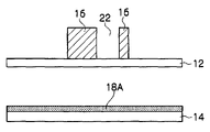
- the first cladding curable resin is applied in a layer form onto the second substrate (in the present exemplary embodiment, the upper cladding substrate 14 ), thereby forming a first cladding curable resin layer 18 A (see FIG. 4B ).
- the first cladding curable resin examples include ones similar to the cladding curable resin described later such as radiation curing resin, electron beam curing resin, and thermosetting resin.
- ultraviolet curing resin and thermosetting resin are preferable as the first curable resin.
- it is more preferable to select ultraviolet curing resin when deformation, peeling off and the like caused by expansion and shrinkage of the gas in the cavity 22 by the heat treatment are considered.
- the ultraviolet curing resin or the thermosetting resin an ultraviolet curing or thermosetting monomer or oligomer, or a mixture of a monomer and an oligomer may be used.
- epoxy, polyimide, or acrylic ultraviolet curing resin may be used.
- an ultraviolet lamp an ultraviolet LED, an ultraviolet radiation apparatus, or the like may be used.
- the material of the first cladding curable resin is preferably the same as that of the second curable resin for forming the second cladding 20 described later. It is to be noted that the material of the first cladding curable resin may be different from that of the second curable resin.
- the thickness of the first cladding curable resin layer 18 A is preferably not more than 15 ⁇ m, more preferably not more than 10 ⁇ m, and its lower limit is 5 ⁇ m. Although it depends on the viscosity, when the thickness of the first cladding curable resin is not less than a predetermined value, there are cases where the first cladding curable resin enters the cavity 22 when sealing the cavity 22 and because of this, the residual gas becomes bubbles and the reflecting surface is not flat; thus the object is not achieved. In addition, there are cases where yield decreases. For this reason, the thickness of the first cladding curable resin layer 18 A is preferably within the above-mentioned range.
- the first cladding curable resin layer 18 A be improved in viscosity, that is, have its fluidity suppressed after formed into a layer form.
- the method therefor include a method in which the first cladding curable resin layer 18 A is incompletely cured and a method in which the first cladding curable resin layer 18 A is cured so that the inside is cured with the surface uncured or incompletely cured.
- incompletely cured is a condition where the curing reaction is caused only partly, and means that the viscosity is higher than that of the first cladding curable resin in the unhardened state.
- the first cladding curable resin layer 18 A is cured so that the inside is cured with the surface uncureds or incompletely cured, fluidity is suppressed since only the inside of the first curable resin is cured to be solidified and only the surface is cured or incompletely cured.
- Curing the first cladding curable resin layer 18 A so that the inside is cured with the surface uncured or incompletely cured is realized by applying an ultraviolet curing radical polymer material (for example, acrylic resin) as the first cladding curable resin and curing the first cladding curable resin by ultraviolet rays in an atmosphere containing oxygen.
- the ultraviolet curing radical polymer material is difficult to harden because of oxygen inhibition.
- the sealing performance when the first cladding curable resin layer 18 A covers the opening of the cavity 22 is excellent and the entrance of the first cladding curable resin into the cavity 22 is suppressed. Consequently, the entrance of other foreign matter into the cavity 22 is also suppressed, so that an excellent reflecting surface can be maintained. Therefore, the optical waveguide has stable optical characteristics.
- first cladding curable resin layer 18 A may be formed over the entire area of the upper cladding substrate 14 having the same size as the lower cladding substrate 12 , it may be formed on the upper cladding substrate 14 that has a size corresponding only to a peripheral area of the cavity 22 (see FIGS. 6 to 8 ).
- the first cladding curable resin layer 18 A is provided only on the periphery of the area sealing the opening on the side of the upper cladding substrate 14 in the cavity 22 , for example, when the second curable resin is filled in the space surrounded by the lower cladding substrate 12 , the upper cladding substrate 14 and the waveguide core 16 by using a capillary action, suction or both of them, the distance is reduced, so that the time for filling the second curable resin is reduced.
- the method of applying the cladding to the remaining periphery of the core is not specifically limited. In doing this, the area may be further covered by a third substrate.
- the lower cladding substrate 12 and the upper cladding substrate 14 are disposed to face each other and the opening (in the present exemplary embodiment, the opening on the side of the upper cladding substrate 14 ) of the cavity 22 is sealed by the first cladding curable resin, thereby isolating the gas in the cavity 22 (see FIG. 4C ).
- This step is performed in an atmosphere of the residual gas in the cavity 22 while a predetermined pressure is applied between the lower cladding substrate 12 and the upper cladding substrate 14 , that is, while a predetermined pressure is applied to the surface of the waveguide core 16 .
- the first cladding curable resin is cured to form the first cladding 18 (see FIG. 4D ).
- This curing is performed, for example, by ultraviolet exposure when the first cladding curable resin is an ultraviolet curing type, and by heating when it is a thermosetting type.
- the resin is cured in an environment where oxygen is absent (for example, in a noble gas environment, or in a nitrogen environment).
- thermosetting type is used as the first cladding curable resin
- the first cladding curable resin is preferably hardened with the cavity 22 being vacuum.
- this method is not preferable because an expensive vacuum apparatus is required and the number of steps is increased.
- the second cladding curable resin is filled in the space surrounded by the lower cladding substrate 12 , the upper cladding substrate 14 , and the waveguide core 16 .
- the second cladding curable resin is filled, for example, from an opened end of the space by using a capillary action. In that case, the filling speed may be increased by performing decompression suction from the other opened end of the space.
- a resin such as radiation curing resin, electron beam curing resin, or thermosetting resin may be used.
- ultraviolet curing resin and thermosetting resin are preferably used. However, it is preferable to select ultraviolet curing resin when deformation, peeling off and the like caused by expansion and shrinkage of the gas trapped in the cavity 22 by the heat treatment are considered.
- an ultraviolet curing or thermosetting monomer or oligomer, or a mixture of a monomer and an oligomer is preferably used.
- epoxy, polyimide, or acrylic ultraviolet curing resin is preferably used.
- a polymer being miscible with the resin and not adversely affecting the refractive index, elasticity, and transmission characteristic of the resin may be added to the second cladding curable resin in order to reduce the volume change (shrinkage) after curing of the resin.
- the polymer is preferably added to the first cladding curable resin as well.
- the mold-forming curable resin in a combination using as the mold-forming curable resin a liquid silicone rubber, a liquid dimethylsiloxane rubber that becomes rubber when cured and using as the cladding substrates (upper and lower cladding substrates) alicyclic olefin resin having a norbornene structure in its main chain and having a polar group such as alkyloxycarbonyl group in its side chain, the adhesion between them is particular high, no deformation of the concave structure of the mold occurs, and the second cladding curable resin may be quickly filled into the concave portion by a capillary action even when the cross-sectional area of the concave structure is extremely small (for example, a rectangle of 10 ⁇ 10 ⁇ m).
- a lower viscosity for example, a viscosity (25° C.) of not less than 10 mPa ⁇ s and not more than 4000 mPa ⁇ s, preferably not less than 10 mPa ⁇ s and not more than 500 mPa ⁇ s
- a viscosity 25° C.
- the second cladding curable resin is cured to surround the waveguide core 16 , thereby forming the second cladding 20 having a lower refractive index than the waveguide core 16 (see FIG. 4E ).
- This curing is performed, for example, by ultraviolet exposure when the second cladding curable resin is an ultraviolet curing type, and by heating when it is a thermosetting type.
- ultraviolet curable resin for example, an ultraviolet lamp, an ultraviolet LED, or an ultraviolet radiation apparatus is used.
- thermosetting resin heating in an oven is used.
- the refractive index of the claddings (the second cladding 20 and the first cladding 18 ) be not more than 1.55, more preferably not more than 1.53.
- the difference in refractive index between the cladding substrate and the cladding is preferably small. It is preferable that the difference be within 0.05, more preferably within 0.001, and even more preferably 0 from the viewpoint of trapping light.
- both end surfaces in the direction of length of the optical waveguide are cut by a dicing saw or the like so as to be perpendicular or inclined with respect to the optical waveguide surface as required, thereby manufacturing the optical waveguide 10 .
- the method of cutting both end surfaces of the optical waveguide is not limited to the cutting method by a dicing saw.
- the number of through holes to fill or vacuum the waveguide core resin may be two or more.
- the branching also includes multistage branching.
- the through hole provided on the side of entrance of the core-forming curable resin has the function of storing liquid (core-forming curable resin).
- the through hole provided on the side of discharge of the core-forming curable resin is used for the decompression suction for decompressing the core-forming concave portion 24 A of the mold 24 when the resin is filled into the core-forming concave portion 24 A of the mold 24 .
- the configuration and size of the through hole on the entrance side is not specifically limited as long as the through hole communicates with the entrance end of the concave portion and has the liquid storing function.
- the configuration and size of the through hole on the discharge side is not specifically limited as long as the through hole communicates with the discharge end of the core-forming concave portion 24 A of the mold 24 and can be used for decompression suction.
- the through hole provided on the side of entrance of the core-forming curable resin of the core-forming concave portion 24 A of the mold 24 has the liquid storing function, by its cross section being large on the side in contact with the cladding substrate (lower cladding substrate 12 ) and decreasing with distance from the substrate when the mold 24 is in close contact with the substrate, the mold 24 and the lower cladding substrate 12 are easily separated from each other after the core-forming curable resin is filled in the core-forming concave portion 24 A of the mold 24 and cured. Since it is unnecessary for the through hole on the side of discharge of the core-forming curable resin to have the liquid storing function, it is not particularly necessary to adopt this cross-sectional structure to the through hole.
- a method is employed where a mold is formed in which the core-forming concave portion 24 A corresponding to the waveguide core 16 and the cavity-forming convex portion 24 B corresponding to the cavity 22 are formed as described above, and the through hole is formed by punching the mold in a predetermined shape. In doing this, the mold is punched so that the inlet for filling the core-forming curable resin and the outlet for discharging the core-forming curable resin from the concave portion appear inside the through hole.
- the through hole may be formed so that a part of the mold is left in the direction of thickness of the mold 24 as well as the type (punched type) in which the curing resin layer is all removed in the direction of thickness of the mold 24 as described above.
- the mold is placed below the lower cladding substrate 12 so that the through hole is exposed.
- the opening of the cavity 22 provided in the lower cladding substrate 12 is closed by the first cladding curable resin layer 18 A in a incompletely cured state where at least its surface is uncured, and then, the first cladding hardening resin layer 18 A is cured to form the first cladding. Thereafter, the second cladding curable resin is filled in the space surrounded by the upper cladding substrate 14 , the lower cladding substrate 12 and the waveguide core 16 , and is cured to form the second cladding 20 .
- the opening (the opening on the side of the upper cladding substrate 14 ) of the cavity 22 is sealed by the first cladding 18 with excellent adhesion when the second cladding curable resin is filled, so that the entrance of the second cladding curable resin into the cavity 22 is suppressed.
- the other opening (the opening on the side of the lower cladding substrate 12 ) of the cavity 22 is also formed with excellent adhesion by the lower cladding substrate 12 since the core-forming curable resin is applied and cured on the lower cladding substrate 12 to form the waveguide core 16 . Consequently, the entrance of the second cladding curable resin from the other opening is also suppressed. Consequently, the cavity 22 is present inside the waveguide core 16 with the entrance of foreign matter being suppressed. As a result, an optical waveguide is obtained in which it is suppressed that the optical characteristic becomes unstable.
- a polymer optical waveguide is formed that has the same structure as the optical waveguide shown in FIGS. 1 to 3 and has a 90-degree reflecting cavity in the waveguide core.
- a thick film resist is applied to Si substrate. Then, the substrate is prebaked at 80° C., and is exposed and developed through a photomask, thereby forming a core-forming convex portion (core width: 50 ⁇ m, core height: 50 ⁇ m) corresponding to the configuration of the core and a cavity-forming concave portion (depth: 50 ⁇ m) corresponding to the configuration of the cavity.
- the formed master is postbaked at 120° C. to complete the master.
- thermosetting dimethylsiloxane resin (SYLGARD 184 manufactured by Dow Corning Asia, Ltd.) is poured therein, left for a predetermined time, vacuum degassed for ten minutes, and heated at 120° C. for 30 minutes to be solidified. Then, the master is detached to form the mold having the cavity-forming convex portion and the core-forming concave portion. A hole with a diameter of 3 mm is formed in each of two positions on a line connecting the core-forming concave portions to form the filling hole and the suction hole.
- a film substrate (ARTON FILM manufactured by JSR Corp., refractive index: 1.51) with a thickness of 188 ⁇ m is prepared as the lower cladding substrate, and the mold is brought into close contact therewith.
- an ultraviolet curable resin with a viscosity of 800 mPa ⁇ s (refractive index after hardening: 1.54) is filled in the filling hole formed in the mold, and suction is performed through the suction hole by a suction pump, so that the ultraviolet curable resin is filled in the core-forming concave portion while the cavity remains.
- the resin is irradiated with an ultraviolet ray of 50 mW/cm 2 through the mold (dimethylsiloxane resin) for ten minutes to be cured. Thereafter, the mold is detached to form the waveguide core having a cavity opened at the top, on the lower cladding substrate.
- the upper cladding substrate where the first cladding curable resin layer is formed and the lower cladding substrate where the waveguide core and the cavity are formed are disposed so as to face each other and adhered to each other under a predetermined pressure, and the opening of the cavity is sealed by the first cladding curable resin layer to thereby trap gas (air) in the cavity.
- the first cladding hardening resin is cured to form the first cladding.
- an ultraviolet curable resin (refractive index after curing: 1.51, viscosity (25° C.): 360 mPa ⁇ s) is dropped to the end of the space and filled by using a capillary action. Thereafter, by applying an ultraviolet ray of 50 mW/cm 2 for ten minutes, the second cladding resin is cured to form the second cladding. When the inside of the cavity is observed, no entrance of the second cladding curable resin into the cavity is found.
- the end of the optical waveguide is cut out by using a dicing saw.
- an optical waveguide film is formed in which air is sealed in and a cavity serving as the reflecting surface is provided.
- a Gaussian beam with a wavelength of 850 nm emitted from a Fabry-Perot laser diode is made incident on the formed optical waveguide through an optical fiber, the light quantity is measured by a light intensity measuring instrument on the waveguide after reflection, and the reflection loss is calculated. The result of the calculation is 0.5 dB.
- the first cladding curable resin layer is formed on the upper cladding substrate, and is left for 90 minutes in room temperature environment.
- the cladding curable resin is incompletely cured and viscous.
- a Gaussian beam with a wavelength of 850 nm emitted from a Fabry-Perot laser diode is made incident on the formed optical waveguide through an optical fiber, the light quantity is measured by a light intensity measuring instrument at the end of the waveguide after reflection, and the reflection loss is calculated.
- the result of the calculation is 0.5 dB, which is equal to that of example 1.
Abstract
Description
θ=sin−1(n g /n c).
Claims (10)
Applications Claiming Priority (2)
| Application Number | Priority Date | Filing Date | Title |
|---|---|---|---|
| JP2007-075287 | 2007-03-22 | ||
| JP2007075287A JP4848986B2 (en) | 2007-03-22 | 2007-03-22 | Optical waveguide and method for manufacturing the same |
Publications (2)
| Publication Number | Publication Date |
|---|---|
| US20080232753A1 US20080232753A1 (en) | 2008-09-25 |
| US7542646B2 true US7542646B2 (en) | 2009-06-02 |
Family
ID=39774781
Family Applications (1)
| Application Number | Title | Priority Date | Filing Date |
|---|---|---|---|
| US12/033,039 Expired - Fee Related US7542646B2 (en) | 2007-03-22 | 2008-02-19 | Optical waveguide and method of manufacturing the same |
Country Status (2)
| Country | Link |
|---|---|
| US (1) | US7542646B2 (en) |
| JP (1) | JP4848986B2 (en) |
Families Citing this family (5)
| Publication number | Priority date | Publication date | Assignee | Title |
|---|---|---|---|---|
| JP5443494B2 (en) * | 2009-08-21 | 2014-03-19 | 株式会社東芝 | Optical element and display device |
| TW201213360A (en) * | 2010-04-06 | 2012-04-01 | Sumitomo Bakelite Co | An optical waveguide structure and an electronic device |
| US9711392B2 (en) * | 2012-07-25 | 2017-07-18 | Infineon Technologies Ag | Field emission devices and methods of making thereof |
| US9753217B2 (en) * | 2015-10-29 | 2017-09-05 | Xyratex Technology Limited | Stress relief for electro-optical printed circuit board |
| GB201721814D0 (en) * | 2017-12-22 | 2018-02-07 | Optoscribe Ltd | Optical apparatus, optical assembly and methods of manufacture thereof |
Citations (22)
| Publication number | Priority date | Publication date | Assignee | Title |
|---|---|---|---|---|
| JPH09145943A (en) | 1995-11-28 | 1997-06-06 | Mitsubishi Gas Chem Co Inc | Curved optical waveguide and its manufacture |
| JPH11248951A (en) | 1998-02-27 | 1999-09-17 | Hitachi Cable Ltd | Optical waveguide and its manufacture |
| US6259841B1 (en) | 1996-12-20 | 2001-07-10 | Corning Incorporated | Reflective coupling array for optical waveguide |
| JP2002333538A (en) | 2001-03-05 | 2002-11-22 | Fuji Xerox Co Ltd | Optical waveguide forming method, electrodeposition liquid used for it, and optical waveguide manufacturing apparatus |
| JP2003075670A (en) | 2001-08-31 | 2003-03-12 | Kddi Submarine Cable Systems Inc | Manufacturing method for reflector |
| JP2003207661A (en) | 2002-01-11 | 2003-07-25 | Omron Corp | Optical waveguide device |
| US20030179991A1 (en) | 2002-03-25 | 2003-09-25 | Fuji Photo Film Co., Ltd. | Optical deflection element |
| US6741781B2 (en) | 2000-09-29 | 2004-05-25 | Kabushiki Kaisha Toshiba | Optical interconnection circuit board and manufacturing method thereof |
| US6801701B1 (en) * | 2002-11-04 | 2004-10-05 | Litton Systems, Inc. | System for bending polymer or glass optical wave guides |
| US20040245660A1 (en) * | 2003-06-04 | 2004-12-09 | Fuji Xerox Co., Ltd. | Producing method of polymer optical waveguide |
| US20050175304A1 (en) | 2002-03-06 | 2005-08-11 | Marco Romagnoli | Method for guiding an electromagnetic radiation, in particular in an integrated optical device |
| US20050226562A1 (en) | 2002-03-06 | 2005-10-13 | Marco Romagnoli | Device for crossing optical beams, in particular in an integrated optical circuit |
| US6973248B2 (en) | 2002-08-19 | 2005-12-06 | Infineon Technologies Ag | Planar optical component, and a coupling device for coupling light between a planar optical component and an optical assembly |
| US6993213B2 (en) | 2002-11-21 | 2006-01-31 | Mitsubishi Denki Kabushiki Kaisha | Semiconductor optical waveguide device including s-shaped waveguides |
| US20060091571A1 (en) * | 2004-10-29 | 2006-05-04 | Fuji Xerox Co., Ltd. | Method for fabricating polymer optical waveguide device |
| US20060182399A1 (en) * | 2005-02-17 | 2006-08-17 | Chao-Kun Lin | System and method for low loss waveguide bends |
| US7164824B2 (en) * | 2004-12-10 | 2007-01-16 | Lucent Technologies Inc. | Waveguide turn for a waveguide circuit |
| US7206470B2 (en) * | 2003-10-24 | 2007-04-17 | University Of Alabama In Huntsville | Planar lightwave circuit waveguide bends and beamsplitters |
| US7242822B2 (en) * | 2003-12-26 | 2007-07-10 | International Business Machines Corporation | Optical connection board and optical signal transmission |
| US7308180B2 (en) * | 2005-06-02 | 2007-12-11 | Fuji Xerox Co., Ltd. | Optical waveguide and process for manufacturing the same |
| US20070292091A1 (en) * | 2006-06-19 | 2007-12-20 | Fuji Xerox Co., Ltd. | Optical waveguide, method of manufacturing the same and optical communication module |
| US7324723B2 (en) * | 2003-10-06 | 2008-01-29 | Mitsui Chemicals, Inc. | Optical waveguide having specular surface formed by laser beam machining |
Family Cites Families (2)
| Publication number | Priority date | Publication date | Assignee | Title |
|---|---|---|---|---|
| TW200628612A (en) * | 2000-07-19 | 2006-08-16 | Pharmacia & Up John Company | Substrates and assays for β-secretase activity |
| US20050226532A1 (en) * | 2004-04-01 | 2005-10-13 | Thompson Robert L | System and method for determining the size of an object |
-
2007
- 2007-03-22 JP JP2007075287A patent/JP4848986B2/en not_active Expired - Fee Related
-
2008
- 2008-02-19 US US12/033,039 patent/US7542646B2/en not_active Expired - Fee Related
Patent Citations (23)
| Publication number | Priority date | Publication date | Assignee | Title |
|---|---|---|---|---|
| US5872883A (en) | 1995-11-28 | 1999-02-16 | Mitsubishi Gas Chemical Company, Inc. | Curved optical waveguide and method of manufacturing the same |
| JPH09145943A (en) | 1995-11-28 | 1997-06-06 | Mitsubishi Gas Chem Co Inc | Curved optical waveguide and its manufacture |
| US6259841B1 (en) | 1996-12-20 | 2001-07-10 | Corning Incorporated | Reflective coupling array for optical waveguide |
| JPH11248951A (en) | 1998-02-27 | 1999-09-17 | Hitachi Cable Ltd | Optical waveguide and its manufacture |
| US6741781B2 (en) | 2000-09-29 | 2004-05-25 | Kabushiki Kaisha Toshiba | Optical interconnection circuit board and manufacturing method thereof |
| JP2002333538A (en) | 2001-03-05 | 2002-11-22 | Fuji Xerox Co Ltd | Optical waveguide forming method, electrodeposition liquid used for it, and optical waveguide manufacturing apparatus |
| JP2003075670A (en) | 2001-08-31 | 2003-03-12 | Kddi Submarine Cable Systems Inc | Manufacturing method for reflector |
| JP2003207661A (en) | 2002-01-11 | 2003-07-25 | Omron Corp | Optical waveguide device |
| US20050175304A1 (en) | 2002-03-06 | 2005-08-11 | Marco Romagnoli | Method for guiding an electromagnetic radiation, in particular in an integrated optical device |
| US20050226562A1 (en) | 2002-03-06 | 2005-10-13 | Marco Romagnoli | Device for crossing optical beams, in particular in an integrated optical circuit |
| US20030179991A1 (en) | 2002-03-25 | 2003-09-25 | Fuji Photo Film Co., Ltd. | Optical deflection element |
| US6973248B2 (en) | 2002-08-19 | 2005-12-06 | Infineon Technologies Ag | Planar optical component, and a coupling device for coupling light between a planar optical component and an optical assembly |
| US6801701B1 (en) * | 2002-11-04 | 2004-10-05 | Litton Systems, Inc. | System for bending polymer or glass optical wave guides |
| US6993213B2 (en) | 2002-11-21 | 2006-01-31 | Mitsubishi Denki Kabushiki Kaisha | Semiconductor optical waveguide device including s-shaped waveguides |
| US20040245660A1 (en) * | 2003-06-04 | 2004-12-09 | Fuji Xerox Co., Ltd. | Producing method of polymer optical waveguide |
| US7324723B2 (en) * | 2003-10-06 | 2008-01-29 | Mitsui Chemicals, Inc. | Optical waveguide having specular surface formed by laser beam machining |
| US7206470B2 (en) * | 2003-10-24 | 2007-04-17 | University Of Alabama In Huntsville | Planar lightwave circuit waveguide bends and beamsplitters |
| US7242822B2 (en) * | 2003-12-26 | 2007-07-10 | International Business Machines Corporation | Optical connection board and optical signal transmission |
| US20060091571A1 (en) * | 2004-10-29 | 2006-05-04 | Fuji Xerox Co., Ltd. | Method for fabricating polymer optical waveguide device |
| US7164824B2 (en) * | 2004-12-10 | 2007-01-16 | Lucent Technologies Inc. | Waveguide turn for a waveguide circuit |
| US20060182399A1 (en) * | 2005-02-17 | 2006-08-17 | Chao-Kun Lin | System and method for low loss waveguide bends |
| US7308180B2 (en) * | 2005-06-02 | 2007-12-11 | Fuji Xerox Co., Ltd. | Optical waveguide and process for manufacturing the same |
| US20070292091A1 (en) * | 2006-06-19 | 2007-12-20 | Fuji Xerox Co., Ltd. | Optical waveguide, method of manufacturing the same and optical communication module |
Also Published As
| Publication number | Publication date |
|---|---|
| JP2008233673A (en) | 2008-10-02 |
| JP4848986B2 (en) | 2011-12-28 |
| US20080232753A1 (en) | 2008-09-25 |
Similar Documents
| Publication | Publication Date | Title |
|---|---|---|
| US7308180B2 (en) | Optical waveguide and process for manufacturing the same | |
| US7539384B2 (en) | Optical waveguide and method of manufacturing the same | |
| US7248772B2 (en) | Flexible optical waveguide | |
| US7386213B2 (en) | Bidirectional communication optical waveguide and manufacturing method thereof | |
| JP2006017885A (en) | Waveguide film type optical module, optical waveguide film and its manufacturing method | |
| JP2006126568A (en) | Method for manufacturing polymer optical waveguide device | |
| US7604758B2 (en) | Process for producing polymer optical waveguide | |
| JP4144468B2 (en) | Multilayer polymer optical waveguide and method for manufacturing the same | |
| US7542646B2 (en) | Optical waveguide and method of manufacturing the same | |
| US7546010B2 (en) | Lens-incorporating optical waveguide, and method for manufacturing the same | |
| US20050158003A1 (en) | Method of producing polymer optical waveguide | |
| JP4581328B2 (en) | Polymer optical waveguide and optical element manufacturing method | |
| JP2009075288A (en) | Method of manufacturing polymer optical circuit | |
| JP2007086330A (en) | Method for manufacturing polymer optical waveguide device | |
| JP2007233303A (en) | Method of manufacturing polymer optical waveguide module | |
| JP2004184480A (en) | Manufacturing method of polymer optical waveguide | |
| JP4544083B2 (en) | Flexible optical waveguide | |
| JP4692405B2 (en) | Optical waveguide, method for manufacturing the same, and optical communication module | |
| JP2009288418A (en) | Optical waveguide | |
| JP2007047320A (en) | Optical waveguide for bidirectional communication and its manufacturing method | |
| JP2007041122A (en) | Method of manufacturing polymer optical waveguide, polymer optical waveguide, and optical module using the same | |
| JP4517704B2 (en) | Method for producing polymer optical waveguide | |
| JP4561059B2 (en) | Method for producing polymer optical waveguide | |
| JP4337559B2 (en) | Mold for producing polymer optical waveguide and method for producing polymer optical waveguide | |
| JP2007086223A (en) | Optical waveguide and method for manufacturing optical waveguide |
Legal Events
| Date | Code | Title | Description |
|---|---|---|---|
| AS | Assignment |
Owner name: FUJI XEROX CO., LTD., JAPAN Free format text: ASSIGNMENT OF ASSIGNORS INTEREST;ASSIGNORS:FUJII, AKIRA;SUZUKI, TOSHIHIKO;SHIMIZU, KEISHI;AND OTHERS;REEL/FRAME:020523/0172 Effective date: 20080208 |
|
| FEPP | Fee payment procedure |
Free format text: PAYOR NUMBER ASSIGNED (ORIGINAL EVENT CODE: ASPN); ENTITY STATUS OF PATENT OWNER: LARGE ENTITY |
|
| STCF | Information on status: patent grant |
Free format text: PATENTED CASE |
|
| FPAY | Fee payment |
Year of fee payment: 4 |
|
| FPAY | Fee payment |
Year of fee payment: 8 |
|
| FEPP | Fee payment procedure |
Free format text: MAINTENANCE FEE REMINDER MAILED (ORIGINAL EVENT CODE: REM.); ENTITY STATUS OF PATENT OWNER: LARGE ENTITY |
|
| LAPS | Lapse for failure to pay maintenance fees |
Free format text: PATENT EXPIRED FOR FAILURE TO PAY MAINTENANCE FEES (ORIGINAL EVENT CODE: EXP.); ENTITY STATUS OF PATENT OWNER: LARGE ENTITY |
|
| STCH | Information on status: patent discontinuation |
Free format text: PATENT EXPIRED DUE TO NONPAYMENT OF MAINTENANCE FEES UNDER 37 CFR 1.362 |
|
| FP | Lapsed due to failure to pay maintenance fee |
Effective date: 20210602 |