US7660377B2 - Device for estimating a timing correction loop error for a digital demodulator - Google Patents
Device for estimating a timing correction loop error for a digital demodulator Download PDFInfo
- Publication number
- US7660377B2 US7660377B2 US11/270,388 US27038805A US7660377B2 US 7660377 B2 US7660377 B2 US 7660377B2 US 27038805 A US27038805 A US 27038805A US 7660377 B2 US7660377 B2 US 7660377B2
- Authority
- US
- United States
- Prior art keywords
- digital
- digital signals
- providing
- signals
- complex
- Prior art date
- Legal status (The legal status is an assumption and is not a legal conclusion. Google has not performed a legal analysis and makes no representation as to the accuracy of the status listed.)
- Expired - Fee Related, expires
Links
Images


Classifications
-
- H—ELECTRICITY
- H04—ELECTRIC COMMUNICATION TECHNIQUE
- H04L—TRANSMISSION OF DIGITAL INFORMATION, e.g. TELEGRAPHIC COMMUNICATION
- H04L7/00—Arrangements for synchronising receiver with transmitter
- H04L7/0054—Detection of the synchronisation error by features other than the received signal transition
- H04L7/007—Detection of the synchronisation error by features other than the received signal transition detection of error based on maximum signal power, e.g. peak value, maximizing autocorrelation
-
- H—ELECTRICITY
- H04—ELECTRIC COMMUNICATION TECHNIQUE
- H04L—TRANSMISSION OF DIGITAL INFORMATION, e.g. TELEGRAPHIC COMMUNICATION
- H04L27/00—Modulated-carrier systems
- H04L27/0014—Carrier regulation
- H04L2027/0024—Carrier regulation at the receiver end
- H04L2027/0026—Correction of carrier offset
- H04L2027/003—Correction of carrier offset at baseband only
-
- H—ELECTRICITY
- H04—ELECTRIC COMMUNICATION TECHNIQUE
- H04L—TRANSMISSION OF DIGITAL INFORMATION, e.g. TELEGRAPHIC COMMUNICATION
- H04L27/00—Modulated-carrier systems
- H04L27/0014—Carrier regulation
- H04L2027/0044—Control loops for carrier regulation
- H04L2027/0053—Closed loops
- H04L2027/0057—Closed loops quadrature phase
-
- H—ELECTRICITY
- H04—ELECTRIC COMMUNICATION TECHNIQUE
- H04L—TRANSMISSION OF DIGITAL INFORMATION, e.g. TELEGRAPHIC COMMUNICATION
- H04L7/00—Arrangements for synchronising receiver with transmitter
- H04L7/0016—Arrangements for synchronising receiver with transmitter correction of synchronization errors
- H04L7/002—Arrangements for synchronising receiver with transmitter correction of synchronization errors correction by interpolation
- H04L7/0029—Arrangements for synchronising receiver with transmitter correction of synchronization errors correction by interpolation interpolation of received data signal
Definitions
- the present invention relates to a demodulator for digital transmission, in which symbols are transmitted by phase modulation, or by amplitude and phase modulation.
- each transmitted symbol is formed by one or several periods of a sinusoid, where one parameter among the amplitude, frequency and/or phase has been modified, the modified parameter being only able to take a limited number of discrete values.
- Equation (2) corresponds to the sum of two amplitude-modulated carriers in quadrature.
- phase ⁇ can take discrete values from among M values, which corresponds to M points or states in the complex plane.
- the arrangement of points in the complex plane is called a constellation.
- the number of bits that can be coded for each transmitted symbol is equal to Log 2 (M).
- FIG. 1 shows an example of a constellation for an ideal four-state phase modulation or QPSK (Quadrature Phase Shift Keying) modulation.
- QPSK Quadrature Phase Shift Keying
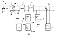
- FIG. 2 shows an example of a conventional demodulator 10 for phase-modulation digital transmission.
- Demodulator 10 receives a modulated signal v at an input terminal IN.
- Signal v is provided to a unit 12 (tuner) for transferring the signal in baseband.
- the operation of the baseband transfer unit requires determination of the frequency of the carrier used for the modulation of the transmitted symbols.
- Unit 12 provides two analog signals I*, Q* which correspond, in the complex plane of the constellation, to components of a complex signal s.
- Signals I*, Q* are converted into digital signals I* n , Q* n by analog-to-digital converters 14 (AD) controlled by a sampling clock signal CLK.
- AD analog-to-digital converters 14
- a carrier shift translates as a rotation of the constellation in the complex plane.
- a correction of the carrier shift is performed by a carrier shift correction loop 16 which comprises a correction unit 18 (corrector) which corrects signals I* n , Q* n and drives an adapted filter 20 which provides filtered digital signals I n , Q n .
- a carrier offset estimation unit 22 receives digital signals I n , Q n and determines an error signal representative of the carrier shift.
- the carrier shift error signal is transmitted to a filter 24 (carrier loop filter) which provides a control signal to correction unit 18 .
- phase modulation is not an ideal phase modulation.
- Such a correction concerns the determination of the sampling times of signals I* n , Q* n provided by unit 12 . Indeed, to limit the passband of the modulated signal, the carrier modulation is not performed by an abrupt switching from one state to another of the constellation but by a continuous transition between the constellation states. It is thus desirable for signals I*, Q* to be sampled at optimal times corresponding to the passing of signal s through states of the constellation and not at times corresponding to transitions between two states. Such a correction is performed by a timing correction loop 26 .
- Timing correction loop 26 comprises a timing error estimation device 28 which receives signals I n , Q n and provides an error signal Err n to a filter 30 (timing loop filter).
- Filter 30 provides a control signal Com to a voltage-controlled oscillator 32 (VCO) which provides sampling clock signal CLK to analog-to-digital converters 14 at a sampling frequency which depends on control signal Com.
- VCO voltage-controlled oscillator
- Timing error estimation devices There are several examples of timing error estimation devices.
- a first device example implements the Gardner algorithm (defined in the publication entitled “A BPSK/QPSK Timing Error Detector for Sampled Receivers”, IEEE Transactions of Communications, Vol. Com-34, pages 423-429, May 1986).
- n represents the index of the considered symbol.
- Such a determination of the error signal has the advantage of being independent from the phase of the carrier and thus accepts a significant carrier frequency shift.
- the provision of a usable error signal Err n thus does not require for the carrier shift correction loop 16 to have converged.
- a disadvantage of such a timing error estimation is that it requires determination, for a symbol of index n, of two additional inter-symbol values noted by indexes n ⁇ 1 ⁇ 2.
- Timing error estimation device uses the Mueller and Müller algorithm (defined in the publication entitled “Timing Recovery in Digital Synchronous Data Receivers”, IEEE Transactions on Communications, Vol. Com-26, pages 516-531, May 1976).
- the Mueller and Müller algorithm requires for an assumption to be made on the value of the complex signal corresponding to components I n , Q n , for example, considering that the constellation point closest to the sampled symbol corresponds to that which should be received.
- Such an error estimation has the advantage of not requiring determination of additional inter-symbol values between two sampled symbols.
- it has two significant disadvantages: the first one is that the constellation must be known, the second one is that it is sensitive to a shift of the carrier and thus requires for the carrier shift correction loop to have converged.
- the present invention aims at a timing error estimation device which requires no determination of additional inter-symbol values with respect to the sampled values and which is little sensitive to a carrier shift.
- the present invention aims at a timing error estimation device of simple design.
- the present invention provides a device for providing a digital error signal, for a timing correction loop of a digital demodulator for digital transmission by phase modulation or amplitude and phase modulation, the device successively receiving pairs of digital signals representative of the components of complex signals, and comprising means for providing a difference signal representative of the difference between the modulus, raised to a determined power, of the complex signal corresponding to the last received pair of digital signals and the modulus, raised to the determined power, of the complex signal corresponding to the previously-received pair of digital signals; means for providing a weighting factor which depends on the angle between the complex signal corresponding to the last received pair of digital signals and the complex signal corresponding to the previously-received pair of digital signals; and means for providing the error signal proportional to the product of the difference signal and of the weighting factor.
- the means for providing the weighting factor are capable of providing the weighting signal equal to the sum of a determined constant and of a term having its sign depending on the angle between the complex signal corresponding to the last received pair of digital signals and the complex signal corresponding to the previously-received pair of digital signals.
- the means for providing the weighting factor are capable of providing the weighting signal equal to the sum of the determined constant and of a term proportional to the cosine of the angle between the complex signal corresponding to the last received pair of digital signals and the complex signal corresponding to the previously-received pair of digital signals.
- the present invention also provides a timing correction loop for a digital demodulator for digital transmission in phase modulation or amplitude and phase modulation, comprising analog-to-digital converters receiving a pair of analog signals and successively providing, at the rate of a sampling clock signal, pairs of digital sampled signals representative of the components of complex signals; a device for providing a digital error signal such as previously defined, successively receiving pairs of digital signals obtained by filtering of the pairs of sampled digital signals; and means for providing a sampling clock signal having its frequency varying according to the error signal.
- the present invention also provides a timing correction loop for a digital demodulator for digital transmission in phase modulation or amplitude and phase modulation, comprising analog-to-digital converters receiving a pair of analog signals and successively providing at a determined frequency pairs of sampled digital signals representative of the components of complex signals; interpolation means receiving the sampled pairs of digital signals and capable of successively providing pairs of digital signals interpolated from last pairs of received sampled digital signals and on a control signal; a device for providing a digital error signal such as defined previously, successively receiving the pairs of interpolated digital signals; and means for providing the control signal which varies according to the error signal.
- the present invention also provides a digital demodulator receiving a signal modulated by a phase modulation or by an amplitude and phase modulation, comprising a unit of baseband transfer of the modulated signal capable of providing a pair of analog signals representative of the components of a complex signal; and a timing correction loop such as defined previously, receiving the pair of analog signals.
- the present invention also provides a method for providing a digital error signal, for a timing correction loop of a digital demodulator for digital transmission by phase modulation or by amplitude and phase modulation, comprising the steps of successively receiving pairs of digital signals representative of the components of complex signals; providing a difference signal representative of the difference between the modulus, raised to a determined power, of the complex signal corresponding to the last received pair of digital signals and the modulus, raised to the determined power, of the complex signal corresponding to the previously-received pair of digital signals; providing a weighting factor which depends on the angle between the complex signal corresponding to the last received pair of digital signals and the complex signal corresponding to the previously-received pair of digital signals; and providing the error signal proportional to the product of the difference signal and of the weighting factor.
- the weighting factor is equal to the sum of the determined constant and of a term proportional to the cosine of the angle between the complex signal corresponding to the last received pair of digital signals and the complex signal corresponding to the previously-received pair of digital signals.
- the weighting factor is equal to the sign of the sum of the determined constant and of a term equal to the cosine of the angle between the complex signal corresponding to the last received pair of digital signals and the complex signal corresponding to the previously-received pair of digital signals.
- the determined constant is zero.
- FIG. 1 shows an example of a constellation for a four-state phase modulation
- FIG. 2 schematically shows the main components of a demodulator for digital transmission by phase modulation
- FIG. 3 shows an example of the variation, in the constellation plane, of the analog complex signal obtained after baseband transfer of the modulated signal
- FIG. 4 shows an example of a time variation of the modulus of the analog complex signal obtained after baseband transfer of the modulated signal
- FIGS. 5 and 6 illustrate the timing error estimation method according to the present invention
- FIG. 7 shows in more detailed fashion the components of the filter used for the timing correction loop.
- FIG. 8 shows another example of the forming of the demodulator according to the present invention.
- the present invention provides an original structure of the timing error estimation device based on an analysis of the time variation of the complex analog signal s obtained from components I*, Q* provided by baseband transfer unit 12 .
- the present invention will now be described in the case of a four-state phase modulation (QPSK modulation). It should however be clear that the present invention also applies to any phase modulation. Further, as will be described in further detail hereafter, the present invention also applies to any modulation combining a phase modulation and an amplitude modulation.
- FIG. 3 shows an example of the variation in the complex plane of the constellation of complex analog signal s obtained from components I* and Q* provided by unit 12 in the case of a noiseless transmission.
- the black dots represent the different states of the constellation between which signal s varies.
- two states for which the angle, taken at the origin, between the two states is 180° are called opposite states. In the present invention, this will designate the states associated with bit sequence “00” and “11” and the states associated with bit sequence “10” and “01”.
- two states for which the angle, taken at the origin, between two states is 90° are called adjacent states. In the present example, this will designate the state couples associated with bit sequence “00” and “10”, “01” and “11”, “11” and “01”, and “01” and “00”.
- FIG. 4 shows an example of the variation of the modulus of s, noted ⁇ s ⁇ , in the time field. Since it is a phase modulation, ⁇ s ⁇ has the same value, noted S A , on passing through one of the states of the constellation. References t 1 to t 4 represent the times when s passes through one of the states of the constellation and thus correspond to the times at which a sampling must be performed by converters 14 . Generally, performing a filtering by adapted filter 20 requires the sampling frequency of converters 14 to be greater than the symbol frequency. The sampling frequency can then be a multiple of the symbol frequency. Only the filtered sample which has been determined at a time of passing through one of the constellation states is then kept for timing correction loop 26 .
- a transition between two opposite states corresponds to the transition between times t 2 and t 3 .
- ⁇ s ⁇ varies little, slightly decreasing or increasing with respect to S A .
- a transition between two adjacent states or between a state and the same state corresponds to the transitions between times t 1 and t 2 , and t 3 and t 4 .
- the present inventors have shown that, on transition between two states, the distribution of ⁇ s ⁇ is substantially symmetrical, in particular in the vicinity of the states.
- modules ⁇ S n ⁇ and ⁇ s n ⁇ 1 ⁇ may be obtained by approximate expressions.
- the first term in brackets substantially corresponds to the difference between the modulus of s sampled at time t n and the modulus of s sampled at the previous time t n ⁇ 1 . Given the substantially symmetrical variation of ⁇ s ⁇ between two optimal sampling states, the modulus difference is representative of the shift between the sampling times used with respect to the desired times.
- the first term in brackets of equation (7) is weighted by the second term in brackets, called the weighting factor.
- the weighting factor is equal to the sum of a constant and of a term proportional to the cosine of the angle, taken at the origin, between the two successive samples.
- FIGS. 5 and 6 illustrate the error signal determination method when signal s varies, respectively, from a state to the opposite state and from a state to the same state, or from a state to an adjacent state.
- the used sampling times t n ⁇ 1 and t n are ahead of optimal sampling times t* n ⁇ 1 and t* n , the shift between the used sampling times and the optimal sampling times being the same.
- Term ⁇ s n ⁇ s n ⁇ 1 ⁇ effectively appears, on transition from a state to an adjacent state or on transition from a state to the same state, to be much smaller than term ⁇ s n ⁇ s n ⁇ 1 ⁇ on transition between a state and the opposite state. More generally, for a phase modulation of more than four states, the transitions between a state and as remote as possible a state of the constellation provide the highest values for term ⁇ s n ⁇ s n ⁇ 1 ⁇ .
- the present inventors have shown that the contribution to error signal Err n is essentially due to term ⁇ s n ⁇ s n ⁇ 1 ⁇ .
- the transitions between a state and as remote as possible a state of the constellation providing the highest values for term ⁇ s n ⁇ s n ⁇ 1 ⁇ , such transitions are thus those taking the most part in the regulation performed by timing correction loop 26 . Since for such transitions, the variation of ⁇ s ⁇ is known with a strong probability, term ⁇ s n ⁇ s n ⁇ 1 ⁇ may thus be used to determine an error signal representative of the shift between the used sampling times and the optimal sampling times.
- the weighting factor introduces a non-linearity in the expression of error signal Err n which ensures a convergence of timing correction loop 26 .
- timing correction loop 26 also converges for a modulation combining an amplitude modulation and a phase modulation.
- the weighting factor may, besides, enable further limiting the participation in the regulation obtained by the timing correction loop of the transitions between a state and the same state or between a state and the adjacent state.
- the weighting factor is zero for a transition between a state and an adjacent state since the angle between s n and s n ⁇ 1 then is approximately 90°.
- the weighting factor is approximately 1 ⁇ 2 for a transition between a state and the same state and approximately ⁇ 1 ⁇ 2 for a transition between a state and an adjacent state.
- the weighting factor may be selected to privilege, for the determination of error signal Err n , the transitions between two states for which the angle between states is closest to 180° or 0° with respect to the transitions between two states for which the angle between states is closest to 0° or to 90°.
- the weighting factor may be replaced with the sign of the second term in brackets of equation (7). Timing correction loop 26 thus always enables obtaining the convergence of the sampling times towards the optimal sampling times.
- modulus ⁇ s n ⁇ may be replaced with an approximate expression.
- the first term in brackets of equation (7) may be replaced with the difference of the squares of the modules of the successive samples of s.
- error estimation unit 28 is obtained with dedicated circuits, the determination of the square of the modulus of a complex signal may, in general, be obtained more simply than the simple determination of the modulus.
- FIG. 7 shows an example of the forming of filter 30 of timing correction loop 26 .
- Filter 30 comprises two paths: a proportional path and an integral path.
- error signal Err n is provided to an amplification unit 32 in which it is multiplied by a proportionality constant Kp, then provided to a first input of an adder 34 .
- signal Err n is provided to an amplifier 34 in which it is multiplied by an integration constant K i , then provided to a first input of an adder 36 .
- the output of adder 36 drives a shift unit 38 which stores, on each symbol clock pulse, the value provided by adder 36 and provides the value previously stored to the second input of adder 36 .
- the output of shift unit 38 is provided to the second input of adder 34 .
- Adder 34 provides control signal Com.
- Such a first order filter conventionally enables following a sampling error both in phase and frequency.
- FIG. 8 illustrates another example of a demodulator 40 for digital transmission by phase modulation in which timing error estimation unit 28 according to the present invention may be used.
- Elements common with demodulator 10 shown in FIG. 2 are indicated with same reference numerals.
- analog-to-digital converters 14 sample at a fixed sampling frequency the signals I* and Q* provided by the baseband transfer unit and drive an interpolator 42 , capable of determining, by an interpolation algorithm, at least one sample per symbol based on the successive samples provided by each converter 14 at a determined time and on control signal Com.
- the rest of demodulator 30 is identical to demodulator 10 shown in FIG. 2 , where the carrier shift correction loop is not shown.
- the error signal provided by the timing error estimation unit according to the present invention is independent from the carrier shift. Indeed, since the first term in brackets of equation (7) is formed by the difference between two modules, it is independent from any rotation of the constellation which results from an incorrect transposition of the baseband-modulated signal. The second term in brackets of equation (7) being proportional to the cosine of the angle of two successive samples, it is also independent from any rotation of the constellation, if said rotation is sufficiently slow, which is generally the case at this step of the demodulation.
- the timing error estimation unit does not require determination of additional inter-symbol values between two samples. This enables simplifying the structure of the timing error estimation unit when it is formed by dedicated circuits.
- the algorithm implemented for the error signal determination is relatively simple. This enables simplifying the structure of the timing error estimation unit when it is formed by dedicated circuits.
- the carrier shift correction loop has been shown as interleaved with the timing correction loop.
- the carrier shift correction loop may however be provided before or after the timing correction loop.
Abstract
Description
v(t)=A cos(2πft+φ(t)) (1)
v(t)=A[cos 2πft*cos φ(t)−sin πft*sin φ(t)] (2)
v(t)=Re(ae j(2πft+φ))=Re(ae jφ e j2πft) (3)
I=a×cos φ and Q=a×sin φ (4)
v(t)=x cos 2πft+y sin 2πft (5)
Err n =I n [I n+1/2 −I n−1/2 ]+Q n [Q n+1/2 −Q n−1/2] (6)
Err n =[∥s n ∥−∥s n−1 ∥]·[Re(s n ·s* n−1 −A)] (7)
∥s n ∥=∥I n +jQ n ∥≈sup(|I n| ,|Q n|)+½inf(|I n| ,|Q n|) (8)
Claims (10)
Applications Claiming Priority (3)
| Application Number | Priority Date | Filing Date | Title |
|---|---|---|---|
| FR0452576A FR2877787A1 (en) | 2004-11-09 | 2004-11-09 | CADENCE CORRECTION LOOP ERROR ESTIMATING DEVICE FOR DIGITAL DEMODULATOR |
| FR0452576 | 2004-11-09 | ||
| FR04/52576 | 2004-11-09 |
Publications (2)
| Publication Number | Publication Date |
|---|---|
| US20060098763A1 US20060098763A1 (en) | 2006-05-11 |
| US7660377B2 true US7660377B2 (en) | 2010-02-09 |
Family
ID=34951603
Family Applications (1)
| Application Number | Title | Priority Date | Filing Date |
|---|---|---|---|
| US11/270,388 Expired - Fee Related US7660377B2 (en) | 2004-11-09 | 2005-11-09 | Device for estimating a timing correction loop error for a digital demodulator |
Country Status (3)
| Country | Link |
|---|---|
| US (1) | US7660377B2 (en) |
| EP (1) | EP1655882A1 (en) |
| FR (1) | FR2877787A1 (en) |
Cited By (2)
| Publication number | Priority date | Publication date | Assignee | Title |
|---|---|---|---|---|
| US9197262B2 (en) | 2006-09-29 | 2015-11-24 | Broadcom Corporation | Low-power and low-cost adaptive self-linearization system with fast convergence |
| EP3579458A1 (en) | 2018-06-06 | 2019-12-11 | Newtec Cy | System for synchronizing a ground segment to a beam hopping satellite |
Families Citing this family (4)
| Publication number | Priority date | Publication date | Assignee | Title |
|---|---|---|---|---|
| US8041757B2 (en) | 2006-09-29 | 2011-10-18 | Netlogic Microsystems, Inc. | Low power and low complexity adaptive self-linearization |
| US7602321B2 (en) * | 2006-09-29 | 2009-10-13 | Optichron, Inc. | Adaptive composite analog to digital converter |
| US8032336B2 (en) * | 2006-09-29 | 2011-10-04 | Netlogic Microsystems, Inc. | Distortion cancellation using adaptive linearization |
| EP1956701B1 (en) * | 2007-02-08 | 2012-03-28 | Infineon Technologies Austria AG | DC/DC-converter with a band pass filter and a band rejection filter in the voltage control loop |
Citations (7)
| Publication number | Priority date | Publication date | Assignee | Title |
|---|---|---|---|---|
| US4416015A (en) | 1981-12-30 | 1983-11-15 | Bell Telephone Laboratories, Incorporated | Timing acquisition in voiceband data sets |
| US4646173A (en) * | 1984-06-20 | 1987-02-24 | Robert Bosch Gmbh | Converting and decoding receiver for digital data recorded in analog form on magnetic tape |
| US20010017902A1 (en) | 2000-01-31 | 2001-08-30 | Taku Yamagata | Timing error detection circuit, demodulation circuit and methods thereof |
| US20010031021A1 (en) | 2000-03-17 | 2001-10-18 | Mitsubishi Denki Kabushiki Kaisha, 2-3, Marunouchi 2-Chome, Chiyoda-Ku, Tokyo, Japan | Method and apparatus for reproducing timing, and a demodulating apparatus that uses the method and apparatus for reproducing timing |
| US20010048723A1 (en) | 2000-05-04 | 2001-12-06 | Oh Ji-Sung | VSB/QAM receiver and method |
| US6377634B1 (en) * | 1997-12-15 | 2002-04-23 | Nec Corporation | Circuit for reproducing bit timing and method of reproducing bit timing |
| US6621857B1 (en) | 1999-12-31 | 2003-09-16 | Thomson Licensing S.A. | Carrier tracking loop for direct sequence spread spectrum systems |
-
2004
- 2004-11-09 FR FR0452576A patent/FR2877787A1/en not_active Withdrawn
-
2005
- 2005-11-08 EP EP05110491A patent/EP1655882A1/en not_active Withdrawn
- 2005-11-09 US US11/270,388 patent/US7660377B2/en not_active Expired - Fee Related
Patent Citations (7)
| Publication number | Priority date | Publication date | Assignee | Title |
|---|---|---|---|---|
| US4416015A (en) | 1981-12-30 | 1983-11-15 | Bell Telephone Laboratories, Incorporated | Timing acquisition in voiceband data sets |
| US4646173A (en) * | 1984-06-20 | 1987-02-24 | Robert Bosch Gmbh | Converting and decoding receiver for digital data recorded in analog form on magnetic tape |
| US6377634B1 (en) * | 1997-12-15 | 2002-04-23 | Nec Corporation | Circuit for reproducing bit timing and method of reproducing bit timing |
| US6621857B1 (en) | 1999-12-31 | 2003-09-16 | Thomson Licensing S.A. | Carrier tracking loop for direct sequence spread spectrum systems |
| US20010017902A1 (en) | 2000-01-31 | 2001-08-30 | Taku Yamagata | Timing error detection circuit, demodulation circuit and methods thereof |
| US20010031021A1 (en) | 2000-03-17 | 2001-10-18 | Mitsubishi Denki Kabushiki Kaisha, 2-3, Marunouchi 2-Chome, Chiyoda-Ku, Tokyo, Japan | Method and apparatus for reproducing timing, and a demodulating apparatus that uses the method and apparatus for reproducing timing |
| US20010048723A1 (en) | 2000-05-04 | 2001-12-06 | Oh Ji-Sung | VSB/QAM receiver and method |
Non-Patent Citations (1)
| Title |
|---|
| French Search Report from French Patent Application 04/52576, filed Nov. 9, 2004. |
Cited By (5)
| Publication number | Priority date | Publication date | Assignee | Title |
|---|---|---|---|---|
| US9197262B2 (en) | 2006-09-29 | 2015-11-24 | Broadcom Corporation | Low-power and low-cost adaptive self-linearization system with fast convergence |
| EP3579458A1 (en) | 2018-06-06 | 2019-12-11 | Newtec Cy | System for synchronizing a ground segment to a beam hopping satellite |
| WO2019233684A1 (en) | 2018-06-06 | 2019-12-12 | Newtec Cy | System for synchronizing a ground segment to a beam hopping satellite |
| EP3761524A1 (en) | 2018-06-06 | 2021-01-06 | ST Engineering iDirect (Europe) Cy NV | System for synchronizing a ground segment to a beam hopping satellite |
| US11381305B2 (en) | 2018-06-06 | 2022-07-05 | St Engineering Idirect (Europe) Cy Nv | System for synchronizing a ground segment to a beam hopping satellite |
Also Published As
| Publication number | Publication date |
|---|---|
| FR2877787A1 (en) | 2006-05-12 |
| EP1655882A1 (en) | 2006-05-10 |
| US20060098763A1 (en) | 2006-05-11 |
Similar Documents
| Publication | Publication Date | Title |
|---|---|---|
| CA2170344C (en) | Signal processing system | |
| Mengali | Synchronization techniques for digital receivers | |
| US5093847A (en) | Adaptive phase lock loop | |
| US6606010B1 (en) | Quadrature vestigial sideband digital communications method | |
| US6236687B1 (en) | Decision directed phase locked loop (DD-PLL) for use with short block codes in digital communication systems | |
| EP0989707B1 (en) | Phase estimation in carrier recovery for QAM signals | |
| US7660377B2 (en) | Device for estimating a timing correction loop error for a digital demodulator | |
| US20110097092A1 (en) | Optical Receiver Having Fractional Sampling | |
| CN111343125B (en) | 32APSK modulation system receiver synchronization method | |
| CN101005480B (en) | Demodulation circuit and demodulation method | |
| WO2014194940A1 (en) | Coherent optical receiver | |
| US4528512A (en) | Timing synchronizing circuit for demodulators | |
| US6996191B1 (en) | Efficient accurate controller for envelope feedforward power amplifiers | |
| US5914985A (en) | Digital demodulator | |
| WO2007043124A9 (en) | Oversampling transversal equalizer | |
| US5640125A (en) | Digital PSK-type demodulator having clock recovery before carrier recovery | |
| KR100466589B1 (en) | Apparatus and method for digital symbol synchronization | |
| JP4438581B2 (en) | Demodulator and demodulation method | |
| KR100326263B1 (en) | Quadrature Amplitude Modulation Demodulator for symbol timing recovery with low noise and high speed | |
| JP4101777B2 (en) | Timing synchronization circuit | |
| JP4335125B2 (en) | Timing synchronization circuit | |
| CN114785475B (en) | Enhancement method for Gardner timing error detection | |
| KR100354839B1 (en) | Device for recovering symbol timing and for small area and low noise | |
| JP5168111B2 (en) | Demodulator having phase uncertainty elimination function and carrier slip compensation method thereof | |
| CA2330645A1 (en) | An apparatus and method for demodulating signals |
Legal Events
| Date | Code | Title | Description |
|---|---|---|---|
| AS | Assignment |
Owner name: STMICROELECTRONICS S.A.,FRANCE Free format text: ASSIGNMENT OF ASSIGNORS INTEREST;ASSIGNOR:MEYER, JACQUES;REEL/FRAME:017221/0782 Effective date: 20051010 Owner name: STMICROELECTRONICS S.A., FRANCE Free format text: ASSIGNMENT OF ASSIGNORS INTEREST;ASSIGNOR:MEYER, JACQUES;REEL/FRAME:017221/0782 Effective date: 20051010 |
|
| STCF | Information on status: patent grant |
Free format text: PATENTED CASE |
|
| CC | Certificate of correction | ||
| FPAY | Fee payment |
Year of fee payment: 4 |
|
| FPAY | Fee payment |
Year of fee payment: 8 |
|
| FEPP | Fee payment procedure |
Free format text: MAINTENANCE FEE REMINDER MAILED (ORIGINAL EVENT CODE: REM.); ENTITY STATUS OF PATENT OWNER: LARGE ENTITY |
|
| LAPS | Lapse for failure to pay maintenance fees |
Free format text: PATENT EXPIRED FOR FAILURE TO PAY MAINTENANCE FEES (ORIGINAL EVENT CODE: EXP.); ENTITY STATUS OF PATENT OWNER: LARGE ENTITY |
|
| STCH | Information on status: patent discontinuation |
Free format text: PATENT EXPIRED DUE TO NONPAYMENT OF MAINTENANCE FEES UNDER 37 CFR 1.362 |
|
| FP | Lapsed due to failure to pay maintenance fee |
Effective date: 20220209 |