US7691734B2 - Deep trench based far subcollector reachthrough - Google Patents
Deep trench based far subcollector reachthrough Download PDFInfo
- Publication number
- US7691734B2 US7691734B2 US11/680,637 US68063707A US7691734B2 US 7691734 B2 US7691734 B2 US 7691734B2 US 68063707 A US68063707 A US 68063707A US 7691734 B2 US7691734 B2 US 7691734B2
- Authority
- US
- United States
- Prior art keywords
- doped
- deep trench
- dopants
- subcollector
- region
- Prior art date
- Legal status (The legal status is an assumption and is not a legal conclusion. Google has not performed a legal analysis and makes no representation as to the accuracy of the status listed.)
- Expired - Fee Related, expires
Links
- 239000004065 semiconductor Substances 0.000 claims abstract description 122
- 239000000463 material Substances 0.000 claims abstract description 83
- 239000002019 doping agent Substances 0.000 claims abstract description 64
- 239000000758 substrate Substances 0.000 claims abstract description 61
- 238000005468 ion implantation Methods 0.000 claims abstract description 20
- 229910052751 metal Inorganic materials 0.000 claims abstract description 20
- 239000002184 metal Substances 0.000 claims abstract description 20
- 238000000034 method Methods 0.000 claims description 22
- 238000004519 manufacturing process Methods 0.000 claims description 7
- 238000000151 deposition Methods 0.000 claims description 5
- 238000005530 etching Methods 0.000 claims description 4
- 238000000059 patterning Methods 0.000 claims description 4
- 229920002120 photoresistant polymer Polymers 0.000 description 15
- 150000002500 ions Chemical class 0.000 description 13
- 238000002955 isolation Methods 0.000 description 12
- 229910045601 alloy Inorganic materials 0.000 description 11
- 239000000956 alloy Substances 0.000 description 11
- 229910021417 amorphous silicon Inorganic materials 0.000 description 10
- 239000005388 borosilicate glass Substances 0.000 description 10
- 239000005360 phosphosilicate glass Substances 0.000 description 10
- 229910021420 polycrystalline silicon Inorganic materials 0.000 description 10
- 229910052581 Si3N4 Inorganic materials 0.000 description 7
- HQVNEWCFYHHQES-UHFFFAOYSA-N silicon nitride Chemical compound N12[Si]34N5[Si]62N3[Si]51N64 HQVNEWCFYHHQES-UHFFFAOYSA-N 0.000 description 7
- VYPSYNLAJGMNEJ-UHFFFAOYSA-N Silicium dioxide Chemical compound O=[Si]=O VYPSYNLAJGMNEJ-UHFFFAOYSA-N 0.000 description 6
- XUIMIQQOPSSXEZ-UHFFFAOYSA-N Silicon Chemical compound [Si] XUIMIQQOPSSXEZ-UHFFFAOYSA-N 0.000 description 6
- 229910052710 silicon Inorganic materials 0.000 description 6
- 239000010703 silicon Substances 0.000 description 6
- 229910052814 silicon oxide Inorganic materials 0.000 description 6
- 239000011521 glass Substances 0.000 description 5
- 229920005591 polysilicon Polymers 0.000 description 5
- 238000005452 bending Methods 0.000 description 4
- 230000015572 biosynthetic process Effects 0.000 description 4
- 239000012212 insulator Substances 0.000 description 4
- KRHYYFGTRYWZRS-UHFFFAOYSA-N Fluorane Chemical compound F KRHYYFGTRYWZRS-UHFFFAOYSA-N 0.000 description 3
- -1 boron ions Chemical class 0.000 description 3
- 150000001875 compounds Chemical class 0.000 description 3
- 238000009792 diffusion process Methods 0.000 description 3
- 230000001590 oxidative effect Effects 0.000 description 3
- 230000008901 benefit Effects 0.000 description 2
- 238000005229 chemical vapour deposition Methods 0.000 description 2
- 239000004020 conductor Substances 0.000 description 2
- 238000007796 conventional method Methods 0.000 description 2
- 230000008021 deposition Effects 0.000 description 2
- 238000000407 epitaxy Methods 0.000 description 2
- 238000002513 implantation Methods 0.000 description 2
- 238000001459 lithography Methods 0.000 description 2
- 238000012986 modification Methods 0.000 description 2
- 230000004048 modification Effects 0.000 description 2
- 229910021332 silicide Inorganic materials 0.000 description 2
- FVBUAEGBCNSCDD-UHFFFAOYSA-N silicide(4-) Chemical compound [Si-4] FVBUAEGBCNSCDD-UHFFFAOYSA-N 0.000 description 2
- 239000000126 substance Substances 0.000 description 2
- JBRZTFJDHDCESZ-UHFFFAOYSA-N AsGa Chemical compound [As]#[Ga] JBRZTFJDHDCESZ-UHFFFAOYSA-N 0.000 description 1
- 229910001339 C alloy Inorganic materials 0.000 description 1
- 229910001218 Gallium arsenide Inorganic materials 0.000 description 1
- 229910000673 Indium arsenide Inorganic materials 0.000 description 1
- GPXJNWSHGFTCBW-UHFFFAOYSA-N Indium phosphide Chemical compound [In]#P GPXJNWSHGFTCBW-UHFFFAOYSA-N 0.000 description 1
- 229910000577 Silicon-germanium Inorganic materials 0.000 description 1
- AXQKVSDUCKWEKE-UHFFFAOYSA-N [C].[Ge].[Si] Chemical compound [C].[Ge].[Si] AXQKVSDUCKWEKE-UHFFFAOYSA-N 0.000 description 1
- LEVVHYCKPQWKOP-UHFFFAOYSA-N [Si].[Ge] Chemical compound [Si].[Ge] LEVVHYCKPQWKOP-UHFFFAOYSA-N 0.000 description 1
- 229910052785 arsenic Inorganic materials 0.000 description 1
- 229910052796 boron Inorganic materials 0.000 description 1
- 230000015556 catabolic process Effects 0.000 description 1
- 230000007547 defect Effects 0.000 description 1
- 239000003989 dielectric material Substances 0.000 description 1
- 230000005611 electricity Effects 0.000 description 1
- 229910052732 germanium Inorganic materials 0.000 description 1
- GNPVGFCGXDBREM-UHFFFAOYSA-N germanium atom Chemical compound [Ge] GNPVGFCGXDBREM-UHFFFAOYSA-N 0.000 description 1
- 239000007943 implant Substances 0.000 description 1
- RPQDHPTXJYYUPQ-UHFFFAOYSA-N indium arsenide Chemical compound [In]#[As] RPQDHPTXJYYUPQ-UHFFFAOYSA-N 0.000 description 1
- QPJSUIGXIBEQAC-UHFFFAOYSA-N n-(2,4-dichloro-5-propan-2-yloxyphenyl)acetamide Chemical compound CC(C)OC1=CC(NC(C)=O)=C(Cl)C=C1Cl QPJSUIGXIBEQAC-UHFFFAOYSA-N 0.000 description 1
- 229910052698 phosphorus Inorganic materials 0.000 description 1
- 239000011574 phosphorus Substances 0.000 description 1
- 229910021483 silicon-carbon alloy Inorganic materials 0.000 description 1
Images


Classifications
-
- H—ELECTRICITY
- H01—ELECTRIC ELEMENTS
- H01L—SEMICONDUCTOR DEVICES NOT COVERED BY CLASS H10
- H01L21/00—Processes or apparatus adapted for the manufacture or treatment of semiconductor or solid state devices or of parts thereof
- H01L21/70—Manufacture or treatment of devices consisting of a plurality of solid state components formed in or on a common substrate or of parts thereof; Manufacture of integrated circuit devices or of parts thereof
- H01L21/71—Manufacture of specific parts of devices defined in group H01L21/70
- H01L21/76—Making of isolation regions between components
- H01L21/763—Polycrystalline semiconductor regions
-
- H—ELECTRICITY
- H01—ELECTRIC ELEMENTS
- H01L—SEMICONDUCTOR DEVICES NOT COVERED BY CLASS H10
- H01L29/00—Semiconductor devices adapted for rectifying, amplifying, oscillating or switching, or capacitors or resistors with at least one potential-jump barrier or surface barrier, e.g. PN junction depletion layer or carrier concentration layer; Details of semiconductor bodies or of electrodes thereof ; Multistep manufacturing processes therefor
- H01L29/02—Semiconductor bodies ; Multistep manufacturing processes therefor
- H01L29/06—Semiconductor bodies ; Multistep manufacturing processes therefor characterised by their shape; characterised by the shapes, relative sizes, or dispositions of the semiconductor regions ; characterised by the concentration or distribution of impurities within semiconductor regions
- H01L29/08—Semiconductor bodies ; Multistep manufacturing processes therefor characterised by their shape; characterised by the shapes, relative sizes, or dispositions of the semiconductor regions ; characterised by the concentration or distribution of impurities within semiconductor regions with semiconductor regions connected to an electrode carrying current to be rectified, amplified or switched and such electrode being part of a semiconductor device which comprises three or more electrodes
- H01L29/0821—Collector regions of bipolar transistors
-
- H—ELECTRICITY
- H01—ELECTRIC ELEMENTS
- H01L—SEMICONDUCTOR DEVICES NOT COVERED BY CLASS H10
- H01L29/00—Semiconductor devices adapted for rectifying, amplifying, oscillating or switching, or capacitors or resistors with at least one potential-jump barrier or surface barrier, e.g. PN junction depletion layer or carrier concentration layer; Details of semiconductor bodies or of electrodes thereof ; Multistep manufacturing processes therefor
- H01L29/66—Types of semiconductor device ; Multistep manufacturing processes therefor
- H01L29/66007—Multistep manufacturing processes
- H01L29/66075—Multistep manufacturing processes of devices having semiconductor bodies comprising group 14 or group 13/15 materials
- H01L29/66227—Multistep manufacturing processes of devices having semiconductor bodies comprising group 14 or group 13/15 materials the devices being controllable only by the electric current supplied or the electric potential applied, to an electrode which does not carry the current to be rectified, amplified or switched, e.g. three-terminal devices
- H01L29/66234—Bipolar junction transistors [BJT]
- H01L29/66272—Silicon vertical transistors
-
- H—ELECTRICITY
- H01—ELECTRIC ELEMENTS
- H01L—SEMICONDUCTOR DEVICES NOT COVERED BY CLASS H10
- H01L29/00—Semiconductor devices adapted for rectifying, amplifying, oscillating or switching, or capacitors or resistors with at least one potential-jump barrier or surface barrier, e.g. PN junction depletion layer or carrier concentration layer; Details of semiconductor bodies or of electrodes thereof ; Multistep manufacturing processes therefor
- H01L29/66—Types of semiconductor device ; Multistep manufacturing processes therefor
- H01L29/68—Types of semiconductor device ; Multistep manufacturing processes therefor controllable by only the electric current supplied, or only the electric potential applied, to an electrode which does not carry the current to be rectified, amplified or switched
- H01L29/70—Bipolar devices
- H01L29/72—Transistor-type devices, i.e. able to continuously respond to applied control signals
- H01L29/73—Bipolar junction transistors
- H01L29/732—Vertical transistors
Definitions
- the present invention relates to semiconductor structures, and particularly to semiconductor structures with a far subcollector and a deep trench based far subcollector reachthrough and methods of manufacturing the same.
- Some high performance passive semiconductor devices benefit from increased depth of a buried doped layer within a semiconductor substrate.
- an increase in the subcollector depth in a bipolar transistor offers the advantage of an increased breakdown voltage.
- the operating frequency of a positive-intrinsic-negative (PIN) diode in which an intrinsic semiconductor area is sandwiched between a p-doped semiconductor area and an n-doped area, increases with the depth of a buried doped layer, which functions as one terminal of the PIN diode.
- the depth of a buried doped layer is typically limited by the ability to form a reachthrough to the buried doped layer.
- a deep buried doped layer may be formed by implanting a semiconductor region followed by an epitaxy of semiconductor material of significant thickness, for example, greater than 2 microns
- the depth of the reachthrough that can be formed by ion implantation is limited by the projected range of the implanted ions.
- the projected range of boron ions in silicon accelerated at 1.0 MeV is only about 1.8 microns.
- the projected ranges for phosphorus ions and arsenic ions accelerated at 1.0 MeV are even less, and are only about 1.2 microns and 0.6 microns, respectively.
- the buried doped layers often require heavy doping concentrations on the order of 5.0 ⁇ 10 20 /cm 3 to achieve low resistivity. Implantation of dopants at such high energy and at such a high dose requires a long implantation time on a high performance ion implanter, and consequently, high processing costs. Further, even if such processing steps are employed, the depth of a buried doped layer does not exceed 2.0 microns unless the ion implantation energy is increased even higher, which is difficult to achieve with commercially available ion implanters.
- a method of forming a buried doped layer, or a “far subcollector”, at a depth greater than the projected range implanted ions by employing multiple stages of reachthroughs is known in the prior art.
- a doped region is formed on an initial semiconductor substrate.
- a first epitaxial semiconductor layer is grown on the surface of the initial semiconductor substrate up to a thickness through which a reachthrough may be formed by ion implantation, that is, up to the thickness of the projected range of ions of the subsequent ion implantation process.
- a second epitaxial semiconductor layer is grown on the first epitaxially grown layer.
- a second reachthrough is formed by ion implantation into the second epitaxially grown layer.
- each round of epitaxial growth of a semiconductor layer extends the depth of a buried semiconductor layer by the projected range of the subsequent ion implantation, that is, by the depth of the reachthrough subsequently formed therein.
- the increase in the depth of the buried doped layer is practically limited to less than about 1.2 ⁇ 1.8 microns due to the energy limitations on the available ion implanters.
- high temperature requirement for epitaxy of a semiconductor material causes bulk diffusion of the dopants in the buried doped layer, thereby reducing the depth of the buried doped layer and also reducing the doping density, and consequently, the conductivity of the buried doped layer.
- the present invention addresses the needs described above by providing a semiconductor structure with a far subcollector contacting a reachthrough region that is formed on and outside a wall of at least one deep trench and methods of manufacturing the same.
- the present invention forms a far subcollector on a surface of an initial semiconductor substrate, followed by a thick epitaxial growth of a semiconductor material.
- the initial semiconductor substrate and the epitaxially grown semiconductor portion collectively form a semiconductor substrate.
- At least one deep trench is formed from over a portion of the far subcollector and adjoins the far subcollector.
- a doped material layer is deposited on the wall of the at least one deep trench. Dopants diffuse out from the doped material layer on the wall of the at least on deep trench into the semiconductor substrate during a drive-in anneal.
- a reachthrough region to the far subcollector is formed by the doped semiconductor region on the outer wall of the at least one deep trench. Contacts may be made to the reachthrough region. Alternatively, a secondary reachthrough region may be formed and contacts may be made thereto.
- a semiconductor structure comprises:
- a far subcollector located in a semiconductor substrate and doped with dopants of one conductivity type
- a reachthrough region located on and outside a wall of the at least one deep trench, adjoining the far subcollector, and doped with dopants of the one conductivity type;
- At least one secondary reachthrough region located on the reachthrough region, contacting a top surface of the semiconductor substrate, and doped with dopants of the one conductivity type.
- the semiconductor structure preferably comprises a dielectric layer located on and inside the reachthrough region.
- the semiconductor structure preferably further comprises:
- the dielectric layer may be silicon nitride, silicon oxide, or silicon oxynitride.
- the dielectric layer may be doped with the dopants of the one conductivity type.
- the dielectric layer may be selected from the group consisting of borosilicate glass (BSG), phosphosilicate glass (PSG), and arsenosilicate glass (ASG).
- the semiconductor structure may further comprise a guard ring region located directly beneath the at least one deep trench and doped with dopants of another conductivity type, which is the opposite of the one conductivity type.
- the reachthrough region may be topologically homeomorphic to a torus, i.e., the reachthrough region may be transformed into a torus by continuous stretching and bending.
- the semiconductor structure may further comprise a metal contact located on the at least one secondary reachthrough region.
- a semiconductor structure comprises:
- a far subcollector located in a semiconductor substrate and doped with dopants of one conductivity type
- a reachthrough region located on and outside a wall of the at least one deep trench, adjoining the far subcollector, and doped with dopants of the one conductivity type;
- a doped fill material located within the at least one deep trench and doped with dopants of the one conductivity type
- a metal contact located on the doped fill material.
- the semiconductor structure preferably comprises a dielectric layer located on and inside the wall of the at least one deep trench, wherein both the dielectric layer and the reachthrough region are topologically homeomorphic to a sphere, i.e., the reachthrough region may be transformed into a sphere by continuous stretching and bending.
- the dielectric layer is located on one side of the at least one deep trench and the reachthrough region is located on the opposite side of the at least one deep trench.
- the semiconductor structure may further comprise shallow trench isolation, wherein the dielectric layer and the reachthrough region are directly beneath the shallow trench isolation.
- the dielectric layer may be silicon nitride, silicon oxide, or silicon oxynitride.
- the dielectric layer may be doped with the dopants of the one conductivity type.
- the dielectric layer may be selected from the group consisting of borosilicate glass (BSG), phosphosilicate glass (PSG), and arsenosilicate glass (ASG).
- the semiconductor structure may further comprise a guard ring region located directly beneath the at least one deep trench and doped with dopants of another conductivity type, which is the opposite of the one conductivity type.
- the semiconductor substrate preferably comprises an epitaxially grown semiconductor portion that adjoins the far subcollector.
- the subcollector is preferably located at a depth that exceeds projected ranges of conventional ion implantation, and more preferably at a depth that is in the range from about 1.0 microns to about 8.0 microns, and most preferably in the range from about 2.0 microns to 5.0 microns, as measured from a top surface of the semiconductor substrate.
- the dopants of the one conductivity type may be p-type, or alternatively n-type. If the dopants of the one conductivity type are p-type, then the dopants of another conductivity type are n-type. If the dopants of the one conductivity type are n-type, then the dopants of another conductivity type are p-type.
- a method of forming the semiconductor structure of the first embodiment of the present invention comprises:
- the far subcollector is doped with dopants of one conductivity type
- the reachthrough region is doped with dopants of the one conductivity type, and adjoins the far subcollector;
- the secondary reachthrough region is doped with dopants of the one conductivity type, contacts a top surface of the semiconductor substrate, and adjoins the at least one deep trench.
- the far subcollector in the semiconductor substrate is formed by ion implantation of a portion of an initial semiconductor substrate followed by an epitaxial growth of a semiconductor material on the initial semiconductor substrate.
- a guard ring region may be formed directly beneath the at least one deep trench and doped with dopants of another conductivity type, which is the opposite of the one conductivity type.
- the reachthrough region is topologically homeomorphic to a torus.
- a doped material layer may be deposited inside the at least one deep trench, wherein the doped material layer contains dopants of the one conductivity type, and the dopants of the one conductivity type from the doped material layer may be driven in into the semiconductor substrate in an anneal step.
- a dielectric layer may be formed on and inside the reachthrough region.
- the dielectric layer on and inside the reachthrough region may be formed by thermally oxidizing the doped material layer.
- the dielectric layer may be formed by deposition after removing the doped material layer.
- a fill material may be formed in the volume surrounded by the dielectric layer, and shallow trench isolation may thereafter be formed over the fill material, wherein the shallow trench isolation is formed directly on and over the dielectric layer and the fill material.
- the fill material according to the present invention may or may not be doped.
- a metal contact may be formed on the at least one secondary reachthrough region.
- a method of forming the semiconductor structure of the second embodiment of the present invention comprises:
- the far subcollector is doped with dopants of one conductivity type
- the reachthrough region is doped with dopants of the one conductivity type and adjoins the far subcollector;
- the far subcollector in the semiconductor substrate is formed by ion implantation of a portion of an initial semiconductor substrate followed by an epitaxial growth of a semiconductor material on the initial semiconductor substrate.
- a guard ring region may be formed directly beneath the at least one deep trench and doped with dopants of another conductivity type, which is the opposite of the one conductivity type.
- a dielectric layer may be formed on and inside the wall of the at least one deep trench, wherein both the dielectric layer and the reachthrough region are topologically homeomorphic to a sphere.
- the dielectric layer may be lithographically patterned with a photoresist and the exposed portion of the dielectric layer may be etched.
- shallow trench isolation may be formed directly on and over the dielectric layer and the reachthrough region.
- the doped material layer may be selected from the group consisting of borosilicate glass (BSG), phosphosilicate glass (PSG), and arsenosilicate glass (ASG).
- BSG borosilicate glass
- PSG phosphosilicate glass
- ASG arsenosilicate glass
- the doped material layer may be selected from the group consisting of doped polysilicon, doped amorphous silicon, doped polycrystalline silicon containing alloy, and doped amorphous silicon containing alloy.
- the dielectric layer on and inside the reachthrough region may be formed by thermally oxidizing or nitridating the doped material layer.
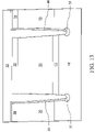
- FIGS. 1-3 are sequential vertical cross-sectional views of an exemplary structure according to the first and second embodiments of the present invention.
- FIGS. 4-10 are sequential vertical cross-sectional views of an exemplary structure according to the first embodiment of the present invention.
- FIGS. 11-17 are sequential vertical cross-sectional views of an exemplary structure according to the second embodiment of the present invention.
- the present invention relates to semiconductor structures with a far subcollector and a deep trench based far subcollector reachthrough and methods of manufacturing the same, which are now described in detail with accompanying figures.
- FIG. 1 a vertical cross-sectional view of an initial semiconductor substrate 10 is shown.
- a photoresist 5 is applied to a top surface of the initial semiconductor substrate 10 and lithographically patterned to define an opening in the photoresist 5 .
- Ion implantation is performed into an exposed portion of the initial semiconductor substrate 10 to form an implanted doped region 11 .
- FIG. 1 shows the implanted doped region 11 that extends to a surface of the initial semiconductor substrate 10
- formation of the implanted doped region 11 beneath the surface of the initial semiconductor substrate 10 may alternatively be performed with corresponding changes in the subsequent structures, which is explicitly contemplated herein.
- the doping of the implanted doped region 11 may be p-type or n-type.
- the doping concentrations is in the range from about 1.0 ⁇ 10 20 /cm 3 to about 5.0 ⁇ 10 21 /cm 3 , and preferably in the range from about 3.0 ⁇ 10 20 /cm 3 to about 2.0 ⁇ 10 21 /cm 3 to achieve low resistivity typically on the order of about 1.0 ⁇ 10 ⁇ 3 ⁇ -cm or less in the implanted doped region 11 .
- the patterned photoresist 5 is thereafter removed.
- a suitable surface clean such as a wet etch in a hydrofluoric acid (HF)
- an epitaxial growth of a semiconductor material is performed to form an epitaxially grown semiconductor portion 20 .
- the implanted doped region 11 is buried underneath the epitaxially grown semiconductor portion 20 to form a far subcollector 12 .
- the dopants in the implanted doped region 11 are subjected to bulk diffusion, and consequently, the thickness of the far subcollector 12 in FIG. 2 typically exceeds the thickness of the implanted doped region 11 in FIG. 1 .
- the initial semiconductor substrate 10 and the epitaxially grown semiconductor portion 20 collectively form a semiconductor substrate 24 , within which a far subcollector 12 is embedded.
- the initial semiconductor substrate 10 and the epitaxially grown semiconductor portion 20 may comprise the same or different semiconductor materials provided that the lattice mismatch between the two materials is small enough to allow epitaxial growth of the epitaxially grown semiconductor portion 20 on the initial semiconductor substrate 10 .
- semiconductor materials comprising each of the initial semiconductor substrate 10 and the epitaxially grown semiconductor portion 20 may be one of the following: silicon, germanium, silicon-germanium alloy, silicon carbon alloy, silicon-germanium-carbon alloy, gallium arsenide, indium arsenide, indium phosphide, III-V compound semiconductor materials, II-VI compound semiconductor materials, organic semiconductor materials, and other compound semiconductor materials.
- the doping concentrations of both the initial semiconductor substrate 10 and the epitaxially grown semiconductor portion 20 are low enough to prevent a high level of leakage current through the semiconductor material itself.
- the doping concentrations may be below 5.0 ⁇ 10 17 /cm 3 , and preferably below 1.0 ⁇ 10 16 /cm 3 in both the initial semiconductor substrate 10 and the epitaxially grown semiconductor portion 20 .
- a pad layer 30 is deposited on the semiconductor substrate 24 .
- the pad layer 30 may comprise a silicon oxide layer, a silicon nitride layer, or a stack of a silicon oxide layer and a silicon nitride layer.
- At least one deep trench 31 is formed in the semiconductor substrate 24 by applying and lithographically patterning a photoresist (not shown) and transferring the pattern in the photoresist into the optional pad layer 30 and into the semiconductor substrate 24 .
- the method of forming deep trenches with a depth exceeding 2.0 micron is well known in the art.
- the deep trenches may be formed with a depth in the range from about 2.0 micron to about 8.0 micron.
- At least a wall of the at least one deep trench 31 adjoins the far subcollector 12 , i.e., the at least one deep trench 31 intersects the far subcollector 12 during the etching of the at least one deep trench 31 .
- a guard ring region 32 may be formed directly beneath the at least one deep trench 31 by implanting dopants of the opposite conductivity type than the dopants in the far subcollector 12 .
- the ion implantation may be performed either after removing the photoresist for deep trench etch, or preferably, prior to removing the photoresist so that only the bottom of the at least one deep trench 31 is implanted with the dopants during the ion implantation.
- the guard ring region 32 having the opposite dopant type than the far subcollector 12 or a reachthrough region to be subsequently formed, provides a p-n junction so that latch up may be prevented.
- the dopant concentration in the guard ring region 32 is high enough such that outdiffusion of dopants from a doped material layer to be subsequently performed does not reverse the polarity of the doping type within the guard ring region 32 .
- the doping concentration in the guard ring region 32 is in the range from about 1.0 ⁇ 10 20 /cm 3 to about 5.0 ⁇ 10 21 /cm 3 , and preferably in the range from about 5.0 ⁇ 10 20 /cm 3 to about 2.0 ⁇ 10 20 /cm 3
- a doped material layer 50 is deposited on the walls of the at least one deep trench 31 as shown in FIG. 4 . If the optional pad layer 30 is present, the doped material layer 50 is also deposited on the optional pad layer 30 as well.
- the dopants within the doped material layer 50 are of the same conductivity type as the dopants in the far subcollector 12 .
- the doped material layer 50 may be selected from the group consisting of borosilicate glass (BSG), phosphosilicate glass (PSG), and arsenosilicate glass (ASG).
- the doped material layer may be selected from the group consisting of doped polysilicon, doped amorphous silicon, doped polycrystalline silicon containing alloy, and doped amorphous silicon containing alloy.
- a thermal anneal is performed to drive in the dopants from the doped material layer 50 into the semiconductor substrate 24 to form a reachthrough region 54 .
- Methods of performing a drive-in anneal are well known in the prior art.
- Dopants within the reachthrough region 54 are of the same conductivity type as the dopants in the far subcollector 12 , but are of the opposite conductivity type to the dopants in the guard ring region 32 .
- the peak doping concentration within the reachthrough region 54 is in the range from about 1.0 ⁇ 10 19 /cm 3 to about 1.0 ⁇ 10 21 /cm 3 , and preferably in the range from about 5.0 ⁇ 10 19 /cm 3 to about 5.0 ⁇ 10 20 /cm 3 , with a gradual radial decrease in the doping concentration from the center of the at least one deep trench 31 . Due to sufficiently high level of dopants in the guard ring region 32 , the guard ring region 32 maintains the same type of doping after the drive-in anneal.
- the reachthrough region 54 according to the first embodiment of the present invention may have a shape of a tapered cylinder, and may therefore be topologically homeomorphic to a torus, i.e., the reachthrough region may be transformed into a torus by continuous stretching and bending. If the guard ring region 32 is not formed, the reachthrough region 54 according to the first embodiment of the present invention may have a shape of a cup, and may therefore be topologically homeomorphic to a sphere, i.e., the reachthrough region may be transformed into a sphere by continuous stretching and bending. While the description of the present invention refers to “a reachthrough region” 54 , implementation of the present invention to multiple reachthrough regions 54 is straightforward and is herein explicitly contemplated. Multiple reachthrough regions 54 may be adjoined among themselves as needed.
- a dielectric layer 62 is formed on a wall of the at least one deep trench 31 .
- the dielectric layer 62 may be the remainder of the doped material layer 50 after the drive-in anneal if the doped material layer 50 is selected from the group consisting of borosilicate glass (BSG), phosphosilicate glass (PSG), and arsenosilicate glass (ASG).
- the dielectric layer 62 may be formed by oxidizing or nitridating the doped material layer 50 after the drive-in anneal if the doped material layer 50 is selected from the group consisting of doped polysilicon, doped amorphous silicon, doped polycrystalline silicon containing alloy, and doped amorphous silicon containing alloy.
- the dielectric layer 62 may be deposited, for example, by chemical vapor deposition (CVD) or alternating layer deposition (ALD), after removing the doped material layer 50 .
- the dielectric layer 62 is an insulator that does not conduct electricity.
- a fill material 64 fills the at least one deep trench 31 .
- the fill material 64 may be doped or undoped, and may comprise polysilicon, amorphous silicon, polycrystalline silicon containing alloy, or an amorphous silicon containing alloy. Further, the fill material 64 may comprise a dielectric material, for example, silicon oxide, silicon nitride, or silicon oxynitride.
- the fill material 64 may be a conductor or an insulator.
- the fill material 64 has conformal step coverage, and forms a minimal size seam at the center of the at least one deep trench 31 .
- the fill material 64 is either recessed by an etch, for example, a wet etch or a reactive ion etch (RIE), or planarized by chemical mechanical planarization (CMP). If the optional pad layer 30 is present, the optional pad layer 30 may be used as an etch stop layer or as a CMP stop layer. Thereafter, the optional pad layer 30 may be removed. Due to a finite thickness in the optional pad layer 30 , a pillar comprising a portion of the dielectric layer 62 and a portion of the fill material 64 may protrude from the surface of the semiconductor substrate 24 . Such protrusions may be reduced or eliminated by employing a reactive ion etch that recesses the dielectric layer 62 and the fill material 64 .
- RIE reactive ion etch
- CMP chemical mechanical planarization
- shallow trench isolation 70 is formed by conventional methods, e.g., by application and lithographic patterning of a photoresist (not shown), etching shallow trenches in the semiconductor substrate 24 , filling the shallow trenches with an insulator, and planarizing the top surface of the resulting semiconductor structure.
- the area for secondary reachthrough region 72 as seen from the top of the semiconductor substrate 24 , may be defined solely by a block mask or by a block mask in combination with the shallow trench isolation 70 .
- the depth of the secondary reachthrough region 72 is defined by the energy and implant species of the ion implantation, and may be higher than, lower than, or of the same height as the bottom of shallow trench isolation 70 .
- the secondary reachthrough region 72 partially overlaps the original reachthrough region 54 , or adjoins the reduced reachthrough region 54 ′ (hereafter referred to as reachthrough region 54 ′) that excludes the overlapping area between the secondary reachthrough region 72 and the original reachthrough region 54 .
- the dopants in the secondary reach through region 72 are of the same conductivity type as the dopants in the far subcollector 12 .
- Doped regions 74 other than the secondary reachthrough region 72 may also be formed at this point by suitable patterning of a photoresist (not shown) and ion implantation.
- a doped region 74 is formed in an epitaxially grown semiconductor portion 20 surrounded by the at least one deep trenches 31 and has the opposite type of doping to the doping of the far subcollector 12 , the overall structure forms a PIN diode.
- a metal contact 80 is preferably formed on the secondary reachthrough 80 .
- Metal contacts 80 may also be formed on other structures such as a doped region 74 .
- Metal contacts may comprise a metal silicide.
- a middle-of-line (MOL) dielectric 88 is thereafter deposited and planarized followed by formation of contact via holes that are subsequently filled with contact vias 90 .
- Metal wiring 92 is connected to the contact vias 90 .
- a dielectric layer 40 is deposited on the walls of the at least one deep trench 31 as shown in FIG. 11 . If the optional pad layer 30 is present, the dielectric layer 40 is also deposited on the optional pad layer 30 as well.
- the dielectric layer 40 preferably blocks diffusion of dopants.
- the dielectric layer 40 may comprise a silicon oxide layer, silicon nitride layer, a silicon oxynitride layer, or a stack thereof.
- the dielectric layer 40 comprises a silicon nitride layer.
- a photoresist 41 is applied to the top surface of the semiconductor substrate 24 and patterned such that only a portion of each of the at least one deep trench 31 is masked by the photoresist 41 while the remaining portion of each of the at least one deep trench 31 is exposed.
- the exposed portion of the at least one deep trench 31 is etched either by a wet etch or by a reactive ion etch (RIE).
- RIE reactive ion etch
- the wet etch or the reactive ion etch is selective to the underlying semiconductor material in the semiconductor substrate 24 and to the optional pad layer 30 .
- a doped material layer 52 is deposited within the at least one deep trench 31 and fills the at least one deep trench 31 as shown in FIG. 13 .
- the doped material layer 52 is a conductor. If the optional pad layer 30 is present, the doped material layer 52 is also deposited on the optional pad layer 30 as well.
- the dopants within the doped material layer 52 are of the same conductivity type as the dopants in the far subcollector 12 .
- the doped material layer 52 may be selected from the group consisting of doped polysilicon, doped amorphous silicon, doped polycrystalline silicon containing alloy, and doped amorphous silicon containing alloy.
- the doped material layer 52 has conformal step coverage and forms a minimal size seam at the center of the at least one deep trench 31 .
- the doped material layer 52 is either recessed by an etch, for example, a wet etch or a reactive ion etch (RIE), or planarized by chemical mechanical planarization (CMP) to form a doped fill material 52 ′.
- the dielectric layer 40 may be used as an etch stop layer or as a CMP stop layer. If the optional pad layer 30 is present, the optional pad layer 30 may also be used as an etch stop layer or as a CMP stop layer.
- a reactive ion etch may be employed to recesses the top of the doped fill material 52 ′ below the top surface of the optional pad layer 30 as shown in FIG. 14 .
- a thermal anneal is performed to drive in the dopants from the doped material layer 52 into the semiconductor substrate 24 to form a reachthrough region 54 . Since one side of the at least one deep trench 31 has the dielectric layer 40 that does not let dopants diffuse through, only the side of the at least one deep trench 31 without the dielectric layer 40 allows outdiffusion of dopants. Therefore, the reachthrough region 54 is formed only on one side of the at least one deep trench 31 . Dopants within the reachthrough region 54 are of the same conductivity type as the dopants in the far subcollector 12 , but are of the opposite conductivity type to the dopants in the guard ring region 32 .
- the peak doping concentration within the reachthrough region 54 is in the range from about 1.0 ⁇ 10 19 /cm 3 to about 1.0 ⁇ 10 21 /cm 3 , and preferably in the range from about 5.0 ⁇ 10 19 /cm 3 to about 5.0 ⁇ 10 20 /cm 3 , with a gradual radial decrease in the doping concentration from the center of the at least one deep trench 31 . Due to sufficiently high level of dopants in the guard ring region 32 , the guard ring region 32 maintains the same conductivity type of doping after the drive-in anneal.
- the reachthrough region 54 is formed only on one side of the at least one deep trench 31 , and may have a shape of a partial tapered cylinder that is cleaved along the length of a cylinder, and may therefore be topologically homeomorphic to a sphere. While the description of the present invention refers to “a reachthrough region” 54 , implementation of the present invention to multiple reachthrough regions 54 is straightforward and is herein explicitly contemplated. Multiple reachthrough regions 54 may be adjoined among themselves as needed.
- the portion of the dielectric layer 40 above the top surface of the semiconductor substrate 24 and the optional pad layer 30 are removed by a reactive ion etch (RIE) or preferably by a wet etch.
- RIE reactive ion etch
- shallow trench isolations 70 is formed by conventional methods, e.g., by application and lithographic patterning of a photoresist (not shown), etching shallow trenches in the semiconductor substrate 24 , filling the shallow trenches with an insulator, and planarizing the top surface of the resulting semiconductor structure.
- the shallow trench isolation 70 does not cover a portion of a top surface of the at least one deep trench 31 so that metal contacts may be subsequently formed thereupon.
- Doped regions 74 other than the secondary reachthrough region 72 may also be formed at this point by suitable pattering of a photoresist and ion implantation.
- a doped region 74 is formed in an epitaxially grown semiconductor portion 20 surrounded by the at least one deep trenches 31 and has the opposite type of doping that the doping of the far subcollector 12 , the overall structure forms a PIN diode.
- a metal contact 80 is preferably formed on the doped fill material 52 ′.
- Metal contacts 80 may also be formed on other structures such as a doped region 74 .
- Metal contacts may comprise a metal silicide.
- a middle-of-line (MOL) dielectric 88 is thereafter deposited and planarized followed by formation of contact via holes that are subsequently filled with contact vias 90 .
- Metal wiring 92 is connected to the contact vias 90 .
- a conductive path is formed from a far subcollector 12 that is preferably buried at a depth greater than projected ranges of conventional ion implantation through a reachthrough region ( 54 or 54 ′) that contacts the far subcollector and optionally through secondary reachthrough region 72 to a metal contact 80 on the surface of a semiconductor substrate 24 .
Abstract
Description
Claims (9)
Priority Applications (3)
| Application Number | Priority Date | Filing Date | Title |
|---|---|---|---|
| US11/680,637 US7691734B2 (en) | 2007-03-01 | 2007-03-01 | Deep trench based far subcollector reachthrough |
| CN2008100822617A CN101257039B (en) | 2007-03-01 | 2008-02-29 | Semiconductor structure and manufacturing method thereof |
| US12/691,320 US8105924B2 (en) | 2007-03-01 | 2010-01-21 | Deep trench based far subcollector reachthrough |
Applications Claiming Priority (1)
| Application Number | Priority Date | Filing Date | Title |
|---|---|---|---|
| US11/680,637 US7691734B2 (en) | 2007-03-01 | 2007-03-01 | Deep trench based far subcollector reachthrough |
Related Child Applications (1)
| Application Number | Title | Priority Date | Filing Date |
|---|---|---|---|
| US12/691,320 Division US8105924B2 (en) | 2007-03-01 | 2010-01-21 | Deep trench based far subcollector reachthrough |
Publications (2)
| Publication Number | Publication Date |
|---|---|
| US20080211064A1 US20080211064A1 (en) | 2008-09-04 |
| US7691734B2 true US7691734B2 (en) | 2010-04-06 |
Family
ID=39732477
Family Applications (2)
| Application Number | Title | Priority Date | Filing Date |
|---|---|---|---|
| US11/680,637 Expired - Fee Related US7691734B2 (en) | 2007-03-01 | 2007-03-01 | Deep trench based far subcollector reachthrough |
| US12/691,320 Expired - Fee Related US8105924B2 (en) | 2007-03-01 | 2010-01-21 | Deep trench based far subcollector reachthrough |
Family Applications After (1)
| Application Number | Title | Priority Date | Filing Date |
|---|---|---|---|
| US12/691,320 Expired - Fee Related US8105924B2 (en) | 2007-03-01 | 2010-01-21 | Deep trench based far subcollector reachthrough |
Country Status (2)
| Country | Link |
|---|---|
| US (2) | US7691734B2 (en) |
| CN (1) | CN101257039B (en) |
Cited By (5)
| Publication number | Priority date | Publication date | Assignee | Title |
|---|---|---|---|---|
| US20090224339A1 (en) * | 2008-03-04 | 2009-09-10 | Hvvi Semiconductors, Inc. | Silicon-Germanium-Carbon Semiconductor Structure |
| US20140141608A1 (en) * | 2006-06-28 | 2014-05-22 | Infineon Technologies Ag | Semiconductor component and methods for producing a semiconductor component |
| US10504768B1 (en) * | 2018-06-28 | 2019-12-10 | Globalfoundries Singapore Pte. Ltd. | Contact structures to deep trench isolation structures and method of nanufacturing the same |
| US11049932B2 (en) | 2018-12-20 | 2021-06-29 | Globalfoundries U.S. Inc. | Semiconductor isolation structures comprising shallow trench and deep trench isolation |
| US20220350041A1 (en) * | 2019-09-09 | 2022-11-03 | Semiconductor Components Industries, Llc | Silicon photomultipliers with split microcells |
Families Citing this family (21)
| Publication number | Priority date | Publication date | Assignee | Title |
|---|---|---|---|---|
| ITMI20072340A1 (en) * | 2007-12-14 | 2009-06-15 | St Microelectronics Srl | DEEP GUARD REGIONS IMPROVED TO REDUCE LATCH-UP IN ELECTRONIC DEVICES |
| ITMI20072341A1 (en) | 2007-12-14 | 2009-06-15 | St Microelectronics Srl | DEPTH CONTACTS OF INTEGRATED ELECTRONIC DEVICES BASED ON REGIONS PLANTED THROUGH SHEARS |
| US8105911B2 (en) * | 2008-09-30 | 2012-01-31 | Northrop Grumman Systems Corporation | Bipolar junction transistor guard ring structures and method of fabricating thereof |
| CN102403256B (en) * | 2010-09-08 | 2014-02-26 | 上海华虹宏力半导体制造有限公司 | Buried layer and manufacturing method, long hole contact and triode |
| US8912574B2 (en) | 2010-12-14 | 2014-12-16 | International Business Machines Corporation | Device isolation with improved thermal conductivity |
| CN102412308A (en) * | 2011-09-02 | 2012-04-11 | 上海华虹Nec电子有限公司 | Parasitic PIN device in BiCMOS (bipolar complementary metal oxide semiconductor) process and manufacturing method |
| CN103094313B (en) * | 2011-11-01 | 2016-08-17 | 上海华虹宏力半导体制造有限公司 | Parasitic N-I-P type PIN device structure in a kind of BICMOS technique and manufacture method thereof |
| CN102412287B (en) * | 2011-11-08 | 2013-07-24 | 上海华虹Nec电子有限公司 | Silicon-germanium HBT (heterojunction bipolar transistor) device and fabrication method thereof |
| CN103094329B (en) * | 2011-11-08 | 2016-02-10 | 上海华虹宏力半导体制造有限公司 | There is germanium silicium HBT device and the manufacture method thereof of dark counterfeit buried regions |
| CN103107186B (en) * | 2011-11-11 | 2016-06-08 | 上海华虹宏力半导体制造有限公司 | Parasitic N-I-P type PIN device structure and manufacture method thereof in a kind of BiCMOS technique |
| CN103178121B (en) * | 2011-12-21 | 2015-06-03 | 上海华虹宏力半导体制造有限公司 | Pin diode and manufacturing method thereof |
| US8766235B2 (en) * | 2012-03-08 | 2014-07-01 | Micron Technology, Inc. | Bipolar junction transistors and memory arrays |
| US9406742B2 (en) * | 2014-04-09 | 2016-08-02 | Vanguard International Semiconductor Corporation | Semiconductor device having super-junction structures |
| EP3024020A1 (en) * | 2014-11-19 | 2016-05-25 | Nxp B.V. | Semiconductor device and method |
| US10134830B2 (en) * | 2016-09-13 | 2018-11-20 | Texas Instruments Incorporated | Integrated trench capacitor |
| CN108054094A (en) * | 2017-12-18 | 2018-05-18 | 深圳市晶特智造科技有限公司 | Bipolar transistor and preparation method thereof |
| FR3087048B1 (en) * | 2018-10-08 | 2021-11-12 | St Microelectronics Sa | BIPOLAR TRANSISTOR |
| US11031241B2 (en) * | 2018-12-20 | 2021-06-08 | Applied Materials, Inc. | Method of growing doped group IV materials |
| JP7279393B2 (en) * | 2019-02-15 | 2023-05-23 | 富士電機株式会社 | Manufacturing method of semiconductor integrated circuit |
| CN110416152A (en) * | 2019-07-26 | 2019-11-05 | 上海华虹宏力半导体制造有限公司 | Deep groove isolation structure and process |
| CN110518030A (en) * | 2019-09-24 | 2019-11-29 | 德淮半导体有限公司 | Semiconductor device and its manufacturing method |
Citations (93)
| Publication number | Priority date | Publication date | Assignee | Title |
|---|---|---|---|---|
| US3386865A (en) * | 1965-05-10 | 1968-06-04 | Ibm | Process of making planar semiconductor devices isolated by encapsulating oxide filled channels |
| US3648125A (en) * | 1971-02-02 | 1972-03-07 | Fairchild Camera Instr Co | Method of fabricating integrated circuits with oxidized isolation and the resulting structure |
| US3841917A (en) * | 1971-09-06 | 1974-10-15 | Philips Nv | Methods of manufacturing semiconductor devices |
| US3947299A (en) * | 1971-05-22 | 1976-03-30 | U.S. Philips Corporation | Method of manufacturing semiconductor devices |
| US4236294A (en) | 1979-03-16 | 1980-12-02 | International Business Machines Corporation | High performance bipolar device and method for making same |
| US4243435A (en) | 1979-06-22 | 1981-01-06 | International Business Machines Corporation | Bipolar transistor fabrication process with an ion implanted emitter |
| US4272776A (en) * | 1971-05-22 | 1981-06-09 | U.S. Philips Corporation | Semiconductor device and method of manufacturing same |
| US4353086A (en) * | 1980-05-07 | 1982-10-05 | Bell Telephone Laboratories, Incorporated | Silicon integrated circuits |
| US4466180A (en) * | 1981-06-25 | 1984-08-21 | Rockwell International Corporation | Method of manufacturing punch through voltage regulator diodes utilizing shaping and selective doping |
| US4470062A (en) * | 1979-08-31 | 1984-09-04 | Hitachi, Ltd. | Semiconductor device having isolation regions |
| US4503451A (en) * | 1982-07-30 | 1985-03-05 | Motorola, Inc. | Low resistance buried power bus for integrated circuits |
| US4519128A (en) * | 1983-10-05 | 1985-05-28 | International Business Machines Corporation | Method of making a trench isolated device |
| US4528047A (en) * | 1984-06-25 | 1985-07-09 | International Business Machines Corporation | Method for forming a void free isolation structure utilizing etch and refill techniques |
| US4546538A (en) * | 1983-09-05 | 1985-10-15 | Oki Electric Industry Co., Ltd. | Method of manufacturing semiconductor integrated circuit devices having dielectric isolation regions |
| US4549927A (en) * | 1984-06-29 | 1985-10-29 | International Business Machines Corporation | Method of selectively exposing the sidewalls of a trench and its use to the forming of a metal silicide substrate contact for dielectric filled deep trench isolated devices |
| US4638552A (en) * | 1984-05-09 | 1987-01-27 | Kabushiki Kaisha Toshiba | Method of manufacturing semiconductor substrate |
| US4672410A (en) * | 1984-07-12 | 1987-06-09 | Nippon Telegraph & Telephone | Semiconductor memory device with trench surrounding each memory cell |
| US4689656A (en) * | 1984-06-25 | 1987-08-25 | International Business Machines Corporation | Method for forming a void free isolation pattern and resulting structure |
| US4704368A (en) * | 1985-10-30 | 1987-11-03 | International Business Machines Corporation | Method of making trench-incorporated monolithic semiconductor capacitor and high density dynamic memory cells including the capacitor |
| US4712125A (en) * | 1982-08-06 | 1987-12-08 | International Business Machines Corporation | Structure for contacting a narrow width PN junction region |
| US4711017A (en) * | 1986-03-03 | 1987-12-08 | Trw Inc. | Formation of buried diffusion devices |
| US4713358A (en) * | 1986-05-02 | 1987-12-15 | Gte Laboratories Incorporated | Method of fabricating recessed gate static induction transistors |
| US4717682A (en) * | 1985-02-20 | 1988-01-05 | Kabushiki Kaisha Toshiba | Method of manufacturing a semiconductor device with conductive trench sidewalls |
| US4719185A (en) * | 1986-04-28 | 1988-01-12 | International Business Machines Corporation | Method of making shallow junction complementary vertical bipolar transistor pair |
| US4725562A (en) * | 1986-03-27 | 1988-02-16 | International Business Machines Corporation | Method of making a contact to a trench isolated device |
| US4810668A (en) * | 1986-07-18 | 1989-03-07 | Kabushiki Kaisha Toshiba | Semiconductor device element-isolation by oxidation of polysilicon in trench |
| US4819052A (en) * | 1986-12-22 | 1989-04-04 | Texas Instruments Incorporated | Merged bipolar/CMOS technology using electrically active trench |
| US4835115A (en) * | 1987-12-07 | 1989-05-30 | Texas Instruments Incorporated | Method for forming oxide-capped trench isolation |
| US4868631A (en) * | 1985-11-18 | 1989-09-19 | Texas Instruments Incorporated | Bipolar transistor with shallow junctions and capable of high packing density |
| US4871685A (en) * | 1987-08-13 | 1989-10-03 | Kabushiki Kaisha Toshiba | Method of manufacturing bipolar transistor with self-aligned external base and emitter regions |
| US4910572A (en) * | 1985-07-19 | 1990-03-20 | Matsushita Electric Industrial Co., Ltd. | Semiconductor device and method of fabricating the same |
| US4910567A (en) * | 1986-02-26 | 1990-03-20 | Texas Instruments, Incorporated | Dram cell and method for fabricating |
| US4963505A (en) * | 1987-10-27 | 1990-10-16 | Nippondenso Co., Ltd. | Semiconductor device and method of manufacturing same |
| US4980747A (en) * | 1986-12-22 | 1990-12-25 | Texas Instruments Inc. | Deep trench isolation with surface contact to substrate |
| US4984048A (en) * | 1987-07-10 | 1991-01-08 | Hitachi, Ltd. | Semiconductor device with buried side contact |
| US4992843A (en) * | 1986-12-18 | 1991-02-12 | Deutsche Itt Industries Gmbh | Collector contact of an integrated bipolar transistor |
| US5003365A (en) * | 1988-06-09 | 1991-03-26 | Texas Instruments Incorporated | Bipolar transistor with a sidewall-diffused subcollector |
| US5008208A (en) * | 1988-12-07 | 1991-04-16 | Honeywell Inc. | Method of making planarized, self-aligned bipolar integrated circuits |
| US5026658A (en) * | 1985-07-02 | 1991-06-25 | Matsushita Electric Industrial Co., Ltd. | Method of making a trench capacitor dram cell |
| US5072269A (en) * | 1988-03-15 | 1991-12-10 | Kabushiki Kaisha Toshiba | Dynamic ram and method of manufacturing the same |
| US5105253A (en) * | 1988-12-28 | 1992-04-14 | Synergy Semiconductor Corporation | Structure for a substrate tap in a bipolar structure |
| US5106777A (en) * | 1989-09-27 | 1992-04-21 | Texas Instruments Incorporated | Trench isolation process with reduced topography |
| US5108783A (en) * | 1988-12-23 | 1992-04-28 | Sharp Kabushiki Kaisha | Process for producing semiconductor devices |
| US5110749A (en) * | 1990-06-22 | 1992-05-05 | Mitsubishi Denki Kabushiki Kaisha | Method for manufacturing semiconductor device |
| US5241210A (en) * | 1987-02-26 | 1993-08-31 | Kabushiki Kaisha Toshiba | High breakdown voltage semiconductor device |
| US5250837A (en) * | 1991-05-17 | 1993-10-05 | Delco Electronics Corporation | Method for dielectrically isolating integrated circuits using doped oxide sidewalls |
| US5306940A (en) * | 1990-10-22 | 1994-04-26 | Nec Corporation | Semiconductor device including a locos type field oxide film and a U trench penetrating the locos film |
| US5340753A (en) | 1990-10-31 | 1994-08-23 | International Business Machines Corp. | Method for fabricating self-aligned epitaxial base transistor |
| US5411898A (en) * | 1991-03-13 | 1995-05-02 | Mitsubishi Denki Kabushiki Kaisha | Method of manufacturing a complementary bipolar transistor |
| US5420061A (en) * | 1993-08-13 | 1995-05-30 | Micron Semiconductor, Inc. | Method for improving latchup immunity in a dual-polysilicon gate process |
| US5534450A (en) * | 1994-05-04 | 1996-07-09 | Hyundai Electronics Industries Co., Ltd. | Method for fabrication a semiconductor device |
| US5541120A (en) * | 1992-01-31 | 1996-07-30 | Analog Devices, Inc. | Method of making complementary bipolar polysilicon emitter devices |
| US5541440A (en) * | 1993-07-28 | 1996-07-30 | Mitsubishi Denki Kabushiki Kaisha | Isolation structure for semiconductor device |
| US5770504A (en) * | 1997-03-17 | 1998-06-23 | International Business Machines Corporation | Method for increasing latch-up immunity in CMOS devices |
| US5856700A (en) * | 1996-05-08 | 1999-01-05 | Harris Corporation | Semiconductor device with doped semiconductor and dielectric trench sidewall layers |
| US5859459A (en) * | 1996-04-03 | 1999-01-12 | Sony Corporation | Semiconductor memory device and method of manufacturing the same |
| US6056392A (en) * | 1989-12-11 | 2000-05-02 | Canon Kabushiki Kaisha | Method of producing recording head |
| US6097076A (en) * | 1997-03-25 | 2000-08-01 | Micron Technology, Inc. | Self-aligned isolation trench |
| US6104078A (en) * | 1994-03-09 | 2000-08-15 | Denso Corporation | Design for a semiconductor device having elements isolated by insulating regions |
| US6121668A (en) * | 1997-03-27 | 2000-09-19 | Telefonaktiebolaget Lm Ericsson | Semiconductor device provided with conductor electrically connected to conducting region |
| US6144086A (en) * | 1999-04-30 | 2000-11-07 | International Business Machines Corporation | Structure for improved latch-up using dual depth STI with impurity implant |
| US6184565B1 (en) * | 1992-01-27 | 2001-02-06 | Harris Corporation | Biasing of island-surrounding material to suppress reduction of breakdown voltage due to field plate acting on buried layer/island junction between high and low impurity concentration regions |
| US6207493B1 (en) * | 1998-08-19 | 2001-03-27 | International Business Machines Corporation | Formation of out-diffused bitline by laser anneal |
| US6242770B1 (en) * | 1998-08-31 | 2001-06-05 | Gary Bela Bronner | Diode connected to a magnetic tunnel junction and self aligned with a metallic conductor and method for forming the same |
| US6255689B1 (en) * | 1999-12-20 | 2001-07-03 | United Microelectronics Corp. | Flash memory structure and method of manufacture |
| US6406972B2 (en) * | 1997-05-23 | 2002-06-18 | Telefonaktiebolaget Lm Ericsson | Integrated circuit, components thereof and manufacturing method |
| US20020084506A1 (en) * | 2000-12-29 | 2002-07-04 | International Business Machines Corporation | Deep trench-buried layer array and integrated device structures for noise isolation and latch up immunity |
| US6426526B1 (en) * | 2000-06-23 | 2002-07-30 | International Business Machines Corporation | Single sided buried strap |
| US20020130392A1 (en) * | 2001-03-19 | 2002-09-19 | International Business Machines Corporation | Internally ballasted silicon germanium transistor |
| US6455902B1 (en) * | 2000-12-06 | 2002-09-24 | International Business Machines Corporation | BiCMOS ESD circuit with subcollector/trench-isolated body mosfet for mixed signal analog/digital RF applications |
| US6465304B1 (en) * | 2001-10-04 | 2002-10-15 | General Semiconductor, Inc. | Method for fabricating a power semiconductor device having a floating island voltage sustaining layer |
| US6538294B1 (en) * | 1999-06-23 | 2003-03-25 | Telefonaktiebolaget Lm Ericson (Publ) | Trenched semiconductor device with high breakdown voltage |
| US6586818B1 (en) * | 2002-03-08 | 2003-07-01 | International Business Machines Corporation | Self-aligned silicon germanium heterojunction bipolar transistor device with electrostatic discharge crevice cover for salicide displacement |
| US6605862B2 (en) * | 2001-02-22 | 2003-08-12 | Koninklijke Philips Electronics N.V. | Trench semiconductor devices |
| US6689672B2 (en) * | 2000-04-10 | 2004-02-10 | Stmicroelectronics S.A. | Buried layer manufacturing method |
| US6740954B2 (en) * | 2000-07-26 | 2004-05-25 | Samsung Electronics Co, Ltd. | Semiconductor device reducing junction leakage current and narrow width effect |
| US6750526B2 (en) * | 2001-11-22 | 2004-06-15 | Renesas Technology Corp. | Semiconductor device with trench isolation having reduced leak current |
| US6794250B2 (en) * | 2002-05-01 | 2004-09-21 | Nanya Technology Corporation | Vertical split gate flash memory cell and method for fabricating the same |
| US20040222486A1 (en) * | 2003-05-09 | 2004-11-11 | International Business Machines Corporation | BiCMOS TECHNOLOGY ON SOI SUBSTRATES |
| US6844239B2 (en) * | 2002-07-24 | 2005-01-18 | Samsung Electronics Co., Ltd. | Method for forming shallow well of semiconductor device using low-energy ion implantation |
| US20050014344A1 (en) * | 2003-07-18 | 2005-01-20 | Choi Myung Gyu | Method of forming well in semiconductor device |
| US6891251B2 (en) | 2001-12-13 | 2005-05-10 | International Business Machines Corporation | Varactors for CMOS and BiCMOS technologies |
| US20050225910A1 (en) | 2004-03-31 | 2005-10-13 | International Business Machines Corporation | Tunable esd trigger and power clamp circuit |
| US6989557B2 (en) * | 2002-06-05 | 2006-01-24 | United Microelectronics Corp. | Bipolar junction transistor and fabricating method |
| US6995449B1 (en) * | 2003-02-20 | 2006-02-07 | Newport Fab, Llc | Deep trench isolation region with reduced-size cavities in overlying field oxide |
| US7015115B1 (en) * | 2003-02-20 | 2006-03-21 | Newport Fab, Llc | Method for forming deep trench isolation and related structure |
| US7022573B2 (en) * | 2003-01-17 | 2006-04-04 | Nanya Technology Corporation | Stack gate with tip vertical memory and method for fabricating the same |
| US7071531B2 (en) * | 1999-01-14 | 2006-07-04 | Micron Technology, Inc. | Trench isolation for semiconductor devices |
| US20070048928A1 (en) * | 2004-08-31 | 2007-03-01 | Infineon Technologies Ag | Method in the fabrication of a monolithically integrated vertical device on an SOI substrate |
| US7442996B2 (en) * | 2006-01-20 | 2008-10-28 | International Business Machines Corporation | Structure and method for enhanced triple well latchup robustness |
| US7465969B2 (en) * | 2003-03-25 | 2008-12-16 | Panasonic Corporation | Bipolar transistor and method for fabricating the same |
| US7489016B2 (en) * | 2002-08-14 | 2009-02-10 | Advanced Analogic Technologies, Inc. | Trench-constrained isolation diffusion for integrated circuit die |
| US20090261312A1 (en) * | 2008-04-18 | 2009-10-22 | Qimonda Ag | Integrated circuit including an array of low resistive vertical diodes and method |
Family Cites Families (23)
| Publication number | Priority date | Publication date | Assignee | Title |
|---|---|---|---|---|
| US4066473A (en) * | 1976-07-15 | 1978-01-03 | Fairchild Camera And Instrument Corporation | Method of fabricating high-gain transistors |
| US4284997A (en) * | 1977-07-07 | 1981-08-18 | Zaidan Hojin Handotai Kenkyu Shinkokai | Static induction transistor and its applied devices |
| US4373252A (en) * | 1981-02-17 | 1983-02-15 | Fairchild Camera & Instrument | Method for manufacturing a semiconductor structure having reduced lateral spacing between buried regions |
| US4829017A (en) * | 1986-09-25 | 1989-05-09 | Texas Instruments Incorporated | Method for lubricating a high capacity dram cell |
| JPS63237460A (en) * | 1987-03-25 | 1988-10-03 | Mitsubishi Electric Corp | Semiconductor device |
| US5187554A (en) * | 1987-08-11 | 1993-02-16 | Sony Corporation | Bipolar transistor |
| US4791462A (en) * | 1987-09-10 | 1988-12-13 | Siliconix Incorporated | Dense vertical j-MOS transistor |
| US5258635A (en) * | 1988-09-06 | 1993-11-02 | Kabushiki Kaisha Toshiba | MOS-type semiconductor integrated circuit device |
| JP2517375B2 (en) * | 1988-12-19 | 1996-07-24 | 三菱電機株式会社 | Solid-state imaging device, charge transfer device used in the device, and manufacturing method thereof |
| US5064777A (en) * | 1990-06-28 | 1991-11-12 | International Business Machines Corporation | Fabrication method for a double trench memory cell device |
| JP2994110B2 (en) * | 1991-09-09 | 1999-12-27 | 株式会社東芝 | Semiconductor storage device |
| US5455190A (en) * | 1994-12-07 | 1995-10-03 | United Microelectronics Corporation | Method of making a vertical channel device using buried source techniques |
| EP0879481B1 (en) * | 1996-02-05 | 2002-05-02 | Infineon Technologies AG | Field effect controlled semiconductor component |
| EP0970518B1 (en) * | 1997-03-18 | 2012-04-25 | Infineon Technologies AG | Trench-isolated bipolar devices |
| US6246094B1 (en) * | 1998-10-20 | 2001-06-12 | Winbond Electronics Corporation | Buried shallow trench isolation and method for forming the same |
| DE19944012B4 (en) * | 1999-09-14 | 2007-07-19 | Infineon Technologies Ag | Trench capacitor with capacitor electrodes and corresponding manufacturing process |
| US6429099B1 (en) * | 2000-01-05 | 2002-08-06 | International Business Machines Corporation | Implementing contacts for bodies of semiconductor-on-insulator transistors |
| US7064416B2 (en) * | 2001-11-16 | 2006-06-20 | International Business Machines Corporation | Semiconductor device and method having multiple subcollectors formed on a common wafer |
| US6902982B2 (en) * | 2003-04-02 | 2005-06-07 | Promos Technologies Inc. | Trench capacitor and process for preventing parasitic leakage |
| US6946358B2 (en) * | 2003-05-30 | 2005-09-20 | International Business Machines Corporation | Method of fabricating shallow trench isolation by ultra-thin SIMOX processing |
| US7851860B2 (en) * | 2004-03-26 | 2010-12-14 | Honeywell International Inc. | Techniques to reduce substrate cross talk on mixed signal and RF circuit design |
| US20070057304A1 (en) * | 2005-09-12 | 2007-03-15 | Infineon Technologies Ag | Capacitor structure, memory cell and method for forming a capacitor structure |
| US7294543B2 (en) * | 2006-03-22 | 2007-11-13 | International Business Machines Corporation | DRAM (Dynamic Random Access Memory) cells |
-
2007
- 2007-03-01 US US11/680,637 patent/US7691734B2/en not_active Expired - Fee Related
-
2008
- 2008-02-29 CN CN2008100822617A patent/CN101257039B/en not_active Expired - Fee Related
-
2010
- 2010-01-21 US US12/691,320 patent/US8105924B2/en not_active Expired - Fee Related
Patent Citations (100)
| Publication number | Priority date | Publication date | Assignee | Title |
|---|---|---|---|---|
| US3386865A (en) * | 1965-05-10 | 1968-06-04 | Ibm | Process of making planar semiconductor devices isolated by encapsulating oxide filled channels |
| US3648125A (en) * | 1971-02-02 | 1972-03-07 | Fairchild Camera Instr Co | Method of fabricating integrated circuits with oxidized isolation and the resulting structure |
| US3947299A (en) * | 1971-05-22 | 1976-03-30 | U.S. Philips Corporation | Method of manufacturing semiconductor devices |
| US4272776A (en) * | 1971-05-22 | 1981-06-09 | U.S. Philips Corporation | Semiconductor device and method of manufacturing same |
| US3841917A (en) * | 1971-09-06 | 1974-10-15 | Philips Nv | Methods of manufacturing semiconductor devices |
| US4236294A (en) | 1979-03-16 | 1980-12-02 | International Business Machines Corporation | High performance bipolar device and method for making same |
| US4243435A (en) | 1979-06-22 | 1981-01-06 | International Business Machines Corporation | Bipolar transistor fabrication process with an ion implanted emitter |
| US4470062A (en) * | 1979-08-31 | 1984-09-04 | Hitachi, Ltd. | Semiconductor device having isolation regions |
| US4353086A (en) * | 1980-05-07 | 1982-10-05 | Bell Telephone Laboratories, Incorporated | Silicon integrated circuits |
| US4466180A (en) * | 1981-06-25 | 1984-08-21 | Rockwell International Corporation | Method of manufacturing punch through voltage regulator diodes utilizing shaping and selective doping |
| US4503451A (en) * | 1982-07-30 | 1985-03-05 | Motorola, Inc. | Low resistance buried power bus for integrated circuits |
| US4712125A (en) * | 1982-08-06 | 1987-12-08 | International Business Machines Corporation | Structure for contacting a narrow width PN junction region |
| US4546538A (en) * | 1983-09-05 | 1985-10-15 | Oki Electric Industry Co., Ltd. | Method of manufacturing semiconductor integrated circuit devices having dielectric isolation regions |
| US4519128A (en) * | 1983-10-05 | 1985-05-28 | International Business Machines Corporation | Method of making a trench isolated device |
| US4638552A (en) * | 1984-05-09 | 1987-01-27 | Kabushiki Kaisha Toshiba | Method of manufacturing semiconductor substrate |
| US4528047A (en) * | 1984-06-25 | 1985-07-09 | International Business Machines Corporation | Method for forming a void free isolation structure utilizing etch and refill techniques |
| US4689656A (en) * | 1984-06-25 | 1987-08-25 | International Business Machines Corporation | Method for forming a void free isolation pattern and resulting structure |
| US4549927A (en) * | 1984-06-29 | 1985-10-29 | International Business Machines Corporation | Method of selectively exposing the sidewalls of a trench and its use to the forming of a metal silicide substrate contact for dielectric filled deep trench isolated devices |
| US4672410A (en) * | 1984-07-12 | 1987-06-09 | Nippon Telegraph & Telephone | Semiconductor memory device with trench surrounding each memory cell |
| US4717682A (en) * | 1985-02-20 | 1988-01-05 | Kabushiki Kaisha Toshiba | Method of manufacturing a semiconductor device with conductive trench sidewalls |
| US5026658A (en) * | 1985-07-02 | 1991-06-25 | Matsushita Electric Industrial Co., Ltd. | Method of making a trench capacitor dram cell |
| US4910572A (en) * | 1985-07-19 | 1990-03-20 | Matsushita Electric Industrial Co., Ltd. | Semiconductor device and method of fabricating the same |
| US4704368A (en) * | 1985-10-30 | 1987-11-03 | International Business Machines Corporation | Method of making trench-incorporated monolithic semiconductor capacitor and high density dynamic memory cells including the capacitor |
| US4868631A (en) * | 1985-11-18 | 1989-09-19 | Texas Instruments Incorporated | Bipolar transistor with shallow junctions and capable of high packing density |
| US4910567A (en) * | 1986-02-26 | 1990-03-20 | Texas Instruments, Incorporated | Dram cell and method for fabricating |
| US4711017A (en) * | 1986-03-03 | 1987-12-08 | Trw Inc. | Formation of buried diffusion devices |
| US4725562A (en) * | 1986-03-27 | 1988-02-16 | International Business Machines Corporation | Method of making a contact to a trench isolated device |
| US4719185A (en) * | 1986-04-28 | 1988-01-12 | International Business Machines Corporation | Method of making shallow junction complementary vertical bipolar transistor pair |
| US4713358A (en) * | 1986-05-02 | 1987-12-15 | Gte Laboratories Incorporated | Method of fabricating recessed gate static induction transistors |
| US4810668A (en) * | 1986-07-18 | 1989-03-07 | Kabushiki Kaisha Toshiba | Semiconductor device element-isolation by oxidation of polysilicon in trench |
| US4992843A (en) * | 1986-12-18 | 1991-02-12 | Deutsche Itt Industries Gmbh | Collector contact of an integrated bipolar transistor |
| US4819052A (en) * | 1986-12-22 | 1989-04-04 | Texas Instruments Incorporated | Merged bipolar/CMOS technology using electrically active trench |
| US4980747A (en) * | 1986-12-22 | 1990-12-25 | Texas Instruments Inc. | Deep trench isolation with surface contact to substrate |
| US5241210A (en) * | 1987-02-26 | 1993-08-31 | Kabushiki Kaisha Toshiba | High breakdown voltage semiconductor device |
| US4984048A (en) * | 1987-07-10 | 1991-01-08 | Hitachi, Ltd. | Semiconductor device with buried side contact |
| US4871685A (en) * | 1987-08-13 | 1989-10-03 | Kabushiki Kaisha Toshiba | Method of manufacturing bipolar transistor with self-aligned external base and emitter regions |
| US4963505A (en) * | 1987-10-27 | 1990-10-16 | Nippondenso Co., Ltd. | Semiconductor device and method of manufacturing same |
| US4835115A (en) * | 1987-12-07 | 1989-05-30 | Texas Instruments Incorporated | Method for forming oxide-capped trench isolation |
| US5072269A (en) * | 1988-03-15 | 1991-12-10 | Kabushiki Kaisha Toshiba | Dynamic ram and method of manufacturing the same |
| US5003365A (en) * | 1988-06-09 | 1991-03-26 | Texas Instruments Incorporated | Bipolar transistor with a sidewall-diffused subcollector |
| US5008208A (en) * | 1988-12-07 | 1991-04-16 | Honeywell Inc. | Method of making planarized, self-aligned bipolar integrated circuits |
| US5108783A (en) * | 1988-12-23 | 1992-04-28 | Sharp Kabushiki Kaisha | Process for producing semiconductor devices |
| US5105253A (en) * | 1988-12-28 | 1992-04-14 | Synergy Semiconductor Corporation | Structure for a substrate tap in a bipolar structure |
| US5106777A (en) * | 1989-09-27 | 1992-04-21 | Texas Instruments Incorporated | Trench isolation process with reduced topography |
| US6056392A (en) * | 1989-12-11 | 2000-05-02 | Canon Kabushiki Kaisha | Method of producing recording head |
| US5110749A (en) * | 1990-06-22 | 1992-05-05 | Mitsubishi Denki Kabushiki Kaisha | Method for manufacturing semiconductor device |
| US5306940A (en) * | 1990-10-22 | 1994-04-26 | Nec Corporation | Semiconductor device including a locos type field oxide film and a U trench penetrating the locos film |
| US5340753A (en) | 1990-10-31 | 1994-08-23 | International Business Machines Corp. | Method for fabricating self-aligned epitaxial base transistor |
| US5411898A (en) * | 1991-03-13 | 1995-05-02 | Mitsubishi Denki Kabushiki Kaisha | Method of manufacturing a complementary bipolar transistor |
| US5250837A (en) * | 1991-05-17 | 1993-10-05 | Delco Electronics Corporation | Method for dielectrically isolating integrated circuits using doped oxide sidewalls |
| US6184565B1 (en) * | 1992-01-27 | 2001-02-06 | Harris Corporation | Biasing of island-surrounding material to suppress reduction of breakdown voltage due to field plate acting on buried layer/island junction between high and low impurity concentration regions |
| US5541120A (en) * | 1992-01-31 | 1996-07-30 | Analog Devices, Inc. | Method of making complementary bipolar polysilicon emitter devices |
| US5541440A (en) * | 1993-07-28 | 1996-07-30 | Mitsubishi Denki Kabushiki Kaisha | Isolation structure for semiconductor device |
| US5420061A (en) * | 1993-08-13 | 1995-05-30 | Micron Semiconductor, Inc. | Method for improving latchup immunity in a dual-polysilicon gate process |
| US6207512B1 (en) * | 1993-08-13 | 2001-03-27 | Micron Technology, Inc. | Method and apparatus for improving latchup immunity in a dual-polysilicon gate process |
| US6445044B2 (en) * | 1993-08-13 | 2002-09-03 | Micron Technology, Inc. | Apparatus improving latchup immunity in a dual-polysilicon gate |
| US6104078A (en) * | 1994-03-09 | 2000-08-15 | Denso Corporation | Design for a semiconductor device having elements isolated by insulating regions |
| US5534450A (en) * | 1994-05-04 | 1996-07-09 | Hyundai Electronics Industries Co., Ltd. | Method for fabrication a semiconductor device |
| US5859459A (en) * | 1996-04-03 | 1999-01-12 | Sony Corporation | Semiconductor memory device and method of manufacturing the same |
| US5856700A (en) * | 1996-05-08 | 1999-01-05 | Harris Corporation | Semiconductor device with doped semiconductor and dielectric trench sidewall layers |
| US5770504A (en) * | 1997-03-17 | 1998-06-23 | International Business Machines Corporation | Method for increasing latch-up immunity in CMOS devices |
| US6097076A (en) * | 1997-03-25 | 2000-08-01 | Micron Technology, Inc. | Self-aligned isolation trench |
| US6121668A (en) * | 1997-03-27 | 2000-09-19 | Telefonaktiebolaget Lm Ericsson | Semiconductor device provided with conductor electrically connected to conducting region |
| US6406972B2 (en) * | 1997-05-23 | 2002-06-18 | Telefonaktiebolaget Lm Ericsson | Integrated circuit, components thereof and manufacturing method |
| US6258661B1 (en) * | 1998-08-19 | 2001-07-10 | International Business Machines Corporation | Formation of out-diffused bitline by laser anneal |
| US6207493B1 (en) * | 1998-08-19 | 2001-03-27 | International Business Machines Corporation | Formation of out-diffused bitline by laser anneal |
| US6242770B1 (en) * | 1998-08-31 | 2001-06-05 | Gary Bela Bronner | Diode connected to a magnetic tunnel junction and self aligned with a metallic conductor and method for forming the same |
| US20010010938A1 (en) * | 1998-08-31 | 2001-08-02 | Bronner Gary Bela | Diode connected to a magnetic tunnel junction and self aligned with a metallic conductor and method of forming the same |
| US6562634B2 (en) * | 1998-08-31 | 2003-05-13 | International Business Machines Corporation | Diode connected to a magnetic tunnel junction and self aligned with a metallic conductor and method of forming the same |
| US7071531B2 (en) * | 1999-01-14 | 2006-07-04 | Micron Technology, Inc. | Trench isolation for semiconductor devices |
| US6144086A (en) * | 1999-04-30 | 2000-11-07 | International Business Machines Corporation | Structure for improved latch-up using dual depth STI with impurity implant |
| US6538294B1 (en) * | 1999-06-23 | 2003-03-25 | Telefonaktiebolaget Lm Ericson (Publ) | Trenched semiconductor device with high breakdown voltage |
| US6255689B1 (en) * | 1999-12-20 | 2001-07-03 | United Microelectronics Corp. | Flash memory structure and method of manufacture |
| US6689672B2 (en) * | 2000-04-10 | 2004-02-10 | Stmicroelectronics S.A. | Buried layer manufacturing method |
| US6426526B1 (en) * | 2000-06-23 | 2002-07-30 | International Business Machines Corporation | Single sided buried strap |
| US6573137B1 (en) * | 2000-06-23 | 2003-06-03 | International Business Machines Corporation | Single sided buried strap |
| US6740954B2 (en) * | 2000-07-26 | 2004-05-25 | Samsung Electronics Co, Ltd. | Semiconductor device reducing junction leakage current and narrow width effect |
| US6455902B1 (en) * | 2000-12-06 | 2002-09-24 | International Business Machines Corporation | BiCMOS ESD circuit with subcollector/trench-isolated body mosfet for mixed signal analog/digital RF applications |
| US20020084506A1 (en) * | 2000-12-29 | 2002-07-04 | International Business Machines Corporation | Deep trench-buried layer array and integrated device structures for noise isolation and latch up immunity |
| US6605862B2 (en) * | 2001-02-22 | 2003-08-12 | Koninklijke Philips Electronics N.V. | Trench semiconductor devices |
| US20020130392A1 (en) * | 2001-03-19 | 2002-09-19 | International Business Machines Corporation | Internally ballasted silicon germanium transistor |
| US6455919B1 (en) * | 2001-03-19 | 2002-09-24 | International Business Machines Corporation | Internally ballasted silicon germanium transistor |
| US6465304B1 (en) * | 2001-10-04 | 2002-10-15 | General Semiconductor, Inc. | Method for fabricating a power semiconductor device having a floating island voltage sustaining layer |
| US6750526B2 (en) * | 2001-11-22 | 2004-06-15 | Renesas Technology Corp. | Semiconductor device with trench isolation having reduced leak current |
| US6891251B2 (en) | 2001-12-13 | 2005-05-10 | International Business Machines Corporation | Varactors for CMOS and BiCMOS technologies |
| US6586818B1 (en) * | 2002-03-08 | 2003-07-01 | International Business Machines Corporation | Self-aligned silicon germanium heterojunction bipolar transistor device with electrostatic discharge crevice cover for salicide displacement |
| US6794250B2 (en) * | 2002-05-01 | 2004-09-21 | Nanya Technology Corporation | Vertical split gate flash memory cell and method for fabricating the same |
| US6989557B2 (en) * | 2002-06-05 | 2006-01-24 | United Microelectronics Corp. | Bipolar junction transistor and fabricating method |
| US6844239B2 (en) * | 2002-07-24 | 2005-01-18 | Samsung Electronics Co., Ltd. | Method for forming shallow well of semiconductor device using low-energy ion implantation |
| US7489016B2 (en) * | 2002-08-14 | 2009-02-10 | Advanced Analogic Technologies, Inc. | Trench-constrained isolation diffusion for integrated circuit die |
| US7022573B2 (en) * | 2003-01-17 | 2006-04-04 | Nanya Technology Corporation | Stack gate with tip vertical memory and method for fabricating the same |
| US6995449B1 (en) * | 2003-02-20 | 2006-02-07 | Newport Fab, Llc | Deep trench isolation region with reduced-size cavities in overlying field oxide |
| US7015115B1 (en) * | 2003-02-20 | 2006-03-21 | Newport Fab, Llc | Method for forming deep trench isolation and related structure |
| US7465969B2 (en) * | 2003-03-25 | 2008-12-16 | Panasonic Corporation | Bipolar transistor and method for fabricating the same |
| US20040222486A1 (en) * | 2003-05-09 | 2004-11-11 | International Business Machines Corporation | BiCMOS TECHNOLOGY ON SOI SUBSTRATES |
| US20050014344A1 (en) * | 2003-07-18 | 2005-01-20 | Choi Myung Gyu | Method of forming well in semiconductor device |
| US20050225910A1 (en) | 2004-03-31 | 2005-10-13 | International Business Machines Corporation | Tunable esd trigger and power clamp circuit |
| US20070048928A1 (en) * | 2004-08-31 | 2007-03-01 | Infineon Technologies Ag | Method in the fabrication of a monolithically integrated vertical device on an SOI substrate |
| US7442996B2 (en) * | 2006-01-20 | 2008-10-28 | International Business Machines Corporation | Structure and method for enhanced triple well latchup robustness |
| US20090261312A1 (en) * | 2008-04-18 | 2009-10-22 | Qimonda Ag | Integrated circuit including an array of low resistive vertical diodes and method |
Cited By (7)
| Publication number | Priority date | Publication date | Assignee | Title |
|---|---|---|---|---|
| US20140141608A1 (en) * | 2006-06-28 | 2014-05-22 | Infineon Technologies Ag | Semiconductor component and methods for producing a semiconductor component |
| US9275895B2 (en) * | 2006-06-28 | 2016-03-01 | Infineon Technologies Ag | Semiconductor component and methods for producing a semiconductor component |
| US20090224339A1 (en) * | 2008-03-04 | 2009-09-10 | Hvvi Semiconductors, Inc. | Silicon-Germanium-Carbon Semiconductor Structure |
| US7999250B2 (en) * | 2008-03-04 | 2011-08-16 | Hvvi Semiconductors, Inc. | Silicon-germanium-carbon semiconductor structure |
| US10504768B1 (en) * | 2018-06-28 | 2019-12-10 | Globalfoundries Singapore Pte. Ltd. | Contact structures to deep trench isolation structures and method of nanufacturing the same |
| US11049932B2 (en) | 2018-12-20 | 2021-06-29 | Globalfoundries U.S. Inc. | Semiconductor isolation structures comprising shallow trench and deep trench isolation |
| US20220350041A1 (en) * | 2019-09-09 | 2022-11-03 | Semiconductor Components Industries, Llc | Silicon photomultipliers with split microcells |
Also Published As
| Publication number | Publication date |
|---|---|
| CN101257039B (en) | 2010-09-15 |
| US20100117189A1 (en) | 2010-05-13 |
| CN101257039A (en) | 2008-09-03 |
| US8105924B2 (en) | 2012-01-31 |
| US20080211064A1 (en) | 2008-09-04 |
Similar Documents
| Publication | Publication Date | Title |
|---|---|---|
| US7691734B2 (en) | Deep trench based far subcollector reachthrough | |
| US9379177B2 (en) | Deep trench capacitor | |
| US8796089B2 (en) | Semiconductor structure and method for making same | |
| US8222114B2 (en) | Manufacturing approach for collector and a buried layer of bipolar transistor | |
| US8026146B2 (en) | Method of manufacturing a bipolar transistor | |
| KR100644497B1 (en) | Lateral heterojunction bipolar transistor and method of fabrication the same | |
| US6794237B2 (en) | Lateral heterojunction bipolar transistor | |
| US7544582B2 (en) | Semiconductor device and method for fabricating the same | |
| CN107919281B (en) | Semiconductor device structure with non-planar sidewalls | |
| US11837647B2 (en) | Bipolar transistor | |
| CN105633042B (en) | Ultra high aspect ratio contact | |
| US20070205430A1 (en) | Method and structure of refractory metal reach through in bipolar transistor | |
| US9673273B2 (en) | High breakdown n-type buried layer | |
| US20140147985A1 (en) | Methods for the fabrication of semiconductor devices including sub-isolation buried layers | |
| US9431286B1 (en) | Deep trench with self-aligned sinker | |
| US6774455B2 (en) | Semiconductor device with a collector contact in a depressed well-region | |
| US6100151A (en) | Highly integrated bipolar junction transistors having trench-based emitter and base regions and methods of forming same | |
| KR950001146B1 (en) | Poly silicon self-align bipolar device and manufacturing method thereof | |
| US6806159B2 (en) | Method for manufacturing a semiconductor device with sinker contact region | |
| US20240113102A1 (en) | Buried trench capacitor | |
| US20240128374A1 (en) | Metal oxide semiconductor devices and integration methods | |
| CN116995026A (en) | Deep trench isolation structure and preparation method thereof |
Legal Events
| Date | Code | Title | Description |
|---|---|---|---|
| AS | Assignment |
Owner name: INTERNATIONAL BUSINESS MACHINES CORPORATION, NEW Y Free format text: ASSIGNMENT OF ASSIGNORS INTEREST;ASSIGNORS:ORNER, BRADLEY A.;RASSEL, ROBERT M.;SHERIDAN, DAVID C.;AND OTHERS;REEL/FRAME:018945/0031;SIGNING DATES FROM 20070206 TO 20070219 Owner name: INTERNATIONAL BUSINESS MACHINES CORPORATION,NEW YO Free format text: ASSIGNMENT OF ASSIGNORS INTEREST;ASSIGNORS:ORNER, BRADLEY A.;RASSEL, ROBERT M.;SHERIDAN, DAVID C.;AND OTHERS;SIGNING DATES FROM 20070206 TO 20070219;REEL/FRAME:018945/0031 Owner name: INTERNATIONAL BUSINESS MACHINES CORPORATION, NEW Y Free format text: ASSIGNMENT OF ASSIGNORS INTEREST;ASSIGNORS:ORNER, BRADLEY A.;RASSEL, ROBERT M.;SHERIDAN, DAVID C.;AND OTHERS;SIGNING DATES FROM 20070206 TO 20070219;REEL/FRAME:018945/0031 |
|
| FEPP | Fee payment procedure |
Free format text: PAYOR NUMBER ASSIGNED (ORIGINAL EVENT CODE: ASPN); ENTITY STATUS OF PATENT OWNER: LARGE ENTITY |
|
| REMI | Maintenance fee reminder mailed | ||
| FPAY | Fee payment |
Year of fee payment: 4 |
|
| SULP | Surcharge for late payment | ||
| FEPP | Fee payment procedure |
Free format text: MAINTENANCE FEE REMINDER MAILED (ORIGINAL EVENT CODE: REM.) |
|
| LAPS | Lapse for failure to pay maintenance fees |
Free format text: PATENT EXPIRED FOR FAILURE TO PAY MAINTENANCE FEES (ORIGINAL EVENT CODE: EXP.) |
|
| STCH | Information on status: patent discontinuation |
Free format text: PATENT EXPIRED DUE TO NONPAYMENT OF MAINTENANCE FEES UNDER 37 CFR 1.362 |
|
| FP | Lapsed due to failure to pay maintenance fee |
Effective date: 20180406 |