US7714630B2 - Method and apparatus to limit circuit delay dependence on voltage - Google Patents

Method and apparatus to limit circuit delay dependence on voltage Download PDF

Info

Publication number
US7714630B2
US7714630B2 US12/138,564 US13856408A US7714630B2 US 7714630 B2 US7714630 B2 US 7714630B2 US 13856408 A US13856408 A US 13856408A US 7714630 B2 US7714630 B2 US 7714630B2
Authority
US
United States
Prior art keywords
voltage
inverters
path
delay
input
Prior art date
Legal status (The legal status is an assumption and is not a legal conclusion. Google has not performed a legal analysis and makes no representation as to the accuracy of the status listed.)
Expired - Fee Related, expires
Application number
US12/138,564
Other versions
US20090309644A1 (en
Inventor
Derick G. Behrends
Todd A. Christensen
Travis R. Hebig
Daniel M. Nelson
Current Assignee (The listed assignees may be inaccurate. Google has not performed a legal analysis and makes no representation or warranty as to the accuracy of the list.)
International Business Machines Corp
Original Assignee
International Business Machines Corp
Priority date (The priority date is an assumption and is not a legal conclusion. Google has not performed a legal analysis and makes no representation as to the accuracy of the date listed.)
Filing date
Publication date
Application filed by International Business Machines Corp filed Critical International Business Machines Corp
Priority to US12/138,564 priority Critical patent/US7714630B2/en
Assigned to INTERNATIONAL BUSINESS MACHINES CORPORATION reassignment INTERNATIONAL BUSINESS MACHINES CORPORATION ASSIGNMENT OF ASSIGNORS INTEREST (SEE DOCUMENT FOR DETAILS). Assignors: BEHRENDS, DERICK G., CHRISTENSEN, TODD A., HEBIG, TRAVIS R., NELSON, DANIEL M.
Publication of US20090309644A1 publication Critical patent/US20090309644A1/en
Application granted granted Critical
Publication of US7714630B2 publication Critical patent/US7714630B2/en
Expired - Fee Related legal-status Critical Current
Adjusted expiration legal-status Critical

Links

Images

Classifications

    • HELECTRICITY
    • H03ELECTRONIC CIRCUITRY
    • H03KPULSE TECHNIQUE
    • H03K5/00Manipulating of pulses not covered by one of the other main groups of this subclass
    • H03K5/13Arrangements having a single output and transforming input signals into pulses delivered at desired time intervals
    • H03K5/133Arrangements having a single output and transforming input signals into pulses delivered at desired time intervals using a chain of active delay devices
    • HELECTRICITY
    • H03ELECTRONIC CIRCUITRY
    • H03KPULSE TECHNIQUE
    • H03K5/00Manipulating of pulses not covered by one of the other main groups of this subclass
    • H03K2005/00013Delay, i.e. output pulse is delayed after input pulse and pulse length of output pulse is dependent on pulse length of input pulse
    • H03K2005/00019Variable delay
    • H03K2005/00026Variable delay controlled by an analog electrical signal, e.g. obtained after conversion by a D/A converter
    • HELECTRICITY
    • H03ELECTRONIC CIRCUITRY
    • H03KPULSE TECHNIQUE
    • H03K5/00Manipulating of pulses not covered by one of the other main groups of this subclass
    • H03K2005/00013Delay, i.e. output pulse is delayed after input pulse and pulse length of output pulse is dependent on pulse length of input pulse
    • H03K2005/00078Fixed delay
    • H03K2005/0013Avoiding variations of delay due to power supply

Definitions

  • the present disclosure generally relates to the field of electrical circuits and more particularly to a method and apparatus that limits delay dependence with respect to voltage.
  • Power supply voltage is often determined after integrated circuit processing is complete. Voltage is tuned to optimize power and performance. Increasing voltage reduces delay, increases performance, but also increases power. There are many circuits, such as pulse generators and dynamic circuits, where some delay dependence on voltage is desired, but the circuits lose functionality if some delays in critical paths are reduced too far. These delays can cause an otherwise good chip to be discarded because the chip does not meet power, performance, and functionality specifications.
  • An apparatus may include a circuit comprising a voltage regulator receiving an input voltage and two paths of inverters. At least two paths of inverters may be coupled to an input signal, the input signal may be low voltage (e.g. 0) or high voltage (e.g. 1). A first path may be referenced to a reference voltage while the second path may be referenced to the input voltage.
  • the apparatus may include logic gates for receiving the output of each of the first path of inverters and the output of the second path of inverters to generate a desired output. As the input voltage increases, delay of the apparatus may decrease until the input voltage is approximately the same voltage as the reference voltage, at which the delay may remain constant.
  • FIG. 1 is a diagram illustrating a circuit to limit circuit delay dependence on voltage
  • FIG. 2 is a diagram illustrating one embodiment of the simulated circuit
  • FIG. 3 is a diagram illustrating the results of simulations to determine delay of the total circuit delay for a high-to-low input transition at various voltages
  • FIG. 4 is a diagram illustrating results of simulations done to determine delay of the total circuit delay for a low-to-high input transition at various voltages.
  • FIG. 5 is a diagram illustrating alternate embodiment using non-inverting inverter delay paths and NOR gates.
  • An apparatus may include a circuit comprising a voltage regulator receiving an input voltage and two paths of inverters. At least two paths of inverters may be coupled to an input signal, the input signal may be low voltage (e.g. 0) or high voltage (e.g. 1). A first path may be referenced to a reference voltage while the second path may be referenced to the input voltage.
  • the apparatus may include logic gates for receiving the output of each of the first path of inverters and the output of the second path of inverters to generate a desired output. As the input voltage increases, delay of the apparatus may decrease until the input voltage is approximately the same voltage as the reference voltage, at which the delay may remain constant.
  • the apparatus for generating a decreasing delay with increasing input voltage may operate with low-to-high and high-to-low input transitions.
  • This apparatus may be suitable for use in critical timing paths in integrated circuits that have minimum delay requirements. Examples of these paths include pulse generators for sense amp set signals and wordline pulse widths in SRAM arrays and some dynamic logic circuits.
  • each path may include a plurality of inverters.
  • a first path may be Path I 1 -I 3 and a second path may be Path I 4 -I 6 .
  • these paths may contain any number of inverters; however, a first path may include a different number of inverters than the second path.
  • P I 4 -I 6 may be connected to input voltage (Vdd), whereas delay path I 1 -I 3 may be connected to a reference (Vref).
  • circuit may include a voltage regulator. The voltage regulator may receive an input voltage (Vdd) and produce a reference voltage.
  • the voltage regulator may include two transistors (N 1 and N 2 ), a resistor (R 1 ) and a capacitor (C 1 ).
  • the reference voltage may be set to a value of two transistor threshold voltages above ground. Other types of voltage regulators may also be employed.
  • the value of reference voltage and the number of inverters in each path are varied to determine the voltage threshold at which the delay through the circuit is no longer reduced with increasing input voltage.
  • the output of these delay paths may be connected to logic gates, such as NAND gates G 1 and G 2 .
  • the output of NAND gates G 1 and G 2 may be connected to NAND gate G 3 .
  • the output of G 3 may be the output of the circuit. Referring to FIG. 5 , an alternate embodiment of a circuit using non-inverting inverter delay paths and the logic gates may be NOR gates to achieve the desired results is shown.
  • the circuit operates as follows for a 0 ⁇ 1 transition at the input:
  • the circuit operates as follows for a 1 ⁇ 0 transition at the input:
  • Circuit variables may include reference voltage and the number of inverters in each path. Referring to FIG. 2 , the number of inverters of each path may be varied to achieve a desired result. These variables determine the voltage threshold at which the circuit delay no longer reduces with increasing input voltage.
  • the methods disclosed may be implemented as sets of instructions or software readable by a device. Further, it is understood that the specific order or hierarchy of steps in the methods disclosed are examples of exemplary approaches. Based upon design preferences, it is understood that the specific order or hierarchy of steps in the method can be rearranged while remaining within the disclosed subject matter.
  • the accompanying method claims present elements of the various steps in a sample order, and are not necessarily meant to be limited to the specific order or hierarchy presented.

Abstract

The present disclosure is an apparatus for generating a decreasing delay with increasing input voltage to a predetermined voltage value at which point the delay may remain constant. The apparatus may include a circuit comprising a voltage regulator receiving an input voltage and two paths of inverters. At least two paths of inverters may be coupled to an input signal, the input signal may be low voltage (e.g. 0) or high voltage (e.g. 1). A first path may be referenced to a reference voltage while the second path may be referenced to the input voltage. The apparatus may include logic gates for receiving the output of each of the first path of inverters and the output of the second path of inverters to generate a desired output. As the input voltage increases, delay of the apparatus may decrease until the input voltage is approximately the same voltage as the reference voltage, at which the delay may remain constant.

Description

TECHNICAL FIELD
The present disclosure generally relates to the field of electrical circuits and more particularly to a method and apparatus that limits delay dependence with respect to voltage.
BACKGROUND
Power supply voltage is often determined after integrated circuit processing is complete. Voltage is tuned to optimize power and performance. Increasing voltage reduces delay, increases performance, but also increases power. There are many circuits, such as pulse generators and dynamic circuits, where some delay dependence on voltage is desired, but the circuits lose functionality if some delays in critical paths are reduced too far. These delays can cause an otherwise good chip to be discarded because the chip does not meet power, performance, and functionality specifications.
SUMMARY
The present disclosure is directed to an apparatus for generating a decreasing delay with increasing input voltage to a predetermined voltage value at which point the delay may remain constant. An apparatus may include a circuit comprising a voltage regulator receiving an input voltage and two paths of inverters. At least two paths of inverters may be coupled to an input signal, the input signal may be low voltage (e.g. 0) or high voltage (e.g. 1). A first path may be referenced to a reference voltage while the second path may be referenced to the input voltage. The apparatus may include logic gates for receiving the output of each of the first path of inverters and the output of the second path of inverters to generate a desired output. As the input voltage increases, delay of the apparatus may decrease until the input voltage is approximately the same voltage as the reference voltage, at which the delay may remain constant.
BRIEF DESCRIPTION OF THE DRAWINGS
The numerous advantages of the disclosure may be better understood by those skilled in the art by reference to the accompanying figures in which:
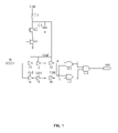
FIG. 1 is a diagram illustrating a circuit to limit circuit delay dependence on voltage;
FIG. 2 is a diagram illustrating one embodiment of the simulated circuit;
FIG. 3 is a diagram illustrating the results of simulations to determine delay of the total circuit delay for a high-to-low input transition at various voltages;
FIG. 4 is a diagram illustrating results of simulations done to determine delay of the total circuit delay for a low-to-high input transition at various voltages; and
FIG. 5 is a diagram illustrating alternate embodiment using non-inverting inverter delay paths and NOR gates.
DETAILED DESCRIPTION
Reference will now be made in detail to the subject matter disclosed, which is illustrated in the accompanying drawings.
The present disclosure is directed to an apparatus for generating a decreasing delay with increasing input voltage to a predetermined voltage value at which point the delay remains constant. An apparatus may include a circuit comprising a voltage regulator receiving an input voltage and two paths of inverters. At least two paths of inverters may be coupled to an input signal, the input signal may be low voltage (e.g. 0) or high voltage (e.g. 1). A first path may be referenced to a reference voltage while the second path may be referenced to the input voltage. The apparatus may include logic gates for receiving the output of each of the first path of inverters and the output of the second path of inverters to generate a desired output. As the input voltage increases, delay of the apparatus may decrease until the input voltage is approximately the same voltage as the reference voltage, at which the delay may remain constant.
The apparatus for generating a decreasing delay with increasing input voltage may operate with low-to-high and high-to-low input transitions. This apparatus may be suitable for use in critical timing paths in integrated circuits that have minimum delay requirements. Examples of these paths include pulse generators for sense amp set signals and wordline pulse widths in SRAM arrays and some dynamic logic circuits.
Referring to FIG. 1 the circuit may use two delay paths, each path may include a plurality of inverters. A first path may be Path I1-I3 and a second path may be Path I4-I6. Depending on the application and requirements, these paths may contain any number of inverters; however, a first path may include a different number of inverters than the second path. P I4-I6 may be connected to input voltage (Vdd), whereas delay path I1-I3 may be connected to a reference (Vref). In the embodiment shown in FIG. 1, circuit may include a voltage regulator. The voltage regulator may receive an input voltage (Vdd) and produce a reference voltage. The voltage regulator may include two transistors (N1 and N2), a resistor (R1) and a capacitor (C1). The reference voltage may be set to a value of two transistor threshold voltages above ground. Other types of voltage regulators may also be employed. The value of reference voltage and the number of inverters in each path are varied to determine the voltage threshold at which the delay through the circuit is no longer reduced with increasing input voltage. The output of these delay paths may be connected to logic gates, such as NAND gates G1 and G2. The output of NAND gates G1 and G2 may be connected to NAND gate G3. The output of G3 may be the output of the circuit. Referring to FIG. 5, an alternate embodiment of a circuit using non-inverting inverter delay paths and the logic gates may be NOR gates to achieve the desired results is shown.
Referring to FIG. 1, the circuit operates as follows for a 0→1 transition at the input:
  • ‘in’ is initially low. ‘a’ and ‘b’ are both initially high. ‘c’ and ‘d’ are initially low and ‘out’ is initially high. ‘in’ goes high making ‘a’ and ‘b’ go low. Since both ‘a’ and ‘b’ must go low to make ‘c’ and ‘d’ go high, the longer of the two delay paths I1-I3 or I4-I6 determines when ‘out’ goes low.
Referring to FIG. 1, the circuit operates as follows for a 1→0 transition at the input:
  • ‘in’ is initially high. ‘a’ and ‘b’ are both initially low. ‘c’ and ‘c’ are initially high, and ‘out’ is initially low. ‘in’ goes low making ‘a’ and ‘b’ go high and ‘c’ and ‘d’ go low. Since both ‘c’ and ‘d’ must go low to make the ‘out’ go high the longer of the two delay paths I1-I3 or I4-I6 determines when ‘out’ goes low.
Circuit variables may include reference voltage and the number of inverters in each path. Referring to FIG. 2, the number of inverters of each path may be varied to achieve a desired result. These variables determine the voltage threshold at which the circuit delay no longer reduces with increasing input voltage.
It is to be understood that both the foregoing general description and the following detailed description are exemplary and explanatory only and are not necessarily restrictive of the present disclosure. The accompanying drawings, which are incorporated in and constitute a part of the specification, illustrate subject matter of the disclosure. Together, the descriptions and the drawings serve to explain the principles of the disclosure.
In the present disclosure, the methods disclosed may be implemented as sets of instructions or software readable by a device. Further, it is understood that the specific order or hierarchy of steps in the methods disclosed are examples of exemplary approaches. Based upon design preferences, it is understood that the specific order or hierarchy of steps in the method can be rearranged while remaining within the disclosed subject matter. The accompanying method claims present elements of the various steps in a sample order, and are not necessarily meant to be limited to the specific order or hierarchy presented.
It is believed that the present disclosure and many of its attendant advantages will be understood by the foregoing description, and it will be apparent that various changes may be made in the form, construction and arrangement of the components without departing from the disclosed subject matter or without sacrificing all of its material advantages. The form described is merely explanatory, and it is the intention of the following claims to encompass and include such changes.

Claims (1)

1. An apparatus, comprising:
a voltage regulator, said voltage regulator receiving an input voltage and producing a reference voltage;
a first path of inverters, said first path of inverters including a first number of inverters, each inverter of said first path of inverters being coupled to said reference voltage, a first inverter of said first path of inverters being coupled to an input;
a second path of inverters, said second path of inverters including a second number of inverters, said second number of inverters being greater than said first number of inverters, each inverter of said second path of inverters being coupled to said input voltage, a first inverter of said second path of inverters being coupled to said input; and
at least one logic gate receiving an output of said first path of inverters and an output of said second path of inverters to produce an output based upon a value of said input,
wherein said apparatus generates a delay that decreases as said input voltage is increased until said input voltage reaches a predetermined voltage, said delay remaining approximately constant when said input voltage is greater than said predetermined voltage.
US12/138,564 2008-06-13 2008-06-13 Method and apparatus to limit circuit delay dependence on voltage Expired - Fee Related US7714630B2 (en)

Priority Applications (1)

Application Number Priority Date Filing Date Title
US12/138,564 US7714630B2 (en) 2008-06-13 2008-06-13 Method and apparatus to limit circuit delay dependence on voltage

Applications Claiming Priority (1)

Application Number Priority Date Filing Date Title
US12/138,564 US7714630B2 (en) 2008-06-13 2008-06-13 Method and apparatus to limit circuit delay dependence on voltage

Publications (2)

Publication Number Publication Date
US20090309644A1 US20090309644A1 (en) 2009-12-17
US7714630B2 true US7714630B2 (en) 2010-05-11

Family

ID=41414184

Family Applications (1)

Application Number Title Priority Date Filing Date
US12/138,564 Expired - Fee Related US7714630B2 (en) 2008-06-13 2008-06-13 Method and apparatus to limit circuit delay dependence on voltage

Country Status (1)

Country Link
US (1) US7714630B2 (en)

Cited By (1)

* Cited by examiner, † Cited by third party
Publication number Priority date Publication date Assignee Title
US20110109366A1 (en) * 2009-11-06 2011-05-12 International Business Machines Corporation Method and Apparatus to Limit Circuit Delay Dependence on Voltage for Single Phase Transition

Families Citing this family (1)

* Cited by examiner, † Cited by third party
Publication number Priority date Publication date Assignee Title
US20220190703A1 (en) * 2019-05-24 2022-06-16 Power Integrations, Inc. Switching delay for communication

Citations (4)

* Cited by examiner, † Cited by third party
Publication number Priority date Publication date Assignee Title
US5459423A (en) 1992-06-18 1995-10-17 Kabushiki Kaisha Toshiba Semiconductor integrated circuit for a stable constant delay time
US6130567A (en) 1997-04-18 2000-10-10 Nec Corporation Semiconductor delay circuit having inverter circuits and transfer gates
US6333652B1 (en) * 1999-05-27 2001-12-25 Rohm Co. Ltd. Delay circuit
US20010054925A1 (en) * 1999-10-22 2001-12-27 Velio Communications, Inc. Low-power low-jitter variable delay timing circuit

Patent Citations (4)

* Cited by examiner, † Cited by third party
Publication number Priority date Publication date Assignee Title
US5459423A (en) 1992-06-18 1995-10-17 Kabushiki Kaisha Toshiba Semiconductor integrated circuit for a stable constant delay time
US6130567A (en) 1997-04-18 2000-10-10 Nec Corporation Semiconductor delay circuit having inverter circuits and transfer gates
US6333652B1 (en) * 1999-05-27 2001-12-25 Rohm Co. Ltd. Delay circuit
US20010054925A1 (en) * 1999-10-22 2001-12-27 Velio Communications, Inc. Low-power low-jitter variable delay timing circuit

Cited By (2)

* Cited by examiner, † Cited by third party
Publication number Priority date Publication date Assignee Title
US20110109366A1 (en) * 2009-11-06 2011-05-12 International Business Machines Corporation Method and Apparatus to Limit Circuit Delay Dependence on Voltage for Single Phase Transition
US8344782B2 (en) * 2009-11-06 2013-01-01 International Business Machines Corporation Method and apparatus to limit circuit delay dependence on voltage for single phase transition

Also Published As

Publication number Publication date
US20090309644A1 (en) 2009-12-17

Similar Documents

Publication Publication Date Title
US7332937B2 (en) Dynamic logic with adaptive keeper
US8680901B2 (en) Power on reset generation circuits in integrated circuits
CN105471409B (en) Low area flip-flop with shared inverter
KR20010049227A (en) Level adjustment circuit and data output circuit thereof
US9853019B2 (en) Integrated circuit device body bias circuits and methods
US8766675B1 (en) Overvoltage protection circuit
US7233178B2 (en) Power-on solution to avoid crowbar current for multiple power supplies' inputs/outputs
Hosseini et al. An energy-efficient level shifter for low-power applications
US9385718B1 (en) Input-output buffer circuit with a gate bias generator
US10114068B1 (en) Methods and apparatus for monitoring aging effects on an integrated circuit
US8653861B2 (en) Control voltage generating circuit, constant current source circuit, and delay circuit and logic circuit including the same
US20140049300A1 (en) Power-on reset circuit
KR101675561B1 (en) Power device
US7714630B2 (en) Method and apparatus to limit circuit delay dependence on voltage
US6753707B2 (en) Delay circuit and semiconductor device using the same
US9557788B2 (en) Semiconductor memory device including array e-fuse
US9984734B2 (en) Programmable integrated circuits with in-operation reconfiguration capability
US20190147956A1 (en) Block decoder of nonvolatile memory and level shifter
US7755407B2 (en) Variable delay circuit, testing apparatus, and electronic device
US9537474B2 (en) Transforming a phase-locked-loop generated chip clock signal to a local clock signal
US20060132187A1 (en) Body biasing for dynamic circuit
US8994415B1 (en) Multiple VDD clock buffer
US8344782B2 (en) Method and apparatus to limit circuit delay dependence on voltage for single phase transition
US9553581B2 (en) Package-aware state-based leakage power reduction
US8988153B1 (en) Ring oscillator with NMOS or PMOS variation insensitivity

Legal Events

Date Code Title Description
AS Assignment

Owner name: INTERNATIONAL BUSINESS MACHINES CORPORATION,NEW YO

Free format text: ASSIGNMENT OF ASSIGNORS INTEREST;ASSIGNORS:BEHRENDS, DERICK G.;CHRISTENSEN, TODD A.;HEBIG, TRAVIS R.;AND OTHERS;REEL/FRAME:021092/0318

Effective date: 20080609

Owner name: INTERNATIONAL BUSINESS MACHINES CORPORATION, NEW Y

Free format text: ASSIGNMENT OF ASSIGNORS INTEREST;ASSIGNORS:BEHRENDS, DERICK G.;CHRISTENSEN, TODD A.;HEBIG, TRAVIS R.;AND OTHERS;REEL/FRAME:021092/0318

Effective date: 20080609

FEPP Fee payment procedure

Free format text: PAYER NUMBER DE-ASSIGNED (ORIGINAL EVENT CODE: RMPN); ENTITY STATUS OF PATENT OWNER: LARGE ENTITY

Free format text: PAYOR NUMBER ASSIGNED (ORIGINAL EVENT CODE: ASPN); ENTITY STATUS OF PATENT OWNER: LARGE ENTITY

REMI Maintenance fee reminder mailed
LAPS Lapse for failure to pay maintenance fees
STCH Information on status: patent discontinuation

Free format text: PATENT EXPIRED DUE TO NONPAYMENT OF MAINTENANCE FEES UNDER 37 CFR 1.362

FP Lapsed due to failure to pay maintenance fee

Effective date: 20140511