US7722242B2 - Lamp fixing structure and backlight module - Google Patents
Lamp fixing structure and backlight module Download PDFInfo
- Publication number
- US7722242B2 US7722242B2 US11/846,155 US84615507A US7722242B2 US 7722242 B2 US7722242 B2 US 7722242B2 US 84615507 A US84615507 A US 84615507A US 7722242 B2 US7722242 B2 US 7722242B2
- Authority
- US
- United States
- Prior art keywords
- lamp
- protecting member
- wire
- hole
- backlight module
- Prior art date
- Legal status (The legal status is an assumption and is not a legal conclusion. Google has not performed a legal analysis and makes no representation as to the accuracy of the status listed.)
- Active, expires
Links
Images


Classifications
-
- F—MECHANICAL ENGINEERING; LIGHTING; HEATING; WEAPONS; BLASTING
- F21—LIGHTING
- F21V—FUNCTIONAL FEATURES OR DETAILS OF LIGHTING DEVICES OR SYSTEMS THEREOF; STRUCTURAL COMBINATIONS OF LIGHTING DEVICES WITH OTHER ARTICLES, NOT OTHERWISE PROVIDED FOR
- F21V19/00—Fastening of light sources or lamp holders
- F21V19/0075—Fastening of light sources or lamp holders of tubular light sources, e.g. ring-shaped fluorescent light sources
- F21V19/008—Fastening of light sources or lamp holders of tubular light sources, e.g. ring-shaped fluorescent light sources of straight tubular light sources, e.g. straight fluorescent tubes, soffit lamps
-
- G—PHYSICS
- G02—OPTICS
- G02F—OPTICAL DEVICES OR ARRANGEMENTS FOR THE CONTROL OF LIGHT BY MODIFICATION OF THE OPTICAL PROPERTIES OF THE MEDIA OF THE ELEMENTS INVOLVED THEREIN; NON-LINEAR OPTICS; FREQUENCY-CHANGING OF LIGHT; OPTICAL LOGIC ELEMENTS; OPTICAL ANALOGUE/DIGITAL CONVERTERS
- G02F1/00—Devices or arrangements for the control of the intensity, colour, phase, polarisation or direction of light arriving from an independent light source, e.g. switching, gating or modulating; Non-linear optics
- G02F1/01—Devices or arrangements for the control of the intensity, colour, phase, polarisation or direction of light arriving from an independent light source, e.g. switching, gating or modulating; Non-linear optics for the control of the intensity, phase, polarisation or colour
- G02F1/13—Devices or arrangements for the control of the intensity, colour, phase, polarisation or direction of light arriving from an independent light source, e.g. switching, gating or modulating; Non-linear optics for the control of the intensity, phase, polarisation or colour based on liquid crystals, e.g. single liquid crystal display cells
- G02F1/133—Constructional arrangements; Operation of liquid crystal cells; Circuit arrangements
- G02F1/1333—Constructional arrangements; Manufacturing methods
- G02F1/1335—Structural association of cells with optical devices, e.g. polarisers or reflectors
- G02F1/1336—Illuminating devices
- G02F1/133602—Direct backlight
- G02F1/133604—Direct backlight with lamps
-
- G—PHYSICS
- G02—OPTICS
- G02F—OPTICAL DEVICES OR ARRANGEMENTS FOR THE CONTROL OF LIGHT BY MODIFICATION OF THE OPTICAL PROPERTIES OF THE MEDIA OF THE ELEMENTS INVOLVED THEREIN; NON-LINEAR OPTICS; FREQUENCY-CHANGING OF LIGHT; OPTICAL LOGIC ELEMENTS; OPTICAL ANALOGUE/DIGITAL CONVERTERS
- G02F1/00—Devices or arrangements for the control of the intensity, colour, phase, polarisation or direction of light arriving from an independent light source, e.g. switching, gating or modulating; Non-linear optics
- G02F1/01—Devices or arrangements for the control of the intensity, colour, phase, polarisation or direction of light arriving from an independent light source, e.g. switching, gating or modulating; Non-linear optics for the control of the intensity, phase, polarisation or colour
- G02F1/13—Devices or arrangements for the control of the intensity, colour, phase, polarisation or direction of light arriving from an independent light source, e.g. switching, gating or modulating; Non-linear optics for the control of the intensity, phase, polarisation or colour based on liquid crystals, e.g. single liquid crystal display cells
- G02F1/133—Constructional arrangements; Operation of liquid crystal cells; Circuit arrangements
- G02F1/1333—Constructional arrangements; Manufacturing methods
- G02F1/1335—Structural association of cells with optical devices, e.g. polarisers or reflectors
- G02F1/1336—Illuminating devices
- G02F1/133602—Direct backlight
- G02F1/133608—Direct backlight including particular frames or supporting means
-
- H—ELECTRICITY
- H01—ELECTRIC ELEMENTS
- H01R—ELECTRICALLY-CONDUCTIVE CONNECTIONS; STRUCTURAL ASSOCIATIONS OF A PLURALITY OF MUTUALLY-INSULATED ELECTRICAL CONNECTING ELEMENTS; COUPLING DEVICES; CURRENT COLLECTORS
- H01R13/00—Details of coupling devices of the kinds covered by groups H01R12/70 or H01R24/00 - H01R33/00
- H01R13/02—Contact members
- H01R13/193—Means for increasing contact pressure at the end of engagement of coupling part, e.g. zero insertion force or no friction
-
- H—ELECTRICITY
- H01—ELECTRIC ELEMENTS
- H01R—ELECTRICALLY-CONDUCTIVE CONNECTIONS; STRUCTURAL ASSOCIATIONS OF A PLURALITY OF MUTUALLY-INSULATED ELECTRICAL CONNECTING ELEMENTS; COUPLING DEVICES; CURRENT COLLECTORS
- H01R33/00—Coupling devices specially adapted for supporting apparatus and having one part acting as a holder providing support and electrical connection via a counterpart which is structurally associated with the apparatus, e.g. lamp holders; Separate parts thereof
- H01R33/05—Two-pole devices
- H01R33/06—Two-pole devices with two current-carrying pins, blades or analogous contacts, having their axes parallel to each other
- H01R33/08—Two-pole devices with two current-carrying pins, blades or analogous contacts, having their axes parallel to each other for supporting tubular fluorescent lamp
- H01R33/0836—Two-pole devices with two current-carrying pins, blades or analogous contacts, having their axes parallel to each other for supporting tubular fluorescent lamp characterised by the lamp holding means
-
- H—ELECTRICITY
- H01—ELECTRIC ELEMENTS
- H01R—ELECTRICALLY-CONDUCTIVE CONNECTIONS; STRUCTURAL ASSOCIATIONS OF A PLURALITY OF MUTUALLY-INSULATED ELECTRICAL CONNECTING ELEMENTS; COUPLING DEVICES; CURRENT COLLECTORS
- H01R13/00—Details of coupling devices of the kinds covered by groups H01R12/70 or H01R24/00 - H01R33/00
- H01R13/02—Contact members
- H01R13/025—Contact members formed by the conductors of a cable end
Definitions
- the invention relates to a fixing structure, a backlight module and a liquid crystal display (LCD) apparatus. More particularly, the invention relates to a lamp fixing structure capable of fixing/interconnecting a wire, a backlight module and an LCD apparatus including the lamp fixing structure.
- LCD liquid crystal display
- a liquid crystal display (LCD) apparatus has been widely used in various electronic products and gradually replaced the conventional cathode ray tube (CRT) display apparatus because the LCD apparatus advantageously has the low power consumption, low generated heat, light weight and non-radiative property.
- LCD liquid crystal display
- the LCD apparatus mainly includes an LCD panel and a backlight module.
- the LCD panel mainly has two substrates and one liquid crystal layer interposed between the two substrates.
- the backlight module is arranged to uniformly distribute light from a light source over the LCD panel.
- FIG. 1 is a schematic illustration showing a conventional backlight module, which is a direct type backlight module 1 .
- the backlight module 1 includes a backplate 11 , a plurality of lamps 12 , two lamp holders 13 , a plurality of lamp protecting members 14 , a plurality of optical films 15 and a frame body 16 .
- the lamps 12 are cold cathode fluorescent lamps (CCFLs) and are separately arranged on the backplate 11 . Two ends of the lamp 12 pass through the lamp protecting member 14 . A wire 121 passes through the lamp protecting member 14 via a small hole of the lamp protecting member 14 , and is electrically connected to the electrode of the lamp 12 by way of hook-soldering.
- the lamp holders 13 arranged to press the lamp protecting members 14 onto the backplate 11 , and the lamp holders 13 are disposed on two lateral sides of the backplate 11 .
- the optical films 15 are disposed on the lamp holders 13 and over the backplate 11 and then combined with the backplate 11 through the frame body 16 so that the lamps 12 and the optical films 15 are fixed between the frame body 16 and the backplate 11 .
- FIG. 2 is a partially schematic illustration showing a dashed-line portion of the backlight module 1 of FIG. 1 .
- the lamp protecting member 14 is disposed in a hollow chamber 131 of the lamp holder 13 .
- An electrode 122 of the lamp 12 is electrically connected to the wire 121 by way of hook-soldering.
- the lamp 12 is inserted into the lamp protecting member 14 .
- the wire 121 passes through a small hole 141 of the lamp protecting member 14 . Because the lamp 12 is connected to the wire 121 , both of the lamp 12 and the wire 121 are inserted into the lamp protecting member 14 through a slit (not shown) of the lamp protecting member 14 .
- the lamp 12 is connected to the wire 121 by way of soldering, the solder between the wire 121 and the lamp 12 may crack (i.e., undergo so called solder crack) due to the human carelessness or the application of improper external force when the operator is assembling or transporting the backlight module 1 .
- the signal cannot be transferred to the lamp 12 through the wire 121 and accordingly the lamp 12 cannot illuminate.
- the structural design of the lamp protecting member 14 is disadvantageous to the soldering operator who is conducting the hook-soldering process directly in the lamp protecting member 14 .
- the operator has to first execute the hook-soldering process and then insert the lamp 12 and the wire 121 , which are connected together, into the lamp protecting member 14 through the slit of the lamp protecting member 14 .
- the diameter of the lamp 12 is larger than the width of the slit, so the connected parts tends to be damaged when the lamp 12 and the wire 121 are being inserted.
- the wire 121 can be wound around the circumference of the lamp protecting member 14 in accordance with another know technique.
- the wire 121 is tightly attached to the lamp protecting member 14 by a relatively complicated manual winding process so that the solder crack does not easily occur under the twitching due to the application of an external force.
- this method greatly increases the production time, and increases production cost undesirably.
- the invention is to provide a lamp fixing structure, which may be conveniently bonded and effectively fix a wire, and a backlight module of an LCD apparatus.
- the invention discloses a lamp fixing structure that is arranged with a lamp, which has an electrode and a wire electrically connected to the electrode.
- the lamp fixing structure includes a lamp holder and at least one lamp protecting member.
- the lamp holder has at least one pressing part.
- the lamp protecting member has a first hole, so that the lamp is inserted into the lamp protecting member.
- the wire passes through the lamp protecting member from the first hole.
- the pressing part presses the lamp protecting member so that the first hole and the wire are fitted tightly.
- the invention further discloses a backlight module, which includes a backplate, a lamp and a lamp fixing structure.
- the lamp has an electrode and a wire electrically connected to the electrode.
- the lamp fixing structure which is disposed on the backplate, has a lamp holder and at least one lamp protecting member.
- the lamp holder has at least one pressing part.
- the lamp protecting member has a first hole, and the lamp is inserted into the lamp protecting member.
- the wire passes through the lamp protecting member from the first hole.
- the pressing part presses the lamp protecting member so that the first hole and the wire are fitted tightly.
- the invention also discloses a liquid crystal display (LCD) apparatus, which includes a backlight module and an LCD panel.
- the backlight module has a backplate, a lamp and a lamp fixing structure.
- the lamp has an electrode and a wire electrically connected to the electrode.
- the lamp fixing structure is disposed on the backplate.
- the lamp fixing structure has a lamp holder and at least one lamp protecting member.
- the lamp holder has at least one pressing part.
- the lamp protecting member has a first hole, and the lamp is inserted into the lamp protecting member.
- the wire passes through the lamp protecting member from the first hole.
- the pressing part presses the lamp protecting member so that the first hole and the wire are fitted tightly.
- the LCD panel is disposed adjacent to the backlight module.
- the lamp fixing structure and the backlight module of the invention have the following advantages. Because the lamp holder has a pressing part, the lamp protecting member has a first hole and the wire passes through the first hole, the pressing part presses the lamp protecting member when the lamp protecting member is disposed in the lamp holder so that the first hole shrinks, and the first hole is fitted tightly to the wire to fix the wire in place. Consequently, it is possible to prevent the solder crack caused by an external force which is applied to the wire.
- a chamber may be formed on a top surface of the lamp protecting member in this invention in order to facilitate the bonding of the wire to the electrode of the lamp and thus the electrical connection of the wire to the electrode of the lamp.
- the invention can achieve the object of fixing the wire using the simple structure design without the need for a complicated manual wire winding process. Thus, the labor and manufacturing costs can be reduced, and the production time can be shortened.
- FIG. 1 is a schematic illustration showing a conventional backlight module
- FIG. 2 is a partially schematic illustration showing the conventional backlight module
- FIG. 3 is a schematic illustration showing a lamp fixing structure according to a first embodiment of the invention.
- FIG. 4 is a schematic illustration showing a lamp protecting member according to a second embodiment of the invention.
- FIG. 5 is a schematic illustration showing a lamp and the lamp protecting member, which are assembled together, according to the a third embodiment of the invention.
- FIG. 6A is a sectional illustration showing the lamp fixing structure before being assembled according to an embodiment of the invention.
- FIG. 6B is a schematic illustration showing the lamp fixing structure after being assembled according to the above mentioned embodiment of the invention.
- FIG. 7 is a schematic illustration showing a backlight module according to another embodiment of the invention.
- FIG. 8 is a schematic illustration showing an LCD apparatus according to still further embodiment of the invention.
- a lamp fixing structure 2 applied with a lamp 20 includes a lamp holder 21 and at least one lamp protecting member 22 .
- the lamp holder 21 has at least one hollow chamber 211 and at least one pressing part 212 , which projects from an inner wall 213 of the lamp holder 21 , and is disposed within the hollow chamber 211 .
- the pressing part 212 is a rib which is integrally (or unitarily) formed with the lamp holder 21 .
- the shape of the pressing part 212 is not particularly limited to that of the rib, but may be any other convenient shape.
- the lamp holder 21 shown in FIG. 3 may be regarded as one portion of the lamp holder 21 of this embodiment.
- the length of the lamp holder 21 may be designed according to the number of the lamps 20 applied therewith.
- the lamp 20 of this embodiment is a cold cathode fluorescent lamp (CCFL) and has an electrode 201 and a wire 202 .
- CCFL cold cathode fluorescent lamp
- the lamp protecting member 22 has a top surface 221 , a slit 222 , a first hole 223 and a protrusion 224 .
- the slit 222 extends from the top surface 221 and is connected to the first hole 223 .
- the protrusion 224 is disposed on the top surface 221 and adjacent to the slit 222 .
- the protrusion 224 has a triangular shape, for example, and is disposed on two sides of the slit 222 . It is to be noted that the protrusion 224 is not restricted to the triangular shape but may have any other shape, and may be disposed on only one side of the slit 222 .
- the lamp protecting member 22 further has a chamber 225 , which is disposed on the top surface 221 and communicates with the first hole 223 , and a second hole 226 , which communicates with the chamber 225 .
- the lamp protecting member 22 of this embodiment may be one entity or have other aspects.
- another lamp protecting member 22 ′ is composed of a plurality of lamp protecting members 22 connected together to form an entity.
- the lamp protecting members 22 are integrally formed.
- at least one reinforcement part 221 ′ may be disposed between the lamp protecting members 22 to reinforce the overall structure intensity.
- another slit 222 ′ still can be formed on the top surface 221 of each lamp protecting member 22 .
- the slit 222 ′ makes the lamp protecting members 22 and 22 ′ be conveniently de-molded after the injection molding because a mold assistant may be placed in the slit 222 ′ when the injection molding is being conducted.
- the lamp 20 passes through and is inserted into the lamp protecting member 22 via the second hole 226 so that one end of the lamp 20 is accommodated within the chamber 225 .
- the wire 202 passes through the lamp protecting member 22 via the first hole 223 .
- the soldering operator connects the wire 202 to the electrode 201 of the lamp 20 in the chamber 225 by way of hook-soldering.
- the chamber 225 allows the soldering operator at the upside to perform the soldering process in the chamber 225 so as to eliminate various problems induced in the prior art, in which the lamp 20 and the wire 202 cannot be inserted into the lamp protecting member 22 until they are bonded together.
- the lamp protecting member 22 may be made of an elastic material, such as rubber, for protecting the lamp 20 and the wire 202 from being rubbed and damaged.
- FIG. 5 is a schematic illustration showing the lamp 20 and the wire 202 , which are bonded.
- the lamp 20 is inserted into the lamp protecting member 22 , and its wire 202 passes through the lamp protecting member 22 from the first hole 223 .
- the lamp protecting member 22 may further have a third hole 227 , through which the wire 202 passes so that the wire 202 passes through the lamp protecting member 22 and is connected to a terminal of a drive control circuit of the lamp 20 and the wire 202 may be fixed to the lamp protecting member 22 more stably.
- FIGS. 6A and 6B are schematically illustrations showing the lamp protecting member 22 and the lamp holder 21 , wherein FIG. 6A shows the state before being assembled and FIG. 6B shows the state after being assembled.
- the lamp protecting member 22 is disposed in the hollow chamber 211 of the lamp holder 21 and is connected to the lamp holder 21 .
- the lamp protecting member 22 may be inserted into or adhered to the lamp holder 21 , or may be limited by an external spatial limiting element, which fixes the relative position between the lamp protecting member 22 and the lamp holder 21 . After the lamp protecting member 22 and the lamp holder 21 are assembled together (see FIG.
- the pressing part 212 of the lamp holder 21 presses the protrusion 224 of the lamp protecting member 22 and the protrusion 224 deforms and presses downward so that the slit 222 and the first hole 223 shrink and the first hole 223 is fitted tightly to the wire 202 to achieve the object of fixing the wire 202 .
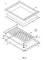
- the backlight module 3 of this embodiment includes a backplate 31 , lamps 20 and lamp fixing structures 2 .
- the lamp fixing structure 2 has been described in the above-mentioned embodiment, so detailed descriptions thereof will be omitted.
- two ends of the lamp 20 are respectively inserted into the lamp protecting members 22 , which are disposed in the lamp holder 21 .
- the wire 202 is fixed in the lamp protecting member 22 .
- the connection relationships between the lamps 20 , the lamp protecting members 22 and the lamp holders 21 have been described in the above-mentioned embodiment, so detailed descriptions thereof will be omitted.
- the lamps 20 and the lamp fixing structures 2 are disposed on the backplate 31 .
- the lamps 20 are disposed on the backplate 31 in parallel, and the lamp holders 21 are disposed on two lateral sides of the backplate 31 .
- the backlight module 3 further has an optical film set 32 and a frame body 33 .
- the optical film set 32 is disposed on the lamp holder 21 and over the backplate 31 and is then combined with the backplate 31 through the frame body 33 so that the lamps 20 , the lamp fixing structure 2 and the optical film set 32 are fixed between the frame body 33 and the backplate 31 . Therefore, the frame body 33 and the backplate 31 may serve as external spatial limiting elements for the lamp protecting member 22 and the lamp holder 21 .
- the optical film set 32 may be selected from at least one of the group consisting of an upper diffuser film, a brightness enhancement film, a prism and a lower diffuser film.
- the frame body 33 , the lamp holder 21 and the backplate 31 may be combined together by way of engaging, adhering or screwing.
- the light rays outputted from the lamps 20 pass through the optical film set 32 and emit out of the backlight module 3 .
- the diffuser film, the brightness enhancement film, the prism or the combination thereof makes the light rays outputted from the lamps 20 be uniformly dispersed, gathered and brightness-enhanced so that the better optical property can be obtained.
- a reflector 34 may be disposed on the backplate 31 so that a portion of the light rays outputted from the lamps 20 can be reflected by the reflector 34 to the optical film set 32 , and the light ray availability and the brightness of the backlight module 3 may be enhanced.
- the LCD apparatus 4 includes a backlight module 3 and an LCD panel 41 .
- the backlight module 3 has been described in the above-mentioned embodiment, so detailed descriptions thereof will be omitted.
- the LCD panel 41 is disposed adjacent to the backlight module 3 .
- the LCD panel 41 includes a first substrate, a second substrate and a liquid crystal layer interposed between the first substrate and the second substrate.
- the LCD panel 41 further has a drive control circuit for controlling displayed frames of the LCD panel 41 .
- the LCD apparatus 4 may further include an external frame 42 , which is combined with the backplate 31 of the backlight module 3 to sandwich the LCD panel 41 between the external frame 42 and the backlight module 3 . At this time, the light rays outputted from the backlight module 3 enter the LCD panel 41 so that the frame is produced.
- the lamp fixing structure and the backlight module of the invention have the following advantages. Because the lamp holder has a pressing part, the lamp protecting member has a first hole and the wire passes through the first hole, the pressing part presses the lamp protecting member when the lamp protecting member is disposed in the lamp holder so that the first hole shrinks, and the first hole is fitted tightly to the wire to fix the wire. Consequently, it is possible to prevent the solder crack caused by the external force for twitching the wire.
- a chamber may be formed on a top surface of the lamp protecting member in this invention in order to facilitate the bonding of the wire to the electrode of the lamp and thus the electrical connection of the wire to the electrode of the lamp.
- the invention can achieve the object of fixing the wire using the simple structure design without the complicated wire. Thus, the labor and manufacturing costs can be reduced, and the production time can be shortened.
Abstract
Description
Claims (6)
Applications Claiming Priority (3)
| Application Number | Priority Date | Filing Date | Title |
|---|---|---|---|
| TW95132247 | 2006-08-31 | ||
| TW095132247A TWI345099B (en) | 2006-08-31 | 2006-08-31 | Lamp fixing structure, backlight module and liquid crystal display apparatus |
| TW95132247A | 2006-08-31 |
Publications (2)
| Publication Number | Publication Date |
|---|---|
| US20080055916A1 US20080055916A1 (en) | 2008-03-06 |
| US7722242B2 true US7722242B2 (en) | 2010-05-25 |
Family
ID=39151237
Family Applications (1)
| Application Number | Title | Priority Date | Filing Date |
|---|---|---|---|
| US11/846,155 Active 2028-02-07 US7722242B2 (en) | 2006-08-31 | 2007-08-28 | Lamp fixing structure and backlight module |
Country Status (2)
| Country | Link |
|---|---|
| US (1) | US7722242B2 (en) |
| TW (1) | TWI345099B (en) |
Cited By (5)
| Publication number | Priority date | Publication date | Assignee | Title |
|---|---|---|---|---|
| US20090051635A1 (en) * | 2007-08-21 | 2009-02-26 | Jung-Hong Park | Liquid crystal display |
| US20090073341A1 (en) * | 2004-04-29 | 2009-03-19 | Dong Im Huo | Liquid crystal module |
| US20100073592A1 (en) * | 2007-04-19 | 2010-03-25 | Kentaro Kamada | Backlight unit and liquid crystal display apparatus |
| US20100171897A1 (en) * | 2009-01-06 | 2010-07-08 | Samsung Electronics Co. Ltd. | Liquid crystal display device |
| US20100321925A1 (en) * | 2009-06-19 | 2010-12-23 | Tatsuji Sudo | Liquid crystal module |
Families Citing this family (4)
| Publication number | Priority date | Publication date | Assignee | Title |
|---|---|---|---|---|
| DE102008036475A1 (en) * | 2008-08-05 | 2010-02-11 | Zumtobel Lighting Gmbh | Device for mounting a lamp socket |
| JP5286422B2 (en) * | 2009-11-06 | 2013-09-11 | シャープ株式会社 | Lighting device, display device, and television receiver |
| JP2011134466A (en) * | 2009-12-22 | 2011-07-07 | Funai Electric Co Ltd | Lamp socket |
| CN102777815B (en) * | 2012-06-12 | 2014-11-12 | 南京中电熊猫液晶显示科技有限公司 | Lateral inlet type backlight module |
Citations (5)
| Publication number | Priority date | Publication date | Assignee | Title |
|---|---|---|---|---|
| US20040008512A1 (en) * | 2002-07-11 | 2004-01-15 | Yong-Il Kim | Backlight assembly and liquid crystal display apparatus having the same |
| US7057678B2 (en) * | 2001-04-17 | 2006-06-06 | Nec Lcd Technologies, Ltd. | Liquid crystal display device having backlight with return substrate above or below a portion of lamp tubes |
| US7137824B2 (en) * | 2003-08-20 | 2006-11-21 | Chi Lin Technology Co., Ltd. | Connecting unit for a backlight module |
| US7452117B2 (en) * | 2005-12-02 | 2008-11-18 | Au Optronics Corp. | Noise reduction device for use in a backlight module |
| US7452102B2 (en) * | 2005-08-08 | 2008-11-18 | Samsung Electronics Co., Ltd. | Lamp holder, lamp assembly having the same, backlight assembly having the same and display device having the same |
-
2006
- 2006-08-31 TW TW095132247A patent/TWI345099B/en not_active IP Right Cessation
-
2007
- 2007-08-28 US US11/846,155 patent/US7722242B2/en active Active
Patent Citations (5)
| Publication number | Priority date | Publication date | Assignee | Title |
|---|---|---|---|---|
| US7057678B2 (en) * | 2001-04-17 | 2006-06-06 | Nec Lcd Technologies, Ltd. | Liquid crystal display device having backlight with return substrate above or below a portion of lamp tubes |
| US20040008512A1 (en) * | 2002-07-11 | 2004-01-15 | Yong-Il Kim | Backlight assembly and liquid crystal display apparatus having the same |
| US7137824B2 (en) * | 2003-08-20 | 2006-11-21 | Chi Lin Technology Co., Ltd. | Connecting unit for a backlight module |
| US7452102B2 (en) * | 2005-08-08 | 2008-11-18 | Samsung Electronics Co., Ltd. | Lamp holder, lamp assembly having the same, backlight assembly having the same and display device having the same |
| US7452117B2 (en) * | 2005-12-02 | 2008-11-18 | Au Optronics Corp. | Noise reduction device for use in a backlight module |
Cited By (9)
| Publication number | Priority date | Publication date | Assignee | Title |
|---|---|---|---|---|
| US20090073341A1 (en) * | 2004-04-29 | 2009-03-19 | Dong Im Huo | Liquid crystal module |
| US7855762B2 (en) * | 2004-04-29 | 2010-12-21 | Lg Display Co., Ltd. | Liquid crystal module |
| US20100073592A1 (en) * | 2007-04-19 | 2010-03-25 | Kentaro Kamada | Backlight unit and liquid crystal display apparatus |
| US20090051635A1 (en) * | 2007-08-21 | 2009-02-26 | Jung-Hong Park | Liquid crystal display |
| US8057065B2 (en) * | 2007-08-21 | 2011-11-15 | Lg Display Co., Ltd. | Liquid crystal display |
| US20100171897A1 (en) * | 2009-01-06 | 2010-07-08 | Samsung Electronics Co. Ltd. | Liquid crystal display device |
| US8310616B2 (en) * | 2009-01-06 | 2012-11-13 | Samsung Display Co., Ltd. | Liquid crystal display device |
| US20100321925A1 (en) * | 2009-06-19 | 2010-12-23 | Tatsuji Sudo | Liquid crystal module |
| US8337042B2 (en) * | 2009-06-19 | 2012-12-25 | Funai Electric Co., Ltd. | Liquid crystal module |
Also Published As
| Publication number | Publication date |
|---|---|
| TW200811525A (en) | 2008-03-01 |
| US20080055916A1 (en) | 2008-03-06 |
| TWI345099B (en) | 2011-07-11 |
Similar Documents
| Publication | Publication Date | Title |
|---|---|---|
| US7722242B2 (en) | Lamp fixing structure and backlight module | |
| US7744265B2 (en) | Backlight assembly without a bottom chassis | |
| US7665879B2 (en) | Light emitting unit and back plate thereof | |
| US20090256796A1 (en) | Display device and method of manufacturing the same | |
| US8013948B2 (en) | Liquid crystal display device having light emitting diode printed circuit board recessed within the bottom cover | |
| KR101165744B1 (en) | Lamp holder, and lamp assembly, back-light and display device having the same | |
| US7651354B2 (en) | Lamp socket, backlight assembly including the lamp socket, and liquid crystal display including the backlight assembly | |
| KR100774581B1 (en) | Lamp holder, back light assembly having the lamp holder and display device having the same | |
| US7980717B2 (en) | Light source assembly and liquid crystal display having the same | |
| JP2007165320A (en) | Lamp fixing member, and backlight assembly and liquid crystal display having same | |
| JP2006351529A (en) | Cold cathode fluorescent tube, its manufacturing method, and backlight assembly and liquid crystal having the same | |
| US8089576B2 (en) | Liquid crystal display module comprising a backlight unit having at least one guide terminal inserted through at least one through hole of the main frame and method of fabricating the same | |
| KR100918280B1 (en) | liquid crystal display device module | |
| KR101751883B1 (en) | Liquid crystal display device including improved flexible printed circuit connecting structure and method the same | |
| KR20070018413A (en) | Backlight assembly and liquid crystal display apparatus having the same | |
| US20060193140A1 (en) | Lamp assembly, backlight assembly and display apparatus having the same | |
| US8049857B2 (en) | Liquid crystal display device | |
| US20130070166A1 (en) | Lighting device, display device and television device | |
| KR20070021590A (en) | Flat fluorescent lamp, backlight assembly and liquid crystal display apparatus having the same | |
| KR20070052390A (en) | Back light assembly and display device having the same | |
| KR20070000855A (en) | Liquid crystal display module which comprises means for preventing light leakage | |
| KR101071134B1 (en) | Liquid crystal display device module | |
| KR20070080276A (en) | Back light assembly and liquid crystal display apparatus having the same | |
| KR20070063665A (en) | Lamp fixing member, back light assembly and liquid crystal display apparatus having the same | |
| US8368820B2 (en) | Lighting device, display device and television receiver |
Legal Events
| Date | Code | Title | Description |
|---|---|---|---|
| AS | Assignment |
Owner name: CHI MEI OPTOELECTRONICS CORP., TAIWAN Free format text: ASSIGNMENT OF ASSIGNORS INTEREST;ASSIGNORS:CHEN, CHENG-HSIANG;HSU, CHIH-HUNG;REEL/FRAME:019757/0153;SIGNING DATES FROM 20070821 TO 20070825 Owner name: CHI MEI OPTOELECTRONICS CORP.,TAIWAN Free format text: ASSIGNMENT OF ASSIGNORS INTEREST;ASSIGNORS:CHEN, CHENG-HSIANG;HSU, CHIH-HUNG;SIGNING DATES FROM 20070821 TO 20070825;REEL/FRAME:019757/0153 |
|
| STCF | Information on status: patent grant |
Free format text: PATENTED CASE |
|
| AS | Assignment |
Owner name: CHIMEI INNOLUX CORPORATION,TAIWAN Free format text: MERGER;ASSIGNOR:CHI MEI OPTOELECTRONICS CORP.;REEL/FRAME:024369/0249 Effective date: 20100318 Owner name: CHIMEI INNOLUX CORPORATION, TAIWAN Free format text: MERGER;ASSIGNOR:CHI MEI OPTOELECTRONICS CORP.;REEL/FRAME:024369/0249 Effective date: 20100318 |
|
| FPAY | Fee payment |
Year of fee payment: 4 |
|
| AS | Assignment |
Owner name: INNOLUX CORPORATION, TAIWAN Free format text: CHANGE OF NAME;ASSIGNOR:CHIMEI INNOLUX CORPORATION;REEL/FRAME:032621/0718 Effective date: 20121219 |
|
| MAFP | Maintenance fee payment |
Free format text: PAYMENT OF MAINTENANCE FEE, 8TH YEAR, LARGE ENTITY (ORIGINAL EVENT CODE: M1552) Year of fee payment: 8 |
|
| MAFP | Maintenance fee payment |
Free format text: PAYMENT OF MAINTENANCE FEE, 12TH YEAR, LARGE ENTITY (ORIGINAL EVENT CODE: M1553); ENTITY STATUS OF PATENT OWNER: LARGE ENTITY Year of fee payment: 12 |