US7744421B2 - Card connector and method of assembling same - Google Patents
Card connector and method of assembling same Download PDFInfo
- Publication number
- US7744421B2 US7744421B2 US12/166,367 US16636708A US7744421B2 US 7744421 B2 US7744421 B2 US 7744421B2 US 16636708 A US16636708 A US 16636708A US 7744421 B2 US7744421 B2 US 7744421B2
- Authority
- US
- United States
- Prior art keywords
- contact
- housing
- card
- arm
- parts
- Prior art date
- Legal status (The legal status is an assumption and is not a legal conclusion. Google has not performed a legal analysis and makes no representation as to the accuracy of the status listed.)
- Expired - Fee Related
Links
Images


Classifications
-
- H—ELECTRICITY
- H01—ELECTRIC ELEMENTS
- H01R—ELECTRICALLY-CONDUCTIVE CONNECTIONS; STRUCTURAL ASSOCIATIONS OF A PLURALITY OF MUTUALLY-INSULATED ELECTRICAL CONNECTING ELEMENTS; COUPLING DEVICES; CURRENT COLLECTORS
- H01R27/00—Coupling parts adapted for co-operation with two or more dissimilar counterparts
- H01R27/02—Coupling parts adapted for co-operation with two or more dissimilar counterparts for simultaneous co-operation with two or more dissimilar counterparts
-
- H—ELECTRICITY
- H01—ELECTRIC ELEMENTS
- H01R—ELECTRICALLY-CONDUCTIVE CONNECTIONS; STRUCTURAL ASSOCIATIONS OF A PLURALITY OF MUTUALLY-INSULATED ELECTRICAL CONNECTING ELEMENTS; COUPLING DEVICES; CURRENT COLLECTORS
- H01R12/00—Structural associations of a plurality of mutually-insulated electrical connecting elements, specially adapted for printed circuits, e.g. printed circuit boards [PCB], flat or ribbon cables, or like generally planar structures, e.g. terminal strips, terminal blocks; Coupling devices specially adapted for printed circuits, flat or ribbon cables, or like generally planar structures; Terminals specially adapted for contact with, or insertion into, printed circuits, flat or ribbon cables, or like generally planar structures
- H01R12/50—Fixed connections
- H01R12/51—Fixed connections for rigid printed circuits or like structures
- H01R12/55—Fixed connections for rigid printed circuits or like structures characterised by the terminals
- H01R12/57—Fixed connections for rigid printed circuits or like structures characterised by the terminals surface mounting terminals
-
- H—ELECTRICITY
- H01—ELECTRIC ELEMENTS
- H01R—ELECTRICALLY-CONDUCTIVE CONNECTIONS; STRUCTURAL ASSOCIATIONS OF A PLURALITY OF MUTUALLY-INSULATED ELECTRICAL CONNECTING ELEMENTS; COUPLING DEVICES; CURRENT COLLECTORS
- H01R12/00—Structural associations of a plurality of mutually-insulated electrical connecting elements, specially adapted for printed circuits, e.g. printed circuit boards [PCB], flat or ribbon cables, or like generally planar structures, e.g. terminal strips, terminal blocks; Coupling devices specially adapted for printed circuits, flat or ribbon cables, or like generally planar structures; Terminals specially adapted for contact with, or insertion into, printed circuits, flat or ribbon cables, or like generally planar structures
- H01R12/70—Coupling devices
- H01R12/71—Coupling devices for rigid printing circuits or like structures
- H01R12/712—Coupling devices for rigid printing circuits or like structures co-operating with the surface of the printed circuit or with a coupling device exclusively provided on the surface of the printed circuit
- H01R12/714—Coupling devices for rigid printing circuits or like structures co-operating with the surface of the printed circuit or with a coupling device exclusively provided on the surface of the printed circuit with contacts abutting directly the printed circuit; Button contacts therefore provided on the printed circuit
-
- H—ELECTRICITY
- H01—ELECTRIC ELEMENTS
- H01R—ELECTRICALLY-CONDUCTIVE CONNECTIONS; STRUCTURAL ASSOCIATIONS OF A PLURALITY OF MUTUALLY-INSULATED ELECTRICAL CONNECTING ELEMENTS; COUPLING DEVICES; CURRENT COLLECTORS
- H01R43/00—Apparatus or processes specially adapted for manufacturing, assembling, maintaining, or repairing of line connectors or current collectors or for joining electric conductors
- H01R43/20—Apparatus or processes specially adapted for manufacturing, assembling, maintaining, or repairing of line connectors or current collectors or for joining electric conductors for assembling or disassembling contact members with insulating base, case or sleeve
- H01R43/24—Assembling by moulding on contact members
Definitions
- the present invention relates generally to card connectors and methods of assembling the same, and particularly to a memory card connector that is incorporated in electronic apparatuses such as digital cameras to allow a memory card to be attached thereto and a method of assembling the memory card connector.
- Electronic apparatuses such as digital cameras, portable audio apparatuses, cellular phones, and electronic copiers have a memory card connector incorporated therein and are used with a memory card having a built-in semiconductor memory device being attached to the memory card connector.
- memory cards such as Memory Stick (trademark), Memory Stick Duo (trademark), SD Memory Card (trademark), and MMC (MultiMedia Card) (trademark).
- memory card connectors have been commercialized that allow selective attachment of any kind of memory card. This type of memory card connector is mounted on a printed circuit board with its lead terminal parts soldered to corresponding pads on the printed circuit board.
- Memory card connectors of this type are divided into those having a single memory card insertion slot common to multiple kinds of memory cards and those having an upper memory card insertion slot and a lower memory card insertion slot.
- the latter memory card connectors have an advantage over the former memory card connectors in that more kinds of memory cards are attachable.
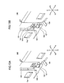
- FIG. 1 is a diagram showing a structure of a conventional memory card connector 1 of the latter type.
- the memory card connector 1 has the structure where an upper housing 5 in which contact members 6 are provided by insert molding is stacked on and fixed to a lower housing 2 in which contact members 3 are provided by insert molding.
- the memory card connector 1 is mounted on a printed circuit board 10 with lead terminal parts 3 a and 6 a thereof being soldered to corresponding pads 10 a and 10 b , respectively, on the printed circuit board 10 . (See, for example, Japanese Laid-Open Patent Application No. 2005-50792.)
- the method of detecting the attachment (attached state) of a memory card to a memory card connector differs depending on the type of the memory card.
- One method is to detect the attachment of a memory card through contact of a predetermined one of the terminals of the memory card with a corresponding contact in the memory card connector.
- the other method is to detect the attachment of a memory card by causing a switch provided in the memory card connector to operate by a side of the memory card pressing the switch.
- the former method is employed for Memory Stick (trademark) and Memory Stick Duo (trademark)
- the latter method is employed for SD Memory Card (trademark) and MMC (MultiMedia Card) (trademark).
- FIGS. 2A and 2B are diagrams for illustrating attachment of a memory card to a conventional memory card connector.
- FIG. 2A shows a conventional memory card connector 1 a without its cover.
- an SD memory card 20 has a knob 23 provided in a recess 22 on an X 2 -side surface 21 thereof to be slidable between a write inhibit (write protect) position P 1 and a write enable position P 2 .
- the memory card connector 1 a to which the SD memory card 20 is attached has an internal switch for detecting the attached SD memory card 20 , which is not graphically illustrated but is usually placed at the bottom (Y 1 ) side of the memory card connector 1 a , and an internal switch 9 for detecting the position of the knob 23 of the attached SD memory card 20 .
- the switch 9 includes a fixed terminal 11 and a movable terminal 12 .
- the movable terminal 12 has a U-shaped part 12 a in the middle and a projection part 12 b at its Y 2 end.
- a foreign object may be sandwiched between the movable terminal and the fixed terminal to cause poor contact.
- the wiping direction is the Y 1 direction perpendicular to the X 2 direction in which the U-shaped part 12 a is pressed, so that the wiping distance is extremely short. Therefore, it is difficult to increase the reliability of the switch 9 , that is, the reliability of the memory card connector 1 a.
- Embodiments of the present invention may solve or reduce one or more of the above-described problems.
- a card connector in which one or more of the above-described problems may be solved or reduced and a method of assembling the same.
- a method of assembling a card connector including a first housing configured to have a first card inserted thereinto to be attached thereto and a second housing configured to have a second card inserted thereinto to be attached thereto, the second housing being provided on the first housing, the method including the steps of combining a plurality of contact members for the second card with the first housing by insert molding, the contact members each having, at a first end, a contact arm part to come into contact with a terminal of the second card, and at a second end, a lead terminal part to be soldered to a pad on a board; bending the contact arm parts of the contact members combined with the first housing by insert molding so that the contact arm parts are parallel to a surface of the first housing facing toward the second housing with ends of the contact arm parts facing a side from which the first card is inserted; and attaching the second housing to the first housing by sliding the second housing on the surface of the first housing from the side from which the first card is inserted so that intermediate portions
- the contact members for the second card is combined with the first housing by insert molding, and the first housing does not include contact members for the second card and is placed on the first housing. Therefore, the vertical positions of the lead terminal parts are not affected by the accuracy of attachment of the second housing onto the first housing. Accordingly, it is possible to increase the accuracy of the vertical positions of the lead terminal parts compared with the structure where a second housing with which contact members for the second card are combined by insert molding is attached onto a first housing. As a result, in the case of mounting the card connector on a printed circuit board, there occurs no mounting failure where some lead terminal parts are out of contact with corresponding pads on the printed circuit board, so that it is possible to mount the card connector onto the printed circuit board with more accuracy.
- a card connector including a housing configured to have a card attached thereto; and a detection switch configured to detect the attachment of the card to the housing, the detection switch including a movable terminal configured to be pressed by the attached card to be elastically bent and a fixed terminal spaced away from and facing the movable terminal, wherein the movable terminal includes an arm part configured to be pressed by the attached card to be elastically bent and a contact part extending from the arm part in a direction in which the arm part is bent, the fixed terminal is shaped to be rubbed by the contact part in response to the bending of the arm part, and the contact part is configured to be displaced in the direction in which the arm part is bent to come into contact with and rub the fixed terminal in response to the bending of the arm part.
- the contact part is displaced in the direction in which the arm part is bent so as to come into contact with and rub the fixed terminal. Therefore, the distance over which the contact part rubs the fixed terminal, that is, the wiping distance, can be significantly longer than it is conventionally, so that it is possible to increase the reliability of the detection switch and accordingly to increase the reliability of the card connector.
- FIG. 1 is a schematic diagram showing a conventional memory card connector having a two-tier structure
- FIGS. 2A and 2B are diagrams for illustrating attachment of a memory card to a conventional memory card connector
- FIG. 3 is a perspective view of a memory card connector and various memory cards attachable thereto according to an embodiment of the present invention
- FIG. 4 is an exploded perspective view of the memory card connector of FIG. 3 according to the embodiment of the present invention.
- FIGS. 7A and 7B are diagrams showing a lower housing module in which the double-contact members before bending are provided by insert molding according to the embodiment of the present invention
- FIG. 8 is a diagram showing the double-contact members to be inserted according to the embodiment of the present invention.
- FIGS. 9A and 9B are diagrams showing the lower housing module where contact arm parts are bent according to the embodiment of the present invention.
- FIG. 11 is a side view showing the upper housing and the lower housing module of FIG. 10 according to the embodiment of the present invention.
- FIG. 12 is a diagram showing the path of the movement of the end of a memory stick in the middle of its insertion according to the embodiment of the present invention.
- FIGS. 13A and 13B are perspective views of a first detection switch of the memory card connector according to the embodiment of the present invention.
- FIGS. 14A and 14B are cross-sectional views of the first detection switch according to the embodiment of the present invention.
- FIG. 15 is a diagram showing a movable terminal member of the first detection switch, a movable terminal member of a second detection switch, and part of a lower housing main body into which part the movable terminal members are incorporated according to the embodiment of the present invention
- FIGS. 16A and 16B are cross-sectional views of a first variation of the first detection switch according to the embodiment of the present invention.
- FIGS. 17A and 17B are cross-sectional views of a second variation of the first detection switch according to the embodiment of the present invention.
- X 1 -X 2 indicates the directions of width
- Y 1 -Y 2 indicates the directions of length
- Z 1 -Z 2 indicates the directions of thickness (height) of a memory card connector or a memory card.
- Y 1 indicates the direction in which the memory card is inserted into the memory card connector
- Y 2 indicates the direction in which the memory card is ejected from the memory card connector.
- FIG. 3 is a perspective view of a memory card connector 60 according to an embodiment of the present invention.
- FIG. 4 is an exploded perspective view of the memory card connector 60 of FIG. 3 .
- FIG. 5 is a cross-sectional view of the memory card connector 60 taken along the line IV-IV of FIG. 3 .
- the memory card connector 60 includes a lower housing module 70 , an upper housing 100 stacked on the upper surface of the lower housing module 70 , and a metal-plate cover member 120 that covers the upper housing 100 .
- the memory card connector 60 has a misinsertion preventing member 130 , a first detection switch 140 , and a second detection switch 160 provided therein.
- the memory card connector 60 has an insertion opening 61 at its Y 2 end.
- the insertion opening 61 includes a lower insertion slot (opening) 62 corresponding to the lower housing module 70 and an upper insertion slot (opening) 63 corresponding to the upper housing 100 .
- the memory card connector 60 is mounted on the printed circuit board 10 with below-described lead terminal parts 81 and 94 being soldered to corresponding pads 10 c and 10 d , respectively, on the printed circuit board 10 .
- the memory card connector 60 is incorporated in an electronic apparatus together with the printed circuit board 10 so that the insertion opening 61 is exposed on the exterior surface of the electronic apparatus.
- the SD memory card 20 , a memory stick 30 , or a multimedia card 40 is selectively attachable to the memory card connector 60 using the lower insertion slot 62 , and a memory stick Duo 50 is attachable to the memory card connector 60 using the upper insertion slot 63 .
- the memory stick 30 and the memory stick Duo 50 have the same terminal arrangement, and the memory stick Duo 50 is three-fifths as long as the memory stick 30 .
- the SD memory card 20 and the multimedia card 40 have substantially the same outside dimensions, substantially the same length as the memory stick Duo 50 , a little larger width than the memory stick 30 , and the same terminal arrangement, but are different in that the SD memory card 20 has the knob 23 .
- the lower housing module 70 is an insert molded component having contact members 80 and double-contact members 90 combined with a lower housing main body 71 of synthetic resin by insert molding.
- a double-contact member refers to a contact member having two contact arm parts.
- movable terminal members 141 and 161 forming the first and second detection switches 140 and 160 are press-fit into and fixed to the lower housing main body 71 . A description is given below of the first and second detection switches 140 and 160 .
- the lower housing main body 71 which has a substantially quadrilateral frame shape, includes an X 1 -side frame rod 72 , an X 2 -side frame rod 73 , and three horizontally laid parts 74 , 75 , and 76 .
- the frame rods 72 and 73 have respective guide grooves 72 a and 73 a on their interior side.
- the center horizontally laid part 75 has projection parts 75 a projecting in the Z 1 direction on its Y 2 -side step part.
- the contact members 80 are inserted in the horizontally laid part 74 positioned close to the lower insertion slot 62 , and are arranged in correspondence to the terminals of each of the SD memory card 20 and the multimedia card 40 .
- the double-contact members 90 are combined with the Y 1 -end horizontally laid part 76 by insert molding.
- FIG. 6 is a perspective view of the double-contact members 90 .
- each double-contact member 90 has a first (shorter) contact arm part 91 , a second (longer) contact arm part 92 longer than the first contact part 91 , and the lead terminal part 94 .
- the contact arm part 91 , the contact arm part 92 , and the lead terminal part 94 are connected at a base 93 of the contact arm part 91 .
- the lead terminal part 94 extends in the Y 1 direction from the base 93 of the contact arm part 91 .
- the contact arm part 91 is combined with the horizontally laid part 76 by insert molding.
- the contact arm parts 91 of the double-contact members 90 are arranged in correspondence to the arrangement of the terminals of the memory stick 30 .
- the contact arm parts 92 are vertically positioned on the Z 1 side relative to the frame rods 72 and 73 to extend in the Y 2 direction, and are arranged in correspondence to the arrangement of the terminals of the memory stick Duo 50 .
- Each contact arm part 92 has an inverse V-shaped contact part 92 a at its Y 2 end and a bulge part 92 b continuing from the contact part 92 a.
- the upper housing which is a molded component of synthetic resin, has a frame shape and includes an X 1 -side frame rod 101 , an X 2 -side frame rod 102 , and two horizontally laid parts 103 and 104 .
- the frame rods 101 and 102 have respective guide grooves 101 a and 102 a on their interior side.
- Multiple through holes 105 are formed in the horizontally laid part 104 . As shown enlarged in FIG. 10 , the through holes 105 correspond to the contact arm parts 92 , and are large enough to allow the corresponding contact arm parts 92 a to penetrate therethrough. Each through hole 105 has a slit part 107 large enough to allow the corresponding bulge part 92 b to be press-fit thereinto, formed at its Z 2 -side end, and has a tapered part 106 formed at its Y 1 -side entrance.
- the cover member 120 has a top plate part 121 , side plate parts 122 and 123 on the X 1 and X 2 sides, respectively, and a Y 1 -side plate part 124 .
- a fixed terminal part 125 of the first detection switch 140 and a fixed terminal part 129 of the second detection switch are formed on the side plate part 123 .
- the misinsertion preventing member 130 has triangular parts 131 and 132 on the X 1 and X 2 sides, respectively, and has shaft parts 133 and 134 projecting from its X 1 and X 2 ends, respectively.
- the memory card connector 60 is assembled through the process of manufacturing the lower housing module 70 , the process of attaching the upper housing 100 , and the process of attaching the cover member 120 .
- the lower housing module 70 is manufactured through the process of insert molding and the bending of the contact arm parts 92 A.
- Suffix A of reference numeral 92 A indicates the state before bending.
- FIGS. 7A and 7B are diagrams showing a lower housing module 70 A in which double-contact members 90 A are provided by insert molding.
- FIG. 8 is a diagram showing the double-contact members 90 A before the contact arm parts 92 A are bent.
- the lower housing module 70 A shown in FIGS. 7A and 7B are manufactured by setting the contact members 80 and the double-contact members 90 A shown in FIG. 8 in a mold; molding the lower housing main body 71 by injecting synthetic resin into the mold; and providing the contact members 80 and the double-contact members 90 A in the horizontally laid part 74 and the horizontally laid part 76 , respectively, by insert molding.
- each double-contact member 90 A has the contact arm part 91 extending in the Y 2 direction on one end side and the lead terminal part 94 extending in the Y 1 direction on the other end side, and the contact arm part 92 A branches off at the base 93 of the contact arm part 91 to extend in the Z 1 direction.
- the contact arm part 91 , the contact arm part 92 A, and the lead terminal part 94 are joined at the base 93 .
- the contact arm part 92 A forms a 90° angle with respect to the contact arm part 91 .
- the lead terminal part 94 which is bent like an L-letter shape, is a terminal to be soldered to the corresponding pad 10 d on the printed circuit board 10 when the memory card connector 60 is mounted on the printed circuit board 10 .
- Each double-contact member 90 A has a portion near the base 93 of the contact arm part 91 provided in (combined with) the horizontally laid part 76 by insert molding.
- the contact arm parts 91 are arranged in correspondence to the arrangement of the terminals of the memory stick 30 .
- the contact arm parts 92 A face the Z 1 direction.
- all the contact members 80 and all the double contact members 90 A are arranged like comb teeth, and are cut to be independent after insert molding.
- the contact arm parts 92 A are bent 90° to face the Y 2 direction, to be the contact arm parts 92 .
- the contact arm parts 92 are vertically positioned on the Z 1 side relative to the frame rods 72 and 73 , and extend in the Y 2 direction.
- the contact arm parts 92 are arranged in correspondence with the arrangement of the terminals of the memory stick Duo 50 .
- Each contact arm part 92 has the inverse V-shaped contact part 92 a at its Y 2 end and the bulge part 92 b continuing from the contact part 92 a.
- the movable terminal members 141 and 161 are press-fit into and fixed to the lower housing main body 71 , and the misinsertion preventing member 130 is attached to the lower housing main body 71 , so that the lower housing module 70 is completed.
- the upper housing 100 is placed on the lower housing main body 71 of the lower housing module 70 at its Y 2 end, and is caused to slide in the Y 1 direction along the upper surface of the lower housing main body 71 .
- the contact parts 92 a are guided by the tapered parts 106 to be smoothly fit into the corresponding though holes 105 , and pass through the through holes 105 to project in the Y 2 direction.
- the bulge parts 92 b are tightly fit into the corresponding slit parts 107 at the Z 2 ends of the through holes 105 .
- Projections 101 b and 102 b of the upper housing 100 are fit into recesses 72 b and 73 b of the frame rods 72 and 73 , respectively, and projections 101 c and 102 c of the upper housing 100 are fit into recesses 72 c and 73 c of the frame rods 72 and 73 , respectively, so that the upper housing 100 is positioned, and is engaged with and fixed to the lower housing module 70 .
- the bulge parts 92 b in the middle of the contact arm parts 92 are fit into and fixed to the corresponding slit parts 107 , and the contact parts 92 a are aligned to correspond to the arrangement of the terminals of the memory stick Duo 50 .
- the contact arm parts 92 are bent at an angle ⁇ , which is several degree less than 90°, that is, at an angle a little shallower than 90°, in consideration of variations in the bending angle as indicated by two-dot chain lines in FIG. 11 .
- the contact arm parts 92 are bent just 90° by pressing a portion 151 ( FIG. 9 ) of the bent contact arm parts 92 (the Y1 side portion of the bulge parts 92 b ) from above using a jig 150 having an end shaped like comb teeth, so that the contact parts 92 a are aligned with accuracy and the contact arm parts 92 are prevented from being buckled at the time of press-fitting.
- the multiple through holes 105 are smoothly fit to the corresponding contact parts 92 a , and the bulge parts 92 b are press-fit into the corresponding slit parts 107 without causing buckling of the contact arm parts 92 .
- the cover member 120 has openings 122 a and 123 a of its side plate parts 122 and 123 fit to corresponding projections 72 d and 73 d , respectively, of the lower housing main body 71 so as to be fixed to and cover the stacked lower housing module 70 and upper housing 100 .
- the memory card connector 60 has the upper housing 100 positioned on the lower housing module 70 with the upper housing 100 being fit to the contact parts 92 a , the projections 101 b and 102 b being fit into the recesses 72 b and 73 b , respectively, and the projections 101 c and 102 c being fit into the recesses 72 c and 73 c , respectively.
- the openings 122 a and 123 a of the side plate parts 122 and 123 being fit to the corresponding projections 72 d and 73 d , respectively, of the lower housing main body 71 , so that the cover member 120 is fixed to and covers the stacked lower housing module 70 and upper housing 100 .
- the misinsertion preventing member 130 is supported between the lower housing main body 71 and the upper housing 100 .
- the lead terminal parts 94 arranged in the X 1 -X 2 directions have good surface accuracy.
- the memory card connector 60 is assembled as described above. As a result, variations (error) in the attachment of the upper housing 100 onto the lower housing module do not affect variations in the vertical positions of the lead terminal parts 94 corresponding to the contact arm parts 92 inside the upper housing 100 , and the vertical positions of the lead terminal parts 94 arranged in the X 1 -X 2 directions relative to the lower surface of the memory card connector 60 are determined with more accuracy than conventionally. Accordingly, as shown in FIG.
- the lead terminal parts 94 come into contact with the corresponding pads 10 d of the printed circuit board 10 and it is ensured that the lead terminal parts 94 are soldered to the corresponding pads 10 d , thereby solving the problem of some lead terminal parts being not soldered to and out of contact with the corresponding pads 10 d of the printed circuit board 10 .
- the lower housing module 70 has an internal space for attachment of the SD memory card 20 , the memory stick 30 , and the multimedia card 40 .
- the upper housing 100 has an internal space for attachment of the memory stick Duo 50 .
- the SD memory card 20 is attached to the memory card connector 60 by having its terminals come into contact with the corresponding contact members 80 .
- the multimedia card 40 is also attached to the memory card connector 60 by having its terminals come into contact with the corresponding contact members 80 .
- the memory stick 30 is attached to the memory card connector 60 by having its terminals come into contact with the corresponding contact arm parts 91 .
- FIG. 12 is a diagram showing the path of the movement of the end of the memory stick 30 in the middle of its insertion.
- the memory stick 30 is inserted into the corresponding space inside the lower housing module 70 to pass over the upper side of the contact members 80 to reach the bottom of the space.
- An operator may insert the memory stick 30 into the lower insertion slot 62 with its rear end side lifted in the Z 1 direction.
- the memory stick 30 passes over the upper side of the contact members 80 in an inclined position with its front (leading) end side down as shown in FIG. 12 .
- the end side of the contact members 80 may be excessively bent in the Z 2 direction, so that in some cases, the contact members 80 may have their respective ends plastically deformed in the Z 2 direction.
- the lower housing main body 71 has the projection parts 75 a projecting in the Z 1 direction in a Y 2 -side depressed part of the horizontally laid part 75 , that is, a part corresponding to the ends of the contact members 80 .
- the memory stick 30 is positioned on the projection parts 75 a to be forcibly displaced in the Z 1 direction as indicated by two-dot chain lines in FIG. 12 before the end of the memory stick 30 reaches the ends of the contact members 80 , and moves over the contact members 80 .
- the deformation of the end parts of the contact members 80 in the Z 2 direction is limited so as to prevent plastic deformation of the contact members 80 .
- the memory stick Duo 50 is attached to the memory card connector 60 using the upper insertion slot 63 .
- the memory stick Duo 50 is attached to the memory card connector 60 by having its terminals come into contact with the corresponding contact arm parts 92 .
- the attached memory card itself closes the lower insertion slot 62 to prevent another memory card from being attached through the lower insertion slot 62 .
- the misinsertion preventing member 130 is pressed in the Y 1 direction by the attached memory card to be rotated approximately 90° in the counterclockwise direction in FIG. 5 , so that the triangular parts 131 and 132 ( FIG. 4 ) project into the internal space of the upper housing 100 to prevent the memory stick Duo 50 from being attached to the memory card connector 60 in the upper housing 100 .
- the misinsertion preventing member 130 is held by the attached memory stick Duo 50 , so that the triangular parts 131 and 132 project into the internal space of the lower housing main body 71 to prevent the SD memory card 20 , the memory stick 30 , or the multimedia card 40 from being attached to the memory card connector 60 in the lower housing main body 71 .
- the double-contact members 90 are configured to have the two contact arm parts 91 and 92 . This does not cause any inconvenience or compatibility problems because the memory stick Duo 50 has the same terminal arrangement as the memory stick 30 and is prevented from being attached to the memory card connector 60 when the memory stick 30 is attached thereto.
- the contact members 90 each having the contact arm part 91 , the contact arm part 92 , and the lead terminal part 94 may be replaced with contact members each having the contact arm part 92 and the lead terminal part 94 .
- the memory card connector 60 has the first detection switch 140 and the second detection switch 160 provided therein.
- FIG. 13A and FIG. 14A shows the normal state, that is, the OFF state, of the first detection switch 140 .
- FIG. 13B and FIG. 14B shows the first detection switch 140 turned ON into an operating state.
- FIG. 15 is a diagram showing the movable terminal member 141 of the first detection switch 140 , the movable terminal member 161 of the second detection switch 160 , and part of the lower housing main body 71 to which part the movable terminal members 141 and 161 are press-fit and fixed.
- the upper surface of the frame rod 73 of the lower housing main body 71 is shaped so that the movable terminal member 141 and the movable terminal member 161 are press-fit into and fixed to the frame rod 73 so as to be accommodated.
- the first detection switch 140 detects attachment of the SD memory card 20 or the multimedia card 40 .
- the first detection switch 140 includes the movable terminal member 141 and the fixed terminal part 125 formed by cutting and raising part of the side plate part 123 of the cover member 120 .
- the movable terminal member 141 is shown with the same orientation as the orientation with which the movable terminal member 141 is fixed to the frame rod 73 .
- the movable terminal member 141 which is a component formed of a metal plate by press molding, includes a base 142 ; a bulge part 143 , a lead terminal part, and a long arm part 145 extending in different directions from the base 142 ; and a contact part 146 at the end of the arm part 145 .
- the contact part 146 is shaped like a horseshoe and is three-dimensional.
- the bulge part 143 is bent in the Z 2 direction from the base 142 .
- the lead terminal part 144 has an L-letter shape and extends in the Y 1 direction from the base 142 .
- the base 142 has a part 142 a thereof bent in the Z 1 direction, and the arm part 145 extends in the Y 2 direction from the bent part 142 a .
- the arm part 145 is positioned in the Y-Z plane, and is elastically bendable so that its end is displaced in the X 2 direction.
- the arm part 145 includes a V-shaped end part 145 a projecting in the X 1 direction.
- the contact part 146 includes two symmetrical lead parts 147 and 148 .
- the lead parts 147 and 148 each have a crank shape.
- the lead parts 147 and 148 stem from the arm part 145 in directions perpendicular to the arm part 145 , that is, in the Z 1 and Z 2 directions, to be bent and extend in the X 2 direction.
- the lead parts 147 and 148 form a shape like a horseshoe lying on its side in a view from the Y 2 side ( FIGS. 14A and 14B ).
- the lead parts 147 and 148 stem from the arm part 145 and extend in the X 2 direction, that is, extend in the direction in which the arm part 145 is elastically bendable. Further, referring also to FIG.
- the lead parts 147 and 148 include respective end parts 147 a and 148 a projecting toward each other. Further, the lead parts 147 and 148 are symmetrically inclined at an angle ⁇ to reduce the distance (or narrow the gap) between the end parts 147 a and 148 a .
- the angle ⁇ is approximately 10°.
- the movable terminal member 141 is attached to the frame rod 73 with the bulge part 143 being press-fit into a slit 73 f of the frame rod 73 , thereby having the base 142 fixed to the frame rod 73 .
- the contact part 146 has its end side facing an opening part 73 e formed in the frame rod 73 .
- the contact part 146 is deformable in the X 1 -X 2 directions by the bending of the arm part 145 . That is, the contact part 146 is displaced in the direction in which the end of the arm part 145 is bent.
- the fixed terminal part 125 is formed on the side plate part 123 of the cover member 120 by cutting and raising a part of the side plate part 123 , and has a substantially trapezoidal cross section taken along the X-Z plane.
- the fixed terminal part 125 includes lug parts 126 and 127 each bent in the X 2 direction from the side plate part 123 .
- the Z 1 -side lug part 126 and the Z 2 -side lug part 127 are symmetrically inclined to increase the distance (widen the gap) between their respective end parts when viewed from their base side.
- the lug part 126 and the lug part 127 are inclined outward (away from each other) at an angle ⁇ relative to the direction in which the contact part 146 moves (the X 2 direction)
- the angle ⁇ is approximately 25°. That is, the fixed terminal part 125 is shaped to be rubbed by the end parts 147 a and 148 a of the contact part 146 when the contact part 146 is displaced in the direction in which the end of the arm part 145 is bent.
- ⁇ > ⁇ between ⁇ and ⁇ There is a relationship of ⁇ > ⁇ between ⁇ and ⁇ .
- the contact part 146 faces the fixed terminal part 125 with a space therebetween.
- the SD memory card 20 or the multimedia card 40 When the SD memory card 20 or the multimedia card 40 is inserted into and attached to the memory card connector 60 , the SD memory card 20 or the multimedia card 40 has part of its X 2 -side surface near the end in the insertion direction pressing away the end part 145 a of the arm part 145 in the X 2 direction, so that the arm part 145 is bent in the X 2 direction.
- the contact part 146 is displaced in the X 2 direction to approach the fixed terminal part 125 , so that the end parts 147 a and 148 a come into contact with the lug parts 126 and 127 , respectively, to move in such a manner as to be positioned on the lug parts 126 and 127 while rubbing their surfaces. Consequently, the lead parts 147 and 148 mount the fixed terminal part 125 to be finally in the position as shown in FIG. 14B , when the first detection switch 140 is turned ON.
- the direction in which the contact part 146 is displaced (the X 2 direction) is the same as the direction in which the arm part 145 is bent (the X 2 direction). Therefore, the distance L 10 ( FIG. 14B ) over which the end parts 147 a and 148 b move rubbing the lug parts 126 and 127 , respectively, is several times longer than in the conventional switch. As a result, the wiping effect that removes a foreign object becomes stronger than it is conventionally.
- the lead parts 147 and 148 of the contact part 146 hold the fixed terminal part 125 therebetween. Therefore, even if the contact part 146 is slightly out of alignment with the fixed terminal part 125 in the Z 1 -Z 2 directions in the state shown in FIG. 13A , the position of the contact part 146 is corrected in the process of the contact part 146 coming into contact with the fixed terminal part 125 , so that the end parts 147 a and 148 a stably contact the lug parts 126 and 127 , respectively.
- the second detection switch 160 operates in the same manner as the first detection switch 140 and has a higher reliability than conventionally, so that the memory card connector 60 has a higher reliability than conventionally.
- the first and second detection switches 140 and 160 may be configured so that a single lead part rubs a corresponding lug part of the fixed terminal part ( 125 , 129 ) by omitting one of the paired lead parts.
- the frame rod 73 may be provided with a frame part similar to a frame part 180 shown in FIGS. 17A and 17B so that the contact part 146 is positioned by the frame part when the first detection switch 140 is OFF.
- the wiping direction is perpendicular to a direction in which the arm part is bent
- the arm part is required to have a considerable length in order to increase the wiping distance, so that it is impossible to juxtapose the first and second detection switches.
- the wiping direction is the same as the direction in which the arm part is bent. Accordingly, the lengths L 1 and L 2 ( FIG. 15 ) of the movable terminal members 141 and 161 may be small, so that the first and second detection switches 140 and 160 may be placed side by side on the frame rod 73 .
- the memory card connector 60 is mounted on the printed circuit board 10 of an electronic apparatus with leg parts 122 b and 123 b ( FIG. 3 and FIG. 4 ) of the cover member 120 being screwed to the printed circuit board 10 and soldered to corresponding ground patterns thereof (not graphically illustrated), the lead terminal part 144 of the movable terminal member 141 and the lead terminal part 164 of the movable terminal member 161 being soldered to corresponding pads at the edge of the pattern of a detector circuit (not graphically illustrated) on the printed circuit board 10 , and the lead terminal parts 81 and 94 of the contact members 80 and 90 being soldered to the corresponding pads 10 c and 10 d of the printed circuit board 10 . Accordingly, when the first detection switch 140 or the second detection switch 160 is turned ON, the detector circuit suitably operates to control the electronic apparatus.
- the first detection switch 140 A includes a movable terminal member 141 A and a fixed terminal part 125 A.
- the movable terminal member 141 A includes a contact part 146 A.
- the contact part 146 A includes lead parts 147 A and 148 A.
- the gap between the lead parts 147 A and 148 A narrows toward the ends thereof so that the contact part 146 A has a triangular shape.
- the fixed terminal part 125 A has a horizontal lug part 170 bent in the X 1 direction, that is, bent toward the inside of the memory card connector 60 .
- the frame rod 73 includes a tapered part 171 serving as a positioning part. The tapered part 171 is positioned at the end of the lug 170 .
- end parts 147 Aa and 148 Aa of the lead parts 147 A and 148 A holds the tapered part 171 therebetween so that the contact part 146 A is positioned as shown in FIG. 16A .
- the first detection switch 140 B includes a movable terminal member 141 B and a fixed terminal part 125 B.
- a contact part 146 B of the movable terminal member 141 B is larger than the contact part 146 of the above-described movable terminal member 141 .
- the contact part 146 B includes lead parts 147 B and 148 B that are inclined to narrow their gap toward the end side.
- the fixed terminal part 125 B includes horizontal lug parts 126 B and 127 B.
- the frame rod 73 includes the frame part 180 serving as a positioning part.
- the frame part 180 includes upper and lower horizontally laid parts 181 and 182 serving as a guide part.
- the contact part 146 B When the first detection switch 140 B is OFF, the contact part 146 B has its end side portion fit inside the frame part 180 with the upper surface of the end side portion of the lead part 147 B contacting the upper horizontally laid part 181 and the lower surface of the end side portion of the lead part 148 B contacting the lower horizontally laid part 182 .
- the contact part 146 B is positioned by the frame part 180 , and faces the fixed terminal part 125 B.
- the arm part 145 When the SD memory card 20 or the multimedia card 40 in inserted into and attached to the memory card connector 60 , the arm part 145 is bent in the X 2 direction, so that the contact part 146 B is displaced in the X 2 direction.
- the lead parts 147 B and 148 B are guided by the horizontally laid parts 181 and 182 , respectively, to deform to narrow their gap toward the end side, so that the end parts 147 Ba and 148 Ba move while performing wiping, rubbing the surfaces of the corresponding lug parts 126 B and 127 B, so as to be in the state shown in FIG. 17B .
- the contact part 146 B wipes the surfaces of the fixed terminal part 125 B over a sufficient distance L 12 ( FIG. 17B ).
- the lead parts 147 B and 148 B hold the fixed terminal part 125 B therebetween, so that the first detection switch 140 B is turned ON.
- the detection switches 140 and 160 are applicable to card connectors to which not only memory cards but also a card-like object is attachable.
- a card connector including a first housing configured to have a first card inserted thereinto to be attached thereto; a second housing configured to have a second card inserted thereinto to be attached thereto, the second housing being provided on the first housing; and a plurality of contact members for the second card combined with the first housing by insert molding, the contact members each having, at a first end, a contact arm part to come into contact with a terminal of the second card, and at a second end, a lead terminal part to be soldered to a pad on a board, wherein the contact arm parts are placed inside the second housing with intermediate portions thereof fixed to a part of the second housing.
- a card connector including a first housing configured to have a first card inserted thereinto to be attached thereto; a second housing configured to have a second card inserted thereinto to be attached thereto, the second card having a plurality of terminals arranged in correspondence to an arrangement of terminals of the first card, the second housing being provided on the first housing; a plurality of double-contact members having, at a first end, respective first contact arm parts corresponding to the terminals of the first card and respective second contact arm parts branching off from bases of the first contact arm parts and corresponding to the terminals of the second card, and having, at a second end, respective lead terminal parts to be soldered to corresponding pads on a board, wherein the double-contact members have the bases of the first contact arm parts combined with the first housing by insert molding, and the second contact arm parts are placed inside the second housing with respective intermediate portions thereof fixed to a part of the second housing.
- a method of assembling a card connector including a first housing configured to have a first card inserted thereinto to be attached thereto and a second housing configured to have a second card inserted thereinto to be attached thereto, the second housing being provided on the first housing, the method including the steps of combining a plurality of contact members for the second card with the first housing by insert molding, the contact members each having, at a first end, a contact arm part to come into contact with a terminal of the second card, and at a second end, a lead terminal part to be soldered to a pad on a board; bending the contact arm parts of the contact members combined with the first housing by insert molding so that the contact arm parts are parallel to a surface of the first housing facing toward the second housing with ends of the contact arm parts facing a side from which the first card is inserted; and attaching the second housing to the first housing by sliding the second housing on the surface of the first housing from the side from which the first card is inserted so that intermediate portions
- a method of assembling a card connector including a first housing configured to have a first card inserted thereinto to be attached thereto and a second housing configured to have a second card inserted thereinto to be attached thereto, the second card having a plurality of terminals arranged in correspondence to an arrangement of terminals of the first card, the second housing being provided on the first housing, the method including the steps of combining bases of first contact arm parts of a plurality of double-contact members with the first housing by insert molding, the double-contact members having, at a first end, the respective first contact arm parts corresponding to the terminals of the first card and respective second contact arm parts branching off from the bases of the first contact arm parts and corresponding to the terminals of the second card, and having, at a second end, respective lead terminal parts to be soldered to corresponding pads on a board; bending the second contact arm parts of the double-contact members combined with the first housing by insert molding so that the second contact arm parts are parallel to a surface of
- the contact members for the second card is combined with the first housing by insert molding, and the first housing does not include contact members for the second card and is placed on the first housing. Therefore, the vertical positions of the lead terminal parts are not affected by the accuracy of attachment of the second housing onto the first housing. Accordingly, it is possible to increase the accuracy of the vertical positions of the lead terminal parts compared with the structure where a second housing with which contact members for the second card are combined by insert molding is attached onto a first housing. As a result, in the case of mounting the card connector on a printed circuit board, there occurs no mounting failure where some lead terminal parts are out of contact with corresponding pads on the printed circuit board, so that it is possible to mount the card connector onto the printed circuit board with more accuracy.
- a card connector including a housing configured to have a card attached thereto; and a detection switch configured to detect the attachment of the card to the housing, the detection switch including a movable terminal configured to be pressed by the attached card to be elastically bent; and a fixed terminal spaced away from and facing the movable terminal, wherein the movable terminal includes an arm part configured to be pressed by the attached card to be elastically bent; and a contact part extending from the arm part in a direction in which the arm part is bent, the fixed terminal is shaped so as to be rubbed by the contact part in response to the bending of the arm part, and the contact part is configured to be displaced in the direction in which the arm part is bent so as to come into contact with and rub the fixed terminal in response to the bending of the arm part.
- the contact part is displaced in the direction in which the arm part is bent so as to come into contact with and rub the fixed terminal. Therefore, the distance over which the contact part rubs the fixed terminal, that is, the wiping distance, can be significantly longer than it is conventionally, so that it is possible to increase the reliability of the detection switch and accordingly to increase the reliability of the card connector.
Abstract
Description
Claims (17)
Applications Claiming Priority (4)
| Application Number | Priority Date | Filing Date | Title |
|---|---|---|---|
| JP2007-279949 | 2007-10-29 | ||
| JP2007279949A JP5329792B2 (en) | 2007-10-29 | 2007-10-29 | Card connector |
| JP2007-279950 | 2007-10-29 | ||
| JP2007279950A JP5128235B2 (en) | 2007-10-29 | 2007-10-29 | Card connector |
Publications (2)
| Publication Number | Publication Date |
|---|---|
| US20090111288A1 US20090111288A1 (en) | 2009-04-30 |
| US7744421B2 true US7744421B2 (en) | 2010-06-29 |
Family
ID=40583395
Family Applications (1)
| Application Number | Title | Priority Date | Filing Date |
|---|---|---|---|
| US12/166,367 Expired - Fee Related US7744421B2 (en) | 2007-10-29 | 2008-07-02 | Card connector and method of assembling same |
Country Status (1)
| Country | Link |
|---|---|
| US (1) | US7744421B2 (en) |
Cited By (4)
| Publication number | Priority date | Publication date | Assignee | Title |
|---|---|---|---|---|
| US20100190365A1 (en) * | 2009-01-23 | 2010-07-29 | Ddk Ltd. | Card connector |
| US20140242845A1 (en) * | 2013-02-22 | 2014-08-28 | Fujitsu Limited | Connector |
| US9979113B2 (en) * | 2016-04-08 | 2018-05-22 | Foxconn Interconnect Technology Limited | Electrical connector and assembly thereof |
| US20190089085A1 (en) * | 2017-09-21 | 2019-03-21 | Fanuc Corporation | Connector connecting structure |
Families Citing this family (6)
| Publication number | Priority date | Publication date | Assignee | Title |
|---|---|---|---|---|
| JP2009176510A (en) * | 2008-01-23 | 2009-08-06 | Honda Tsushin Kogyo Co Ltd | Memory card connector |
| JP5286126B2 (en) * | 2009-03-24 | 2013-09-11 | 富士通コンポーネント株式会社 | Card connector |
| JP5476846B2 (en) * | 2009-08-06 | 2014-04-23 | ミツミ電機株式会社 | Connector and detection switch |
| CN103714854B (en) * | 2012-09-28 | 2017-08-25 | 群联电子股份有限公司 | Storage device and preparation method thereof |
| TWI751592B (en) * | 2020-06-24 | 2022-01-01 | 維將科技股份有限公司 | Card connector |
| CN112993624B (en) * | 2021-02-05 | 2022-09-06 | 深圳市豪塑科技有限公司 | Double-position connector and assembling method thereof |
Citations (8)
| Publication number | Priority date | Publication date | Assignee | Title |
|---|---|---|---|---|
| US6120322A (en) * | 1998-08-31 | 2000-09-19 | Hon Hai Precision Ind. Co., Ltd. | Memory card connection device |
| JP2001167844A (en) | 1999-12-09 | 2001-06-22 | Yamaichi Electronics Co Ltd | Card connector |
| US6685512B2 (en) * | 2001-01-19 | 2004-02-03 | Yamaichi Electronics Co., Ltd. | Card connector |
| JP2005050792A (en) | 2003-06-17 | 2005-02-24 | Molex Inc | Memory card connector having multiple ports |
| US20060099856A1 (en) * | 2004-11-05 | 2006-05-11 | Ddk Ltd. | Card connector |
| US7112077B2 (en) * | 2004-10-07 | 2006-09-26 | Ddk Ltd. | Card connector having card(s) detection capabilities |
| US20060276082A1 (en) * | 2005-06-06 | 2006-12-07 | Proconn Technology Co., Ltd. | Dual-slot memory card adapter |
| US20070128942A1 (en) * | 2005-12-02 | 2007-06-07 | Jin-Fei Li | Smart card connector with a holding structure |
-
2008
- 2008-07-02 US US12/166,367 patent/US7744421B2/en not_active Expired - Fee Related
Patent Citations (8)
| Publication number | Priority date | Publication date | Assignee | Title |
|---|---|---|---|---|
| US6120322A (en) * | 1998-08-31 | 2000-09-19 | Hon Hai Precision Ind. Co., Ltd. | Memory card connection device |
| JP2001167844A (en) | 1999-12-09 | 2001-06-22 | Yamaichi Electronics Co Ltd | Card connector |
| US6685512B2 (en) * | 2001-01-19 | 2004-02-03 | Yamaichi Electronics Co., Ltd. | Card connector |
| JP2005050792A (en) | 2003-06-17 | 2005-02-24 | Molex Inc | Memory card connector having multiple ports |
| US7112077B2 (en) * | 2004-10-07 | 2006-09-26 | Ddk Ltd. | Card connector having card(s) detection capabilities |
| US20060099856A1 (en) * | 2004-11-05 | 2006-05-11 | Ddk Ltd. | Card connector |
| US20060276082A1 (en) * | 2005-06-06 | 2006-12-07 | Proconn Technology Co., Ltd. | Dual-slot memory card adapter |
| US20070128942A1 (en) * | 2005-12-02 | 2007-06-07 | Jin-Fei Li | Smart card connector with a holding structure |
Cited By (6)
| Publication number | Priority date | Publication date | Assignee | Title |
|---|---|---|---|---|
| US20100190365A1 (en) * | 2009-01-23 | 2010-07-29 | Ddk Ltd. | Card connector |
| US7874857B2 (en) * | 2009-01-23 | 2011-01-25 | Ddk Ltd. | Card connector |
| US20140242845A1 (en) * | 2013-02-22 | 2014-08-28 | Fujitsu Limited | Connector |
| US9373920B2 (en) * | 2013-02-22 | 2016-06-21 | Fujitsu Component Limited | Connector including module that includes molded part insert-molded with contacts each including first contact part, second contact part, and body that extends between first and second contact parts and includes spring portion greater in width than first and second contact parts |
| US9979113B2 (en) * | 2016-04-08 | 2018-05-22 | Foxconn Interconnect Technology Limited | Electrical connector and assembly thereof |
| US20190089085A1 (en) * | 2017-09-21 | 2019-03-21 | Fanuc Corporation | Connector connecting structure |
Also Published As
| Publication number | Publication date |
|---|---|
| US20090111288A1 (en) | 2009-04-30 |
Similar Documents
| Publication | Publication Date | Title |
|---|---|---|
| US7744421B2 (en) | Card connector and method of assembling same | |
| US9548554B2 (en) | Conductive terminal having a peripheral open portion between a frame member and a contact member | |
| EP1764723B1 (en) | Memory card socket structure | |
| US7410376B2 (en) | Memory card adapter with improved locking mechanism for mating with a mini memory card | |
| US7294003B2 (en) | Memory card socket structure | |
| US7427206B2 (en) | Card connector | |
| JP4519172B2 (en) | connector | |
| KR101012619B1 (en) | Electric connector for flat conductor | |
| US9312617B2 (en) | Board-to-board connector having a detection switch | |
| US20070049081A1 (en) | Memory card socket structure | |
| US7033190B1 (en) | Electronic card connector | |
| JP5098580B2 (en) | Memory card connector and memory card connector manufacturing method | |
| EP2000947A2 (en) | Card connector | |
| JP5147658B2 (en) | Card connector | |
| JP2008004523A (en) | Manufacturing method of card connector, and housing sub-assembly | |
| US20200343660A1 (en) | Connector | |
| JP5147657B2 (en) | Card connector | |
| JP6978872B2 (en) | Assembly of electrical connector for circuit board and mating connector | |
| US9252516B2 (en) | Connector | |
| JP5457888B2 (en) | Card connector and card connector manufacturing method | |
| JP4184251B2 (en) | Card connector | |
| JP5329792B2 (en) | Card connector | |
| KR101042867B1 (en) | Connector for card | |
| US20140148060A1 (en) | Lower profile card edge connector | |
| JP5128235B2 (en) | Card connector |
Legal Events
| Date | Code | Title | Description |
|---|---|---|---|
| AS | Assignment |
Owner name: FUJITSU COMPONENT LIMITED, JAPAN Free format text: ASSIGNMENT OF ASSIGNORS INTEREST;ASSIGNOR:HARADA, KEITA;REEL/FRAME:021182/0432 Effective date: 20080612 Owner name: FUJITSU COMPONENT LIMITED,JAPAN Free format text: ASSIGNMENT OF ASSIGNORS INTEREST;ASSIGNOR:HARADA, KEITA;REEL/FRAME:021182/0432 Effective date: 20080612 |
|
| STCF | Information on status: patent grant |
Free format text: PATENTED CASE |
|
| FEPP | Fee payment procedure |
Free format text: PAYOR NUMBER ASSIGNED (ORIGINAL EVENT CODE: ASPN); ENTITY STATUS OF PATENT OWNER: LARGE ENTITY |
|
| FPAY | Fee payment |
Year of fee payment: 4 |
|
| FEPP | Fee payment procedure |
Free format text: MAINTENANCE FEE REMINDER MAILED (ORIGINAL EVENT CODE: REM.) |
|
| LAPS | Lapse for failure to pay maintenance fees |
Free format text: PATENT EXPIRED FOR FAILURE TO PAY MAINTENANCE FEES (ORIGINAL EVENT CODE: EXP.); ENTITY STATUS OF PATENT OWNER: LARGE ENTITY |
|
| STCH | Information on status: patent discontinuation |
Free format text: PATENT EXPIRED DUE TO NONPAYMENT OF MAINTENANCE FEES UNDER 37 CFR 1.362 |
|
| FP | Lapsed due to failure to pay maintenance fee |
Effective date: 20220629 |