US7765074B2 - Circuit, apparatus and method for capturing a representation of a waveform from a clock-data recovery (CDR) unit - Google Patents
Circuit, apparatus and method for capturing a representation of a waveform from a clock-data recovery (CDR) unit Download PDFInfo
- Publication number
- US7765074B2 US7765074B2 US11/445,702 US44570206A US7765074B2 US 7765074 B2 US7765074 B2 US 7765074B2 US 44570206 A US44570206 A US 44570206A US 7765074 B2 US7765074 B2 US 7765074B2
- Authority
- US
- United States
- Prior art keywords
- data
- cdr
- clock signal
- phase
- signal
- Prior art date
- Legal status (The legal status is an assumption and is not a legal conclusion. Google has not performed a legal analysis and makes no representation as to the accuracy of the status listed.)
- Expired - Fee Related
Links
Images


Classifications
-
- H—ELECTRICITY
- H03—ELECTRONIC CIRCUITRY
- H03L—AUTOMATIC CONTROL, STARTING, SYNCHRONISATION, OR STABILISATION OF GENERATORS OF ELECTRONIC OSCILLATIONS OR PULSES
- H03L7/00—Automatic control of frequency or phase; Synchronisation
- H03L7/06—Automatic control of frequency or phase; Synchronisation using a reference signal applied to a frequency- or phase-locked loop
- H03L7/08—Details of the phase-locked loop
- H03L7/081—Details of the phase-locked loop provided with an additional controlled phase shifter
- H03L7/0812—Details of the phase-locked loop provided with an additional controlled phase shifter and where no voltage or current controlled oscillator is used
- H03L7/0814—Details of the phase-locked loop provided with an additional controlled phase shifter and where no voltage or current controlled oscillator is used the phase shifting device being digitally controlled
-
- H—ELECTRICITY
- H03—ELECTRONIC CIRCUITRY
- H03L—AUTOMATIC CONTROL, STARTING, SYNCHRONISATION, OR STABILISATION OF GENERATORS OF ELECTRONIC OSCILLATIONS OR PULSES
- H03L7/00—Automatic control of frequency or phase; Synchronisation
- H03L7/06—Automatic control of frequency or phase; Synchronisation using a reference signal applied to a frequency- or phase-locked loop
- H03L7/08—Details of the phase-locked loop
- H03L7/085—Details of the phase-locked loop concerning mainly the frequency- or phase-detection arrangement including the filtering or amplification of its output signal
- H03L7/091—Details of the phase-locked loop concerning mainly the frequency- or phase-detection arrangement including the filtering or amplification of its output signal the phase or frequency detector using a sampling device
-
- H—ELECTRICITY
- H04—ELECTRIC COMMUNICATION TECHNIQUE
- H04L—TRANSMISSION OF DIGITAL INFORMATION, e.g. TELEGRAPHIC COMMUNICATION
- H04L7/00—Arrangements for synchronising receiver with transmitter
- H04L7/0079—Receiver details
- H04L7/0083—Receiver details taking measures against momentary loss of synchronisation, e.g. inhibiting the synchronisation, using idle words or using redundant clocks
-
- H—ELECTRICITY
- H04—ELECTRIC COMMUNICATION TECHNIQUE
- H04L—TRANSMISSION OF DIGITAL INFORMATION, e.g. TELEGRAPHIC COMMUNICATION
- H04L7/00—Arrangements for synchronising receiver with transmitter
- H04L7/02—Speed or phase control by the received code signals, the signals containing no special synchronisation information
- H04L7/033—Speed or phase control by the received code signals, the signals containing no special synchronisation information using the transitions of the received signal to control the phase of the synchronising-signal-generating means, e.g. using a phase-locked loop
-
- H—ELECTRICITY
- H04—ELECTRIC COMMUNICATION TECHNIQUE
- H04L—TRANSMISSION OF DIGITAL INFORMATION, e.g. TELEGRAPHIC COMMUNICATION
- H04L7/00—Arrangements for synchronising receiver with transmitter
- H04L7/04—Speed or phase control by synchronisation signals
- H04L7/041—Speed or phase control by synchronisation signals using special codes as synchronising signal
- H04L7/044—Speed or phase control by synchronisation signals using special codes as synchronising signal using a single bit, e.g. start stop bit
-
- H—ELECTRICITY
- H04—ELECTRIC COMMUNICATION TECHNIQUE
- H04L—TRANSMISSION OF DIGITAL INFORMATION, e.g. TELEGRAPHIC COMMUNICATION
- H04L7/00—Arrangements for synchronising receiver with transmitter
- H04L7/04—Speed or phase control by synchronisation signals
- H04L7/10—Arrangements for initial synchronisation
Definitions
- the present invention relates to communication systems, and in particular, serial link systems.
- a serial data system consists of a transmit circuit for transmitting data bits on a serial link to a receive circuit.
- Most receive circuits include a Clock-Data Recovery (“CDR”) circuit to synchronize the receive sampling clock with the incoming serial data.
- CDR actively looks for transitions in the incoming serial data stream and phase aligns sampling clock edges with respect to the incoming data transitions to provide maximum setup-hold timing margins.
- An objective of a receive circuit in a serial link system is to capture the incoming data stream without any errors.
- the incoming data can be broken up into discrete bits with respect to time (see ‘din’ in FIG. 2 ) with each bit contained within the same period (i.e. bit time).
- To receive the data in an accurate manner it is desirable to sample each data bit in the center of each bit's respective bit time.
- These sample points can be represented as rising and falling edges from a periodic waveform or clock signal (see ‘dClk’ in FIG. 2 ). Assuming that this data sampling clock has the same (or close to the same) transition or bit time as the data (i.e.
- the receive circuit may also have a circuit to provide a Built-in-Self-Test (“BIST”) as described in the above-referenced patent application.
- BIST Built-in-Self-Test
- a BIST circuit may sample the serial data in order to obtain representations of incoming signals or waveforms for system margining purposes.
- the timing requirements, however, of the sampling clock edges for obtaining waveforms by a BIST circuit conflict with the timing requirements to synchronize the clock edges with the incoming serial data.
- Embodiments of the present invention enable obtaining system margin at the receive circuit using phase shifted data sampling clock signals while allowing the CDR to remain synchronized with the incoming data stream.
- logic is provided in a CDR unit of a serial receiving circuit by disengaging or freezing the CDR loop during a waveform capture mode.
- an additional clock phase adjuster and sampling stage is used to generate offset clock signals independent of CDR sampling clocks.
- edge clocks alone are used for CDR tracking of half rate serial data while data clocks are used for capturing a waveform.
- a predetermined pattern having a single transition is used for CDR tracking.
- a predetermined pattern is used for capturing a waveform in a first period of time and data for synchronization is used for CDR tracking during a second period of time.
- a circuit includes multiple serial links to receive different sets of serial data where the master link is coupled to an active CDR for tracking. Other slave links also receive serial data and can be used for capturing representation of waveforms while CDR tracking information is derived from one master link.
- logic is provided in a phase adjustment circuit of the CDR unit of a serial receiving circuit for disengaging or freezing the CDR loop during system margining.
- the loop will not track the incoming data transitions allowing system margining to occur by phase shifting the data clock signals in response to a Hold signal.
- the incoming data stream could be offset while the data clocks are held fixed.
- an additional phase adjuster and sampling stage is used to generate offset clock signals independent of CDR tracking clocks.
- the main CDR loop remains unchanged, so the loop continues to track the incoming serial data while system margining clocks that are phase shifted off the main CDR tracking clocks are controlled by the additional phase adjuster and data sampling stage.
- edge clocks alone are used for CDR tracking of half rate serial data while data clocks are used for capturing system margining information.
- an additional waveform select logic stage is provided after a sampler stage to switch from the normal full rate mode of operation for CDR tracking. The CDR is still tracking the half-rate data by using only the edge clock while the data clock can be shifted for system margining purposes.
- a predetermined sequence of serial data having a single transition is used for CDR tracking.
- a specific periodic pattern is often transmitted in order to observe the system response to a periodic stimulus.
- the predetermined sequence having one transition is substituted into the CDR phase detect path in place of the incoming periodic pattern to phase track during this mode of operation. Knowing that the incoming pattern is periodic makes this embodiment possible because an apparatus can maintain CDR phase lock to the single transition within the pattern while system margining occurs for the entire data pattern.
- a predetermined data pattern is used for capturing a margining waveform in a first period of time and data for synchronization is used for CDR tracking during a second period of time. This embodiment simply switches between tracking and margining modes for different parts of the pattern.
- a circuit may include multiple serial links to receive different sets of serial data where the master link is coupled to an active CDR for tracking.
- Other slave links also receive serial data and can be used for capturing representations of waveforms while CDR tracking information is derived from the first master link.
- an apparatus comprises a ‘master’ transmit circuit that is coupled to a ‘master’ receive circuit and transmits serial data.
- the ‘master’ receive circuit generates the phase adjustment signal in response to the serial data that performs the active CDR tracking.
- a ‘slave’ transmit circuit is coupled to a respective receive ‘slave’ circuit across a serial link and transmits serial data.
- the ‘slave’ receive circuit is coupled to the ‘master’ receive circuit in a way such that the ‘slave’ receive circuit obtains CDR tracking information from the ‘master’ receive circuit while independently obtaining a representation of a waveform in response to the receive circuit's independent clock signal.
- FIG. 1 is a block diagram illustrating a communication system in accordance with an embodiment of the present invention.
- FIG. 2 is a diagram illustrating signals that may be used in accordance with an embodiment of the present invention.
- FIG. 3 is a block diagram illustrating a CDR loop with the Hold signal in accordance with an embodiment of the present invention.
- FIG. 4 is a block diagram illustrating an additional sampler and phase adjuster stage in accordance with an embodiment of the present invention.
- FIG. 5 is a block diagram illustrating the use of edge clock signals for CDR tracking and data clocks for obtaining a representation of waveform in accordance with an embodiment of the present invention.
- FIG. 6 is a diagram illustrating half-rate serial data and edge sampling clock signals in accordance with an embodiment of the present invention.
- FIG. 7 is a diagram illustrating a use of a waveform pattern in different periods of time to collect CDR tracking information and waveform representations in accordance with an embodiment of the present invention.
- FIG. 8 is a block diagram illustrating multiple serial links in a ‘master’/‘slave’ CDR tracking configuration in accordance with an embodiment of the present invention.
- FIG. 9 is a flow chart of a method in accordance with an embodiment of the present invention.
- FIG. 1 illustrates a communication system 10 according to an embodiment of the present invention.
- communication system 10 includes a transmit circuit 20 and a receive circuit 30 coupled by medium 11 .
- transmit circuit 20 and in particular serializer circuit 21 , generates serial data 25 on medium 11 to receive circuit 30 .
- Transmit circuit 20 also includes waveform generation logic 22 for generating waveform data (a.k.a. “escope” data) or predetermined waveforms as described in United States patent application entitled “Method and Apparatus for Evaluating and Calibrating a Signal System” cited above and incorporated by reference herein in an embodiment of the present invention.
- Receive circuit 30 includes a Clock Data Recovery unit (“CDR”) 35 that actively looks for transitions in the incoming data stream and phase aligns the sampling clock edges with respect to the incoming data to provide optimal setup/hold margin times.
- CDR 35 includes Data Collection circuit 36 having data/edge samplers 34 and phase detector 33 , as well as Clock Phase Adjustment circuit 32 .
- CDR 35 samples the serial data with data/edge samplers 34 .
- Phase detector 33 uses the sampled data and edge information to provide early and late phase information about the incoming data relative to the sampling clock signals.
- Clock Phase Adjustment circuit 32 generates the sampling clock signals that complete the CDR loop in response to phase information from phase detector 33 .
- Embodiments of present invention, including embodiments of CDR 35 are illustrated in FIGS. 3-7 and described below.
- medium 11 is a wire or set of wires for transporting signals, such as waveforms.
- medium 11 is a bidirectional data bus that may carry data information, control information or both.
- medium 11 is a unidirectional bus.
- medium 11 includes a wireless or photonics connection.
- FIG. 2 illustrates serial data and sampling clock signals 50 in accordance with an embodiment of the present invention.
- Serial data ‘din’ represents the alternating transitions of serial data that may be transported on medium 11 illustrated in FIG. 1 .
- Data cell 51 represents a period of time in serial data ‘din’ in which a data value may have a high value 52 or low value 53 .
- Edge clock ‘eClk’ is used to determine the boundary of data cell 51 or the transition from high to low or from low to high of both the rising (even) and falling (odd) edges. For example, the rising edge e 1 and falling edge e 2 of edge clock signal ‘eClk’ are used to define data cell 51 .
- the data clock signal ‘dClk’ is 900 offset in phase from edge clock ‘eClk’ and is used to determine the value of a data cell.
- the data clock ‘dClk’ rising edge d 1 (even) and falling edge d 2 (odd) are used to determine the time at which the value of serial data ‘din’ is sampled.
- the time at which to sample serial data ‘din’ in order to determine the value of data cell 51 may have a binary one value corresponding to high value 52 or a binary zero value corresponding to low value 53 .
- data clock ‘dClk’ falling edge d 2 is used to determine the sampling time associated with data cell 54 .
- a CDR is typically responsible for generating edge clock ‘eClk’ and data clocks ‘dClk’ (both rising and falling transitions used to sample even/odd data) in order to obtain data of serial data ‘din’.
- A. CDR is responsible for adjusting or phase shifting edge clock ‘eClk’ and data clock ‘dClk’ in order to align transitions of edge clock ‘eClk’ with the boundaries of data cells within serial data ‘din’ and align transitions of data clock ‘dClk’ with the center of the corresponding data cells. These adjusted clock edges are used to time the sampling of serial data ‘din’.
- This synchronization of the data and edge clocks to the incoming serial data ‘din’ is often carried out by a type of Delay Lock Loop (“DLL”) called the CDR loop.
- DLL Delay Lock Loop
- the clock signals used for synchronization do not allow for sampling a waveform that may be used for evaluating system performance or diagnostics.
- the loop will attempt to compensate for the data clock ‘dClk’ disturbance off its ideal 90° phase shifted position and give false phase alignment information out of the phase detector to the sampling clocks relative to the incoming data. This is a problem being addressed by embodiments of the present invention.
- CDR 90 includes data/edge samplers 100 for receiving serial data, ‘din’, responsive to data and edge sampling clock signals ‘dClk’ and ‘eClk’, on lines 131 and 130 , respectively.
- Receive data 150 is collected and sent to an end user or other circuit in an embodiment of the present invention. Collected data information and edge information is then provided to a phase detector 102 , on lines 121 and 120 , respectively.
- Phase detector 102 measures the phase difference between the sampling clock signals and incoming serial data, and outputs phase information on line 124 .
- Phase control logic 103 then decodes the phase difference information and provides phase adjust signals, in particular a data phase adjust signal and an edge phase adjust signal on lines 125 and 126 , respectively.
- receive circuit 30 includes a quadrature clock that is locked to a reference (typically done with a PLL) in order to provide a PLL clock signal and quadrature PLL clock signal.
- a data clock phase adjuster 107 shifts the phase of data sampling clock, ‘dClk’, in response to the data phase adjust signal and a PLL clock signal on line 138 .
- edge clock phase adjuster 108 shifts the phase of the edge clock, ‘eClk’, in response to the edge phase adjust signal and a quadrature PLL clock signal on line 139 .
- Data and edge sampling clock signals, ‘dClk’ and ‘eClk’, for both data and edge then are fed back to data/edge samplers 100 to complete a CDR 90 loop.
- FIG. 3 also illustrates a CDR 90 that both synchronizes the sampling clock signals to the serial data ‘din’ and also captures a representation of a waveform in the serial data ‘din’ by asserting the ‘Hold’ signal on line 140 in an embodiment of the present invention.
- asserting a ‘Hold’ signal to phase control logic 103 during a waveform capture mode disengages the CDR loop and enables an asserted ‘Offset_En’ signal to allow the phase sweep of the data clock signal ‘dClk’ to sample the serial data ‘din’ at different points in time.
- Phase control logic 103 ignores the phase alignment information signals on line 124 from phase detector 102 that are based on offset phase shifted data clock signal ‘dClk’ into data/edge samplers 100 .
- Serial data ‘din’ is provided to data/edge samplers 100 as illustrated in FIG. 3 .
- edge samples or values are obtained from an edge sampling circuit (i.e. data/edge samplers 100 ) in response to the rising and falling edges of edge clock signal ‘eClk’ on line 130 illustrated in FIG. 3 .
- data samples or values of a data cell are obtained from a data sampling circuit (i.e. data/edge samplers 100 ) in response to the rising and falling edges of data clock signal ‘dClk’ on line 131 illustrated in FIG. 3 .
- Edge clock signal ‘eClk’ and data clock signal ‘dClk’ are input to data/edge samplers 100 from clock phase adjuster 108 and 107 , respectively.
- Phase detector 102 determines, based on a plurality of data and edge values, whether the edge clock signal is early or late and should be shifted or aligned up or down with respect to serial data ‘din’; for example, whether edge clock e 1 should be shifted left or right to align with the beginning of data cell 51 illustrated in FIG. 2 . If the transitions of the captured serial data indicate an early transition, an up signal is generated on line 124 . If the transitions indicate a late transition, a down signal is generated on line 124 .
- Phase control logic 103 generates control signals for capturing a representation of a waveform from serial data ‘din’, and in particular sweeping data clock ‘dclk’ across a period of a waveform. Phase control logic ignores the phase information signal on line 124 in response to an assertion of a ‘Hold’ signal on line 140 and ‘Offset_En’ signal provides control of ‘dClk’ offset to an external source.
- phase control logic 103 includes the necessary logic to respond to an assertion of a ‘Hold’ and ‘Offset_En’ signal, but there is no additional data path for the waveform data. Nevertheless, timing errors may be introduced during a capturing of a waveform because a CDR loop is disengaged and cannot track and eliminate errors due to variations in temperature and voltage that can skew clock edges with respect to serial data.
- FIG. 4 illustrates an additional sampler and phase adjuster or waveform path 444 for providing representations of waveforms and CDR path 455 for synchronizing incoming serial data.
- Serial data ‘din’ is input to data/edge samplers 400 .
- Data clock signal dClk and edge clock signal eClk are input to data/edge samplers 400 on lines 431 and 430 , respectively.
- Data information and edge information is passed to phase detector 402 on lines 421 and 420 , respectively.
- Phase information is generated on line 424 to phase control logic 403 and offset phase control logic 404 .
- Phase control logic 403 is coupled to phase adjusters 407 and 408 via lines 425 and 426 .
- Edge clock signal ‘eClk’ is output on line 430 from edge phase adjuster 408 ; while, data clock signal ‘dClk’ is output from data phase adjuster 407 .
- a PLL clock signal is provided to phase adjuster 407 on line 438 .
- a quadrature PLL clock signal is provided to phase adjuster 408 on line 439 .
- An independent waveform data path 444 is used to obtain a representation of a waveform by the offsetting clock signals generated by offset phase control logic 404 .
- Serial data ‘din’ is input to data/edge samplers 410 .
- Offset data clock signal ‘dClk’ is input to data/edge samplers 410 on line 432 .
- Offset data clock phase adjuster 409 generates offset data clock signal ‘dClk’ in response to an offset data adjust signal on line 425 and a PLL clock signal on line 470 .
- Waveform information that would be used for system margining purposes is output as receive data 450 .
- Offset data adjust signal on line 425 is enabled by ‘Offset In’ signal asserted on line 441 .
- Offset phase control logic 404 functions similar to phase control logic 103 described in the previous embodiment. But in this embodiment, the offset control logic will use tracking information from the CDR loop path before injecting offset into waveform path 444 .
- a CDR path is independent of a waveform data path so a CDR loop can continue to track incoming serial data ‘din’ as waveform data clock, ‘dClk’; sweeps a period of a waveform.
- this embodiment requires additional hardware stages to implement: data/edge samplers 410 , offset data clock phase adjuster 409 , and offset phase control logic 404 .
- FIG. 5 illustrates using edge clock signal ‘eClk’ for CDR tracking while using data clock signal ‘dClk’ for obtaining a representation of a waveform in an embodiment of the present invention.
- Edge clock signal ‘eClk’ is used in tracking CDR loop 580 and requires receiving ‘din’ at half the typical rate in an embodiment of the present invention.
- information from the data clock signals is ignored because data clock signals ‘dClk’ are offset from a bit sync position and are used for sweeping across a waveform.
- Edge clocks are used to obtain psuedo (half-rate) data information for CDR tracking.
- FIG. 6 illustrates a half rate serial data ‘din’ and the use of full-rate edge clocks.
- even edge clock signals ‘eclke’ are used for obtaining edge information
- odd edge clock signals ‘eclko’ are used for obtaining psuedo (half-rate) data information.
- half-rate ‘din’ is input to data/edge samplers 500 .
- Edge clock signal ‘eClk’ is also input on line 530 .
- data clock signal ‘dClk’ is input on line 531 .
- Edge information is output on line 520 and data information is output on line 521 .
- CDR data and edge information feeds a waveform select logic 501 that is coupled to data/edge samplers 500 .
- Waveform select logic 503 passes edge information responsive to an assertion of a waveform enable signal on line 560 and ignores data information.
- Phase detector 502 is coupled to waveform select logic 501 via line 520 and operates similarly to phase detector 402 described above.
- Phase control logic 503 is coupled to phase detector 502 via line 524 and receives phase information.
- Phase control logic 503 operates similarly to phase control logic 103 illustrated in FIG. 3 .
- Phase control logic 503 is coupled to data and edge phase adjusters 507 and 508 , respectively.
- Edge clock phase adjuster 508 is coupled to phase control logic 503 via line 526 .
- Data clock phase adjuster 507 is coupled to phase control logic 503 via line 525 .
- Edge clock phase adjuster 508 outputs edge clock signal ‘eClk’ on lines 530 responsive to an edge phase adjust signal on line 526 and a quadrature PLL clock signal on line 539 .
- data clock phase adjuster 507 outputs data clock signal ‘dClk’ on line 531 responsive to a data phase adjust signal on line 525 and a PLL clock signal on line 538 .
- a predetermined bit pattern is transmitted repeatedly during a waveform capture mode.
- an N-bit pattern is transmitted in serial data ‘din’ to data/edge samplers 500 shown in FIG. 5 .
- the CDR loop locks to the one transition within the pattern when capturing a representation of a waveform during a waveform capture mode.
- Waveform select logic 503 selects a predetermined N-bit pattern every M number of cycles for CDR tracking in an embodiment of the present invention. Edge information obtained by using edge clock signal ‘eClk’ is still used for CDR tracking during a waveform capture mode.
- a no transition data pattern would be used which essentially discontinues phase adjustment signal from phase detector 502 . Since the data information is not used for CDR tracking with the assertion of waveform enable signal on line 560 , the data receive path is free to collect ‘escope’ waveform data by sweeping the data clock signal ‘dClk’ across the repeating N-bit data pattern.
- a predetermined bit pattern described above offers several advantages over other embodiments of the present invention.
- this embodiment of the present invention updates sampling clock signals at a slower rate compared to other embodiments of the present invention. Phase detect transition updates every N-bits instead of every real transition in normal modes of operation.
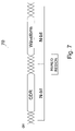
- FIG. 7 illustrates the use of a predetermined waveform bit pattern to perform waveform data sweeps at a first period of time and then CDR data tracking for synchronization at a second period of time according to an embodiment of the present invention.
- a switch is provided in waveform select logic 503 of FIG. 5 .
- the switch toggles between CDR tracking and obtaining a representation of a waveform in response to a waveform enable signal on line 560 .
- Serial data ‘din’ includes N-bits of CDR data during a first period of time followed by N-bits of waveform data during a second period of time as illustrated in FIG. 7 . There is an invalid region between CDR tracking data and waveform data. Obtaining a representation of a waveform and CDR tracking would be alternated in a continuous manner.
- FIG. 8 illustrates a multiple links embodiment of the present invention.
- Circuit 81 is coupled by multiple links to circuit 82 on a semiconductor substrate 80 in an embodiment of the present invention.
- transmit circuits 88 , 89 , and 90 are coupled to receive circuits 91 , 92 and 93 via links or medium 83 , 84 and 85 , respectfully.
- Transmit circuit 88 , link 83 and receive circuit 91 serve as a ‘master’ link that performs CDR tracking.
- Receive circuit 91 generates the synchronous clocking signal to receive circuits 92 and 93 via interconnect 87 . Accordingly, slave receive circuits 92 and 93 can obtain representations of waveforms by sweeping the clock signal obtained from receive circuit 91 across a period of a received signal.
- the master/slave embodiment offers the advantage of a relatively simple implementation compared to the other embodiments. However, variations across semiconductor substrate 80 cause differences in optimum sampling for the different links.
- FIG. 9 illustrates a method 900 according to an embodiment of the present invention.
- steps illustrated in FIG. 9 are carried out by hardware, software or a combination thereof.
- the steps illustrated in FIG. 9 are carried out by the components illustrated in FIGS. 3-8 .
- other steps that are not shown may be included in various embodiments of the present invention.
- Method 900 begins at step 901 where serial data is received. Serial data is then sampled as illustrated by step. 902 .
- data/edge samplers 100 may sample serial data.
- a sampling clock signal is then adjusted for sampling the incoming serial data in step 903 . Steps 902 and 903 are repeated in order to synchronize or phase lock to the incoming serial data.
- an edge clock signal is adjusted and used for sampling serial data at half rate. In alternate embodiments, other clock signals are used for synchronization.
- a determination is made whether to capture a representation of a waveform of the incoming serial.
- Step 905 If a representation of a waveform does not need to be captured, method 900 exits; otherwise an offset signal is adjusted in response to the serial data as illustrated by step 905 .
- Step 906 then illustrates sampling serial data to obtain a representation of a waveform in response to the phase adjusted clock signal. Steps 905 and 906 are then repeated until a representation of a waveform is obtained.
Abstract
Description
Claims (20)
Priority Applications (1)
| Application Number | Priority Date | Filing Date | Title |
|---|---|---|---|
| US11/445,702 US7765074B2 (en) | 2003-02-11 | 2006-06-02 | Circuit, apparatus and method for capturing a representation of a waveform from a clock-data recovery (CDR) unit |
Applications Claiming Priority (3)
| Application Number | Priority Date | Filing Date | Title |
|---|---|---|---|
| US44646703P | 2003-02-11 | 2003-02-11 | |
| US10/429,514 US7076377B2 (en) | 2003-02-11 | 2003-05-05 | Circuit, apparatus and method for capturing a representation of a waveform from a clock-data recovery (CDR) unit |
| US11/445,702 US7765074B2 (en) | 2003-02-11 | 2006-06-02 | Circuit, apparatus and method for capturing a representation of a waveform from a clock-data recovery (CDR) unit |
Related Parent Applications (1)
| Application Number | Title | Priority Date | Filing Date |
|---|---|---|---|
| US10/429,514 Continuation US7076377B2 (en) | 2003-02-11 | 2003-05-05 | Circuit, apparatus and method for capturing a representation of a waveform from a clock-data recovery (CDR) unit |
Publications (2)
| Publication Number | Publication Date |
|---|---|
| US20060224339A1 US20060224339A1 (en) | 2006-10-05 |
| US7765074B2 true US7765074B2 (en) | 2010-07-27 |
Family
ID=32829631
Family Applications (2)
| Application Number | Title | Priority Date | Filing Date |
|---|---|---|---|
| US10/429,514 Expired - Lifetime US7076377B2 (en) | 2003-02-11 | 2003-05-05 | Circuit, apparatus and method for capturing a representation of a waveform from a clock-data recovery (CDR) unit |
| US11/445,702 Expired - Fee Related US7765074B2 (en) | 2003-02-11 | 2006-06-02 | Circuit, apparatus and method for capturing a representation of a waveform from a clock-data recovery (CDR) unit |
Family Applications Before (1)
| Application Number | Title | Priority Date | Filing Date |
|---|---|---|---|
| US10/429,514 Expired - Lifetime US7076377B2 (en) | 2003-02-11 | 2003-05-05 | Circuit, apparatus and method for capturing a representation of a waveform from a clock-data recovery (CDR) unit |
Country Status (1)
| Country | Link |
|---|---|
| US (2) | US7076377B2 (en) |
Cited By (7)
| Publication number | Priority date | Publication date | Assignee | Title |
|---|---|---|---|---|
| US20100053454A1 (en) * | 2008-09-04 | 2010-03-04 | Fujitsu Component Limited | Receiver and signal transmission system |
| US20110289341A1 (en) * | 2008-06-30 | 2011-11-24 | Ganesh Balamurugan | Clock and data recovery (cdr) method and apparatus |
| US20150003842A1 (en) * | 2013-06-26 | 2015-01-01 | Huawei Technologies Co., Ltd. | Clock recovery circuit, optical receiver, and passive optical network device |
| CN104300968A (en) * | 2013-07-18 | 2015-01-21 | 瑞昱半导体股份有限公司 | Clock pulse and data reply device, sampler and sampling method |
| US9071234B2 (en) | 2013-03-07 | 2015-06-30 | Raytheon Company | High-resolution link-path delay estimator and method for estimating a signal-path delay |
| US9198150B2 (en) | 2013-03-07 | 2015-11-24 | Raytheon Company | Link path delay estimator that combines coarse and fine delay estimates |
| US10495727B2 (en) | 2017-02-07 | 2019-12-03 | Raytheon Company | Phase difference estimator and method for estimating a phase difference between signals |
Families Citing this family (50)
| Publication number | Priority date | Publication date | Assignee | Title |
|---|---|---|---|---|
| US6646953B1 (en) | 2000-07-06 | 2003-11-11 | Rambus Inc. | Single-clock, strobeless signaling system |
| US6643787B1 (en) | 1999-10-19 | 2003-11-04 | Rambus Inc. | Bus system optimization |
| US7349507B2 (en) * | 2003-06-09 | 2008-03-25 | Intel Corporation | Extending PPM tolerance using a tracking data recovery algorithm in a data recovery circuit |
| KR100546368B1 (en) * | 2003-08-22 | 2006-01-26 | 삼성전자주식회사 | Memory device for itself compensating clock skew occurring centering error and clock skew compensating method |
| US7280628B1 (en) * | 2003-10-14 | 2007-10-09 | Xilinx, Inc. | Data capture for a source synchronous interface |
| KR100590204B1 (en) * | 2003-11-04 | 2006-06-15 | 삼성전자주식회사 | Integrated circuit device with on-chip setup/hold measuring circuit |
| US7376211B2 (en) * | 2004-01-28 | 2008-05-20 | Texas Instruments Incorporated | High speed early/late discrimination systems and methods for clock and data recovery receivers |
| US7516029B2 (en) * | 2004-06-09 | 2009-04-07 | Rambus, Inc. | Communication channel calibration using feedback |
| US7421050B2 (en) * | 2004-10-14 | 2008-09-02 | Agere Systems Inc. | Parallel sampled multi-stage decimated digital loop filter for clock/data recovery |
| US7577224B2 (en) * | 2004-12-28 | 2009-08-18 | Silicon Laboratories Inc. | Reducing phase offsets in a phase detector |
| US7681063B2 (en) * | 2005-03-30 | 2010-03-16 | Infineon Technologies Ag | Clock data recovery circuit with circuit loop disablement |
| US7643593B1 (en) * | 2005-10-14 | 2010-01-05 | National Semiconductor Corporation | System and method for read data recovery in a serial interface |
| US7664215B2 (en) * | 2005-12-21 | 2010-02-16 | Intel Corporation | Signal alignment based on data signal |
| WO2007114944A2 (en) | 2006-04-04 | 2007-10-11 | Rambus, Inc. | Phase control block for managing multiple clock domains in systems with frequency offsets |
| US7639737B2 (en) | 2006-04-27 | 2009-12-29 | Rambus Inc. | Adaptive equalization using correlation of edge samples with data patterns |
| US8504862B2 (en) | 2007-02-20 | 2013-08-06 | Fujitsu Semiconductor Limited | Device and method for preventing lost synchronization |
| US8050371B2 (en) * | 2007-04-27 | 2011-11-01 | Freescale Semiconductor, Inc. | Method and system for compensating for the effect of phase drift in a data sampling clock |
| US7925913B1 (en) | 2007-05-04 | 2011-04-12 | Altera Corporation | CDR control architecture for robust low-latency exit from the power-saving mode of an embedded CDR in a programmable integrated circuit device |
| CN101388665B (en) * | 2007-09-14 | 2011-11-09 | 瑞昱半导体股份有限公司 | Time-interleaved clock-data recovery device and method thereof |
| DE102008011845A1 (en) * | 2007-09-21 | 2009-04-02 | Rohde & Schwarz Gmbh & Co. Kg | Method and device for clock recovery |
| JP2009194741A (en) * | 2008-02-15 | 2009-08-27 | Nec Corp | Pulse phase adjusting method and device |
| US8467436B1 (en) | 2009-04-29 | 2013-06-18 | Pmc-Sierra Us, Inc. | DSP-based diagnostics for monitoring a SerDes link |
| US8699647B2 (en) * | 2009-06-23 | 2014-04-15 | Intel Mobile Communications GmbH | Fast phase alignment for clock and data recovery |
| JP2011171808A (en) * | 2010-02-16 | 2011-09-01 | Renesas Electronics Corp | Semiconductor device and method of testing the same |
| WO2013039624A1 (en) * | 2011-09-12 | 2013-03-21 | Rambus Inc. | Offset and decision feedback equalization calibration |
| WO2013101117A1 (en) * | 2011-12-29 | 2013-07-04 | Intel Corporation | Digital clock placement engine apparatus and method with duty cycle correction and quadrature placement |
| US9363071B2 (en) | 2013-03-07 | 2016-06-07 | Qualcomm Incorporated | Circuit to recover a clock signal from multiple wire data signals that changes state every state cycle and is immune to data inter-lane skew as well as data state transition glitches |
| US9313058B2 (en) | 2013-03-07 | 2016-04-12 | Qualcomm Incorporated | Compact and fast N-factorial single data rate clock and data recovery circuits |
| US9374216B2 (en) | 2013-03-20 | 2016-06-21 | Qualcomm Incorporated | Multi-wire open-drain link with data symbol transition based clocking |
| TW201503596A (en) * | 2013-07-11 | 2015-01-16 | Realtek Semiconductor Corp | Clock and data recovery device, sampler and sampling method thereof |
| US9755818B2 (en) | 2013-10-03 | 2017-09-05 | Qualcomm Incorporated | Method to enhance MIPI D-PHY link rate with minimal PHY changes and no protocol changes |
| US9203599B2 (en) | 2014-04-10 | 2015-12-01 | Qualcomm Incorporated | Multi-lane N-factorial (N!) and other multi-wire communication systems |
| US9735948B2 (en) | 2013-10-03 | 2017-08-15 | Qualcomm Incorporated | Multi-lane N-factorial (N!) and other multi-wire communication systems |
| US9294260B2 (en) | 2013-12-27 | 2016-03-22 | Intel Corporation | Phase adjustment circuit for clock and data recovery circuit |
| TWI519119B (en) * | 2014-04-17 | 2016-01-21 | 創意電子股份有限公司 | Clock data recovery circuit and method |
| US9608798B2 (en) | 2014-06-02 | 2017-03-28 | Mediatek Inc. | Method for performing phase shift control for timing recovery in an electronic device, and associated apparatus |
| US9379921B2 (en) | 2014-08-25 | 2016-06-28 | Mediatek Inc. | Method for performing data sampling control in an electronic device, and associated apparatus |
| US9184909B1 (en) * | 2015-01-12 | 2015-11-10 | Analog Devices, Inc. | Apparatus and methods for clock and data recovery |
| US9209962B1 (en) * | 2015-05-18 | 2015-12-08 | Inphi Corporation | High-speed clock skew correction for serdes receivers |
| US9755819B2 (en) | 2015-07-01 | 2017-09-05 | Rambus Inc. | Phase calibration of clock signals |
| US9832009B2 (en) | 2015-07-28 | 2017-11-28 | Rambus Inc. | Collaborative clock and data recovery |
| US9654116B1 (en) | 2015-10-27 | 2017-05-16 | Mediatek Inc. | Clock generator using resistive components to generate sub-gate delays and/or using common-mode voltage based frequency-locked loop circuit for frequency offset reduction |
| EP3163754A1 (en) * | 2015-10-27 | 2017-05-03 | MediaTek Inc. | Method for performing phase shift control for timing recovery in an electronic device, and associated apparatus |
| US10270628B1 (en) * | 2016-05-06 | 2019-04-23 | Inphi Corporation | Method and system for calibrating equalizers |
| US10177897B2 (en) * | 2016-10-07 | 2019-01-08 | Analog Devices, Inc. | Method and system for synchronizing and interleaving separate sampler groups |
| US10447464B2 (en) * | 2017-12-05 | 2019-10-15 | Qualcomm Incorporated | Super-speed UART with pre-frame bit-rate and independent variable upstream and downstream rates |
| JP2020141203A (en) * | 2019-02-27 | 2020-09-03 | キオクシア株式会社 | Clock regenerative circuit and receiving device |
| KR20200131073A (en) * | 2019-05-13 | 2020-11-23 | 삼성전자주식회사 | Memory controller, and memory system including the same and method thereof |
| US11031939B1 (en) * | 2020-03-19 | 2021-06-08 | Mellanox Technologies, Ltd. | Phase detector command propagation between lanes in MCM USR serdes |
| US11870880B2 (en) * | 2022-01-31 | 2024-01-09 | Samsung Display Co., Ltd. | Clock data recovery (CDR) with multiple proportional path controls |
Citations (98)
| Publication number | Priority date | Publication date | Assignee | Title |
|---|---|---|---|---|
| US3869580A (en) | 1971-11-15 | 1975-03-04 | Milgo Electronic Corp | Apparatus for testing data modems which simultaneously transmit and receive frequency multiplexed signals |
| US3909563A (en) | 1973-11-06 | 1975-09-30 | Wescom | Procedure and apparatus for locating faults in digital repeatered lines |
| US4271514A (en) | 1978-09-06 | 1981-06-02 | Te Ka De, Felten & Guilleaume, Fernmeldeanlagen Gmbh | Loopback test for data transmission paths |
| US4475210A (en) | 1982-02-26 | 1984-10-02 | International Telephone And Telegraph Corporation | Data eye monitor |
| US4727540A (en) | 1984-11-30 | 1988-02-23 | Compagnie Industrielle Des Telecommications Cit-Alcatel | Apparatus for remote signalling on a digital transmission link |
| EP0333942A1 (en) | 1988-03-22 | 1989-09-27 | Hewlett-Packard Limited | Monitoring of digital transmission systems |
| JPH04147071A (en) | 1990-10-09 | 1992-05-20 | Nec Corp | Test circuit |
| US5142495A (en) | 1989-03-10 | 1992-08-25 | Intel Corporation | Variable load for margin mode |
| JPH04246921A (en) | 1991-01-31 | 1992-09-02 | Nec Corp | Pattern testing system |
| US5197062A (en) | 1991-09-04 | 1993-03-23 | Picklesimer David D | Method and system for simultaneous analysis of multiplexed channels |
| US5228042A (en) | 1991-02-07 | 1993-07-13 | Northern Telecom Limited | Method and circuit for testing transmission paths |
| US5258986A (en) | 1990-09-19 | 1993-11-02 | Vlsi Technology, Inc. | Tightly coupled, low overhead RAM built-in self-test logic with particular applications for embedded memories |
| US5265089A (en) | 1990-01-30 | 1993-11-23 | Nec Corporation | Loopback test circuit |
| US5369755A (en) | 1992-09-08 | 1994-11-29 | Alliedsignal Inc. | Computer communication bus system using multiple content induced transaction overlap (CITO) communication channels |
| US5383177A (en) | 1993-09-20 | 1995-01-17 | Fujitsu Limited | Packet switching testing method and apparatus |
| US5392298A (en) | 1991-07-11 | 1995-02-21 | Nec Corporation | Testing apparatus for exactly discriminating defective product from acceptable product and testing method used therein |
| US5412665A (en) | 1992-01-10 | 1995-05-02 | International Business Machines Corporation | Parallel operation linear feedback shift register |
| US5430736A (en) | 1991-04-16 | 1995-07-04 | Matsushita Electric Industrial, Co., Ltd. | Method and apparatus for generating test pattern for sequential logic circuit of integrated circuit |
| US5444715A (en) | 1992-07-17 | 1995-08-22 | International Business Machines Corporation | AC interconnect test of integrated circuit chips |
| US5473619A (en) | 1991-04-08 | 1995-12-05 | Sharp Kabushiki Kaisha | Method and apparatus for testing a driving circuit |
| US5483676A (en) | 1988-08-04 | 1996-01-09 | Norand Corporation | Mobile radio data communication system and method |
| US5485473A (en) | 1992-08-25 | 1996-01-16 | Diebold; Ulich | Method and system for testing an integrated circuit featuring scan design |
| US5490150A (en) | 1992-09-18 | 1996-02-06 | At&T Corp. | Method and apparatus for data parity in a transmission system |
| US5519719A (en) | 1991-12-19 | 1996-05-21 | Adc Telecommunications, Inc. | Universal pattern generator |
| US5675588A (en) | 1993-09-20 | 1997-10-07 | Fujitsu Limited | Testing apparatus for transmission system |
| US5732089A (en) | 1995-09-27 | 1998-03-24 | Ando Electric Co., Ltd. | Bit error measurement circuit |
| US5742798A (en) | 1996-08-09 | 1998-04-21 | International Business Machines Corporation | Compensation of chip to chip clock skew |
| US5761216A (en) | 1995-02-24 | 1998-06-02 | Advantest Corp. | Bit error measurement system |
| US5761212A (en) | 1993-07-01 | 1998-06-02 | Cirrus Logic, Inc. | Channel quality |
| US5790523A (en) | 1993-09-17 | 1998-08-04 | Scientific-Atlanta, Inc. | Testing facility for a broadband communications system |
| US5802073A (en) | 1994-09-23 | 1998-09-01 | Vlsi Technology, Inc. | Built-in self test functional system block for UTOPIA interface |
| US5812619A (en) * | 1996-02-28 | 1998-09-22 | Advanced Micro Devices, Inc. | Digital phase lock loop and system for digital clock recovery |
| US5815017A (en) | 1997-03-03 | 1998-09-29 | Motorola, Inc. | Forced oscillator circuit and method |
| US5831996A (en) | 1996-10-10 | 1998-11-03 | Lucent Technologies Inc. | Digital circuit test generator |
| US5841271A (en) | 1993-11-17 | 1998-11-24 | Nec Corporation | Test mode power circuit for integrated-circuit chip |
| US5875177A (en) | 1991-09-12 | 1999-02-23 | Fujitsu Limited | Path test system for ATM switch |
| US5917856A (en) | 1994-10-31 | 1999-06-29 | Nokia Telecommunications Oy | Method for establishing a PAM signal connection using a training sequence |
| US5938784A (en) | 1996-10-21 | 1999-08-17 | Samsung Electronics, Co., Ltd. | Linear feedback shift register, multiple input signature register, and built-in self test circuit using such registers |
| US5999022A (en) | 1995-04-17 | 1999-12-07 | Matsushita Electric Industrial Co., Ltd. | Signal transmission driver circuit, receiver circuit, and method thereof for transmitting and receiving information based on multiple periods and/or a delay function |
| US6003118A (en) | 1997-12-16 | 1999-12-14 | Acer Laboratories Inc. | Method and apparatus for synchronizing clock distribution of a data processing system |
| US6005632A (en) | 1996-12-20 | 1999-12-21 | Intel Corporation | Method and apparatus for supporting variable sampling rates when decoding vertical blanking interval data |
| JP2000035831A (en) | 1998-07-21 | 2000-02-02 | Nec Corp | Low skew clock tree circuit using variable threshold voltage transistor |
| US6055297A (en) | 1996-08-02 | 2000-04-25 | Northern Telecom Limited | Reducing crosstalk between communications systems |
| US6061817A (en) | 1996-06-10 | 2000-05-09 | Cypress Semiconductor Corp. | Method and apparatus for generating test pattern for sequence detection |
| US6073263A (en) | 1997-10-29 | 2000-06-06 | Credence Systems Corporation | Parallel processing pattern generation system for an integrated circuit tester |
| US6154659A (en) | 1997-12-24 | 2000-11-28 | Nortel Networks Limited | Fast forward link power control in a code division multiple access system |
| US6160860A (en) * | 1998-01-28 | 2000-12-12 | Lucent Technologies Inc. | Phase-locked loop (PLL) circuit containing a frequency detector for improved frequency acquisition |
| US6160790A (en) | 1996-12-31 | 2000-12-12 | Paradyne Corporation | Crosstalk canceller system and method |
| US6201829B1 (en) | 1998-04-03 | 2001-03-13 | Adaptec, Inc. | Serial/parallel GHZ transceiver with pseudo-random built in self test pattern generator |
| US6222380B1 (en) | 1998-06-15 | 2001-04-24 | International Business Machines Corporation | High speed parallel/serial link for data communication |
| US6230022B1 (en) | 1997-12-27 | 2001-05-08 | Sony Corporation | Transmitting method and apparatus, and sending power controlling method |
| US20010016929A1 (en) | 1999-12-22 | 2001-08-23 | International Business Machines Corporation | Built-in self test system and method for high speed clock and data recovery circuit |
| US6289045B1 (en) | 1998-07-07 | 2001-09-11 | Fujitsu Limited | Training method in a time domain equalizer and a digital data transmission apparatus including an improved training apparatus |
| US20010021987A1 (en) | 1999-07-14 | 2001-09-13 | Madabusi Govindarajan | Method and apparatus for performance monitoring of data transparent communication links |
| US6292116B1 (en) | 1999-05-17 | 2001-09-18 | Altera Corporation | Techniques and circuitry for accurately sampling high frequency data signals input to an integrated circuit |
| EP1134668A2 (en) | 2000-03-15 | 2001-09-19 | Lucent Technologies Inc. | Data communication link between two ASICs |
| US20010034866A1 (en) | 2000-01-14 | 2001-10-25 | Barry John Lee | Algorithmic test pattern generator, with built-in-self-test (BIST) capabilities, for functional testing of a circuit |
| US6326852B1 (en) | 1998-09-21 | 2001-12-04 | Broadcom Corporation | Low offset and low glitch energy charge pump for PLL-based timing recovery systems |
| US6331787B1 (en) | 1997-05-07 | 2001-12-18 | California Micro Devices Corporation | Termination circuits and methods therefor |
| US6339387B1 (en) | 1997-05-21 | 2002-01-15 | Fujitsu Limited | Serial/parallel converter |
| US6378079B1 (en) | 1998-02-27 | 2002-04-23 | Micron Technology, Inc. | Computer system having memory device with adjustable data clocking |
| US6385236B1 (en) | 1998-10-05 | 2002-05-07 | Lsi Logic Corporation | Method and Circuit for testing devices with serial data links |
| US20020059546A1 (en) | 2000-09-13 | 2002-05-16 | Hirofumi Yonetoku | Method of generating a pattern for testing a logic circuit and apparatus for doing the same |
| US20020059545A1 (en) | 2000-11-10 | 2002-05-16 | Wataru Nakashima | Apparatus for testing functions of communication apparatus |
| US20020073373A1 (en) | 2000-12-13 | 2002-06-13 | Michinobu Nakao | Test method of semiconductor intergrated circuit and test pattern generator |
| US6407572B1 (en) | 1999-09-03 | 2002-06-18 | Fujitsu Limited | System and method for testing and evaluating a device |
| US6421801B1 (en) | 1999-06-08 | 2002-07-16 | Intel Corporation | Testing IO timing in a delay locked system using separate transmit and receive loops |
| US20020108079A1 (en) | 2001-02-02 | 2002-08-08 | Koji Takahashi | Test pattern conversion apparatus and conversion method |
| US6438159B1 (en) | 1999-02-16 | 2002-08-20 | Maxtor Corporation | Method and apparatus for margining error rate of multi-drop data buses |
| US20020138800A1 (en) | 2001-03-13 | 2002-09-26 | Samsung Electronics Co., Ltd. | Built-in self test circuit employing a linear feedback shift register |
| US6463109B1 (en) * | 1998-08-25 | 2002-10-08 | Vitesse Semiconductor Corporation | Multiple channel adaptive data recovery system |
| US20020146084A1 (en) * | 2001-02-02 | 2002-10-10 | International Business Machines Corporation | Apparatus and method for oversampling with evenly spaced samples |
| US6473871B1 (en) | 1999-08-31 | 2002-10-29 | Sun Microsystems, Inc. | Method and apparatus for HASS testing of busses under programmable control |
| US6477674B1 (en) | 1999-12-29 | 2002-11-05 | Intel Corporation | Method and apparatus for conducting input/output loop back tests using a local pattern generator and delay elements |
| US20020178412A1 (en) | 1998-07-01 | 2002-11-28 | Noriyuki Matsui | Memory testing method and apparatus, and computer-readable recording medium |
| US20030065995A1 (en) | 2001-08-15 | 2003-04-03 | Psytechnics Limited | Communication channel accuracy measurement |
| US20030070118A1 (en) | 2001-10-09 | 2003-04-10 | Hitachi, Ltd. | Semiconductor integrated circuit with built-in test function |
| US20030086517A1 (en) | 2001-10-26 | 2003-05-08 | International Business Machines Corporation | Method and circuit for recovering a data signal from a stream of binary data |
| US20030088818A1 (en) | 1998-09-03 | 2003-05-08 | Manning Troy A. | Method and apparatus for generating expect data from a captured bit pattern, and memory device using same |
| US6574758B1 (en) | 2000-03-10 | 2003-06-03 | Cisco Technology, Inc. | Testing a bus coupled between two electronic devices |
| US20030131297A1 (en) | 2000-01-10 | 2003-07-10 | Fischel Scott Eduard | Method and apparatus for testing wireless communication channels |
| US6606041B1 (en) | 2000-05-10 | 2003-08-12 | Micron Technology, Inc. | Predictive timing calibration for memory devices |
| US6611928B1 (en) | 2000-01-07 | 2003-08-26 | Fujitsu Limited | Homo-code continuity proof testing device |
| US6615148B2 (en) * | 2000-05-17 | 2003-09-02 | Tektronix, Inc. | Streaming distributed test and measurement instrument |
| US6625764B1 (en) | 2000-11-28 | 2003-09-23 | Nortel Networks Limited | Testing using test packets containing random data |
| US6628621B1 (en) | 1999-11-02 | 2003-09-30 | Adtran Inc. | Multichannel-capable bit error rate test system |
| US6631486B1 (en) | 1998-09-29 | 2003-10-07 | Matsushita Electric Industrial Co., Ltd. | Semiconductor integrated circuit and method for testing the same |
| US6650698B1 (en) | 1999-09-29 | 2003-11-18 | Conexant Systems, Inc. | Non-linear equalization for the upstream data connection of 56K PCM modems |
| US6671847B1 (en) | 2000-11-08 | 2003-12-30 | Intel Corporation | I/O device testing method and apparatus |
| US6674998B2 (en) | 2000-10-02 | 2004-01-06 | Intersil Americas Inc. | System and method for detecting and correcting phase error between differential signals |
| US6684351B1 (en) | 2000-12-22 | 2004-01-27 | Applied Micro Circuits Corporation | System and method for diagnosing errors in multidimensional digital frame structure communications |
| US6684350B1 (en) | 2000-12-22 | 2004-01-27 | Cisco Technology, Inc. | Repetitive pattern testing circuit for AC-coupled systems |
| US6693881B1 (en) | 1998-05-29 | 2004-02-17 | Alcatel | Method for bit error rate measurements in a cell-based telecommunication system |
| US6694466B1 (en) | 1999-10-27 | 2004-02-17 | Agere Systems Inc. | Method and system for improving the test quality for scan-based BIST using a general test application scheme |
| US20040114698A1 (en) | 2001-02-24 | 2004-06-17 | Barrett Wayne Melvin | Data capture technique for high speed signaling |
| US6977959B2 (en) * | 2003-01-17 | 2005-12-20 | Xilinx, Inc. | Clock and data recovery phase-locked loop |
| JP4147071B2 (en) | 2002-08-29 | 2008-09-10 | 株式会社リコー | Image forming system, image forming apparatus, information processing apparatus, and program in information processing apparatus |
| JP4246921B2 (en) | 1998-11-12 | 2009-04-02 | 富士通株式会社 | Method and apparatus for preventing toggle switching between two zones of a wireless communication network |
Family Cites Families (3)
| Publication number | Priority date | Publication date | Assignee | Title |
|---|---|---|---|---|
| JPH04156505A (en) * | 1990-10-20 | 1992-05-29 | Fuji Photo Optical Co Ltd | Lens adhesion-fixing method to lens supporter for constituting optical system |
| US6223380B1 (en) * | 1999-04-27 | 2001-05-01 | Sunex L.L.C. | Surface contacting with spray bottle dispensers |
| US6553795B1 (en) * | 1999-08-30 | 2003-04-29 | Knox Company | Locking cover plate arrangement |
-
2003
- 2003-05-05 US US10/429,514 patent/US7076377B2/en not_active Expired - Lifetime
-
2006
- 2006-06-02 US US11/445,702 patent/US7765074B2/en not_active Expired - Fee Related
Patent Citations (98)
| Publication number | Priority date | Publication date | Assignee | Title |
|---|---|---|---|---|
| US3869580A (en) | 1971-11-15 | 1975-03-04 | Milgo Electronic Corp | Apparatus for testing data modems which simultaneously transmit and receive frequency multiplexed signals |
| US3909563A (en) | 1973-11-06 | 1975-09-30 | Wescom | Procedure and apparatus for locating faults in digital repeatered lines |
| US4271514A (en) | 1978-09-06 | 1981-06-02 | Te Ka De, Felten & Guilleaume, Fernmeldeanlagen Gmbh | Loopback test for data transmission paths |
| US4475210A (en) | 1982-02-26 | 1984-10-02 | International Telephone And Telegraph Corporation | Data eye monitor |
| US4727540A (en) | 1984-11-30 | 1988-02-23 | Compagnie Industrielle Des Telecommications Cit-Alcatel | Apparatus for remote signalling on a digital transmission link |
| EP0333942A1 (en) | 1988-03-22 | 1989-09-27 | Hewlett-Packard Limited | Monitoring of digital transmission systems |
| US5483676A (en) | 1988-08-04 | 1996-01-09 | Norand Corporation | Mobile radio data communication system and method |
| US5142495A (en) | 1989-03-10 | 1992-08-25 | Intel Corporation | Variable load for margin mode |
| US5265089A (en) | 1990-01-30 | 1993-11-23 | Nec Corporation | Loopback test circuit |
| US5258986A (en) | 1990-09-19 | 1993-11-02 | Vlsi Technology, Inc. | Tightly coupled, low overhead RAM built-in self-test logic with particular applications for embedded memories |
| JPH04147071A (en) | 1990-10-09 | 1992-05-20 | Nec Corp | Test circuit |
| JPH04246921A (en) | 1991-01-31 | 1992-09-02 | Nec Corp | Pattern testing system |
| US5228042A (en) | 1991-02-07 | 1993-07-13 | Northern Telecom Limited | Method and circuit for testing transmission paths |
| US5473619A (en) | 1991-04-08 | 1995-12-05 | Sharp Kabushiki Kaisha | Method and apparatus for testing a driving circuit |
| US5430736A (en) | 1991-04-16 | 1995-07-04 | Matsushita Electric Industrial, Co., Ltd. | Method and apparatus for generating test pattern for sequential logic circuit of integrated circuit |
| US5392298A (en) | 1991-07-11 | 1995-02-21 | Nec Corporation | Testing apparatus for exactly discriminating defective product from acceptable product and testing method used therein |
| US5197062A (en) | 1991-09-04 | 1993-03-23 | Picklesimer David D | Method and system for simultaneous analysis of multiplexed channels |
| US5875177A (en) | 1991-09-12 | 1999-02-23 | Fujitsu Limited | Path test system for ATM switch |
| US5519719A (en) | 1991-12-19 | 1996-05-21 | Adc Telecommunications, Inc. | Universal pattern generator |
| US5412665A (en) | 1992-01-10 | 1995-05-02 | International Business Machines Corporation | Parallel operation linear feedback shift register |
| US5444715A (en) | 1992-07-17 | 1995-08-22 | International Business Machines Corporation | AC interconnect test of integrated circuit chips |
| US5485473A (en) | 1992-08-25 | 1996-01-16 | Diebold; Ulich | Method and system for testing an integrated circuit featuring scan design |
| US5369755A (en) | 1992-09-08 | 1994-11-29 | Alliedsignal Inc. | Computer communication bus system using multiple content induced transaction overlap (CITO) communication channels |
| US5490150A (en) | 1992-09-18 | 1996-02-06 | At&T Corp. | Method and apparatus for data parity in a transmission system |
| US5761212A (en) | 1993-07-01 | 1998-06-02 | Cirrus Logic, Inc. | Channel quality |
| US5790523A (en) | 1993-09-17 | 1998-08-04 | Scientific-Atlanta, Inc. | Testing facility for a broadband communications system |
| US5675588A (en) | 1993-09-20 | 1997-10-07 | Fujitsu Limited | Testing apparatus for transmission system |
| US5383177A (en) | 1993-09-20 | 1995-01-17 | Fujitsu Limited | Packet switching testing method and apparatus |
| US5841271A (en) | 1993-11-17 | 1998-11-24 | Nec Corporation | Test mode power circuit for integrated-circuit chip |
| US5802073A (en) | 1994-09-23 | 1998-09-01 | Vlsi Technology, Inc. | Built-in self test functional system block for UTOPIA interface |
| US5917856A (en) | 1994-10-31 | 1999-06-29 | Nokia Telecommunications Oy | Method for establishing a PAM signal connection using a training sequence |
| US5761216A (en) | 1995-02-24 | 1998-06-02 | Advantest Corp. | Bit error measurement system |
| US5999022A (en) | 1995-04-17 | 1999-12-07 | Matsushita Electric Industrial Co., Ltd. | Signal transmission driver circuit, receiver circuit, and method thereof for transmitting and receiving information based on multiple periods and/or a delay function |
| US5732089A (en) | 1995-09-27 | 1998-03-24 | Ando Electric Co., Ltd. | Bit error measurement circuit |
| US5812619A (en) * | 1996-02-28 | 1998-09-22 | Advanced Micro Devices, Inc. | Digital phase lock loop and system for digital clock recovery |
| US6061817A (en) | 1996-06-10 | 2000-05-09 | Cypress Semiconductor Corp. | Method and apparatus for generating test pattern for sequence detection |
| US6055297A (en) | 1996-08-02 | 2000-04-25 | Northern Telecom Limited | Reducing crosstalk between communications systems |
| US5742798A (en) | 1996-08-09 | 1998-04-21 | International Business Machines Corporation | Compensation of chip to chip clock skew |
| US5831996A (en) | 1996-10-10 | 1998-11-03 | Lucent Technologies Inc. | Digital circuit test generator |
| US5938784A (en) | 1996-10-21 | 1999-08-17 | Samsung Electronics, Co., Ltd. | Linear feedback shift register, multiple input signature register, and built-in self test circuit using such registers |
| US6005632A (en) | 1996-12-20 | 1999-12-21 | Intel Corporation | Method and apparatus for supporting variable sampling rates when decoding vertical blanking interval data |
| US6160790A (en) | 1996-12-31 | 2000-12-12 | Paradyne Corporation | Crosstalk canceller system and method |
| US5815017A (en) | 1997-03-03 | 1998-09-29 | Motorola, Inc. | Forced oscillator circuit and method |
| US6331787B1 (en) | 1997-05-07 | 2001-12-18 | California Micro Devices Corporation | Termination circuits and methods therefor |
| US6339387B1 (en) | 1997-05-21 | 2002-01-15 | Fujitsu Limited | Serial/parallel converter |
| US6073263A (en) | 1997-10-29 | 2000-06-06 | Credence Systems Corporation | Parallel processing pattern generation system for an integrated circuit tester |
| US6003118A (en) | 1997-12-16 | 1999-12-14 | Acer Laboratories Inc. | Method and apparatus for synchronizing clock distribution of a data processing system |
| US6154659A (en) | 1997-12-24 | 2000-11-28 | Nortel Networks Limited | Fast forward link power control in a code division multiple access system |
| US6230022B1 (en) | 1997-12-27 | 2001-05-08 | Sony Corporation | Transmitting method and apparatus, and sending power controlling method |
| US6160860A (en) * | 1998-01-28 | 2000-12-12 | Lucent Technologies Inc. | Phase-locked loop (PLL) circuit containing a frequency detector for improved frequency acquisition |
| US6378079B1 (en) | 1998-02-27 | 2002-04-23 | Micron Technology, Inc. | Computer system having memory device with adjustable data clocking |
| US6201829B1 (en) | 1998-04-03 | 2001-03-13 | Adaptec, Inc. | Serial/parallel GHZ transceiver with pseudo-random built in self test pattern generator |
| US6693881B1 (en) | 1998-05-29 | 2004-02-17 | Alcatel | Method for bit error rate measurements in a cell-based telecommunication system |
| US6222380B1 (en) | 1998-06-15 | 2001-04-24 | International Business Machines Corporation | High speed parallel/serial link for data communication |
| US20020178412A1 (en) | 1998-07-01 | 2002-11-28 | Noriyuki Matsui | Memory testing method and apparatus, and computer-readable recording medium |
| US6289045B1 (en) | 1998-07-07 | 2001-09-11 | Fujitsu Limited | Training method in a time domain equalizer and a digital data transmission apparatus including an improved training apparatus |
| JP2000035831A (en) | 1998-07-21 | 2000-02-02 | Nec Corp | Low skew clock tree circuit using variable threshold voltage transistor |
| US6463109B1 (en) * | 1998-08-25 | 2002-10-08 | Vitesse Semiconductor Corporation | Multiple channel adaptive data recovery system |
| US20030088818A1 (en) | 1998-09-03 | 2003-05-08 | Manning Troy A. | Method and apparatus for generating expect data from a captured bit pattern, and memory device using same |
| US6326852B1 (en) | 1998-09-21 | 2001-12-04 | Broadcom Corporation | Low offset and low glitch energy charge pump for PLL-based timing recovery systems |
| US6631486B1 (en) | 1998-09-29 | 2003-10-07 | Matsushita Electric Industrial Co., Ltd. | Semiconductor integrated circuit and method for testing the same |
| US6385236B1 (en) | 1998-10-05 | 2002-05-07 | Lsi Logic Corporation | Method and Circuit for testing devices with serial data links |
| JP4246921B2 (en) | 1998-11-12 | 2009-04-02 | 富士通株式会社 | Method and apparatus for preventing toggle switching between two zones of a wireless communication network |
| US6438159B1 (en) | 1999-02-16 | 2002-08-20 | Maxtor Corporation | Method and apparatus for margining error rate of multi-drop data buses |
| US6292116B1 (en) | 1999-05-17 | 2001-09-18 | Altera Corporation | Techniques and circuitry for accurately sampling high frequency data signals input to an integrated circuit |
| US6421801B1 (en) | 1999-06-08 | 2002-07-16 | Intel Corporation | Testing IO timing in a delay locked system using separate transmit and receive loops |
| US20010021987A1 (en) | 1999-07-14 | 2001-09-13 | Madabusi Govindarajan | Method and apparatus for performance monitoring of data transparent communication links |
| US6473871B1 (en) | 1999-08-31 | 2002-10-29 | Sun Microsystems, Inc. | Method and apparatus for HASS testing of busses under programmable control |
| US6407572B1 (en) | 1999-09-03 | 2002-06-18 | Fujitsu Limited | System and method for testing and evaluating a device |
| US6650698B1 (en) | 1999-09-29 | 2003-11-18 | Conexant Systems, Inc. | Non-linear equalization for the upstream data connection of 56K PCM modems |
| US6694466B1 (en) | 1999-10-27 | 2004-02-17 | Agere Systems Inc. | Method and system for improving the test quality for scan-based BIST using a general test application scheme |
| US6628621B1 (en) | 1999-11-02 | 2003-09-30 | Adtran Inc. | Multichannel-capable bit error rate test system |
| US20010016929A1 (en) | 1999-12-22 | 2001-08-23 | International Business Machines Corporation | Built-in self test system and method for high speed clock and data recovery circuit |
| US6477674B1 (en) | 1999-12-29 | 2002-11-05 | Intel Corporation | Method and apparatus for conducting input/output loop back tests using a local pattern generator and delay elements |
| US6611928B1 (en) | 2000-01-07 | 2003-08-26 | Fujitsu Limited | Homo-code continuity proof testing device |
| US20030131297A1 (en) | 2000-01-10 | 2003-07-10 | Fischel Scott Eduard | Method and apparatus for testing wireless communication channels |
| US20010034866A1 (en) | 2000-01-14 | 2001-10-25 | Barry John Lee | Algorithmic test pattern generator, with built-in-self-test (BIST) capabilities, for functional testing of a circuit |
| US6574758B1 (en) | 2000-03-10 | 2003-06-03 | Cisco Technology, Inc. | Testing a bus coupled between two electronic devices |
| EP1134668A2 (en) | 2000-03-15 | 2001-09-19 | Lucent Technologies Inc. | Data communication link between two ASICs |
| US6606041B1 (en) | 2000-05-10 | 2003-08-12 | Micron Technology, Inc. | Predictive timing calibration for memory devices |
| US6615148B2 (en) * | 2000-05-17 | 2003-09-02 | Tektronix, Inc. | Streaming distributed test and measurement instrument |
| US20020059546A1 (en) | 2000-09-13 | 2002-05-16 | Hirofumi Yonetoku | Method of generating a pattern for testing a logic circuit and apparatus for doing the same |
| US6674998B2 (en) | 2000-10-02 | 2004-01-06 | Intersil Americas Inc. | System and method for detecting and correcting phase error between differential signals |
| US6671847B1 (en) | 2000-11-08 | 2003-12-30 | Intel Corporation | I/O device testing method and apparatus |
| US20020059545A1 (en) | 2000-11-10 | 2002-05-16 | Wataru Nakashima | Apparatus for testing functions of communication apparatus |
| US6625764B1 (en) | 2000-11-28 | 2003-09-23 | Nortel Networks Limited | Testing using test packets containing random data |
| US20020073373A1 (en) | 2000-12-13 | 2002-06-13 | Michinobu Nakao | Test method of semiconductor intergrated circuit and test pattern generator |
| US6684351B1 (en) | 2000-12-22 | 2004-01-27 | Applied Micro Circuits Corporation | System and method for diagnosing errors in multidimensional digital frame structure communications |
| US6684350B1 (en) | 2000-12-22 | 2004-01-27 | Cisco Technology, Inc. | Repetitive pattern testing circuit for AC-coupled systems |
| US20020108079A1 (en) | 2001-02-02 | 2002-08-08 | Koji Takahashi | Test pattern conversion apparatus and conversion method |
| US20020146084A1 (en) * | 2001-02-02 | 2002-10-10 | International Business Machines Corporation | Apparatus and method for oversampling with evenly spaced samples |
| US20040114698A1 (en) | 2001-02-24 | 2004-06-17 | Barrett Wayne Melvin | Data capture technique for high speed signaling |
| US20020138800A1 (en) | 2001-03-13 | 2002-09-26 | Samsung Electronics Co., Ltd. | Built-in self test circuit employing a linear feedback shift register |
| US20030065995A1 (en) | 2001-08-15 | 2003-04-03 | Psytechnics Limited | Communication channel accuracy measurement |
| US20030070118A1 (en) | 2001-10-09 | 2003-04-10 | Hitachi, Ltd. | Semiconductor integrated circuit with built-in test function |
| US20030086517A1 (en) | 2001-10-26 | 2003-05-08 | International Business Machines Corporation | Method and circuit for recovering a data signal from a stream of binary data |
| JP4147071B2 (en) | 2002-08-29 | 2008-09-10 | 株式会社リコー | Image forming system, image forming apparatus, information processing apparatus, and program in information processing apparatus |
| US6977959B2 (en) * | 2003-01-17 | 2005-12-20 | Xilinx, Inc. | Clock and data recovery phase-locked loop |
Non-Patent Citations (11)
| Title |
|---|
| Cova et al., Characterization of Individual Weights in Transversal Filters and Application to CCD's, IEEE Journal of Solid-State Circuits, vol. SC-17, No. 6, Dec. 1982, pp. 1054-1061. |
| Cypress Semiconductor Corporation, "HOTLink(TM) Built-In Self-Test (BIST)." Mar. 11, 1999. 13 pages. |
| Cypress Semiconductor Corporation, "HOTLink™ Built-In Self-Test (BIST)." Mar. 11, 1999. 13 pages. |
| Dally et al., "Multi-gigabit Signaling with CMOS," DARPA funded. |
| Farber et al, "Wide-Band Network Characterization by Fourier Transformation of Time-Domain Measurements," IEEE Journal of Solid-State Circuits, vol. SC-4, No. 4, Aug. 1969, pp. 231-235. |
| Ikawa, Y. et al, "Modeling of High-Speed, Large-Signal Transistor Switching Transcients from s-Parameter Measurements," IEEE Journal of Solid-State Circuits, vol. SC-17, No. 2, Apr. 1982, pp. 299-305. |
| Klein, B., "Use LFSRs to Build Fast FPGA-Based Counters," Electronic Design, pp. 87-100, Mar. 21, 1994. |
| Maxfield, C., "The Ouroboros of the Digital Consciousness: Linear-FeedbackShift Registers," EDN, pp. 135-142, Jan. 4, 1996. |
| Pfaff, A., "Test high-speed drivers with bursts and pseudorandom bit patterns," EDN, pp. 133-136, May 12, 1994 (3 pages). |
| Sato, T., et al., "Accurate in Situ Measurement of Peak Noise and Delay Change Induced by Interconnect Coupling," IEEE Journal of Solid-State Circuits, vol. 36, No. 10, Oct. 2001. pp. 1587-1591. |
| Soumyanath, K. et al, "Accurate On-Chip Interconnect Evaluation: A Time-Domain Technique." IEEE Journal of Solid-State Circuits, vol. 34, No. 5, May 1999, pp. 623-631. |
Cited By (10)
| Publication number | Priority date | Publication date | Assignee | Title |
|---|---|---|---|---|
| US20110289341A1 (en) * | 2008-06-30 | 2011-11-24 | Ganesh Balamurugan | Clock and data recovery (cdr) method and apparatus |
| US8375242B2 (en) * | 2008-06-30 | 2013-02-12 | Intel Corporation | Clock and data recovery (CDR) method and apparatus |
| US20100053454A1 (en) * | 2008-09-04 | 2010-03-04 | Fujitsu Component Limited | Receiver and signal transmission system |
| US8471835B2 (en) * | 2008-09-04 | 2013-06-25 | Fujitsu Component Limited | Receiver and signal transmission system |
| US9071234B2 (en) | 2013-03-07 | 2015-06-30 | Raytheon Company | High-resolution link-path delay estimator and method for estimating a signal-path delay |
| US9198150B2 (en) | 2013-03-07 | 2015-11-24 | Raytheon Company | Link path delay estimator that combines coarse and fine delay estimates |
| US20150003842A1 (en) * | 2013-06-26 | 2015-01-01 | Huawei Technologies Co., Ltd. | Clock recovery circuit, optical receiver, and passive optical network device |
| US9209906B2 (en) * | 2013-06-26 | 2015-12-08 | Huawei Technologies Co., Ltd. | Clock recovery circuit, optical receiver, and passive optical network device |
| CN104300968A (en) * | 2013-07-18 | 2015-01-21 | 瑞昱半导体股份有限公司 | Clock pulse and data reply device, sampler and sampling method |
| US10495727B2 (en) | 2017-02-07 | 2019-12-03 | Raytheon Company | Phase difference estimator and method for estimating a phase difference between signals |
Also Published As
| Publication number | Publication date |
|---|---|
| US20040158420A1 (en) | 2004-08-12 |
| US20060224339A1 (en) | 2006-10-05 |
| US7076377B2 (en) | 2006-07-11 |
Similar Documents
| Publication | Publication Date | Title |
|---|---|---|
| US7765074B2 (en) | Circuit, apparatus and method for capturing a representation of a waveform from a clock-data recovery (CDR) unit | |
| US11063741B2 (en) | Phase control block for managing multiple clock domains in systems with frequency offsets | |
| US6473439B1 (en) | Method and apparatus for fail-safe resynchronization with minimum latency | |
| US7142623B2 (en) | On-chip system and method for measuring jitter tolerance of a clock and data recovery circuit | |
| US7602869B2 (en) | Methods and apparatus for clock synchronization and data recovery in a receiver | |
| US8842794B2 (en) | Semiconductor device, a parallel interface system and methods thereof | |
| US20230409072A1 (en) | Drift detection in timing signal forwarded from memory controller to memory device | |
| KR101221303B1 (en) | Bit-deskewing io method and system | |
| US20060274874A1 (en) | Clock and data timing compensation for receiver | |
| KR100543646B1 (en) | Method and system of automatic delay detection and receiver adjustment for synchronous bus interface | |
| US7519844B2 (en) | PVT drift compensation | |
| CN113497701A (en) | Phase detector command propagation between channels in MCM USR SERDES | |
| US20030132783A1 (en) | Clock switching circuitry for jitter reduction | |
| US7376528B2 (en) | Devices and methods for testing clock and data recovery devices |
Legal Events
| Date | Code | Title | Description |
|---|---|---|---|
| STCF | Information on status: patent grant |
Free format text: PATENTED CASE |
|
| FPAY | Fee payment |
Year of fee payment: 4 |
|
| MAFP | Maintenance fee payment |
Free format text: PAYMENT OF MAINTENANCE FEE, 8TH YEAR, LARGE ENTITY (ORIGINAL EVENT CODE: M1552) Year of fee payment: 8 |
|
| FEPP | Fee payment procedure |
Free format text: MAINTENANCE FEE REMINDER MAILED (ORIGINAL EVENT CODE: REM.); ENTITY STATUS OF PATENT OWNER: LARGE ENTITY |
|
| LAPS | Lapse for failure to pay maintenance fees |
Free format text: PATENT EXPIRED FOR FAILURE TO PAY MAINTENANCE FEES (ORIGINAL EVENT CODE: EXP.); ENTITY STATUS OF PATENT OWNER: LARGE ENTITY |
|
| STCH | Information on status: patent discontinuation |
Free format text: PATENT EXPIRED DUE TO NONPAYMENT OF MAINTENANCE FEES UNDER 37 CFR 1.362 |
|
| FP | Lapsed due to failure to pay maintenance fee |
Effective date: 20220727 |