US7882379B2 - Power consumption reduction in a multiprocessor system - Google Patents
Power consumption reduction in a multiprocessor system Download PDFInfo
- Publication number
- US7882379B2 US7882379B2 US11/525,306 US52530606A US7882379B2 US 7882379 B2 US7882379 B2 US 7882379B2 US 52530606 A US52530606 A US 52530606A US 7882379 B2 US7882379 B2 US 7882379B2
- Authority
- US
- United States
- Prior art keywords
- frequency
- processor
- data
- waiting
- loop count
- Prior art date
- Legal status (The legal status is an assumption and is not a legal conclusion. Google has not performed a legal analysis and makes no representation as to the accuracy of the status listed.)
- Active, expires
Links
Images


Classifications
-
- G—PHYSICS
- G06—COMPUTING; CALCULATING OR COUNTING
- G06F—ELECTRIC DIGITAL DATA PROCESSING
- G06F1/00—Details not covered by groups G06F3/00 - G06F13/00 and G06F21/00
- G06F1/26—Power supply means, e.g. regulation thereof
- G06F1/32—Means for saving power
- G06F1/3203—Power management, i.e. event-based initiation of a power-saving mode
- G06F1/3234—Power saving characterised by the action undertaken
- G06F1/324—Power saving characterised by the action undertaken by lowering clock frequency
-
- G—PHYSICS
- G06—COMPUTING; CALCULATING OR COUNTING
- G06F—ELECTRIC DIGITAL DATA PROCESSING
- G06F9/00—Arrangements for program control, e.g. control units
- G06F9/06—Arrangements for program control, e.g. control units using stored programs, i.e. using an internal store of processing equipment to receive or retain programs
- G06F9/46—Multiprogramming arrangements
- G06F9/52—Program synchronisation; Mutual exclusion, e.g. by means of semaphores
- G06F9/526—Mutual exclusion algorithms
-
- Y—GENERAL TAGGING OF NEW TECHNOLOGICAL DEVELOPMENTS; GENERAL TAGGING OF CROSS-SECTIONAL TECHNOLOGIES SPANNING OVER SEVERAL SECTIONS OF THE IPC; TECHNICAL SUBJECTS COVERED BY FORMER USPC CROSS-REFERENCE ART COLLECTIONS [XRACs] AND DIGESTS
- Y02—TECHNOLOGIES OR APPLICATIONS FOR MITIGATION OR ADAPTATION AGAINST CLIMATE CHANGE
- Y02D—CLIMATE CHANGE MITIGATION TECHNOLOGIES IN INFORMATION AND COMMUNICATION TECHNOLOGIES [ICT], I.E. INFORMATION AND COMMUNICATION TECHNOLOGIES AIMING AT THE REDUCTION OF THEIR OWN ENERGY USE
- Y02D10/00—Energy efficient computing, e.g. low power processors, power management or thermal management
Definitions
- the present invention relates to methods and apparatus for reducing power consumption in multiprocessor systems.
- power consumption may be reduced by reducing an operating frequency of a processor in a loop cycle.
- a multi-processor system may include a plurality of processors all sharing a common system memory, where each processor also has a local memory in which to execute instructions.
- the multi-processor system may also include an external interface, for example, to connect with other processing systems and/or other external devices to permit the sharing of data and resources. While this can achieve significant benefits in functionality, processing power, etc., the design of such systems may aggravate the problem of power consumption in some circumstances. The amount of power consumed depends not only on the number of processors in use, but also on the speed, or frequency, at which the processors are operating.
- Power dissipation and the resulting battery usage may be a problem in a multiprocessing system employing a plurality of processors, particularly where the processors are running at high frequencies, such as 4 GHz or more. While faster processor frequencies are generally desirable, they have the undesirable effect of increasing power consumption. Due in part to a high operating frequency, a processor may consume undesirably high amounts of power even when waiting on other processors.
- methods and apparatus provide for reducing power consumption by decreasing operating frequencies of waiting processors in a multiprocessor system.
- the present invention contemplates having a processor enter a low frequency mode when the processor is in a loop waiting for data that have been locked by another processor.
- One or more aspects of the invention contemplate reducing the frequency of operation of the waiting processor, SPE 2 in the above example, to a fraction (one half, one quarter, etc.) of the normal, initial clock frequency.
- the present invention also contemplates monitoring a number of times (loop count) that the waiting processor takes the wait loop and comparing the number to a threshold. When the loop count is equal to or greater than the threshold, the clock frequency of the waiting processor is reduced. Assuming a threshold of “0x0002,” when the number of times that SPE 2 has taken the wait loop is equal to or greater than 0x0002, then the clock frequency of SPE 2 is set to some reduced level (e.g., one half of the initial clock frequency).
- the loop count is reset to zero and the frequency of operation of SPE 2 is increased, such as to the initial level. This can significantly reduce power dissipation in the multiprocessor system.
- a method or apparatus of reducing power consumption may include or perform some or all of the following actions: monitoring a number of times (loop count) that a waiting processor takes a wait loop; comparing the loop count to a threshold value; reducing the clock frequency of the waiting processor when the loop count equals or exceeds the threshold value; resetting the loop count to zero when the waiting processor ceases to wait and does not take the wait loop branch; and increasing the frequency of operation of the waiting processor when the loop count is reset to zero.
- the frequency may be increased to an increased frequency, the increase may be progressive, and the increased frequency may be a frequency less than, equal to, or greater than the initial frequency prior to reduction.
- Methods and apparatus additionally provide for monitoring the release by another processor of the lock on the data causing the waiting processor to wait; and progressively reducing the operating frequency of the waiting processor the higher the loop count.
- an apparatus may include a loop count monitor, a frequency adjuster, an availability monitor, and a controller, the controller in communication with the loop count monitor, the frequency adjuster and the availability monitor, each of which is couplable to a plurality of processors.
- the loop count monitor may count the number of wait loops in a sequence taken by a processor and reflect the data to the controller.
- the controller may analyze the loop count data, such as compare the loop count against a threshold value, and configure the frequency adjuster to adjust the frequency of the processor, up or down, based on the analysis outcome.
- the components of the apparatus may be realized as separate circuitry, as functional aspects of other circuitry, and/or as software components of a system having the circuitry to perform the functional aspects.
- a computer-readable storage medium may contain computer-executable instructions capable of causing a processing system to perform actions of a method of reducing power consumption.
- the actions may include: monitoring a number of times (loop count) that a waiting processor takes a wait loop; comparing the loop count to a threshold value; reducing the clock frequency of the waiting processor when the loop count equals or exceeds the threshold value; resetting the loop count to zero when the waiting processor ceases to wait and does not take the wait loop branch; and increasing the frequency of operation of the waiting processor when the loop count is reset to zero.
- the frequency may be increased to an increased frequency, the increase may be progressive, and the increased frequency may be a frequency less than, equal to, or greater than the initial frequency prior to reduction.
- the actions additionally may include: monitoring the release by another processor of the lock on the data causing the waiting processor to wait; and progressively reducing the operating frequency of the waiting processor the higher the loop count.
- a preferred implementation of the present invention may utilize a microprocessor architecture known as Cell Broadband Engine Architecture, commonly abbreviated “CBEA,” “Cell BE,” or simply “Cell.”
- CBEA combines a light-weight general-purpose POWER-architecture core of modest performance with multiple GPU-like streamlined co-processing elements into a coordinated whole, with a sophisticated memory coherence architecture.
- POWER is a backronym for “Performance Optimization With Enhanced RISC” and refers to a RISC instruction set architecture, as well as a series of microprocessors that implements the instruction set architecture.
- the CBEA greatly accelerates multimedia and vector processing applications, as well as many other forms of dedicated computation.
- the CBEA emphasizes efficiency over watts, bandwidth over latency, and peak computational throughput over simplicity of program code.
- the CBEA can be split into four components: external input and output structures; the main processor called the POWER Processing Element (“PPE”) (a two-way simultaneous multithreaded POWER 970 architecture compliant core); eight fully functional co-processors called the Synergistic Processing Elements (“SPEs”); and a specialized high bandwidth circular data bus connecting the PPE, input/output elements and the SPEs, called the Element Interconnect Bus (“EIB”).
- PPE POWER Processing Element
- SPEs Synergistic Processing Elements
- EIB Element Interconnect Bus
- a Broadband Engine may include one or more PPEs.
- the PPE is capable of running a conventional operating system and has control over the SPEs, allowing it to start, stop, interrupt and schedule processes running on the SPEs. To this end, the PPE has additional instructions relating to control of the SPEs.
- the SPEs are not fully autonomous and require the PPE to initiate them before they can do any useful work. Most of the “horsepower” of the system comes from the synergistic processing elements, SPEs.
- Each SPE is composed of a “Streaming Processing Unit” (“SPU”), and a Synergistic Memory Flow (SMF) controller unit.
- the SMF may have a digital memory access (DMA), a memory management unit (MMU), and a bus interface.
- An SPE is a RISC processor with 128-bit single-instruction, multiple-data (SIMD) organization for single and double precision instructions.
- SIMD single-instruction, multiple-data
- each SPE contains a 256 KiB instruction and data local memory area (called “local store”) which is visible to the PPE and can be addressed directly by software.
- Each of these SPE can support up to 4 GB of local store memory, as static random access memory (SRAM).
- SRAM static random access memory
- An exemplary CBEA multiprocessing system may have eight valid SPEs in a common IC, giving it much flexibility in product implementation. For instance, as the CBEA is manufactured, one of the SPEs may become faulty and, therefore, the overall performance of the IC may be reduced. Instead of discarding the IC, the reduced performance multiprocessing system may be used in an application (e.g., a product) that does not require a full complement of SPEs. For example, a high performance video game product may require a full complement of SPEs; however, a digital television (DTV) might not require a full complement of SPEs. Depending on the complexity of the application in which the multiprocessing system is to be used, a lesser number of SPEs may be employed by disabling the faulty SPE and using the resulting multiprocessing system in a less demanding environment (such as a DTV).
- a DTV digital television
- FIG. 1 is a block diagram illustrating the structure of a multiprocessing system having two or more sub-processors in accordance with one or more aspects of the present invention.
- FIG. 2 is a block diagram illustrating a simplified conceptualization of a synchronization operation.
- FIG. 3 is a block diagram illustrating the structure of a power consumption reduction tool in accordance with one or more preferred aspects of the present invention.
- FIG. 4 is a block diagram illustrating a simplified conceptualization of a synchronization operation in accordance with one or more aspects of the present invention.
- FIG. 5 is a flow diagram illustrating an exemplary algorithm of a synchronization operation in accordance with one or more preferred aspects of the present invention.
- FIG. 6 is a flow diagram describing actions that may be carried out in an exemplary process in accordance with one or more preferred aspects of the present invention
- FIG. 7 is a block diagram illustrating an exemplary synchronization operation in accordance with one or more preferred aspects of the present invention.
- FIG. 8 is a diagram illustrating a broadband engine (BE) that may be used to implement one or more further aspects of the present invention.
- BE broadband engine
- FIG. 9 is a diagram illustrating the structure of an exemplary synergistic processing element (SPE) of the system of FIG. 8 that may be adapted in accordance with one or more further aspects of the present invention.
- SPE synergistic processing element
- FIG. 10 is a diagram illustrating the structure of an exemplary POWER processing element (PPE) of the system of FIG. 8 that may be adapted in accordance with one or more further aspects of the present invention.
- PPE POWER processing element
- FIG. 1 a processing system 100 suitable for implementing one or more features of the present invention is shown.
- the block diagram of FIG. 1 will be referred to and described herein as illustrating an apparatus, it being understood, however, that the description may readily be applied to various aspects of a method with equal force.
- the processing system 100 includes a plurality of processors 110 A, 110 B, 110 C, and 110 D, it being understood that any number of processors may be employed without departing from the spirit and scope of the invention.
- the processing system 100 also preferably includes a memory interface circuit 140 and a shared memory 160 .
- At least the processors 110 A, 110 B, 110 C, 110 D, and the memory interface circuit 140 are preferably coupled to one another over a bus system 150 that is operable to transfer data to and from each component in accordance with suitable protocols.
- processors 110 A, 110 B, 110 C, 110 D may be of similar construction or of differing construction.
- the processors may be implemented utilizing any of the known technologies that are capable of requesting data from the shared (or system) memory 160 , and manipulating the data to achieve a desirable result.
- the processors 110 A, 110 B, 110 C, 110 D may be implemented using any of the known microprocessors that are capable of executing software and/or firmware, including standard microprocessors, distributed microprocessors, etc.
- one or more of the processors 110 A, 110 B, 110 C, 110 D may be a graphics processor that is capable of requesting and manipulating data, such as pixel data, including gray scale information, color information, texture data, polygonal information, video frame information, etc.
- one or more of the processors 110 A, 110 B, 110 C, 110 D of the system 100 may take on the role as a main (or managing) processor 120 .
- the system 100 may include a main processor 120 , e.g. processor 110 A, operatively coupled to the other processors 110 B, 110 C, 110 D and capable of being coupled to the shared memory 160 over the bus system 150 .
- the main processor 120 may schedule and orchestrate the processing of data by the other processors 110 B, 110 C, 110 D.
- the main processor 120 may be coupled to a hardware cache memory, which is operable cache data obtained from at least one of the shared memory 160 and one or more of the local memories of the processors 110 A, 110 B, 110 C, 110 D.
- the main processor 120 may provide data access requests to copy data (which may include program data) from the system memory 160 over the bus system 150 into the cache memory for program execution and data manipulation utilizing any of the known techniques, such as DMA techniques.
- the memory interface circuit 140 is preferably operable to facilitate data transfers between the processors 110 A, 110 B, 110 C, 110 D and the shared memory 160 such that the processors 110 may execute application programs and the like.
- the memory interface circuit 140 may provide one or two high-bandwidth channels 170 into the shared memory 160 and may be adapted to be a slave to the bus system 150 . Any of the known memory interface technologies may be employed to implement the memory interface circuit 140 .
- the system memory 160 is preferably a dynamic random access memory (DRAM) coupled to the processors 110 A, 110 B, 110 C, 110 D through the memory interface circuit 140 .
- DRAM dynamic random access memory
- the system memory 160 may be implemented using other means, e.g., a static random access memory (SRAM), a magnetic random access memory (MRAM), an optical memory, a holographic memory, etc.
- each processor 110 A, 110 B, 110 C, 110 D preferably includes a processor core 112 (e.g., 112 A-D) and a local memory 114 (e.g., 114 A-D) in which to execute programs. These components may be integrally disposed on a common semi-conductor substrate or may be separately disposed as may be desired by a designer.
- the processor core 112 is preferably implemented using a processing pipeline, in which logic instructions are processed in a pipelined fashion. Although the pipeline may be divided into any number of stages at which instructions are processed, the pipeline generally comprises fetching one or more instructions, decoding the instructions, checking for dependencies among the instructions, issuing the instructions, and executing the instructions.
- the processor core 112 may include an instruction buffer, instruction decode circuitry, dependency check circuitry, instruction issue circuitry, and execution stages.
- the local memory 114 is coupled to the processor core 112 via a bus and is preferably located on the same chip (same semiconductor substrate) as the processor core 112 .
- the local memory 114 is preferably not a traditional hardware cache memory in that there are no on-chip or off-chip hardware cache circuits, cache registers, cache memory controllers, etc. to implement a hardware cache memory function. As on chip space is often limited, the size of the local memory 114 may be much smaller than the shared memory 160 .
- the processors 112 preferably provide data access requests to copy data (which may include program data) from the system memory 160 over the bus system 150 into their respective local memories 114 for program execution and data manipulation.
- the mechanism for facilitating data access may be implemented utilizing any of the known techniques, for example the direct memory access (DMA) technique.
- DMA direct memory access
- FIG. 2 a block diagram illustrates a simplified conceptualization of a synchronization operation.
- one of the processors e.g., SPE 1
- SPE 2 may lock data that must remain unchanged by other processors, e.g. SPE 2 , for some length of time.
- SPE 1 may need to run a series of execution steps, either on the data or without the data having been changed meanwhile.
- SPE 1 thus sets the lock value associated with the data storage location(s) in memory or in special registers.
- SPE 1 placing a lock on the data, SPE 2 may not access the data. If SPE 2 is operating in synchronization and must operate on the locked data before moving on to another task, then SPE 2 enters into a loop.
- SPE 2 loads the lock value, compares the lock value, and branches to the wait loop if the lock value for the data indicates that a lock on the data is not available to SPE 2 .
- the wait period is generally a significant number of clock cycles. Thus, at 4 GHz SPE 2 will draw a significant amount of power from the battery with no significant value added during the wait loop.
- the power consumption reduction tool 200 may include four main components 210 : a loop count monitor 212 device or means, a frequency adjuster 214 device or means, an availability monitor 216 device or means, and a controller 218 device or means. Loop count monitor 212 , frequency adjuster 214 , and availability monitor 216 may be coupled to controller 218 as well as to a plurality of processors 110 , such as of system 100 , such as via bus 150 or channel 170 .
- the tool 200 may comprise any feasible combination of hardware and software that performs the necessary measurement and processing functions.
- the components 210 of the tool 200 may be realized as separate circuitry, as functional aspects of other circuitry, and/or as software components of a system 100 having the circuitry to perform the functional aspects.
- tool 200 may comprise an existing diagnostic device or means that is modified to perform to a method in accordance with the present invention.
- controller 218 may have a single processor construction or a multi-processor structure similar, for instance, to that of processing system 100 shown in FIG. 1 .
- processing system 100 may include an external interface circuit (not shown) that is adapted to facilitate data transfers between, for example, the system 100 and one or more of the other components 210 over a communications channel 170 , such as an extension bus 150 .
- the external interface circuit is adapted to exchange non-coherent traffic with an external device and/or operate coherently by extending the bus system 150 to the other processing systems.
- FIG. 4 a block diagram illustrates a simplified conceptualization of a synchronization operation in accordance with one or more aspects of the present invention.
- the synchronization operation may include the power consumption reduction tool 200 performing actions of an exemplary process set forth below.
- one of the processors 110 e.g., SPE 1
- SPE 2 may lock data that must remain unchanged by other processors, e.g. SPE 2 , for some length of time.
- SPE 1 may need to run a series of execution steps, either on the data or without the data having been changed meanwhile.
- SPE 1 thus sets the lock value associated with the data storage location(s) in memory or in special registers.
- SPE 1 placing a lock on the data, SPE 2 may not access the data. If SPE 2 is operating in synchronization and must operate on the locked data before moving on to another task, then SPE 2 enters into a loop.
- SPE 2 loads the lock value, compares the lock value, and branches to the wait loop if the lock value for the data indicates that a lock on the data is not available to SPE 2 .
- the wait period is generally a significant number of clock cycles. If SPE 2 continued to operate at 4 GHz, it will draw a significant amount of power from the battery with no significant value added during the wait loop. However, in accordance with the present invention, upon looping more than a threshold number, the operating frequency of SPE 2 would be reduced below 4 GHz, as indicated by the fewer cycles shown in the execution of the instructions (Load, Compare (“Cmp.”), Branch).
- FIG. 5 a flow diagram illustrates an exemplary algorithm 400 of a synchronization operation in accordance with one or more preferred aspects of the present invention.
- the algorithm 400 of FIG. 5 depicts various aspects of the tool 200 of FIG. 3 and possible actions and results of the exemplary process 500 described in FIG. 6 below.
- the functionality of components 210 of tool 200 will be described in more detail in the context of process 500 of FIG. 6 , in light of the exemplary algorithm 400 .
- An exemplary process 500 of reducing power consumption based on reduction of processor frequencies during wait loops may include one or more of the following actions, depending on the circumstances.
- the availability monitor 216 may monitor the availability of data (action 510 ). If the data are available, the loop count of the monitored processor is kept at or reset to zero (action 520 ). However, data may become unavailable when locked by a processor 110 , causing another processor 110 to wait.
- the loop count monitor 212 may count the sequence of wait loops (action 530 ) taken by a processor 110 , e.g., 110 B. When the data are available to processor 110 B, processor 110 B does not take a wait loop, and the loop count remains zero. When the data are not available to processor 110 B, processor 110 B takes a wait loop, and the loop count increases by one for each wait loop taken.
- the loop count monitor 212 may make the data available for analysis, such as by reflecting the data to the controller 218 (action 540 ).
- the controller 218 may analyze the loop count data, such as compare the loop count against a threshold value (action 550 ).
- the loop count monitor 212 may analyze the loop count data itself and communicate to the controller 218 the outcome.
- the controller 218 may configure the frequency adjuster 214 (action 560 ) to set the frequency of the processor 110 B based on the analysis outcome.
- the frequency may be held constant, adjusted up or adjusted down, depending on the circumstances. For example, if the loop count is reset to zero and therefore less than the threshold value, the operating frequency of processor 110 B is returned to the normal, initial frequency of processor 110 B. If the loop count is less than the threshold value, the operating frequency of processor 110 B is set to normal. However, if the loop count is equal to or greater than the threshold value, the operating frequency of the processor 110 B may be reduced. Moreover, the controller 218 may increase progressively the reduction in the operating frequency as the duration of the waiting period increases, e.g., as the loop count grows.
- data may become available by the release by processor 110 A of the lock on the data causing the waiting processor 110 B to wait.
- the availability monitor 216 may communicate this status to the loop count monitor 212 directly, which resets the loop count to zero and communicates the loop count to the controller 218 .
- availability monitor 216 may communicate this status to the controller 218 , which then resets the loop count monitor 212 to zero, or instructs the loop count monitor 212 to reset to zero.
- the controller 218 instructs the frequency adjuster 214 to increase the frequency of operation of processor 110 B to the normal, initial level.
- the waiting processor 110 B ceases to wait, does not take the wait loop branch, and itself may place a lock on the data, meanwhile operating at its normal, initial frequency again.
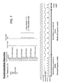
- FIG. 7 a block diagram illustrates an exemplary synchronization operation in accordance with one or more preferred aspects of the present invention.
- processors SPE 1 and SPE 2 are operating in synchronization. While no lock is present (cycles 1 - 5 ), SPE 2 operates at its normal, initial frequency with a loop count of zero.
- SPE 1 locks data that must remain unchanged by other processors, e.g. SPE 2
- SPE 2 may not access the data, and because SPE 2 must operate on the locked data before moving on to another task, SPE 2 enters into a loop (cycle 6 ), adding one to the loop count.
- cycles 7 and 8 SPE 2 is still in a wait loop, but as the loop count of 1 is below the threshold value of 2, the frequency of SPE 2 remains unchanged.
- SPE 2 loads the lock value, compares the lock value, and branches to the wait loop again (cycle 9 ) because the lock value for the data indicates that a lock on the data is not available to SPE 2 .
- the loop count increases by 1, thus equaling 2 , the threshold value, causing the frequency to be reduced to half (ratio of 1 ⁇ 2).
- the wait period is generally a significant number of clock cycles, it has been shortened here for purposes of illustration.
- the loop count increases and the frequency remains reduced to half.
- the data become available, SPE 2 does not take the loop branch, and the loop counter is reset to zero. With the loop count below the threshold value, the frequency is returned to normal for cycles 18 and 19 .
- the frequency is considered normal when it has a clock enable ratio of 1:1 to the initial frequency, considering that the initial frequency may vary based on processing and environmental circumstances.
- the initial frequency is considered normal insofar as the processor SPE 2 presumably would operate at its fastest, optimal or recommended frequency when performing productive processing under normal circumstances.
- each given processor 110 may have a different frequency that is considered normal for the given processor 110 , what is a normal frequency for SPE 1 may differ from what is a normal frequency for SPE 2 .
- what is normal for SPE 1 under a first set of conditions may not be normal for SPE 1 under a second set of conditions.
- the reference frequency at which the select processor 110 again may operate defaults to the initial frequency at which the select processor 110 was operating before having its frequency reduced.
- the increase in frequency likewise may be progressive and need not immediately return to the initial frequency.
- the frequency increase may cause the select processor 110 to operate at a frequency higher than the initial frequency, if conditions and configurations allow it. Power savings considerations may warrant a progressive increase in the frequency, such as available battery power, relative importance of the processing being performed, and dependency on data to be computed by another waiting processor. For instance, if processor 110 B waits on processor 110 A, and meanwhile processor 110 D is waiting on processor 110 C, and the result of processor 110 B is destined for processor 110 D, even once processor 110 B stops waiting, it may not be useful to fully increase the frequency of processor 110 B if processor 110 D is waiting still and not ready to receive the result from processor 110 B.
- the present invention has been described with reference to various preferred embodiments, it should be clear to a person of ordinary skill in the art that the present invention may be implemented using other means of tracking the pendency of waiting periods of waiting processors.
- the invention does not require the use of a loop count to determine the duration of the waiting period. Any appropriate means may be used, such as delay times, periods of unavailability of the specific data, etc.
- the loop count monitor may be replaced more broadly with a waiting period monitor operable to measure the waiting period and track waiting period data.
- the invention may include tracking waiting data relating to waiting processor waiting for data to become available; analyzing the waiting data to create a waiting data analysis outcome; and determining the frequency of the waiting processor in view of the waiting data analysis outcome.
- the availability monitor 216 may track the availability of data. When a lock is put on a data block, the lock may be registered with the availability monitor 216 . Any data requests would check with the availability monitor 216 to learn whether the desired data are available. If not, the frequency of the processor requiring the data may be reduced until the desired data become available, at which point the availability monitor 216 notifies the waiting processor and the frequency of the waiting processor is restored to normal.
- the multi-processor system 100 may be implemented as a single-chip solution operable for stand-alone and/or distributed processing of media-rich applications, such as game systems, home terminals, PC systems, server systems and workstations.
- media-rich applications such as game systems, home terminals, PC systems, server systems and workstations.
- real-time computing may be a necessity.
- one or more of networking image decompression, 3D computer graphics, audio generation, network communications, physical simulation, and artificial intelligence processes have to be executed quickly enough to provide the user with the illusion of a real-time experience.
- each processor in the multi-processor system 100 must complete tasks in a short and predictable time.
- all processors of a multi-processing computer system 100 are constructed from a common computing module (or cell).
- This common computing module has a consistent structure and preferably employs the same instruction set architecture.
- the multi-processing computer system 100 can be formed of one or more clients, servers, PCs, mobile computers, game machines, PDAs, set top boxes, appliances, digital televisions and other devices using computer processors.
- a plurality of the computer systems 100 also may be members of a network if desired.
- the consistent modular structure enables efficient, high speed processing of applications and data by the multi-processing computer system, and if a network is employed, the rapid transmission of applications and data over the network.
- This structure also simplifies the building of members of the network of various sizes and processing power and the preparation of applications for processing by these members.
- FIG. 8 to FIG. 10 A description of a preferred computer architecture for a multi-processor system is provided in FIG. 8 to FIG. 10 that is suitable for carrying out one or more of the features discussed herein.
- a preferred structure of a basic processing module is shown as a broadband engine (BE) 1000 .
- the BE 1000 comprises an I/O interface 1300 , a POWER processing element (PPE) 1200 , and a plurality of synergistic processing elements 1100 , namely, synergistic processing element 1100 A, synergistic processing element 1100 B, synergistic processing element 1100 C, and synergistic processing element 1100 D.
- a local (or internal) BE bus 1500 transmits data and applications among the PPE 1200 , the synergistic processing elements 1100 , and a memory interface 1400 .
- the local BE bus 1500 can have, e.g., a conventional architecture or can be implemented as a packet-switched network. If implemented as a packet switch network, while requiring more hardware, increases the available bandwidth.
- the BE 1000 can be constructed using various methods for implementing digital logic.
- the BE 1000 preferably is constructed, however, as a single integrated circuit employing a complementary metal oxide semiconductor (CMOS) on a silicon substrate.
- CMOS complementary metal oxide semiconductor
- Alternative materials for substrates include gallium arsinide, gallium aluminum arsinide and other so-called III-B compounds employing a wide variety of dopants.
- the BE 1000 also may be implemented using superconducting material, e.g., rapid single-flux-quantum (RSFQ) logic.
- RSFQ rapid single-flux-quantum
- the BE 1000 is closely associated with a shared (main) memory 1600 through a high bandwidth memory connection 1700 .
- the memory 1600 preferably is a dynamic random access memory (DRAM)
- the memory 1600 could be implemented using other means, e.g., as a static random access memory (SRAM), a magnetic random access memory (MRAM), an optical memory, a holographic memory, etc.
- the PPE 1200 and the synergistic processing elements 1100 are preferably each coupled to a memory flow controller (MFC) including direct memory access DMA functionality, which in combination with the memory interface 1400 , facilitate the transfer of data between the DRAM 1600 and the synergistic processing elements 1100 and the PPE 1200 of the BE 1000 .
- MFC memory flow controller
- the DMAC and/or the memory interface 1400 may be integrally or separately disposed with respect to the synergistic processing elements 1100 and the PPE 1200 .
- the DMAC function and/or the memory interface 1400 function may be integral with one or more (preferably all) of the synergistic processing elements 1100 and the PPE 1200 .
- the DRAM 1600 may be integrally or separately disposed with respect to the BE 1000 .
- the DRAM 1600 may be disposed off-chip as is implied by the illustration shown or the DRAM 1600 may be disposed on-chip in an integrated fashion.
- the PPE 1200 can be, e.g., a standard processor capable of stand-alone processing of data and applications.
- the PPE 1200 preferably schedules and orchestrates the processing of data and applications by the synergistic processing elements.
- the synergistic processing elements preferably are single instruction, multiple data (SIMD) processors. Under the control of the PPE 1200 , the synergistic processing elements perform the processing of these data and applications in a parallel and independent manner.
- the PPE 1200 is preferably implemented using a PowerPC core, which is a microprocessor architecture that employs reduced instruction-set computing (RISC) technique. RISC performs more complex instructions using combinations of simple instructions. Thus, the timing for the processor may be based on simpler and faster operations, enabling the microprocessor to perform more instructions for a given clock speed.
- RISC reduced instruction-set computing
- the PPE 1200 may be implemented by one of the synergistic processing elements 1100 taking on the role of a main processing unit that schedules and orchestrates the processing of data and applications by the synergistic processing elements 1100 . Further, there may be more than one PPE implemented within the broadband engine 1000 .
- the number of BEs 1000 employed by a particular computer system is based upon the processing power required by that system. For example, a server may employ four BEs 1000 , a workstation may employ two BEs 1000 and a PDA may employ one BE 1000 .
- the number of synergistic processing elements 1100 of a BE 1000 assigned to processing a particular software cell depends upon the complexity and magnitude of the programs and data within the cell.
- the SPE 1100 architecture preferably fills a void between general-purpose processors (which are designed to achieve high average performance on a broad set of applications) and special-purpose processors (which are designed to achieve high performance on a single application).
- the SPE 1100 is designed to achieve high performance on game applications, media applications, broadband systems, etc., and to provide a high degree of control to programmers of real-time applications.
- SPE 1100 Some capabilities of the SPE 1100 include graphics geometry pipelines, surface subdivision, Fast Fourier Transforms, image processing keywords, stream processing, MPEG encoding/decoding, encryption, decryption, device driver extensions, modeling, game physics, content creation, and audio synthesis and processing.
- the synergistic processing element 1100 includes two basic functional units, namely a streaming processing unit (SPU) 1120 and a memory flow controller (MFC) 1140 .
- the SPU 1120 performs program execution, data manipulation, etc., while the MFC 1140 performs functions related to data transfers between the SPU 1120 and the DRAM 1600 of the system.
- the SPU 1120 includes a local memory 1121 , an instruction unit (IU) 1122 , registers 1123 , one ore more floating point execution stages 1124 and one or more fixed point execution stages 1125 .
- the local memory 1121 is preferably implemented using single-ported random access memory, such as an SRAM. Whereas most processors reduce latency to memory by employing caches, the SPU 1120 implements the relatively small local memory 1121 rather than a cache. Indeed, in order to provide consistent and predictable memory access latency for programmers of real-time applications (and other applications as mentioned herein) a cache memory architecture within the SPU 1120 is not preferred. The cache hit/miss characteristics of a cache memory results in volatile memory access times, varying from a few cycles to a few hundred cycles.
- Latency hiding may be achieved in the local memory SRAM 1121 by overlapping DMA transfers with data computation. This provides a high degree of control for the programming of real-time applications. As the latency and instruction overhead associated with DMA transfers exceeds that of the latency of servicing a cache miss, the SRAM local memory approach achieves an advantage when the DMA transfer size is sufficiently large and is sufficiently predictable (e.g., a DMA command can be issued before data is needed).
- a program running on a given one of the synergistic processing elements 1100 references the associated local memory 1121 using a local address. However, each location of the local memory 1121 is also assigned a real address (RA) within the memory map of the overall system. This allows Privilege Software to map a local memory 1121 into the Effective Address (EA) of a process to facilitate DMA transfers between one local memory 1121 and another local memory 1121 .
- the PPE 1200 can also directly access the local memory 1121 using an effective address.
- the local memory 1121 contains 556 kilobytes of storage, and the capacity of registers 1123 is 128 ⁇ 128 bits.
- the SPU 1120 is preferably implemented using a processing pipeline, in which logic instructions are processed in a pipelined fashion.
- the pipeline may be divided into any number of stages at which instructions are processed, the pipeline generally comprises fetching one or more instructions, decoding the instructions, checking for dependencies among the instructions, issuing the instructions, and executing the instructions.
- the IU 1122 includes an instruction buffer, instruction decode circuitry, dependency check circuitry, and instruction issue circuitry.
- the instruction buffer preferably includes a plurality of registers that are coupled to the local memory 1121 and operable to temporarily store instructions as they are fetched.
- the instruction buffer preferably operates such that all the instructions leave the registers as a group, i.e., substantially simultaneously.
- the instruction buffer may be of any size, it is preferred that it is of a size not larger than about two or three registers.
- the decode circuitry breaks down the instructions and generates logical micro-operations that perform the function of the corresponding instruction.
- the logical micro-operations may specify arithmetic and logical operations, load and store operations to the local memory 1121 , register source operands and/or immediate data operands.
- the decode circuitry may also indicate which resources the instruction uses, such as target register addresses, structural resources, function units and/or busses.
- the decode circuitry may also supply information indicating the instruction pipeline stages in which the resources are required.
- the instruction decode circuitry is preferably operable to substantially simultaneously decode a number of instructions equal to the number of registers of the instruction buffer.
- the dependency check circuitry includes digital logic that performs testing to determine whether the operands of given instruction are dependent on the operands of other instructions in the pipeline. If so, then the given instruction should not be executed until such other operands are updated (e.g., by permitting the other instructions to complete execution). It is preferred that the dependency check circuitry determines dependencies of multiple instructions dispatched from the decode circuitry simultaneously.
- the instruction issue circuitry is operable to issue the instructions to the floating point execution stages 1124 and/or the fixed point execution stages 1125 .
- the registers 1123 are preferably implemented as a relatively large unified register file, such as a 128-entry register file. This allows for deeply pipelined high-frequency implementations without requiring register renaming to avoid register starvation. Renaming hardware typically consumes a significant fraction of the area and power in a processing system. Consequently, advantageous operation may be achieved when latencies are covered by software loop unrolling or other interleaving techniques.
- the SPU 1120 is of a superscalar architecture, such that more than one instruction is issued per clock cycle.
- the SPU 1120 preferably operates as a superscalar to a degree corresponding to the number of simultaneous instruction dispatches from the instruction buffer, such as between 2 and 3 (meaning that two or three instructions are issued each clock cycle).
- a greater or lesser number of floating point execution stages 1124 and fixed point execution stages 1125 may be employed.
- the floating point execution stages 1124 operate at a speed of 32 billion floating point operations per second (32 GFLOPS), and the fixed point execution stages 1125 operate at a speed of 32 billion operations per second (32 GOPS).
- the MFC 1140 preferably includes a direct memory access controller (DMAC) 1141 , a memory management unit (MMU) 1142 , and a bus interface unit (BIU) 1143 .
- DMAC direct memory access controller
- MMU memory management unit
- BIU bus interface unit
- the MFC 1140 preferably runs at half frequency (half speed) as compared with the SPU 1120 and the bus 1500 to meet low power dissipation design objectives.
- the MFC 1140 is operable to handle data and instructions coming into the SPE 1100 from the bus 1500 , provides address translation for the DMAC, and snoop-operations for data coherency.
- the BIU 1143 provides an interface between the bus 1500 and the MMU 1142 and DMAC 1141 .
- the SPE 1100 including the SPU 1120 and the MFC 1140
- the DMAC 1141 are connected physically and/or logically to the bus 1500 .
- the MMU 1142 is preferably operable to translate effective addresses (taken from DMA commands) into real addresses for memory access.
- the MMU 1142 may translate the higher order bits of the effective address into real address bits.
- the lower-order address bits are preferably untranslatable and are considered both logical and physical for use to form the real address and request access to memory.
- the MMU 1142 may be implemented based on a 64-bit memory management model, and may provide 2 64 bytes of effective address space with 4K-, 64K-, 1M-, and 16M-byte page sizes and 256 MB segment sizes.
- the MMU 1142 is operable to support up to 2 65 bytes of virtual memory, and 2 42 bytes (4 TeraBytes) of physical memory for DMA commands.
- the hardware of the MMU 1142 may include an 8-entry, fully associative SLB, a 256-entry, 4 way set associative TLB, and a 4 ⁇ 4 Replacement Management Table (RMT) for the TLB—used for hardware TLB miss handling.
- RMT Replacement Management Table
- the DMAC 1141 is preferably operable to manage DMA commands from the SPU 1120 and one or more other devices such as the PPE 1200 and/or the other SPUs.
- DMA commands There may be three categories of DMA commands: Put commands, which operate to move data from the local memory 1121 to the shared memory 1600 ; Get commands, which operate to move data into the local memory 1121 from the shared memory 1600 ; and Storage Control commands, which include SLI commands and synchronization commands.
- the synchronization commands may include atomic commands, send signal commands, and dedicated barrier commands.
- the MMU 1142 translates the effective address into a real address and the real address is forwarded to the BIU 1143 .
- the SPU 1120 preferably uses a channel interface and data interface to communicate (send DMA commands, status, etc.) with an interface within the DMAC 1141 .
- the SPU 1120 dispatches DMA commands through the channel interface to a DMA queue in the DMAC 1141 . Once a DMA command is in the DMA queue, it is handled by issue and completion logic within the DMAC 1141 . When all bus transactions for a DMA command are finished, a completion signal is sent back to the SPU 1120 over the channel interface.
- the PPE 1200 includes two basic functional units, the PPE core 1220 and the memory flow controller (MFC) 1240 .
- the PPE core 1220 performs program execution, data manipulation, multi-processor management functions, etc., while the MFC 1240 performs functions related to data transfers between the PPE core 1220 and the memory space of the system 100 .
- the PPE core 1220 may include an L1 cache 1221 , an instruction unit 1222 , registers 1223 , one or more floating point execution stages 1224 and one or more fixed point execution stages 1225 .
- the L1 cache 1221 provides data caching functionality for data received from the shared memory 1600 , the processors 1100 , or other portions of the memory space through the MFC 1240 .
- the instruction unit 1222 is preferably implemented as an instruction pipeline with many stages, including fetching, decoding, dependency checking, issuing, etc.
- the PPE core 1220 is also preferably of a superscalar configuration, whereby more than one instruction is issued from the instruction unit 1222 per clock cycle.
- the floating point execution stages 1224 and the fixed point execution stages 1225 include a plurality of stages in a pipeline configuration. Depending upon the required processing power, a greater or lesser number of floating point execution stages 1224 and fixed point execution stages 1225 may be employed.
- the MFC 1240 includes a bus interface unit (BIU) 1241 , an L2 cache memory 1242 , a non-cachable unit (NCU) 1243 , a core interface unit (CIU) 1244 , and a memory management unit (MMU) 1245 .
- BIU bus interface unit
- NCU non-cachable unit
- CCU core interface unit
- MMU memory management unit
- the BIU 1241 provides an interface between the bus 1500 and the L2 cache 1242 and NCU 1243 logic blocks. To this end, the BIU 1241 may act as a Master as well as a Slave device on the bus 1500 in order to perform fully coherent memory operations. As a Master device it may source load/store requests to the bus 1500 for service on behalf of the L2 cache 1242 and the NCU 1243 . The BIU 1241 may also implement a flow control mechanism for commands which limits the total number of commands that can be sent to the bus 1500 .
- the data operations on the bus 1500 may be designed to take eight beats and, therefore, the BIU 1241 is preferably designed around 128 byte cache-lines and the coherency and synchronization granularity is 128 KB.
- the L2 cache memory 1242 (with supporting hardware logic) is preferably designed to cache 512 KB of data.
- the L2 cache 1242 may handle cacheable loads/stores, data pre-fetches, instruction fetches, instruction pre-fetches, cache operations, and barrier operations.
- the L2 cache 1242 is preferably an 8-way set associative system.
- the L2 cache 1242 may include six reload queues matching six (6) castout queues (e.g., six RC machines), and eight (64-byte wide) store queues.
- the L2 cache 1242 may operate to provide a backup copy of some or all of the data in the L1 cache 1221 .
- this is useful in restoring state(s) when processing nodes are hot-swapped.
- This configuration also permits the L1 cache 1221 to operate more quickly with fewer ports, and permits faster cache-to-cache transfers (because the requests may stop at the L2 cache 1242 ).
- This configuration also provides a mechanism for passing cache coherency management to the L2 cache memory 1242 .
- the NCU 1243 interfaces with the CIU 1244 , the L2 cache memory 1242 , and the BIU 1241 and generally functions as a queuing/buffering circuit for non-cacheable operations between the PPE core 1220 and the memory system.
- the NCU 1243 preferably handles all communications with the PPE core 1220 that are not handled by the L2 cache 1242 , such as cache-inhibited load/stores, barrier operations, and cache coherency operations.
- the NCU 1243 is preferably run at half speed to meet the aforementioned power dissipation objectives.
- the CIU 1244 is disposed on the boundary of the MFC 1240 and the PPE core 1220 and acts as a routing, arbitration, and flow control point for requests coming from the execution stages 1224 , 1225 , the instruction unit 1222 , and the MMU unit 1245 and going to the L2 cache 1242 and the NCU 1243 .
- the PPE core 1220 and the MMU 1245 preferably run at full speed, while the L2 cache 1242 and the NCU 1243 are operable for a 2:1 speed ratio.
- a frequency boundary exists in the CIU 1244 and one of its functions is to properly handle the frequency crossing as it forwards requests and reloads data between the two frequency domains.
- the CIU 1244 is comprised of three functional blocks: a load unit, a store unit, and reload unit.
- a data pre-fetch function is performed by the CIU 1244 and is preferably a functional part of the load unit.
- the CIU 1244 is preferably operable to: (i) accept load and store requests from the PPE core 1220 and the MMU 1245 ; (ii) convert the requests from full speed clock frequency to half speed (a 2:1 clock frequency conversion); (iii) route cachable requests to the L2 cache 1242 , and route non-cachable requests to the NCU 1243 ; (iv) arbitrate fairly between the requests to the L2 cache 1242 and the NCU 1243 ; (v) provide flow control over the dispatch to the L2 cache 1242 and the NCU 1243 so that the requests are received in a target window and overflow is avoided; (vi) accept load return data and route it to the execution stages 1224 , 1225 , the instruction unit 1222 , or the MMU 1245
- the MMU 1245 preferably provides address translation for the PPE core 440 A, such as by way of a second level address translation facility.
- a first level of translation is preferably provided in the PPE core 1220 by separate instruction and data ERAT (effective to real address translation) arrays that may be much smaller and faster than the MMU 1245 .
- the PPE 1200 operates at 4-6 GHz, 10F04, with a 64-bit implementation.
- the registers are preferably 64 bits long (although one or more special purpose registers may be smaller) and effective addresses are 64 bits long.
- the instruction unit 1222 , registers 1223 and execution stages 1224 and 1225 are preferably implemented using PowerPC technology to achieve the (RISC) computing technique.
- the methods and apparatus described above may be achieved utilizing suitable hardware, such as that illustrated in the figures.
- suitable hardware such as that illustrated in the figures.
- Such hardware may be implemented utilizing any of the known technologies, such as standard digital circuitry, any of the known processors that are operable to execute software and/or firmware programs, one or more programmable digital devices or systems, such as programmable read only memories (PROMs), programmable array logic devices (PALs), etc.
- PROMs programmable read only memories
- PALs programmable array logic devices
- the apparatus illustrated in the figures are shown as being partitioned into certain functional blocks, such blocks may be implemented by way of separate circuitry and/or combined into one or more functional units.
- the various aspects of the invention may be implemented by way of software and/or firmware program(s) that may be stored on suitable storage medium or media (such as floppy disk(s), memory chip(s), etc.) for transportability and/or distribution.
Abstract
Description
Claims (27)
Priority Applications (3)
| Application Number | Priority Date | Filing Date | Title |
|---|---|---|---|
| US11/525,306 US7882379B2 (en) | 2006-09-22 | 2006-09-22 | Power consumption reduction in a multiprocessor system |
| JP2007205861A JP2008077640A (en) | 2006-09-22 | 2007-08-07 | Method and device for power consumption reduction in multiprocessor system |
| US12/974,124 US9058164B2 (en) | 2006-09-22 | 2010-12-21 | Power consumption reduction in a multiprocessor system |
Applications Claiming Priority (1)
| Application Number | Priority Date | Filing Date | Title |
|---|---|---|---|
| US11/525,306 US7882379B2 (en) | 2006-09-22 | 2006-09-22 | Power consumption reduction in a multiprocessor system |
Related Child Applications (1)
| Application Number | Title | Priority Date | Filing Date |
|---|---|---|---|
| US12/974,124 Continuation US9058164B2 (en) | 2006-09-22 | 2010-12-21 | Power consumption reduction in a multiprocessor system |
Publications (2)
| Publication Number | Publication Date |
|---|---|
| US20080077815A1 US20080077815A1 (en) | 2008-03-27 |
| US7882379B2 true US7882379B2 (en) | 2011-02-01 |
Family
ID=39226434
Family Applications (2)
| Application Number | Title | Priority Date | Filing Date |
|---|---|---|---|
| US11/525,306 Active 2029-04-09 US7882379B2 (en) | 2006-09-22 | 2006-09-22 | Power consumption reduction in a multiprocessor system |
| US12/974,124 Active 2028-07-19 US9058164B2 (en) | 2006-09-22 | 2010-12-21 | Power consumption reduction in a multiprocessor system |
Family Applications After (1)
| Application Number | Title | Priority Date | Filing Date |
|---|---|---|---|
| US12/974,124 Active 2028-07-19 US9058164B2 (en) | 2006-09-22 | 2010-12-21 | Power consumption reduction in a multiprocessor system |
Country Status (2)
| Country | Link |
|---|---|
| US (2) | US7882379B2 (en) |
| JP (1) | JP2008077640A (en) |
Cited By (14)
| Publication number | Priority date | Publication date | Assignee | Title |
|---|---|---|---|---|
| US20100313041A1 (en) * | 2009-06-08 | 2010-12-09 | Fujitsu Limited | Power management circuit, power management method and power management program |
| US20110221724A1 (en) * | 2010-03-12 | 2011-09-15 | Semiconductor Energy Laboratory Co., Ltd. | Method for driving input circuit and method for driving display device |
| US20120167107A1 (en) * | 2009-05-13 | 2012-06-28 | De Cesare Josh P | Power Managed Lock Optimization |
| US20120246652A1 (en) * | 2011-03-22 | 2012-09-27 | International Business Machines Corporation | Processor Management Via Thread Status |
| US8605059B2 (en) | 2010-07-02 | 2013-12-10 | Semiconductor Energy Laboratory Co., Ltd. | Input/output device and driving method thereof |
| US8908406B2 (en) | 2011-06-09 | 2014-12-09 | Semiconductor Energy Laboratory Co., Ltd. | Cache memory and method for driving the same |
| US8953354B2 (en) | 2011-06-09 | 2015-02-10 | Semiconductor Energy Laboratory Co., Ltd. | Semiconductor memory device and method of driving semiconductor memory device |
| US9135182B2 (en) | 2012-06-01 | 2015-09-15 | Semiconductor Energy Laboratory Co., Ltd. | Central processing unit and driving method thereof |
| US9442559B2 (en) | 2013-03-14 | 2016-09-13 | Intel Corporation | Exploiting process variation in a multicore processor |
| US9626889B2 (en) | 2012-09-24 | 2017-04-18 | Semiconductor Energy Laboratory Co., Ltd. | Method and program for driving information processing device |
| US20180074566A1 (en) * | 2016-09-12 | 2018-03-15 | Canon Kabushiki Kaisha | Information processing apparatus, method for controlling the same, and non-transitory computer-readable storage medium |
| US10042731B2 (en) | 2013-11-11 | 2018-08-07 | Samsung Electronics Co., Ltd. | System-on-chip having a symmetric multi-processor and method of determining a maximum operating clock frequency for the same |
| US10073718B2 (en) | 2016-01-15 | 2018-09-11 | Intel Corporation | Systems, methods and devices for determining work placement on processor cores |
| US10496149B2 (en) | 2015-08-31 | 2019-12-03 | Samsung Electronics Co., Ltd. | Method of operating CPU and method of operating system having the CPU |
Families Citing this family (20)
| Publication number | Priority date | Publication date | Assignee | Title |
|---|---|---|---|---|
| US8132030B2 (en) * | 2006-06-27 | 2012-03-06 | Koninklijke Philips Electronics N.V. | Device and a method for managing power consumption of a plurality of data processing units |
| TW200837767A (en) * | 2007-03-09 | 2008-09-16 | Usbest Technology Inc | Data storing device and method capable of reducing power consumption there of |
| US8214662B2 (en) * | 2007-04-09 | 2012-07-03 | Panasonic Corporation | Multiprocessor control unit, control method performed by the same, and integrated circuit |
| CN101373434B (en) * | 2007-08-22 | 2012-01-25 | 国际商业机器公司 | Method and system for rapidly loading and operating program mapping in multiprocessor system |
| JP4548505B2 (en) * | 2008-04-16 | 2010-09-22 | ソニー株式会社 | Information processing apparatus, information processing method, and computer program |
| US20090327656A1 (en) * | 2008-05-16 | 2009-12-31 | Dan Baum | Efficiency-based determination of operational characteristics |
| US8261117B2 (en) * | 2008-09-11 | 2012-09-04 | International Business Machines Corporation | Virtualization in a multi-core processor (MCP) |
| US8732716B2 (en) | 2008-09-30 | 2014-05-20 | International Business Machines Corporation | Virtualization across physical partitions of a multi-core processor (MCP) |
| JP2010113574A (en) * | 2008-11-07 | 2010-05-20 | Panasonic Corp | Resource exclusive control method in multiprocessor, exclusive control system and technology associated with the same |
| WO2012095982A1 (en) * | 2011-01-13 | 2012-07-19 | 富士通株式会社 | Multi-core processor system and scheduling method |
| US8819347B2 (en) * | 2011-05-09 | 2014-08-26 | Bae Systems Information And Electronic Systems Integration Inc. | Mailbox data communications |
| US9086883B2 (en) * | 2011-06-10 | 2015-07-21 | Qualcomm Incorporated | System and apparatus for consolidated dynamic frequency/voltage control |
| US8713262B2 (en) * | 2011-09-02 | 2014-04-29 | Nvidia Corporation | Managing a spinlock indicative of exclusive access to a system resource |
| JP5786641B2 (en) | 2011-10-25 | 2015-09-30 | 富士通株式会社 | Control method of portable terminal device, control program, and portable terminal device |
| JP5776789B2 (en) * | 2011-11-15 | 2015-09-09 | 富士通株式会社 | Power control apparatus, electronic computer, and power control method |
| JP6070321B2 (en) * | 2013-03-21 | 2017-02-01 | 富士通株式会社 | Portable information terminal, control method, control program |
| JP6221792B2 (en) * | 2014-02-05 | 2017-11-01 | 富士通株式会社 | Information processing apparatus, information processing system, and information processing system control method |
| US10095434B2 (en) | 2015-01-02 | 2018-10-09 | Reservoir Labs, Inc. | Systems and methods for efficient determination of task dependences after loop tiling |
| US20180314289A1 (en) * | 2017-04-28 | 2018-11-01 | Intel Corporation | Modifying an operating frequency in a processor |
| CN114465820A (en) * | 2022-03-31 | 2022-05-10 | 京东方科技集团股份有限公司 | Data encryption method, data encryption device, electronic device, program, and medium |
Citations (18)
| Publication number | Priority date | Publication date | Assignee | Title |
|---|---|---|---|---|
| US5724591A (en) * | 1995-01-27 | 1998-03-03 | Hitachi, Ltd. | Multiprocessor system with reduced power mode and improved variation of power demand |
| US5768550A (en) * | 1995-11-21 | 1998-06-16 | International Business Machines Corporation | Bus interface logic system |
| US5774704A (en) * | 1996-07-29 | 1998-06-30 | Silicon Graphics, Inc. | Apparatus and method for dynamic central processing unit clock adjustment |
| US6006299A (en) * | 1994-03-01 | 1999-12-21 | Intel Corporation | Apparatus and method for caching lock conditions in a multi-processor system |
| US6137804A (en) * | 1997-12-02 | 2000-10-24 | International Business Machines Corporation | System and method for automatic retry of transmit, independent of a host processor, after an underrun occurs in a LAN |
| US6526491B2 (en) | 2001-03-22 | 2003-02-25 | Sony Corporation Entertainment Inc. | Memory protection system and method for computer architecture for broadband networks |
| US20030120963A1 (en) * | 2001-12-20 | 2003-06-26 | Jahnke Steven R. | Variable clocking in an embedded symmetric multiprocessor system |
| US6684342B1 (en) * | 2000-06-22 | 2004-01-27 | Ubicom, Inc. | Apparatus and method of dynamic and deterministic changes in clock frequency for lower power consumption while maintaining fast interrupt handling |
| US20040098631A1 (en) * | 2002-11-20 | 2004-05-20 | Terrell James Richard | System clock power management for chips with multiple processing modules |
| US6745335B1 (en) * | 1999-10-12 | 2004-06-01 | Nec Corporation | Power consumption control of multiprocessor system using separate timers for monitoring processor load rise and drop |
| US6874080B2 (en) * | 2001-11-19 | 2005-03-29 | Intel Corporation | Context processing by substantially simultaneously selecting address and instruction of different contexts |
| US6928566B2 (en) * | 2001-01-18 | 2005-08-09 | Renesas Technology Corp. | Multiprocessor system controlling frequency of clock input to processor according to ratio of processing times of processors, and method thereof |
| US6990598B2 (en) * | 2001-03-21 | 2006-01-24 | Gallitzin Allegheny Llc | Low power reconfigurable systems and methods |
| US7065614B1 (en) * | 2003-06-20 | 2006-06-20 | Unisys Corporation | System and method for maintaining memory coherency within a multi-processor data processing system |
| US20070067675A1 (en) * | 2005-09-21 | 2007-03-22 | Cisco Technology, Inc. | Method and system for managing failure information |
| US7225277B2 (en) * | 2003-09-04 | 2007-05-29 | International Business Machines Corporation | Proxy direct memory access |
| US7249270B2 (en) * | 2004-05-26 | 2007-07-24 | Arm Limited | Method and apparatus for placing at least one processor into a power saving mode when another processor has access to a shared resource and exiting the power saving mode upon notification that the shared resource is no longer required by the other processor |
| US20080270711A1 (en) * | 2007-04-30 | 2008-10-30 | Electronics And Telecommunications Research Institute | Method and apparatus for data transmission between processors using memory remapping |
Family Cites Families (13)
| Publication number | Priority date | Publication date | Assignee | Title |
|---|---|---|---|---|
| US6192479B1 (en) * | 1995-01-19 | 2001-02-20 | Texas Instruments Incorporated | Data processing with progressive, adaptive, CPU-driven power management |
| JPH11143573A (en) * | 1997-11-10 | 1999-05-28 | Fujitsu Ltd | Clock supplying method and information processor |
| US6233690B1 (en) * | 1998-09-17 | 2001-05-15 | Intel Corporation | Mechanism for saving power on long latency stalls |
| US6446215B1 (en) * | 1999-08-20 | 2002-09-03 | Advanced Micro Devices, Inc. | Method and apparatus for controlling power management state transitions between devices connected via a clock forwarded interface |
| EP1679590B1 (en) * | 2001-01-31 | 2011-03-23 | Renesas Electronics Corporation | Data processing system |
| DE20302484U1 (en) * | 2003-01-23 | 2003-09-04 | Elitegroup Comp Systems Co | Control panel for setting the operating frequency of a computer and displaying system information |
| US7028197B2 (en) * | 2003-04-22 | 2006-04-11 | Lsi Logic Corporation | System and method for electrical power management in a data processing system using registers to reflect current operating conditions |
| US7206950B2 (en) * | 2004-06-16 | 2007-04-17 | Matsushita Electric Industrial Co., Ltd. | Processor system, instruction sequence optimization device, and instruction sequence optimization program |
| US8316048B2 (en) * | 2004-08-17 | 2012-11-20 | Hewlett-Packard Development Company, L.P. | Method and apparatus for managing a data structure for multi-processor access |
| JP2008518310A (en) * | 2004-10-25 | 2008-05-29 | ローベルト ボッシュ ゲゼルシャフト ミット ベシュレンクテル ハフツング | Method and apparatus for monitoring memory units in a multiprocessor system |
| US20070294559A1 (en) * | 2004-10-25 | 2007-12-20 | Thomas Kottke | Method and Device for Delaying Access to Data and/or Instructions of a Multiprocessor System |
| US20060206743A1 (en) * | 2005-03-08 | 2006-09-14 | Hui-Huang Chang | Computer system having a clock controller for controlling an operating clock inputted into a no-wait-state microprocessor and method thereof |
| US7055614B1 (en) | 2005-03-10 | 2006-06-06 | Victaulic Company | Torque plate for sprinkler head |
-
2006
- 2006-09-22 US US11/525,306 patent/US7882379B2/en active Active
-
2007
- 2007-08-07 JP JP2007205861A patent/JP2008077640A/en active Pending
-
2010
- 2010-12-21 US US12/974,124 patent/US9058164B2/en active Active
Patent Citations (18)
| Publication number | Priority date | Publication date | Assignee | Title |
|---|---|---|---|---|
| US6006299A (en) * | 1994-03-01 | 1999-12-21 | Intel Corporation | Apparatus and method for caching lock conditions in a multi-processor system |
| US5724591A (en) * | 1995-01-27 | 1998-03-03 | Hitachi, Ltd. | Multiprocessor system with reduced power mode and improved variation of power demand |
| US5768550A (en) * | 1995-11-21 | 1998-06-16 | International Business Machines Corporation | Bus interface logic system |
| US5774704A (en) * | 1996-07-29 | 1998-06-30 | Silicon Graphics, Inc. | Apparatus and method for dynamic central processing unit clock adjustment |
| US6137804A (en) * | 1997-12-02 | 2000-10-24 | International Business Machines Corporation | System and method for automatic retry of transmit, independent of a host processor, after an underrun occurs in a LAN |
| US6745335B1 (en) * | 1999-10-12 | 2004-06-01 | Nec Corporation | Power consumption control of multiprocessor system using separate timers for monitoring processor load rise and drop |
| US6684342B1 (en) * | 2000-06-22 | 2004-01-27 | Ubicom, Inc. | Apparatus and method of dynamic and deterministic changes in clock frequency for lower power consumption while maintaining fast interrupt handling |
| US6928566B2 (en) * | 2001-01-18 | 2005-08-09 | Renesas Technology Corp. | Multiprocessor system controlling frequency of clock input to processor according to ratio of processing times of processors, and method thereof |
| US6990598B2 (en) * | 2001-03-21 | 2006-01-24 | Gallitzin Allegheny Llc | Low power reconfigurable systems and methods |
| US6526491B2 (en) | 2001-03-22 | 2003-02-25 | Sony Corporation Entertainment Inc. | Memory protection system and method for computer architecture for broadband networks |
| US6874080B2 (en) * | 2001-11-19 | 2005-03-29 | Intel Corporation | Context processing by substantially simultaneously selecting address and instruction of different contexts |
| US20030120963A1 (en) * | 2001-12-20 | 2003-06-26 | Jahnke Steven R. | Variable clocking in an embedded symmetric multiprocessor system |
| US20040098631A1 (en) * | 2002-11-20 | 2004-05-20 | Terrell James Richard | System clock power management for chips with multiple processing modules |
| US7065614B1 (en) * | 2003-06-20 | 2006-06-20 | Unisys Corporation | System and method for maintaining memory coherency within a multi-processor data processing system |
| US7225277B2 (en) * | 2003-09-04 | 2007-05-29 | International Business Machines Corporation | Proxy direct memory access |
| US7249270B2 (en) * | 2004-05-26 | 2007-07-24 | Arm Limited | Method and apparatus for placing at least one processor into a power saving mode when another processor has access to a shared resource and exiting the power saving mode upon notification that the shared resource is no longer required by the other processor |
| US20070067675A1 (en) * | 2005-09-21 | 2007-03-22 | Cisco Technology, Inc. | Method and system for managing failure information |
| US20080270711A1 (en) * | 2007-04-30 | 2008-10-30 | Electronics And Telecommunications Research Institute | Method and apparatus for data transmission between processors using memory remapping |
Cited By (26)
| Publication number | Priority date | Publication date | Assignee | Title |
|---|---|---|---|---|
| US8332559B2 (en) * | 2009-05-13 | 2012-12-11 | Apple Inc. | Power managed lock optimization |
| US8578079B2 (en) | 2009-05-13 | 2013-11-05 | Apple Inc. | Power managed lock optimization |
| US20120167107A1 (en) * | 2009-05-13 | 2012-06-28 | De Cesare Josh P | Power Managed Lock Optimization |
| US20100313041A1 (en) * | 2009-06-08 | 2010-12-09 | Fujitsu Limited | Power management circuit, power management method and power management program |
| US8407507B2 (en) * | 2009-06-08 | 2013-03-26 | Fujitsu Limited | Power management circuit, power management method and power management program for controlling power supplied to functional blocks in integrated circuits |
| US20110221724A1 (en) * | 2010-03-12 | 2011-09-15 | Semiconductor Energy Laboratory Co., Ltd. | Method for driving input circuit and method for driving display device |
| US9971440B2 (en) | 2010-03-12 | 2018-05-15 | Semiconductor Energy Laboratory Co., Ltd. | Method for driving circuit and method for driving display device |
| US8605059B2 (en) | 2010-07-02 | 2013-12-10 | Semiconductor Energy Laboratory Co., Ltd. | Input/output device and driving method thereof |
| US9886077B2 (en) | 2011-03-22 | 2018-02-06 | International Business Machines Corporation | Processor management via thread status |
| US20120246652A1 (en) * | 2011-03-22 | 2012-09-27 | International Business Machines Corporation | Processor Management Via Thread Status |
| US9354926B2 (en) * | 2011-03-22 | 2016-05-31 | International Business Machines Corporation | Processor management via thread status |
| US11157061B2 (en) | 2011-03-22 | 2021-10-26 | International Business Machines Corporation | Processor management via thread status |
| US8908406B2 (en) | 2011-06-09 | 2014-12-09 | Semiconductor Energy Laboratory Co., Ltd. | Cache memory and method for driving the same |
| US8953354B2 (en) | 2011-06-09 | 2015-02-10 | Semiconductor Energy Laboratory Co., Ltd. | Semiconductor memory device and method of driving semiconductor memory device |
| US9135182B2 (en) | 2012-06-01 | 2015-09-15 | Semiconductor Energy Laboratory Co., Ltd. | Central processing unit and driving method thereof |
| US9626889B2 (en) | 2012-09-24 | 2017-04-18 | Semiconductor Energy Laboratory Co., Ltd. | Method and program for driving information processing device |
| US9933893B2 (en) | 2012-09-24 | 2018-04-03 | Semiconductor Energy Laboratory Co., Ltd. | Method and program for driving information processing device |
| US9442559B2 (en) | 2013-03-14 | 2016-09-13 | Intel Corporation | Exploiting process variation in a multicore processor |
| US10042731B2 (en) | 2013-11-11 | 2018-08-07 | Samsung Electronics Co., Ltd. | System-on-chip having a symmetric multi-processor and method of determining a maximum operating clock frequency for the same |
| US10496149B2 (en) | 2015-08-31 | 2019-12-03 | Samsung Electronics Co., Ltd. | Method of operating CPU and method of operating system having the CPU |
| US10073718B2 (en) | 2016-01-15 | 2018-09-11 | Intel Corporation | Systems, methods and devices for determining work placement on processor cores |
| US10922143B2 (en) | 2016-01-15 | 2021-02-16 | Intel Corporation | Systems, methods and devices for determining work placement on processor cores |
| US11409577B2 (en) | 2016-01-15 | 2022-08-09 | Intel Corporation | Systems, methods and devices for determining work placement on processor cores |
| US11853809B2 (en) | 2016-01-15 | 2023-12-26 | Intel Corporation | Systems, methods and devices for determining work placement on processor cores |
| US20180074566A1 (en) * | 2016-09-12 | 2018-03-15 | Canon Kabushiki Kaisha | Information processing apparatus, method for controlling the same, and non-transitory computer-readable storage medium |
| US11209885B2 (en) | 2016-09-12 | 2021-12-28 | Canon Kabushiki Kaisha | Information processing apparatus, method for controlling the same, and non-transitory computer-readable storage medium |
Also Published As
| Publication number | Publication date |
|---|---|
| US9058164B2 (en) | 2015-06-16 |
| JP2008077640A (en) | 2008-04-03 |
| US20110087909A1 (en) | 2011-04-14 |
| US20080077815A1 (en) | 2008-03-27 |
Similar Documents
| Publication | Publication Date | Title |
|---|---|---|
| US7882379B2 (en) | Power consumption reduction in a multiprocessor system | |
| US7526608B2 (en) | Methods and apparatus for providing a software implemented cache memory | |
| US7613886B2 (en) | Methods and apparatus for synchronizing data access to a local memory in a multi-processor system | |
| US7814166B2 (en) | Methods and apparatus for virtualizing an address space | |
| EP1839165B1 (en) | Methods and apparatus for hybrid dma queue and dma table | |
| US7818724B2 (en) | Methods and apparatus for instruction set emulation | |
| US7689784B2 (en) | Methods and apparatus for dynamic linking program overlay | |
| EP1834245B1 (en) | Methods and apparatus for list transfers using dma transfers in a multi-processor system | |
| US20070083870A1 (en) | Methods and apparatus for task sharing among a plurality of processors | |
| US20060259733A1 (en) | Methods and apparatus for resource management in a logically partitioned processing environment | |
| US20060179436A1 (en) | Methods and apparatus for providing a task change application programming interface | |
| WO2006064962A1 (en) | Methods and apparatus for providing an asynchronous boundary between internal busses in a multi-processor device | |
| US20080091886A1 (en) | Dynamic Path Determination To An Address Concentrator | |
| US7707385B2 (en) | Methods and apparatus for address translation from an external device to a memory of a processor | |
| US7395411B2 (en) | Methods and apparatus for improving processing performance by controlling latch points | |
| US7818507B2 (en) | Methods and apparatus for facilitating coherency management in distributed multi-processor system | |
| US20060179275A1 (en) | Methods and apparatus for processing instructions in a multi-processor system | |
| US20080103708A1 (en) | Leakage power estimation | |
| US20060206732A1 (en) | Methods and apparatus for improving processing performance using instruction dependency check depth |
Legal Events
| Date | Code | Title | Description |
|---|---|---|---|
| AS | Assignment |
Owner name: SONY COMPUTER ENTERTAINMENT INC., JAPAN Free format text: ASSIGNMENT OF ASSIGNORS INTEREST;ASSIGNOR:KANAKOGI, TOMOCHIKA;REEL/FRAME:018536/0913 Effective date: 20061016 |
|
| FEPP | Fee payment procedure |
Free format text: PAYOR NUMBER ASSIGNED (ORIGINAL EVENT CODE: ASPN); ENTITY STATUS OF PATENT OWNER: LARGE ENTITY |
|
| STCF | Information on status: patent grant |
Free format text: PATENTED CASE |
|
| AS | Assignment |
Owner name: SONY NETWORK ENTERTAINMENT PLATFORM INC., JAPAN Free format text: CHANGE OF NAME;ASSIGNOR:SONY COMPUTER ENTERTAINMENT INC.;REEL/FRAME:027445/0773 Effective date: 20100401 |
|
| AS | Assignment |
Owner name: SONY COMPUTER ENTERTAINMENT INC., JAPAN Free format text: ASSIGNMENT OF ASSIGNORS INTEREST;ASSIGNOR:SONY NETWORK ENTERTAINMENT PLATFORM INC.;REEL/FRAME:027449/0380 Effective date: 20100401 |
|
| FPAY | Fee payment |
Year of fee payment: 4 |
|
| MAFP | Maintenance fee payment |
Free format text: PAYMENT OF MAINTENANCE FEE, 8TH YEAR, LARGE ENTITY (ORIGINAL EVENT CODE: M1552) Year of fee payment: 8 |
|
| MAFP | Maintenance fee payment |
Free format text: PAYMENT OF MAINTENANCE FEE, 12TH YEAR, LARGE ENTITY (ORIGINAL EVENT CODE: M1553); ENTITY STATUS OF PATENT OWNER: LARGE ENTITY Year of fee payment: 12 |