US7898357B2 - Coaxial impedance matching adapter and method of manufacture - Google Patents
Coaxial impedance matching adapter and method of manufacture Download PDFInfo
- Publication number
- US7898357B2 US7898357B2 US12/423,970 US42397009A US7898357B2 US 7898357 B2 US7898357 B2 US 7898357B2 US 42397009 A US42397009 A US 42397009A US 7898357 B2 US7898357 B2 US 7898357B2
- Authority
- US
- United States
- Prior art keywords
- circuit board
- printed circuit
- ground
- insulator
- contact
- Prior art date
- Legal status (The legal status is an assumption and is not a legal conclusion. Google has not performed a legal analysis and makes no representation as to the accuracy of the status listed.)
- Expired - Fee Related, expires
Links
- 238000004519 manufacturing process Methods 0.000 title claims abstract description 8
- 238000000034 method Methods 0.000 title claims abstract description 4
- 239000012212 insulator Substances 0.000 claims abstract description 43
- 239000004020 conductor Substances 0.000 claims abstract description 23
- 239000000853 adhesive Substances 0.000 claims description 2
- 230000001070 adhesive effect Effects 0.000 claims description 2
- 238000005476 soldering Methods 0.000 claims description 2
- 230000008878 coupling Effects 0.000 claims 8
- 238000010168 coupling process Methods 0.000 claims 8
- 238000005859 coupling reaction Methods 0.000 claims 8
- 238000003780 insertion Methods 0.000 abstract description 6
- 230000037431 insertion Effects 0.000 abstract description 6
- XVIZMMSINIOIQP-UHFFFAOYSA-N 1,2-dichloro-3-(2-chlorophenyl)benzene Chemical compound ClC1=CC=CC(C=2C(=CC=CC=2)Cl)=C1Cl XVIZMMSINIOIQP-UHFFFAOYSA-N 0.000 description 32
- 230000005540 biological transmission Effects 0.000 description 21
- 230000006835 compression Effects 0.000 description 8
- 238000007906 compression Methods 0.000 description 8
- 230000013011 mating Effects 0.000 description 6
- 239000000463 material Substances 0.000 description 5
- 230000015556 catabolic process Effects 0.000 description 4
- 238000006731 degradation reaction Methods 0.000 description 4
- 239000002184 metal Substances 0.000 description 4
- 239000000758 substrate Substances 0.000 description 4
- 239000000243 solution Substances 0.000 description 3
- 230000008901 benefit Effects 0.000 description 2
- 230000006872 improvement Effects 0.000 description 2
- 238000009434 installation Methods 0.000 description 2
- 238000012986 modification Methods 0.000 description 2
- 230000004048 modification Effects 0.000 description 2
- 230000000717 retained effect Effects 0.000 description 2
- 238000005452 bending Methods 0.000 description 1
- 230000007812 deficiency Effects 0.000 description 1
- 238000004512 die casting Methods 0.000 description 1
- 230000005684 electric field Effects 0.000 description 1
- 239000011521 glass Substances 0.000 description 1
- 238000001746 injection moulding Methods 0.000 description 1
- 238000005259 measurement Methods 0.000 description 1
- 230000003071 parasitic effect Effects 0.000 description 1
- 239000004810 polytetrafluoroethylene Substances 0.000 description 1
- 229920001343 polytetrafluoroethylene Polymers 0.000 description 1
- 230000009467 reduction Effects 0.000 description 1
- 238000007789 sealing Methods 0.000 description 1
- 229910000679 solder Inorganic materials 0.000 description 1
- 230000006641 stabilisation Effects 0.000 description 1
- 238000011105 stabilization Methods 0.000 description 1
- 238000006467 substitution reaction Methods 0.000 description 1
- 230000009466 transformation Effects 0.000 description 1
- 230000035899 viability Effects 0.000 description 1
- 229910000859 α-Fe Inorganic materials 0.000 description 1
Images


Classifications
-
- H—ELECTRICITY
- H01—ELECTRIC ELEMENTS
- H01P—WAVEGUIDES; RESONATORS, LINES, OR OTHER DEVICES OF THE WAVEGUIDE TYPE
- H01P5/00—Coupling devices of the waveguide type
- H01P5/02—Coupling devices of the waveguide type with invariable factor of coupling
-
- Y—GENERAL TAGGING OF NEW TECHNOLOGICAL DEVELOPMENTS; GENERAL TAGGING OF CROSS-SECTIONAL TECHNOLOGIES SPANNING OVER SEVERAL SECTIONS OF THE IPC; TECHNICAL SUBJECTS COVERED BY FORMER USPC CROSS-REFERENCE ART COLLECTIONS [XRACs] AND DIGESTS
- Y10—TECHNICAL SUBJECTS COVERED BY FORMER USPC
- Y10T—TECHNICAL SUBJECTS COVERED BY FORMER US CLASSIFICATION
- Y10T29/00—Metal working
- Y10T29/49—Method of mechanical manufacture
- Y10T29/49002—Electrical device making
- Y10T29/49117—Conductor or circuit manufacturing
Definitions
- RF systems components are generally configured for a standardized characteristic impedance, enabling interconnection of the various systems components with reduced power losses.
- Standardized characteristic impedances common in the RF industry include 50, 75, 110 and 300 Ohms. At microwave frequencies, the preferred characteristic impedance is 50 ohms. Therefore, a large number of microwave frequency RF devices such as transceivers, antennas, interconnecting transmission lines and other devices configured for in-line connection are configured for 50 ohm characteristic impedance.
- Prior impedance matching adapters have applied a range of different electrical circuitry and/or apparatus to transform characteristic impedance, for example, between 50 and 75 ohms.
- RLC lumped element impedance transformers such as wound ferrite toroids, may generate undesirable parasitic effects as operating frequencies increase, for example above 500 Mhz.
- Impedance transformers of this type may introduce an insertion loss that is unacceptably high.
- microstrip transmission lines may be manipulated to form low loss impedance transformers.
- Multi-section impedance matching transformers such as Chebyshev 1 ⁇ 4 wavelength, coaxial, microstrip or stripline transformers apply a series of transmission line width steps, each spaced 1 ⁇ 4 wavelength apart along the transmission line. Passage along the transmission line through each step raises or lowers the characteristic impedance depending upon the direction of travel.
- a series of steps separated by 1 ⁇ 4 wavelength each, suitable to arrive at the desired characteristic impedance transformation may require a transmission line of considerable length.
- Cost of manufacture, including materials costs and labor, may be a significant factor in commercial success in the impedance adapter market.
- FIG. 1 is a schematic external side view of a first exemplary embodiment of a Coaxial Impedance Matching Adapter.
- FIG. 2 is a schematic partial cross section view of FIG. 1 .
- FIG. 3 is a schematic angled isometric view of internal components of the Coaxial Impedance Matching Adapter of FIG. 1 , showing the second side, with the enclosure removed for clarity.
- FIG. 4 is a schematic partial cross section exploded isometric view of the Coaxial Impedance Device of FIG. 1 .
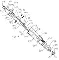
- FIG. 5 is a schematic partial cross sectional isometric view of a second exemplary embodiment of a Coaxial Impedance Matching Adapter, shown attached to a coaxial cable.
- FIG. 6 is a schematic partial cross sectional side view, the cross section normal to a plane of the printed circuit board, of the Coaxial Impedance Matching Adapter of FIG. 5 .
- FIG. 7 is a close-up view of area A of FIG. 6 .
- FIG. 8 is an exploded isometric view of the printed circuit board and ground block of FIG. 6 .
- FIG. 9 is an exploded isometric view of a first alternative printed circuit board and ground block configuration.
- FIG. 10 is an exploded isometric view of a second alternative printed circuit board and ground block configuration.
- FIG. 11 is a schematic cross sectional side view of a third exemplary embodiment of a Coaxial Impedance Matching Device.
- FIG. 12 is a network analyzer plot of a printed circuit board microstrip assembly from the Coaxial Impedance Matching Device of FIG. 5 , wherein measurements were taken with the printed circuit board separate from the enclosure.
- the inventor(s) have recognized that, due to the larger dimensions of 50 ohm characteristic impedance transmission lines and connectors, 50 ohm characteristic impedance systems have a significantly higher materials, manufacturing, logistics and installation cost than systems having higher characteristic impedances. Further, the inventors have recognized that a cost efficient inline coaxial impedance matching adapter with low insertion loss and signal degradation characteristics would enable use of, for example, 75 ohm characteristic impedance interconnecting transmission lines and connectors within an otherwise 50 ohm characteristic impedance system, thereby achieving a significant cost savings.
- FIGS. 1-4 A first exemplary embodiment of a Coaxial Impedance Matching Adapter (CIMA) 2 is demonstrated in FIGS. 1-4 .
- the CIMA 2 may be configured for in-line insertion between sections of coaxial transmission line and/or various RF devices such as radios and antennas.
- the CIMA 2 may be designed for insertion via standardized or proprietary coaxial connector interfaces or via direct interconnection with and/or between two coaxial cable transmission lines.
- the first exemplary embodiment demonstrates a CIMA 2 configuration for 50 ohm characteristic impedance transmission line at a first end 4 and for a standardized coaxial connector interface commonly used for 75 ohm characteristic impedance transmission lines/equipment at a second end 6 .
- the first end 4 and the second end 6 are also applied herein as identifiers for respective ends of discrete elements of the CIMA 2 , to identify same according to their alignment along a longitudinal axis of the CIMA 2 extending between the first end 4 and the second end 6 .
- a microstrip transmission line is contained within an environmentally sealed cavity 7 formed enclosed by a body portion 8 and a mating cap portion 10 .
- the microstrip transmission line is formed as a trace 12 on a first side 14 of a printed circuit board (PCB) 16 ( FIG. 2 ) having a ground plane 18 on a second side 20 ( FIG. 3 ).
- PCB printed circuit board
- the PCB 16 substrate material is preferably selected to be a microwave quality substrate having a high and uniform dielectric constant.
- the microstrip transmission line trace 12 may be derived from a series of Chebyshev 1 ⁇ 4 wavelength spaced apart trace 12 width step(s) 22 that reduce the trace 12 width from a wide width at the low impedance end, here the first end 4 , to a narrower width at the high impedance end, here the second end 6 .
- the number of steps(s) 22 each separated, for example, by 1 ⁇ 4 wavelength of a desired operating frequency of the CIMA 2 , is determined by the desired operating bandwidth, with more step(s) 22 increasing the bandwidth characteristics of the CIMA 2 .
- microstrip parameters may be applied to tune for specific portions of the desired frequency band with respect to specific step(s) 22 , bend(s) 24 and/or the placement of nearby ground field sources, such as the cavity sidewall(s) 13 and/or fastener(s) 29 .
- Alternative trace 12 solutions include 1 ⁇ 4 wave stub resonator filters aligned in parallel or series configurations, and/or various microstrip bandpass filters. Any trace solution which net transforms the characteristic impedance may be applied, including bandwith tuned microstrip traces.
- the inventors have recognized that, because the manufacture of an enclosing metal housing of extended length with a high tolerance bore and suitable strength characteristics may represent a significant portion of the resulting device cost, the overall length of the PCB 16 should be reduced.
- the trace 12 is formed with a bended and/or doubled back sinuous path including a series of sharp and/or arcuate bend(s) 24 that route the trace 1 2 away from and then back to a centerline of the longitudinal axis of the CIMA 2 , resulting in the trace 12 having a length greater than a longitudinal axis length of the PCB 16 .
- Each bend 24 may create an opportunity for signal degradation.
- the bend(s) 24 of the present embodiment are demonstrated with shallow angles, such as 45 degrees, and a miter corner is demonstrated applied to the outer side 26 of each bend 24 .
- the step(s) 22 may be located at linear portions of the trace 12 , such as midpoints of linear trace 12 segments between each of the bend(s) 24 .
- the body portion 8 and mating cap portion 10 that together form the surrounding enclosure are demonstrated as being formed with a coaxial bore that forms a cavity 7 for the PCB 16 with a first diameter 28 at either end and a larger second diameter 30 in a mid portion.
- the PCB 16 is dimensioned to seat within the cavity 7 , the PCB 16 dimensions matching a cross section of the cavity 7 , the trace 12 aligned with the longitudinal axis at the first end 4 and the second end 6 for interconnection with an inner conductor 31 of the respective coaxial transmission line 33 (see FIG. 5 ) and/or coaxial connector interfaces applied to each of the first and second ends 4 , 6 .
- connection to the inner conductor(s) 31 is via a first contact 42 surrounded adjacent the PCB 16 by a first end insulator 44 and a second contact 46 surrounded adjacent the PCB 16 by a second end insulator 48 .
- the first and second contact(s) 42 , 46 may be coupled to the trace 12 by soldering a preferably less than half diameter section of each thereto, thus maintaining axial alignment of the first side 14 of the PCB 16 , and thus the interconnections with the trace 12 , to the enclosure.
- the ground plane 18 applied to the second side 20 of the PCB 16 may be spaced slightly away from the PCB 16 periphery so that interconnection between the ground plane 18 and the enclosure sidewall(s) 13 is limited to ground contact(s) 32 placed proximate the first end 4 and second end 6 of the PCB 16 , respectively.
- the ground contact(s) 32 extend along the width of the PCB 16 on the second side 20 at each end and extend radially outward to the first diameter 28 .
- a plurality of spring finger(s) 34 oriented to extend toward a center of the cavity, provide a secure electromechanical contact with the enclosure sidewall(s) 13 .
- the CIMA 2 may be assembled by preparing a sub-assembly of the PCB 16 , ground contact(s) 32 , any supporting structure, the first and second contact(s) 42 , 46 and respective first and second end insulator(s) 44 , 48 . Insulator mating surfaces of the first and second contact(s) 42 , 46 may be knurled to rotationally interlock them with their respective insulator.
- the sub-assembly may then be inserted into the bore of the body portion 8 , the PCB 16 seating within the first diameter 28 and second diameter 30 , the second end 6 ground contact 32 spring finger(s) 34 engaging the first diameter 28 , and the second end insulator 48 passing through and seating within an inner conductor bore 50 , mating surfaces of which may also be knurled to prevent rotation of the respective first and second end insulator(s) 44 , 48 therein.
- a supporting structure such as a support block 36 may be applied to the second side 20 and/or within the body portion 8 .
- a fastener screw 41 passing through the sidewall 30 may be applied to secure the support block 36 against the second diameter sidewall 30 .
- the support block 36 is configured to receive a tension bar 38 that extends between contact with each of the ground contact(s) 32 proximate the first diameter 28 .
- a tension screw 40 also passing through the sidewall 30 and support block 36 , is positioned to retain and bias the tension bar 38 into secure supporting contact with the ground contacts 32 after the PCB 16 with attached ground contacts 32 is inserted into the cavity 7 of the body portion 8 .
- the sub-assembly may be axially locked within the body portion 8 by an outward projecting shoulder 49 formed in the second insulator 48 (see FIG. 6 ) and dielectric key(s) 52 that seat in a retaining groove 54 of the second end insulator 48 adjacent a second end 6 shoulder 58 of the inner conductor bore 50 .
- the dielectric key(s) 52 are then retained by a dielectric retainer 56 that fits between the dielectric key(s) 52 and the second end 6 bore sidewall, preventing radial movement of the dielectric key(s) 52 out of engagement with the retaining groove 54 .
- the PCB 16 is sealed within the cavity 7 by placing the cap portion 10 over the first end 4 of the body portion 8 .
- the first contact passes through a corresponding inner conductor bore 50 of the cap portion 10 and the first end insulator 44 is seated therein, the first end 4 of the PCB 16 seating within a first diameter 28 of the cap portion 10 , and the first end 4 ground contact 32 spring finger(s) 34 engaging the first diameter 28 .
- the cap portion 10 and the body portion 8 engage, for example, with overlapping annular shoulder portions that seat against each other.
- the cap portion 10 and the body portion 8 may be permanently joined together, sealing the PCB 16 there within, for example by a swage operation bending the outer overlapping annular shoulder portion over the inner overlapping shoulder.
- the body portion 8 and the cap portion 10 may be provided with a threaded interconnection.
- the first and second contacts 42 , 46 may each be provided with a spring basket 60 for receiving and securely gripping the inner conductor 31 of a mating connector or coaxial cable transmission line 33 .
- a compression member 62 may be provided on one or both of the connection interfaces to improve connection characteristics of the first and or second contact(s) 42 , 46 .
- the compression member 62 may be retained, for example, by a snap connection into an inner diameter annular compression member groove 64 proximate the respective end of the CIMA 2 along the extent of which the compression member 62 is axially movable.
- a wedge surface 66 formed on an inner diameter of an aperture of the compression member 62 is dimensioned to mate with a ramp surface 68 formed on distal ends of spring fingers extending from the dielectric retainer 56 over the spring fingers that together form the spring basket 60 .
- the wedge surface 66 engages the ramp surface 68 , biasing the ramp surface 68 radially inward and thereby the spring basket 60 radially inward to more securely grip the mating inner conductor 31 .
- the overall length of the PCB 16 is shortened as a function of the distance the bend(s) 24 allow the trace 12 to be spaced away from the longitudinal axis in a sinuous path, resulting in the trace 12 having a longer length than a longitudinal axis length of the PCB 16 .
- spacing the trace 12 away from the longitudinal axis also increases the required diameter of the surrounding enclosure.
- a second exemplary embodiment demonstrates an alternative trace 12 layout that includes a sinuous path in which bend(s) 24 are arranged to direct the trace 12 back upon itself and/or across the longitudinal axis to enable a reduction of the CIMA 2 overall length and/or second diameter 30 and thus the size of the surrounding enclosure, potentially with a trade-off with electrical performance.
- the bends are also demonstrated with a continuous width, i.e. inside and outside edges formed as arc segments with a common radius centerpoint.
- the trace 12 may be spaced away from the enclosure sidewall by, for example, a minimum of at least four times the trace 12 width from each edge.
- the PCB 16 is supported in the second exemplary embodiment by a ground block 70 that also provides a secure electrical interconnection between the ground plane 18 , the cap portion 10 and the body portion 8 .
- a ground block 70 that also provides a secure electrical interconnection between the ground plane 18 , the cap portion 10 and the body portion 8 .
- first and second ends 4 , 6 of the ground block 70 are demonstrated formed with a projecting rim 72 that mates with, for example, a ground groove 74 formed in each of the cap portion 10 second end 6 and the body portion 8 first end, each proximate and coaxial with the inner conductor bore 50 .
- the projecting rim 72 may have a flexure characteristic, the projecting rim 72 formed with a slight, for example outward, misalignment with the ground groove 74 , resulting in a bias between the ground groove(s) 74 and the respective projecting rim(s) 72 when assembled, thereby, providing a secure electrical interconnection therebetween.
- the ground block 70 may be coupled to the ground plane 18 on the second side 20 of the PCB 16 via a retainer 76 such as solder and/or conductive adhesive.
- the ground block 70 may be dimensioned with a narrowed midsection and/or coupled with the assistance of fastener(s) 29 or orientation posts of the ground block 70 projecting through corresponding apertures of the PCB 16 .
- the ground block 70 may be provided with a cavity to further reduce materials cost and/or weight.
- the projecting rim 72 may be formed with a flexure characteristic without overhanging edges along a mold break line, enabling cost effective manufacture by die casting, metal injection molding or the like.
- FIGS. 6 and 7 Further stabilization and/or support of the PCB 16 and ground block 70 may be provided by an annular protrusion 73 of the first end 4 of the second insulator 48 and the second end 6 of the first insulator 44 that keys with a corresponding annular groove 74 of the first and second ends 4 , 6 of the ground block 70 and/or the PCB 16 , as shown for example in FIGS. 6 and 7 .
- the insulator keylock arrangement may be simplified, for example as demonstrated in FIG. 11 , where both ends of the CIMA 2 are configured as coaxial connector interfaces.
- a plot of the PCB 16 of FIGS. 8-10 has been bench tested with a network analyzer separate from the enclosing metal housing, demonstrating viability of the trace 12 configuration for use over a target bandwidth of between at least 698 MHz and 3 Ghz.
- the CIMA 2 may similarly be configured with a multi-layer and/or multiple printed circuit board(s) 16 , for example in a strip line, rather than microstrip configuration.
- the CIMA 2 may provide an improvement in the signal characteristics, materials and manufacturing costs of an in-line impedance matching device to a level that enables previously impractical substitution of lower cost higher characteristic impedance transmission line and components into multi-band microwave communications systems.
- an in-line connector terminated coaxial body embodiment has been described in detail, one skilled in the art will appreciate that any manner of enclosure may also be applied, including incorporating the PCB 16 into enclosures, for example, formed in non-coaxial configurations such as rectangular cast metal or polymeric enclosures provided with connection interfaces on desired or common sides.
- the sub-assembly may be incorporated with further equipment and or circuits into existing enclosures with appropriate stand offs applied to isolate the PCB 16 from nearby electrical fields and or shorting surfaces.
Abstract
Description
| Table of |
| 2 | Coaxial |
| 4 | |
| 6 | |
| 7 | |
| 8 | |
| 10 | |
| 12 | |
| 13 | |
| 14 | |
| 16 | printed |
| 18 | |
| 20 | |
| 22 | |
| 24 | |
| 26 | |
| 28 | |
| 29 | |
| 30 | |
| 31 | |
| 32 | |
| 33 | coaxial |
| 34 | |
| 36 | |
| 38 | |
| 40 | |
| 41 | |
| 42 | |
| 44 | |
| 46 | |
| 48 | |
| 49 | outward projecting |
| 50 | inner conductor bore |
| 52 | dielectric key |
| 54 | retaining |
| 56 | |
| 58 | |
| 60 | |
| 62 | |
| 64 | |
| 66 | |
| 68 | |
| 70 | |
| 72 | projecting |
| 73 | |
| 74 | |
| 75 | |
| 76 | retainer |
Claims (21)
Priority Applications (3)
| Application Number | Priority Date | Filing Date | Title |
|---|---|---|---|
| US12/423,970 US7898357B2 (en) | 2008-05-12 | 2009-04-15 | Coaxial impedance matching adapter and method of manufacture |
| EP09006005A EP2120282A1 (en) | 2008-05-12 | 2009-04-30 | Coaxial impedance matching adapter and method of manufacture |
| JP2009115913A JP2009277656A (en) | 2008-05-12 | 2009-05-12 | Coaxial impedance matching adapter and method of manufacture |
Applications Claiming Priority (2)
| Application Number | Priority Date | Filing Date | Title |
|---|---|---|---|
| US5260608P | 2008-05-12 | 2008-05-12 | |
| US12/423,970 US7898357B2 (en) | 2008-05-12 | 2009-04-15 | Coaxial impedance matching adapter and method of manufacture |
Publications (2)
| Publication Number | Publication Date |
|---|---|
| US20090278622A1 US20090278622A1 (en) | 2009-11-12 |
| US7898357B2 true US7898357B2 (en) | 2011-03-01 |
Family
ID=40791287
Family Applications (1)
| Application Number | Title | Priority Date | Filing Date |
|---|---|---|---|
| US12/423,970 Expired - Fee Related US7898357B2 (en) | 2008-05-12 | 2009-04-15 | Coaxial impedance matching adapter and method of manufacture |
Country Status (3)
| Country | Link |
|---|---|
| US (1) | US7898357B2 (en) |
| EP (1) | EP2120282A1 (en) |
| JP (1) | JP2009277656A (en) |
Cited By (1)
| Publication number | Priority date | Publication date | Assignee | Title |
|---|---|---|---|---|
| US9009960B2 (en) | 2013-01-25 | 2015-04-21 | Commscope Technologies Llc | Method of manufacturing a curved transition surface of an inner contact |
Families Citing this family (3)
| Publication number | Priority date | Publication date | Assignee | Title |
|---|---|---|---|---|
| US9673604B2 (en) | 2015-05-05 | 2017-06-06 | Gregory L. Weipert | Coaxial cable terminator assembly having a substrate with inner and outer termination connections carried by a cap |
| CN110277704B (en) | 2018-03-14 | 2022-12-09 | 康普技术有限责任公司 | Coaxial offset T-shaped connector |
| WO2019217521A1 (en) * | 2018-05-08 | 2019-11-14 | Molex, Llc | Coaxial connector system |
Citations (26)
| Publication number | Priority date | Publication date | Assignee | Title |
|---|---|---|---|---|
| US2531437A (en) | 1942-03-31 | 1950-11-28 | Sperry Corp | Wave guide impedance transformer |
| US2533239A (en) | 1944-11-16 | 1950-12-12 | Int Standard Electric Corp | Impedance transformer for coaxial lines |
| US3209287A (en) | 1960-08-09 | 1965-09-28 | Bendix Corp | Electrical coaxial cable connecting assembly with impedance matching |
| US3440573A (en) * | 1964-08-19 | 1969-04-22 | Jesse L Butler | Electrical transmission line components |
| US4035748A (en) | 1974-09-26 | 1977-07-12 | Bunker Ramo Corporation | Coaxial impedance transducer pad |
| US4283694A (en) | 1978-07-11 | 1981-08-11 | U.S. Philips Corporation | Impedance-matching network realized in microstrip technique |
| US4610032A (en) | 1985-01-16 | 1986-09-02 | At&T Bell Laboratories | Sis mixer having thin film wrap around edge contact |
| US4951012A (en) | 1988-04-11 | 1990-08-21 | Siemens Aktiengesellschaft | Transformer arrangement to accomplish impedance transformation |
| US5233360A (en) | 1990-07-30 | 1993-08-03 | Sony Corporation | Matching device for a microstrip antenna |
| US5365203A (en) * | 1992-11-06 | 1994-11-15 | Susumu Co., Ltd. | Delay line device and method of manufacturing the same |
| JPH0955601A (en) | 1995-08-10 | 1997-02-25 | Mitsubishi Electric Corp | Microwave circuit device |
| US6323743B1 (en) | 1999-08-24 | 2001-11-27 | Tresness Irrevocable Patent Trust | Electronic filter assembly |
| US6411180B1 (en) | 1999-04-16 | 2002-06-25 | Telefonaktiebolaget Lm Ericsson (Publ) | Filter |
| US6636129B2 (en) | 2001-01-31 | 2003-10-21 | Eagle Comtronics, Inc. | Two-tiered tuned filter |
| US6639487B1 (en) | 1999-02-02 | 2003-10-28 | Nokia Corporation | Wideband impedance coupler |
| US6642819B1 (en) | 2001-11-30 | 2003-11-04 | Anokiwave, Inc. | Method and bend structure for reducing transmission line bend loss |
| US6791436B2 (en) | 1999-12-08 | 2004-09-14 | Eagle Comtronics, Inc. | Modular electrical signal filter assembly |
| US6794957B2 (en) | 2002-12-03 | 2004-09-21 | John Mezzalingua Associates, Inc. | CATV filter assembly with improved electrical grounding |
| US20050162238A1 (en) | 2004-01-23 | 2005-07-28 | Chung-Shun Ho | Structure of a wave filter |
| US7075385B2 (en) | 2004-04-29 | 2006-07-11 | Kathrein-Werke Kg | Impedance converter device |
| US7094104B1 (en) | 2005-05-04 | 2006-08-22 | Andrew Corporation | In-line coaxial circuit assembly |
| US7142073B2 (en) | 2004-06-29 | 2006-11-28 | Intel Corporation | Transmission line impedance matching |
| US7255599B1 (en) | 2006-08-31 | 2007-08-14 | John Mezzalingua Associates, Inc. | Impedance matched waterproof connector for CATV filter housing |
| US7278887B1 (en) | 2006-05-30 | 2007-10-09 | John Mezzalingua Associates, Inc. | Integrated filter connector |
| US7323951B2 (en) | 2005-07-13 | 2008-01-29 | John Mezzalinqua Associates, Inc. | Casing for CATV filter |
| US7348865B2 (en) | 2003-03-07 | 2008-03-25 | Ericsson Telecommunicacoes S.A. | Impedance-matching coupler |
Family Cites Families (3)
| Publication number | Priority date | Publication date | Assignee | Title |
|---|---|---|---|---|
| JP2001054083A (en) * | 1999-08-06 | 2001-02-23 | Nippon Antenna Co Ltd | Attenuator for cable modem |
| FR2804250B1 (en) * | 2000-01-24 | 2002-05-31 | Radiall Sa | COAXIAL ELECTRICAL CONNECTOR ELEMENT AND COAXIAL ELECTRICAL CONNECTOR COMPRISING SUCH AN ELEMENT |
| JP2003069311A (en) * | 2001-08-24 | 2003-03-07 | Japan Radio Co Ltd | Meander line |
-
2009
- 2009-04-15 US US12/423,970 patent/US7898357B2/en not_active Expired - Fee Related
- 2009-04-30 EP EP09006005A patent/EP2120282A1/en not_active Withdrawn
- 2009-05-12 JP JP2009115913A patent/JP2009277656A/en active Pending
Patent Citations (26)
| Publication number | Priority date | Publication date | Assignee | Title |
|---|---|---|---|---|
| US2531437A (en) | 1942-03-31 | 1950-11-28 | Sperry Corp | Wave guide impedance transformer |
| US2533239A (en) | 1944-11-16 | 1950-12-12 | Int Standard Electric Corp | Impedance transformer for coaxial lines |
| US3209287A (en) | 1960-08-09 | 1965-09-28 | Bendix Corp | Electrical coaxial cable connecting assembly with impedance matching |
| US3440573A (en) * | 1964-08-19 | 1969-04-22 | Jesse L Butler | Electrical transmission line components |
| US4035748A (en) | 1974-09-26 | 1977-07-12 | Bunker Ramo Corporation | Coaxial impedance transducer pad |
| US4283694A (en) | 1978-07-11 | 1981-08-11 | U.S. Philips Corporation | Impedance-matching network realized in microstrip technique |
| US4610032A (en) | 1985-01-16 | 1986-09-02 | At&T Bell Laboratories | Sis mixer having thin film wrap around edge contact |
| US4951012A (en) | 1988-04-11 | 1990-08-21 | Siemens Aktiengesellschaft | Transformer arrangement to accomplish impedance transformation |
| US5233360A (en) | 1990-07-30 | 1993-08-03 | Sony Corporation | Matching device for a microstrip antenna |
| US5365203A (en) * | 1992-11-06 | 1994-11-15 | Susumu Co., Ltd. | Delay line device and method of manufacturing the same |
| JPH0955601A (en) | 1995-08-10 | 1997-02-25 | Mitsubishi Electric Corp | Microwave circuit device |
| US6639487B1 (en) | 1999-02-02 | 2003-10-28 | Nokia Corporation | Wideband impedance coupler |
| US6411180B1 (en) | 1999-04-16 | 2002-06-25 | Telefonaktiebolaget Lm Ericsson (Publ) | Filter |
| US6323743B1 (en) | 1999-08-24 | 2001-11-27 | Tresness Irrevocable Patent Trust | Electronic filter assembly |
| US6791436B2 (en) | 1999-12-08 | 2004-09-14 | Eagle Comtronics, Inc. | Modular electrical signal filter assembly |
| US6636129B2 (en) | 2001-01-31 | 2003-10-21 | Eagle Comtronics, Inc. | Two-tiered tuned filter |
| US6642819B1 (en) | 2001-11-30 | 2003-11-04 | Anokiwave, Inc. | Method and bend structure for reducing transmission line bend loss |
| US6794957B2 (en) | 2002-12-03 | 2004-09-21 | John Mezzalingua Associates, Inc. | CATV filter assembly with improved electrical grounding |
| US7348865B2 (en) | 2003-03-07 | 2008-03-25 | Ericsson Telecommunicacoes S.A. | Impedance-matching coupler |
| US20050162238A1 (en) | 2004-01-23 | 2005-07-28 | Chung-Shun Ho | Structure of a wave filter |
| US7075385B2 (en) | 2004-04-29 | 2006-07-11 | Kathrein-Werke Kg | Impedance converter device |
| US7142073B2 (en) | 2004-06-29 | 2006-11-28 | Intel Corporation | Transmission line impedance matching |
| US7094104B1 (en) | 2005-05-04 | 2006-08-22 | Andrew Corporation | In-line coaxial circuit assembly |
| US7323951B2 (en) | 2005-07-13 | 2008-01-29 | John Mezzalinqua Associates, Inc. | Casing for CATV filter |
| US7278887B1 (en) | 2006-05-30 | 2007-10-09 | John Mezzalingua Associates, Inc. | Integrated filter connector |
| US7255599B1 (en) | 2006-08-31 | 2007-08-14 | John Mezzalingua Associates, Inc. | Impedance matched waterproof connector for CATV filter housing |
Non-Patent Citations (1)
| Title |
|---|
| European Search Report of counterpart EPO Application No. 09006005.4-1248, issued Aug. 7, 2009. |
Cited By (2)
| Publication number | Priority date | Publication date | Assignee | Title |
|---|---|---|---|---|
| US9009960B2 (en) | 2013-01-25 | 2015-04-21 | Commscope Technologies Llc | Method of manufacturing a curved transition surface of an inner contact |
| US9419351B2 (en) | 2013-01-25 | 2016-08-16 | Commscope Technologies Llc | Curved transition surface inner contact |
Also Published As
| Publication number | Publication date |
|---|---|
| US20090278622A1 (en) | 2009-11-12 |
| JP2009277656A (en) | 2009-11-26 |
| EP2120282A1 (en) | 2009-11-18 |
Similar Documents
| Publication | Publication Date | Title |
|---|---|---|
| US11024931B2 (en) | In-line filter having mutually compensating inductive and capacitive coupling | |
| US8089327B2 (en) | Waveguide to plural microstrip transition | |
| US8384492B2 (en) | Coaxial line to microstrip connector having slots in the microstrip line for receiving an encircling metallic plate | |
| US9647306B2 (en) | RF filter comprising N coaxial resonators arranged in a specified interdigitation pattern | |
| KR102206702B1 (en) | Cavity Filter | |
| US8152534B1 (en) | Connector used for connecting a coaxial cable and a microstrip | |
| US20080278259A1 (en) | Methods for designing switchable and tunable broadband filters using finite-width conductor-backed coplanar waveguide structures | |
| US7898357B2 (en) | Coaxial impedance matching adapter and method of manufacture | |
| US8797125B2 (en) | Filter arrangement | |
| Nouri et al. | Compact 5G millimeter‐wave dual‐band filter with application in filtenna | |
| CN107004937B (en) | Radio frequency connecting device | |
| US7095300B2 (en) | Band eliminate filter and communication apparatus | |
| CN101582530A (en) | Coaxial impedance matching adapter and method of manufacture | |
| RU2487465C1 (en) | Microwave power amplifier | |
| EP2387096B1 (en) | Transmission line impedance transformer and related methods | |
| US9627740B2 (en) | RF notch filters and related methods | |
| CN103299482A (en) | Microstrip to airstrip transition with low passive inter-modulation | |
| CN109301406B (en) | Bandwidth-adjustable miniaturized filtering integrated three-dimensional balun | |
| US20150061950A1 (en) | Small digital tunable antenna systems for wireless applications | |
| WO2019217521A1 (en) | Coaxial connector system | |
| JP2007295361A (en) | Duplexer | |
| US11916276B2 (en) | Circulator conductor and housing configuration | |
| Patel et al. | Wilkinson type lumped element combiner-splitter for indigenous amplifier development | |
| KR102437893B1 (en) | Irreversible element with resonant circuit | |
| KR102307551B1 (en) | Irreversible element with resonant circuit |
Legal Events
| Date | Code | Title | Description |
|---|---|---|---|
| AS | Assignment |
Owner name: ANDREW LLC, NORTH CAROLINA Free format text: ASSIGNMENT OF ASSIGNORS INTEREST;ASSIGNORS:PHUYAL, PRATIBHA CHAULAGAI;VAN SWEARINGEN, KENDRICK;COX, ALBERT;AND OTHERS;REEL/FRAME:022548/0551 Effective date: 20090413 |
|
| AS | Assignment |
Owner name: BANK OF AMERICA, N.A., AS ADMINISTRATIVE AGENT,CAL Free format text: SECURITY AGREEMENT;ASSIGNORS:COMMSCOPE OF NORTH CAROLINA;ANDREW LLC;REEL/FRAME:023021/0481 Effective date: 20090728 Owner name: BANK OF AMERICA, N.A., AS ADMINISTRATIVE AGENT, CA Free format text: SECURITY AGREEMENT;ASSIGNORS:COMMSCOPE OF NORTH CAROLINA;ANDREW LLC;REEL/FRAME:023021/0481 Effective date: 20090728 |
|
| AS | Assignment |
Owner name: COMMSCOPE, INC. OF NORTH CAROLINA, NORTH CAROLINA Free format text: PATENT RELEASE;ASSIGNOR:BANK OF AMERICA, N.A., AS ADMINISTRATIVE AGENT;REEL/FRAME:026039/0005 Effective date: 20110114 Owner name: ANDREW LLC (F/K/A ANDREW CORPORATION), NORTH CAROL Free format text: PATENT RELEASE;ASSIGNOR:BANK OF AMERICA, N.A., AS ADMINISTRATIVE AGENT;REEL/FRAME:026039/0005 Effective date: 20110114 Owner name: ALLEN TELECOM LLC, NORTH CAROLINA Free format text: PATENT RELEASE;ASSIGNOR:BANK OF AMERICA, N.A., AS ADMINISTRATIVE AGENT;REEL/FRAME:026039/0005 Effective date: 20110114 |
|
| STCF | Information on status: patent grant |
Free format text: PATENTED CASE |
|
| AS | Assignment |
Owner name: JPMORGAN CHASE BANK, N.A., AS COLLATERAL AGENT, NE Free format text: SECURITY AGREEMENT;ASSIGNORS:ALLEN TELECOM LLC, A DELAWARE LLC;ANDREW LLC, A DELAWARE LLC;COMMSCOPE, INC. OF NORTH CAROLINA, A NORTH CAROLINA CORPORATION;REEL/FRAME:026276/0363 Effective date: 20110114 |
|
| AS | Assignment |
Owner name: JPMORGAN CHASE BANK, N.A., AS COLLATERAL AGENT, NE Free format text: SECURITY AGREEMENT;ASSIGNORS:ALLEN TELECOM LLC, A DELAWARE LLC;ANDREW LLC, A DELAWARE LLC;COMMSCOPE, INC OF NORTH CAROLINA, A NORTH CAROLINA CORPORATION;REEL/FRAME:026272/0543 Effective date: 20110114 |
|
| FPAY | Fee payment |
Year of fee payment: 4 |
|
| AS | Assignment |
Owner name: COMMSCOPE TECHNOLOGIES LLC, NORTH CAROLINA Free format text: CHANGE OF NAME;ASSIGNOR:ANDREW LLC;REEL/FRAME:035286/0001 Effective date: 20150301 |
|
| AS | Assignment |
Owner name: WILMINGTON TRUST, NATIONAL ASSOCIATION, AS COLLATERAL AGENT, CONNECTICUT Free format text: SECURITY INTEREST;ASSIGNORS:ALLEN TELECOM LLC;COMMSCOPE TECHNOLOGIES LLC;COMMSCOPE, INC. OF NORTH CAROLINA;AND OTHERS;REEL/FRAME:036201/0283 Effective date: 20150611 Owner name: WILMINGTON TRUST, NATIONAL ASSOCIATION, AS COLLATE Free format text: SECURITY INTEREST;ASSIGNORS:ALLEN TELECOM LLC;COMMSCOPE TECHNOLOGIES LLC;COMMSCOPE, INC. OF NORTH CAROLINA;AND OTHERS;REEL/FRAME:036201/0283 Effective date: 20150611 |
|
| AS | Assignment |
Owner name: REDWOOD SYSTEMS, INC., NORTH CAROLINA Free format text: RELEASE OF SECURITY INTEREST PATENTS (RELEASES RF 036201/0283);ASSIGNOR:WILMINGTON TRUST, NATIONAL ASSOCIATION;REEL/FRAME:042126/0434 Effective date: 20170317 Owner name: COMMSCOPE TECHNOLOGIES LLC, NORTH CAROLINA Free format text: RELEASE OF SECURITY INTEREST PATENTS (RELEASES RF 036201/0283);ASSIGNOR:WILMINGTON TRUST, NATIONAL ASSOCIATION;REEL/FRAME:042126/0434 Effective date: 20170317 Owner name: ALLEN TELECOM LLC, NORTH CAROLINA Free format text: RELEASE OF SECURITY INTEREST PATENTS (RELEASES RF 036201/0283);ASSIGNOR:WILMINGTON TRUST, NATIONAL ASSOCIATION;REEL/FRAME:042126/0434 Effective date: 20170317 Owner name: COMMSCOPE, INC. OF NORTH CAROLINA, NORTH CAROLINA Free format text: RELEASE OF SECURITY INTEREST PATENTS (RELEASES RF 036201/0283);ASSIGNOR:WILMINGTON TRUST, NATIONAL ASSOCIATION;REEL/FRAME:042126/0434 Effective date: 20170317 |
|
| FEPP | Fee payment procedure |
Free format text: MAINTENANCE FEE REMINDER MAILED (ORIGINAL EVENT CODE: REM.); ENTITY STATUS OF PATENT OWNER: LARGE ENTITY |
|
| LAPS | Lapse for failure to pay maintenance fees |
Free format text: PATENT EXPIRED FOR FAILURE TO PAY MAINTENANCE FEES (ORIGINAL EVENT CODE: EXP.); ENTITY STATUS OF PATENT OWNER: LARGE ENTITY |
|
| STCH | Information on status: patent discontinuation |
Free format text: PATENT EXPIRED DUE TO NONPAYMENT OF MAINTENANCE FEES UNDER 37 CFR 1.362 |
|
| AS | Assignment |
Owner name: ALLEN TELECOM LLC, ILLINOIS Free format text: RELEASE BY SECURED PARTY;ASSIGNOR:JPMORGAN CHASE BANK, N.A.;REEL/FRAME:048840/0001 Effective date: 20190404 Owner name: COMMSCOPE, INC. OF NORTH CAROLINA, NORTH CAROLINA Free format text: RELEASE BY SECURED PARTY;ASSIGNOR:JPMORGAN CHASE BANK, N.A.;REEL/FRAME:048840/0001 Effective date: 20190404 Owner name: ANDREW LLC, NORTH CAROLINA Free format text: RELEASE BY SECURED PARTY;ASSIGNOR:JPMORGAN CHASE BANK, N.A.;REEL/FRAME:048840/0001 Effective date: 20190404 Owner name: COMMSCOPE TECHNOLOGIES LLC, NORTH CAROLINA Free format text: RELEASE BY SECURED PARTY;ASSIGNOR:JPMORGAN CHASE BANK, N.A.;REEL/FRAME:048840/0001 Effective date: 20190404 Owner name: REDWOOD SYSTEMS, INC., NORTH CAROLINA Free format text: RELEASE BY SECURED PARTY;ASSIGNOR:JPMORGAN CHASE BANK, N.A.;REEL/FRAME:048840/0001 Effective date: 20190404 Owner name: ANDREW LLC, NORTH CAROLINA Free format text: RELEASE BY SECURED PARTY;ASSIGNOR:JPMORGAN CHASE BANK, N.A.;REEL/FRAME:049260/0001 Effective date: 20190404 Owner name: REDWOOD SYSTEMS, INC., NORTH CAROLINA Free format text: RELEASE BY SECURED PARTY;ASSIGNOR:JPMORGAN CHASE BANK, N.A.;REEL/FRAME:049260/0001 Effective date: 20190404 Owner name: COMMSCOPE TECHNOLOGIES LLC, NORTH CAROLINA Free format text: RELEASE BY SECURED PARTY;ASSIGNOR:JPMORGAN CHASE BANK, N.A.;REEL/FRAME:049260/0001 Effective date: 20190404 Owner name: COMMSCOPE, INC. OF NORTH CAROLINA, NORTH CAROLINA Free format text: RELEASE BY SECURED PARTY;ASSIGNOR:JPMORGAN CHASE BANK, N.A.;REEL/FRAME:049260/0001 Effective date: 20190404 Owner name: ALLEN TELECOM LLC, ILLINOIS Free format text: RELEASE BY SECURED PARTY;ASSIGNOR:JPMORGAN CHASE BANK, N.A.;REEL/FRAME:049260/0001 Effective date: 20190404 |
|
| FP | Lapsed due to failure to pay maintenance fee |
Effective date: 20190301 |
|
| AS | Assignment |
Owner name: JPMORGAN CHASE BANK, N.A., NEW YORK Free format text: TERM LOAN SECURITY AGREEMENT;ASSIGNORS:COMMSCOPE, INC. OF NORTH CAROLINA;COMMSCOPE TECHNOLOGIES LLC;ARRIS ENTERPRISES LLC;AND OTHERS;REEL/FRAME:049905/0504 Effective date: 20190404 Owner name: WILMINGTON TRUST, NATIONAL ASSOCIATION, AS COLLATE Free format text: PATENT SECURITY AGREEMENT;ASSIGNOR:COMMSCOPE TECHNOLOGIES LLC;REEL/FRAME:049892/0051 Effective date: 20190404 Owner name: JPMORGAN CHASE BANK, N.A., NEW YORK Free format text: ABL SECURITY AGREEMENT;ASSIGNORS:COMMSCOPE, INC. OF NORTH CAROLINA;COMMSCOPE TECHNOLOGIES LLC;ARRIS ENTERPRISES LLC;AND OTHERS;REEL/FRAME:049892/0396 Effective date: 20190404 Owner name: WILMINGTON TRUST, NATIONAL ASSOCIATION, AS COLLATERAL AGENT, CONNECTICUT Free format text: PATENT SECURITY AGREEMENT;ASSIGNOR:COMMSCOPE TECHNOLOGIES LLC;REEL/FRAME:049892/0051 Effective date: 20190404 |