US7908424B2 - Memory card and data rewriting method - Google Patents
Memory card and data rewriting method Download PDFInfo
- Publication number
- US7908424B2 US7908424B2 US11/802,998 US80299807A US7908424B2 US 7908424 B2 US7908424 B2 US 7908424B2 US 80299807 A US80299807 A US 80299807A US 7908424 B2 US7908424 B2 US 7908424B2
- Authority
- US
- United States
- Prior art keywords
- command
- data
- enable register
- value
- invalidity
- Prior art date
- Legal status (The legal status is an assumption and is not a legal conclusion. Google has not performed a legal analysis and makes no representation as to the accuracy of the status listed.)
- Expired - Fee Related, expires
Links
Images


Classifications
-
- G—PHYSICS
- G06—COMPUTING; CALCULATING OR COUNTING
- G06K—GRAPHICAL DATA READING; PRESENTATION OF DATA; RECORD CARRIERS; HANDLING RECORD CARRIERS
- G06K19/00—Record carriers for use with machines and with at least a part designed to carry digital markings
- G06K19/06—Record carriers for use with machines and with at least a part designed to carry digital markings characterised by the kind of the digital marking, e.g. shape, nature, code
- G06K19/067—Record carriers with conductive marks, printed circuits or semiconductor circuit elements, e.g. credit or identity cards also with resonating or responding marks without active components
- G06K19/07—Record carriers with conductive marks, printed circuits or semiconductor circuit elements, e.g. credit or identity cards also with resonating or responding marks without active components with integrated circuit chips
-
- G—PHYSICS
- G06—COMPUTING; CALCULATING OR COUNTING
- G06F—ELECTRIC DIGITAL DATA PROCESSING
- G06F13/00—Interconnection of, or transfer of information or other signals between, memories, input/output devices or central processing units
- G06F13/14—Handling requests for interconnection or transfer
- G06F13/16—Handling requests for interconnection or transfer for access to memory bus
- G06F13/1668—Details of memory controller
Definitions
- the present invention relates to a memory card, and more particularly to a technique that can be effectively applied to flexible adaptation to changes in or additions to standards of a multimedia card.
- Multimedia cards are extensively known as one type of external storage media for use in personal computers, multifunctional terminal unit and the like.
- a multimedia card can be used for recording any kind of digital information such as in recording still pictures in a digital video camera, recording data in a mobile telephone or in recording music in a portable phonogram player.
- MMCA Multimedia Card Association
- a multimedia card is a young product item having come into being along with the expanding use of the Internet and of mobile telephones, and there are frequent revisions in or additions to the multimedia card standards.
- An object of the present invention is to provide a memory card and a data rewriting method therefore making possible adaptation to any revision in or addition to the standards at low cost and in a short period of time by merely altering the firmware.
- a memory card has a controller, and the controller comprises: a command decoding unit for decoding externally issued commands; an index setting unit in which the validity or invalidity is set for the index of each of said externally issued commands; and a command detection signal generating unit for judging whether each of the externally issued commands is valid or invalid on the basis of the result of decoding by the command decoding unit and a value set by the index setting unit, and supplying the result as a detection signal.
- the index setting unit is a register, and the setting of the validity or invalidity of each command can be altered as desired on the basis of firmware data.
- the controller comprises: a command decoding unit for decoding externally issued commands, judging the index of each of the commands, and supplying a decoded signal to a prescribed destination; an index setting unit in which the validity or invalidity of each of the commands is set for each index; and a command detection signal generating unit for identifying from the decoded signal from the command decoding unit the index of the externally issued command, judging the validity or invalidity of the command of the identified index from data set in the index setting unit and, if the command is valid, executing response processing matching the command and supplying a detection signal to have processing prescribed by the command executed.
- the controller comprises: a data detecting unit for detecting externally entered data forms; a data form setting unit in which data indicating the validity or invalidity of the externally entered data form is set for each data form; and a data detection signal generating unit for judging the validity or invalidity of the externally issued data on the basis of the result of detection by the data detecting unit and a value set by the data form setting unit, and supplying the result as a detection signal.
- the data form setting unit is a register, and the setting of the validity or invalidity of each data form can be altered as desired on the basis of firmware data.
- a data writing method for memory cards comprising the steps of:
- a data writing method for memory cards comprising the steps of:
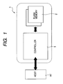
- FIG. 1 is a block diagram of a memory card in one mode for carrying out the present invention
- FIG. 2 is a block diagram of a controller provided in the memory card of FIG. 1 ;
- FIG. 3 illustrates the operation of the controller when it has received a command set to be valid in a command enable register provided in the memory card of FIG. 1 ;
- FIG. 4 illustrates the operation of the controller when it has received a command set to be invalid in a command enable register provided in the memory card of FIG. 1 ;
- FIG. 5 is a flow chart showing the write sequence of firmware to alter the setting in the memory card of FIG. 1 ;
- FIG. 6 is a flow chart of the sequence of operations to alter the setting of register data in the command enable register in the memory card of FIG. 1 ;
- FIG. 7 illustrates the configuration of data serially transferred to the memory card of FIG. 1 ;
- FIG. 8 illustrates examples of start byte in the data of FIG. 7 ;
- FIG. 9 illustrates the operation of the controller provided in a memory card in another mode for carrying out the invention.
- FIG. 10 illustrates examples of register data set in the command enable register of the memory card in the other mode for carrying out the invention.
- a memory card 1 consists of a multimedia card, and used as an external storage medium of a host HT in a digital video camera, mobile telephone, portable phonogram player or personal computer.
- the memory card 1 as shown in FIG. 1 , consists of a flash memory (nonvolatile semiconductor memory) 2 and a controller 3 .
- the flash memory 2 is a nonvolatile semiconductor memory permit electrical rewriting and erasion of data.
- the controller 3 connected to the host HT, takes charge of control of the flash memory 2 , reads out programs and data stored in the flash memory 2 to subject them to prescribed processing, and instructs writing of data.
- the controller 3 comprises a control unit 4 , memories 5 and 5 a , a command decoding circuit (command decoding unit) 6 , a command detection signal generating circuit (command detection signal generating unit, a register) 7 , a command enable register (index setting unit) 8 , a data detecting circuit (data detecting unit) 9 , a data detection signal generating circuit (data detection signal generating unit) 10 , a data enable register (data form setting unit) 11 , and a control logic 12 .
- the control unit 4 judges whether given command and data form are valid or invalid on the basis of detection signal supplied from a command detection signal generating circuit 7 and a data detection signal generating circuit 10 . If they are found valid, it executes predetermined response processing and processing prescribed for each command, at the same time supplies an interrupt signal to the control logic 12 to inform it of the reception of the command, and processes a data transfer and other operations under the control of the control logic 12 .
- the memory 5 is a nonvolatile memory such as a read only memory (ROM) or an electrically erasable and programmable ROM (EEPROM), and the memory 5 a is a volatile memory such as a static random access memory (SRAM).
- ROM read only memory
- EEPROM electrically erasable and programmable ROM
- SRAM static random access memory
- the memory 5 is stored a control program for operating the control logic 12 and the like, and the memory 5 a is used as a work area for the control logic 12 .
- the command decoding circuit 6 decodes commands CMD 0 through CMDn transmitted from the host HT, and supplies the results of decoding to the command detection signal generating circuit 7 .
- These commands CMD 0 through CMDn issued by the host HT cover all the manners of processing instructed to the memory card 1 including recognition of the card, read, write and erase.
- the command detection signal generating circuit 7 consists of AND circuits 7 1 through 7 n , and these AND circuits 7 1 through 7 n are provided to respectively match the commands CMD 0 through CMDn.
- the command decoding circuit 6 supplies the results of decoding by any of the commands CMD 0 through CMDn to the matching one of the AND circuits 7 1 through 7 n .
- each of the AND circuits 7 1 through 7 n is connected to one input section of each of the AND circuits 7 1 through 7 n .
- the command decoding circuit 6 supplies its output, on the basis the results of decoding of any of the commands CMD 0 through CMDn, to the matching one of the AND circuits 7 1 through 7 n .
- each of the AND circuits 7 1 through 7 n is so connected that register data set in the command enable register 8 be entered.
- the command detection signal generating circuit 7 computes with the AND circuits 7 1 through 7 n the logical products of decoded signals from the command decoding circuit 6 and the register data set in the command enable register 8 , and supplies the control unit 4 with the detection signal of the pertinent command.
- the command enable register 8 stores and sets in advance as register data for each individual command index whether a command issued by the host HT is valid or invalid. In this case, a Hi signal is set for every valid command.
- the data detecting circuit 9 detects a data form issued by the host HT by a serial transfer, and supplies it to the data detection signal generating circuit 10 .
- the data detection signal generating circuit 10 consists of n AND circuits 10 1 through 10 n .
- each of the AND circuits 10 1 through 10 n To one input section of each of the AND circuits 10 1 through 10 n is connected the data detecting circuit 9 , and the data detecting circuit 9 supplies a signal of detection result to the matching one of the AND circuits 10 1 through 10 n .
- each of the AND circuits 10 1 through 10 n is so connected that register data set in the data enable register 11 be entered.
- the data detection signal generating circuit 10 computes with the AND circuits 10 1 through 10 n the logical products of decoded signals from the data detecting circuit 9 and the register data set in the data enable register 11 , and supplies the control unit 4 with a detection signal in the pertinent data form.
- the data enable register 11 which can set register data matching data forms No. 0 through No. n, it is set in advance as register data for each individual data form whether a data form received from the host HT is valid or invalid.
- a Hi signal is set for every valid command.
- the control logic 12 taking charge of control to set register data in the command enable register 8 and the data enable register 11 , also takes charge of every control in the controller 3 .
- FIG. 3 is a diagram illustrating the operation at the time a command is entered, the data detecting circuit 9 , the data detection signal generating circuit 10 and the data enable register 11 are omitted.
- this command CMD 1 is entered into the command decoding circuit 6 .
- the command decoding circuit 6 decodes the received command CMD 1 , and supplies the signal (Hi) of the result of decoding to one input section of the AND circuit 7 2 of the command detection signal generating circuit 7 matching the command CMD 1 .
- a Hi signal is entered into each of the two input sections of the AND circuit 7 2 , and from the AND circuits 7 2 is supplied a signal of the Hi level as the detection signal. Since no Hi signal is entered into any of the other AND circuits 7 1 through 7 n-1 , they supply Lo signals.
- control unit 4 When the control unit 4 receives the detection signal of the AND circuit 7 2 , the control unit 4 supplies an interrupt signal to the control logic 12 and, having received the interrupt signal, the control logic 12 executes response processing matching the command CMD 1 and processing prescribed by the command CMD 1 .
- FIG. 4 again, as it is a diagram illustrating the operation at the time a command is entered, the data detecting circuit 9 , the data detection signal generating circuit 10 and the data enable register 11 are omitted.
- the command CMDn is entered into the command decoding circuit 6 .
- the command decoding circuit 6 decodes the received command CMDn, and supplies a Hi signal to one input section of the AND circuit 7 n of the command detection signal generating circuit 7 matching the command CMDn.
- a Hi signal is entered into only one input section of the AND circuit 7 n , and no detection signal is supplied from the AND circuit 7 2 , with a Lo signal continuing to be supplied. Similarly in any of the other AND circuits 7 1 and 7 3 through 7 n , a Lo signal continues to be supplied as no Hi signal is entered into one of the input sections.
- control logic 12 ignores the entered command CMDn, and eventually the command CMDn is invalidated.
- step S 101 the memory card 1 before shipment as a product is mounted on an emulator, and a source voltage is fed to it. This causes the memory card 1 to undergo power-on resetting as initialization (step S 101 ).
- initial register data are set in the command enable register 8 .
- the memory card 1 Upon completion of the power-on resetting, the memory card 1 enters into a state of standing by for a command (step S 102 ).
- a debug command for use in rewriting or fault analysis of system information in the memory card is issued from the emulator (step S 103 ), and the memory card is shifted to a debug mode.
- firmware data including the altered register data are supplied on a module-by-module basis.
- step S 105 Upon reception by the memory card 1 of firmware data including the altered register data (step S 105 ), the control logic 12 writes the received firmware data into a specific area in the flash memory 2 (step S 106 ), and the writing of firmware data is thereby completed.
- control logic 12 When power supply to the memory card 1 is turned on, the control logic 12 is initialized (step S 201 ). After that, on the basis of firmware data stored in each memory, register data in the command enable register 8 are initialized (step S 202 ).
- control logic 12 searches a specific area in the flash memory 2 to check the presence or absence of any firmware (step S 203 ). If any firmware is found in the searched specific area in this processing at step S 203 , that firmware is read in and temporarily stored into the memory 5 a (step S 204 ).
- the control logic 12 newly sets register data of the command enable register 8 on the basis of the firmware data stored into the memory 5 a (step S 205 ), and completes the power-on resetting (step S 206 ).
- step S 206 Even if no firmware is found in the specific area in the processing of step S 203 , processing at step S 206 is also performed.
- the serial data to be transferred consist, as shown in FIG. 7 , of a start byte, data of 8 to 2048 bits and cycle redundancy codes (CRC) data of 16 bits.
- CRC cycle redundancy codes
- the start byte is a datum indicating the start of a data transfer.
- This start byte as shown in FIG. 8 , is separately set for the data form for single-block writing which allows the transfer of one block per command and that for multi-block writing which allows the transfer of a plurality of blocks per command.
- the data detecting circuit 9 will supply the signal (Hi) of the result of decoding to one of the input sections of the AND circuit 10 2 of the data detection signal generating circuit 10 matching the data form No. 1.
- the AND circuit 10 2 supplies a detection signal (Hi) indicating the detection of the data form No. 1.
- the control logic 12 Upon reception of the detection signal by the control unit 4 , the control logic 12 receives data transferred from the host HT and subjects them to prescribed processing.
- the AND circuit 10 2 of the data detection signal generating circuit 10 will supply a Lo signal, and therefore the control logic 12 will not accept data transferred from the host HT.
- the setting of the register data in this data enable register 11 can be altered by the above-described processing at steps S 101 through S 106 and steps S 201 through S 207 .
- the memory card 1 can be introduced to the market at low cost and in a short period of time.
- the memory card 1 in the above-described mode for carrying out the invention permits setting of the validity or invalidity of each of commands and data forms
- the memory card 1 can as well be provided with not only a function to set the validity or invalidity of these commands and data forms but also a function to select a response in the format prescribed for each command to be returned to the host HT.
- a controller 3 a of the memory card 1 has a configuration involving the addition of a response generating circuit 13 . Furthermore, a command enable register 8 a is additionally provided with a function to set a response type selection signal for selection the type of response matching each command index.
- the illustration of the data detecting circuit 9 , the data detection signal generating circuit 10 and the data enable register 11 is omitted.
- the response generating circuit 13 generates a response matching each of the command indexes on the basis of a response type selection signal set in the command enable register 8 a , and returns it to the host HT.
- the response generating circuit 13 generates from a response type selection signal of, for instance two bits, a matching response, and returns it to the host HT. It is supposed here that there are available alternatives of responses Type 0 through Type 3 , for instance, for the response to be returned to the host HT, and ‘00’ is set for the response Type 0 , ‘01’ for the Type 1 , ‘10’ for the response Type 2 and ‘11” for the response Type 3 .
- the response generating circuit 13 reads out a response type selection signal matching the command CMD 1 under the control of the control logic 12 .
- the response generating circuit 13 having read out the response signal ‘11’ generates a response of Type 3 matching the command CMD 1 , and returns it to the host HT.
- a register for restraining the occurrence of interrupt signals to the control logic 12 can be added to enable their occurrence in respect of each command.
- register data are to be set for each individual command, validity or invalidity can as well be set for each class of commands, such as basic commands, erase commands, read command and write commands.
- register data of validity (Hi) or invalidity (Lo) are separately set for the commands CMD 0 through CMD 6 as shown in the upper half of FIG. 10
- register data of validity or invalidity may as well be set collectively for commands CMD 0 through CMD 2 , command sCMD 3 and CMD 4 , and commands CMD 5 and CMD 6 as shown in the lower half of FIG. 10 .
- the memory card and data rewriting method according to the present invention is suitable for use in simplified techniques to adapt memory cards to any change in or addition to the applicable standards.
Abstract
Description
Claims (5)
Priority Applications (1)
| Application Number | Priority Date | Filing Date | Title |
|---|---|---|---|
| US11/802,998 US7908424B2 (en) | 2001-09-13 | 2007-05-29 | Memory card and data rewriting method |
Applications Claiming Priority (5)
| Application Number | Priority Date | Filing Date | Title |
|---|---|---|---|
| JP2001-278585 | 2001-09-13 | ||
| JP2001278585A JP4294894B2 (en) | 2001-09-13 | 2001-09-13 | Memory card |
| US10/486,651 US20040236909A1 (en) | 2001-09-13 | 2002-05-10 | Memory card and data rewriting method |
| PCT/JP2002/004548 WO2003025849A1 (en) | 2001-09-13 | 2002-05-10 | Memory card and data rewriting method |
| US11/802,998 US7908424B2 (en) | 2001-09-13 | 2007-05-29 | Memory card and data rewriting method |
Related Parent Applications (3)
| Application Number | Title | Priority Date | Filing Date |
|---|---|---|---|
| US10/486,651 Continuation US20040236909A1 (en) | 2001-09-13 | 2002-05-10 | Memory card and data rewriting method |
| PCT/JP2002/004548 Continuation WO2003025849A1 (en) | 2001-09-13 | 2002-05-10 | Memory card and data rewriting method |
| US10486651 Continuation | 2002-05-10 |
Publications (2)
| Publication Number | Publication Date |
|---|---|
| US20070233956A1 US20070233956A1 (en) | 2007-10-04 |
| US7908424B2 true US7908424B2 (en) | 2011-03-15 |
Family
ID=19102928
Family Applications (2)
| Application Number | Title | Priority Date | Filing Date |
|---|---|---|---|
| US10/486,651 Abandoned US20040236909A1 (en) | 2001-09-13 | 2002-05-10 | Memory card and data rewriting method |
| US11/802,998 Expired - Fee Related US7908424B2 (en) | 2001-09-13 | 2007-05-29 | Memory card and data rewriting method |
Family Applications Before (1)
| Application Number | Title | Priority Date | Filing Date |
|---|---|---|---|
| US10/486,651 Abandoned US20040236909A1 (en) | 2001-09-13 | 2002-05-10 | Memory card and data rewriting method |
Country Status (5)
| Country | Link |
|---|---|
| US (2) | US20040236909A1 (en) |
| JP (1) | JP4294894B2 (en) |
| KR (1) | KR20040032935A (en) |
| CN (1) | CN100412893C (en) |
| WO (1) | WO2003025849A1 (en) |
Cited By (1)
| Publication number | Priority date | Publication date | Assignee | Title |
|---|---|---|---|---|
| US9176673B2 (en) | 2013-02-27 | 2015-11-03 | Kabushiki Kaisha Toshiba | Memory device |
Families Citing this family (11)
| Publication number | Priority date | Publication date | Assignee | Title |
|---|---|---|---|---|
| JP2004258946A (en) | 2003-02-26 | 2004-09-16 | Renesas Technology Corp | Memory card |
| US7334077B2 (en) * | 2003-10-17 | 2008-02-19 | Renesas Technology America, Inc. | Method and apparatus for smart memory pass-through communication |
| JP4406339B2 (en) * | 2004-09-21 | 2010-01-27 | 株式会社東芝 | Controller, memory card and control method thereof |
| US20060222170A1 (en) * | 2005-03-31 | 2006-10-05 | Payzant Nick L | External system to provide an electronic device with access to memory external to the electronic device |
| KR100706246B1 (en) * | 2005-05-24 | 2007-04-11 | 삼성전자주식회사 | Memory card capable of improving read performance |
| JP2007122241A (en) * | 2005-10-26 | 2007-05-17 | Renesas Technology Corp | Memory card controller and memory card |
| US7404026B2 (en) * | 2006-04-10 | 2008-07-22 | Spansion Llc | Multi media card with high storage capacity |
| JP2008078768A (en) * | 2006-09-19 | 2008-04-03 | Denso Corp | Network system, network device, and program |
| JP5229855B2 (en) * | 2007-03-29 | 2013-07-03 | 株式会社メガチップス | Memory system and computer system |
| KR20100068469A (en) * | 2007-11-05 | 2010-06-23 | 후지쯔 가부시끼가이샤 | Semiconductor memory device and method for controlling the same |
| KR101979732B1 (en) * | 2012-05-04 | 2019-08-28 | 삼성전자 주식회사 | Non-volatile memory controller and non-volatile memory system |
Citations (9)
| Publication number | Priority date | Publication date | Assignee | Title |
|---|---|---|---|---|
| US5126541A (en) | 1988-08-26 | 1992-06-30 | Hitachi Maxell, Ltd. | Integrated circuit card |
| JPH0744672A (en) | 1993-07-28 | 1995-02-14 | Oki Electric Ind Co Ltd | Ic card and ic card system |
| JPH08129629A (en) | 1994-11-02 | 1996-05-21 | Dainippon Printing Co Ltd | Information recording medium with memory check function |
| US5606660A (en) * | 1994-10-21 | 1997-02-25 | Lexar Microsystems, Inc. | Method and apparatus for combining controller firmware storage and controller logic in a mass storage system |
| US5737582A (en) | 1994-09-02 | 1998-04-07 | Mitsubishi Denki Kabushiki Kaisha | IC card and IC card system |
| JPH11265283A (en) | 1998-03-18 | 1999-09-28 | Hitachi Ltd | Correction method for firmware in storage device, and storage device |
| US6266736B1 (en) | 1997-01-31 | 2001-07-24 | Sony Corporation | Method and apparatus for efficient software updating |
| US6434648B1 (en) * | 1998-12-10 | 2002-08-13 | Smart Modular Technologies, Inc. | PCMCIA compatible memory card with serial communication interface |
| US6931557B2 (en) | 1998-07-07 | 2005-08-16 | Fujitsu Limited | Information processing apparatus, power control method and recording medium to control a plurality of driving units according to the type of data to be processed |
-
2001
- 2001-09-13 JP JP2001278585A patent/JP4294894B2/en not_active Expired - Fee Related
-
2002
- 2002-05-10 WO PCT/JP2002/004548 patent/WO2003025849A1/en active Application Filing
- 2002-05-10 KR KR10-2004-7002431A patent/KR20040032935A/en not_active Application Discontinuation
- 2002-05-10 US US10/486,651 patent/US20040236909A1/en not_active Abandoned
- 2002-05-10 CN CNB028163583A patent/CN100412893C/en not_active Expired - Fee Related
-
2007
- 2007-05-29 US US11/802,998 patent/US7908424B2/en not_active Expired - Fee Related
Patent Citations (10)
| Publication number | Priority date | Publication date | Assignee | Title |
|---|---|---|---|---|
| US5126541A (en) | 1988-08-26 | 1992-06-30 | Hitachi Maxell, Ltd. | Integrated circuit card |
| JPH0744672A (en) | 1993-07-28 | 1995-02-14 | Oki Electric Ind Co Ltd | Ic card and ic card system |
| US5592619A (en) * | 1993-07-28 | 1997-01-07 | Oki Electric Industry Co., Ltd. | High-security IC card |
| US5737582A (en) | 1994-09-02 | 1998-04-07 | Mitsubishi Denki Kabushiki Kaisha | IC card and IC card system |
| US5606660A (en) * | 1994-10-21 | 1997-02-25 | Lexar Microsystems, Inc. | Method and apparatus for combining controller firmware storage and controller logic in a mass storage system |
| JPH08129629A (en) | 1994-11-02 | 1996-05-21 | Dainippon Printing Co Ltd | Information recording medium with memory check function |
| US6266736B1 (en) | 1997-01-31 | 2001-07-24 | Sony Corporation | Method and apparatus for efficient software updating |
| JPH11265283A (en) | 1998-03-18 | 1999-09-28 | Hitachi Ltd | Correction method for firmware in storage device, and storage device |
| US6931557B2 (en) | 1998-07-07 | 2005-08-16 | Fujitsu Limited | Information processing apparatus, power control method and recording medium to control a plurality of driving units according to the type of data to be processed |
| US6434648B1 (en) * | 1998-12-10 | 2002-08-13 | Smart Modular Technologies, Inc. | PCMCIA compatible memory card with serial communication interface |
Non-Patent Citations (1)
| Title |
|---|
| Oshima, M. (ed.), "Denshi Zairyo" (Electronic Materials), Kogyo Chosakai Publishing Co., Ltd., Dec. 1, 1990, pp. 22-26. |
Cited By (1)
| Publication number | Priority date | Publication date | Assignee | Title |
|---|---|---|---|---|
| US9176673B2 (en) | 2013-02-27 | 2015-11-03 | Kabushiki Kaisha Toshiba | Memory device |
Also Published As
| Publication number | Publication date |
|---|---|
| WO2003025849A1 (en) | 2003-03-27 |
| JP2003085509A (en) | 2003-03-20 |
| US20040236909A1 (en) | 2004-11-25 |
| CN100412893C (en) | 2008-08-20 |
| JP4294894B2 (en) | 2009-07-15 |
| KR20040032935A (en) | 2004-04-17 |
| US20070233956A1 (en) | 2007-10-04 |
| CN1545680A (en) | 2004-11-10 |
Similar Documents
| Publication | Publication Date | Title |
|---|---|---|
| US7908424B2 (en) | Memory card and data rewriting method | |
| KR940002755B1 (en) | One-chip microcomputer | |
| US6851018B2 (en) | Exchanging operation parameters between a data storage device and a controller | |
| US7114117B2 (en) | Memory card and memory controller | |
| US7460427B2 (en) | Semiconductor integrated circuit device | |
| US20080256352A1 (en) | Methods and systems of booting of an intelligent non-volatile memory microcontroller from various sources | |
| US5768584A (en) | ROM chip enable encoding method and computer system employing the same | |
| US7007140B2 (en) | Storage device, storage device controlling method, and program | |
| US5260555A (en) | IC memory card having direct and indirect access card interface functions | |
| US5928336A (en) | PC card and peripheral device | |
| US5724592A (en) | Method and apparatus for managing active power consumption in a microprocessor controlled storage device | |
| US20060026340A1 (en) | Memory card, card controller mounted on the memory card, and device for processing the memory card | |
| US20080133860A1 (en) | Memory card and initialization setting method thereof | |
| US8423701B2 (en) | Flash memory device with a low pin count (LPC) communication interface | |
| KR100560767B1 (en) | System including insertable and removable storage and control method thereof | |
| KR20030003047A (en) | Data Transfer Control Device, Semiconductor Memory Device and Electronic Information Apparatus | |
| US8914602B2 (en) | Display controller having an embedded non-volatile memory divided into a program code block and a data block and method for updating parameters of the same | |
| TW532009B (en) | Memory device and memory access limiting method | |
| US6126070A (en) | IC memory card with security check | |
| US6125061A (en) | Semiconductor devices with built-in flash memory capable of easily increasing memory capacity by interconnecting them, and storage device provided with semiconductor device | |
| US7369454B2 (en) | Semiconductor integrated circuit device | |
| US6820047B1 (en) | Method and system for simulating an operation of a memory | |
| EP3057100B1 (en) | Memory device and operating method of same | |
| US5450366A (en) | IC memory card | |
| JP4083474B2 (en) | MEMORY DEVICE CONTROL METHOD, PROGRAM THEREOF, AND RECORDING MEDIUM |
Legal Events
| Date | Code | Title | Description |
|---|---|---|---|
| AS | Assignment |
Owner name: RENESAS ELECTRONICS CORPORATION, JAPAN Free format text: CHANGE OF NAME;ASSIGNOR:NEC ELECTRONICS CORPORATION;REEL/FRAME:024864/0635 Effective date: 20100401 Owner name: NEC ELECTRONICS CORPORATION, JAPAN Free format text: MERGER;ASSIGNOR:RENESAS TECHNOLOGY CORP.;REEL/FRAME:024879/0190 Effective date: 20100401 |
|
| STCF | Information on status: patent grant |
Free format text: PATENTED CASE |
|
| FEPP | Fee payment procedure |
Free format text: PAYOR NUMBER ASSIGNED (ORIGINAL EVENT CODE: ASPN); ENTITY STATUS OF PATENT OWNER: LARGE ENTITY |
|
| FPAY | Fee payment |
Year of fee payment: 4 |
|
| AS | Assignment |
Owner name: RENESAS ELECTRONICS CORPORATION, JAPAN Free format text: CHANGE OF ADDRESS;ASSIGNOR:RENESAS ELECTRONICS CORPORATION;REEL/FRAME:044928/0001 Effective date: 20150806 |
|
| FEPP | Fee payment procedure |
Free format text: MAINTENANCE FEE REMINDER MAILED (ORIGINAL EVENT CODE: REM.); ENTITY STATUS OF PATENT OWNER: LARGE ENTITY |
|
| LAPS | Lapse for failure to pay maintenance fees |
Free format text: PATENT EXPIRED FOR FAILURE TO PAY MAINTENANCE FEES (ORIGINAL EVENT CODE: EXP.); ENTITY STATUS OF PATENT OWNER: LARGE ENTITY |
|
| STCH | Information on status: patent discontinuation |
Free format text: PATENT EXPIRED DUE TO NONPAYMENT OF MAINTENANCE FEES UNDER 37 CFR 1.362 |
|
| FP | Lapsed due to failure to pay maintenance fee |
Effective date: 20190315 |