US7956544B2 - Light source module, backlight assembly having the same, display device having the same and method for reducing number of wires used in interconnect cable of the same - Google Patents
Light source module, backlight assembly having the same, display device having the same and method for reducing number of wires used in interconnect cable of the same Download PDFInfo
- Publication number
- US7956544B2 US7956544B2 US12/102,684 US10268408A US7956544B2 US 7956544 B2 US7956544 B2 US 7956544B2 US 10268408 A US10268408 A US 10268408A US 7956544 B2 US7956544 B2 US 7956544B2
- Authority
- US
- United States
- Prior art keywords
- light source
- driving
- connector
- light
- currents
- Prior art date
- Legal status (The legal status is an assumption and is not a legal conclusion. Google has not performed a legal analysis and makes no representation as to the accuracy of the status listed.)
- Active, expires
Links
Images


Classifications
-
- G—PHYSICS
- G02—OPTICS
- G02F—OPTICAL DEVICES OR ARRANGEMENTS FOR THE CONTROL OF LIGHT BY MODIFICATION OF THE OPTICAL PROPERTIES OF THE MEDIA OF THE ELEMENTS INVOLVED THEREIN; NON-LINEAR OPTICS; FREQUENCY-CHANGING OF LIGHT; OPTICAL LOGIC ELEMENTS; OPTICAL ANALOGUE/DIGITAL CONVERTERS
- G02F1/00—Devices or arrangements for the control of the intensity, colour, phase, polarisation or direction of light arriving from an independent light source, e.g. switching, gating or modulating; Non-linear optics
- G02F1/01—Devices or arrangements for the control of the intensity, colour, phase, polarisation or direction of light arriving from an independent light source, e.g. switching, gating or modulating; Non-linear optics for the control of the intensity, phase, polarisation or colour
- G02F1/13—Devices or arrangements for the control of the intensity, colour, phase, polarisation or direction of light arriving from an independent light source, e.g. switching, gating or modulating; Non-linear optics for the control of the intensity, phase, polarisation or colour based on liquid crystals, e.g. single liquid crystal display cells
- G02F1/133—Constructional arrangements; Operation of liquid crystal cells; Circuit arrangements
-
- G—PHYSICS
- G09—EDUCATION; CRYPTOGRAPHY; DISPLAY; ADVERTISING; SEALS
- G09G—ARRANGEMENTS OR CIRCUITS FOR CONTROL OF INDICATING DEVICES USING STATIC MEANS TO PRESENT VARIABLE INFORMATION
- G09G3/00—Control arrangements or circuits, of interest only in connection with visual indicators other than cathode-ray tubes
- G09G3/20—Control arrangements or circuits, of interest only in connection with visual indicators other than cathode-ray tubes for presentation of an assembly of a number of characters, e.g. a page, by composing the assembly by combination of individual elements arranged in a matrix no fixed position being assigned to or needed to be assigned to the individual characters or partial characters
- G09G3/34—Control arrangements or circuits, of interest only in connection with visual indicators other than cathode-ray tubes for presentation of an assembly of a number of characters, e.g. a page, by composing the assembly by combination of individual elements arranged in a matrix no fixed position being assigned to or needed to be assigned to the individual characters or partial characters by control of light from an independent source
- G09G3/3406—Control of illumination source
- G09G3/342—Control of illumination source using several illumination sources separately controlled corresponding to different display panel areas, e.g. along one dimension such as lines
- G09G3/3426—Control of illumination source using several illumination sources separately controlled corresponding to different display panel areas, e.g. along one dimension such as lines the different display panel areas being distributed in two dimensions, e.g. matrix
-
- G—PHYSICS
- G02—OPTICS
- G02F—OPTICAL DEVICES OR ARRANGEMENTS FOR THE CONTROL OF LIGHT BY MODIFICATION OF THE OPTICAL PROPERTIES OF THE MEDIA OF THE ELEMENTS INVOLVED THEREIN; NON-LINEAR OPTICS; FREQUENCY-CHANGING OF LIGHT; OPTICAL LOGIC ELEMENTS; OPTICAL ANALOGUE/DIGITAL CONVERTERS
- G02F1/00—Devices or arrangements for the control of the intensity, colour, phase, polarisation or direction of light arriving from an independent light source, e.g. switching, gating or modulating; Non-linear optics
- G02F1/01—Devices or arrangements for the control of the intensity, colour, phase, polarisation or direction of light arriving from an independent light source, e.g. switching, gating or modulating; Non-linear optics for the control of the intensity, phase, polarisation or colour
- G02F1/13—Devices or arrangements for the control of the intensity, colour, phase, polarisation or direction of light arriving from an independent light source, e.g. switching, gating or modulating; Non-linear optics for the control of the intensity, phase, polarisation or colour based on liquid crystals, e.g. single liquid crystal display cells
- G02F1/133—Constructional arrangements; Operation of liquid crystal cells; Circuit arrangements
- G02F1/1333—Constructional arrangements; Manufacturing methods
- G02F1/1335—Structural association of cells with optical devices, e.g. polarisers or reflectors
- G02F1/1336—Illuminating devices
- G02F1/133602—Direct backlight
- G02F1/133603—Direct backlight with LEDs
-
- H—ELECTRICITY
- H05—ELECTRIC TECHNIQUES NOT OTHERWISE PROVIDED FOR
- H05B—ELECTRIC HEATING; ELECTRIC LIGHT SOURCES NOT OTHERWISE PROVIDED FOR; CIRCUIT ARRANGEMENTS FOR ELECTRIC LIGHT SOURCES, IN GENERAL
- H05B45/00—Circuit arrangements for operating light-emitting diodes [LED]
- H05B45/30—Driver circuits
- H05B45/345—Current stabilisation; Maintaining constant current
-
- H—ELECTRICITY
- H05—ELECTRIC TECHNIQUES NOT OTHERWISE PROVIDED FOR
- H05B—ELECTRIC HEATING; ELECTRIC LIGHT SOURCES NOT OTHERWISE PROVIDED FOR; CIRCUIT ARRANGEMENTS FOR ELECTRIC LIGHT SOURCES, IN GENERAL
- H05B45/00—Circuit arrangements for operating light-emitting diodes [LED]
- H05B45/30—Driver circuits
- H05B45/37—Converter circuits
- H05B45/3725—Switched mode power supply [SMPS]
- H05B45/38—Switched mode power supply [SMPS] using boost topology
-
- G—PHYSICS
- G02—OPTICS
- G02F—OPTICAL DEVICES OR ARRANGEMENTS FOR THE CONTROL OF LIGHT BY MODIFICATION OF THE OPTICAL PROPERTIES OF THE MEDIA OF THE ELEMENTS INVOLVED THEREIN; NON-LINEAR OPTICS; FREQUENCY-CHANGING OF LIGHT; OPTICAL LOGIC ELEMENTS; OPTICAL ANALOGUE/DIGITAL CONVERTERS
- G02F1/00—Devices or arrangements for the control of the intensity, colour, phase, polarisation or direction of light arriving from an independent light source, e.g. switching, gating or modulating; Non-linear optics
- G02F1/01—Devices or arrangements for the control of the intensity, colour, phase, polarisation or direction of light arriving from an independent light source, e.g. switching, gating or modulating; Non-linear optics for the control of the intensity, phase, polarisation or colour
- G02F1/13—Devices or arrangements for the control of the intensity, colour, phase, polarisation or direction of light arriving from an independent light source, e.g. switching, gating or modulating; Non-linear optics for the control of the intensity, phase, polarisation or colour based on liquid crystals, e.g. single liquid crystal display cells
- G02F1/133—Constructional arrangements; Operation of liquid crystal cells; Circuit arrangements
- G02F1/1333—Constructional arrangements; Manufacturing methods
- G02F1/1335—Structural association of cells with optical devices, e.g. polarisers or reflectors
- G02F1/1336—Illuminating devices
- G02F1/133602—Direct backlight
- G02F1/133612—Electrical details
-
- G—PHYSICS
- G09—EDUCATION; CRYPTOGRAPHY; DISPLAY; ADVERTISING; SEALS
- G09G—ARRANGEMENTS OR CIRCUITS FOR CONTROL OF INDICATING DEVICES USING STATIC MEANS TO PRESENT VARIABLE INFORMATION
- G09G2300/00—Aspects of the constitution of display devices
- G09G2300/04—Structural and physical details of display devices
- G09G2300/0421—Structural details of the set of electrodes
- G09G2300/0426—Layout of electrodes and connections
Definitions
- the present disclosure of invention relates to a light source module, a backlight assembly having the light source module and a display device having the backlight assembly. More particularly, the present disclosure relates to interconnect cabling and disconnectable interconnect pins used in a light source module capable of providing a display panel with light, a backlight assembly having the light source module and a display device having the backlight assembly.
- a liquid crystal display (LCD) device can offer various advantages such as small thickness, light weight, low power consumption, etc. Therefore, the liquid crystal display device is used as a display means in various fields such as computer monitors, notebook computer displays, cellular phone displays, big screen television receiver set displays, etc.
- the typical liquid crystal display device includes a liquid crystal display panel displaying an image by using selective light transmittance through a liquid crystal layer and a backlight assembly disposed under the liquid crystal display panel to provide the liquid crystal display panel with light.
- the typical backlight assembly includes a light source that generates light.
- the light source may be a cold cathode fluorescent lamp, a hot cathode fluorescent lamp, a light emitting diode, etc.
- the light emitting diode offers various advantages such as low power consumption and high color reproducibility, and thus is widely used as the light source.
- current flow through the LED has to be controlled so as to produce desired intensity of light in changing environments such as changing temperature, changing mass production conditions, etc.
- the size of the liquid crystal display devices has increased, and thus the size of the backlight assembly also needs to increase. Accordingly, the number of light source blocks used in the backlight assembly gradually increases with time and the number of electrical current flows that may need to be individually controlled increases.
- the number of connection cables for individually connecting to and controlling the current flows of the light source blocks tends to increase and the number of disconnectable pins of connectors electrically connected to the connection cables tends to increase.
- connection cables or wires therein increases, costs of the connection cables may increase.
- the number of the disconnectable pins of the connectors increases, danger of a contact defect occurring in an electrical contact region between the connection cable and the connector increases. As a result the operability of the backlight assembly tends to become less reliable as the number of disconnectable pins increases.
- a light source module including a driving substrate, a plurality of light source blocks and a currents control element.
- the light source blocks are disposed on a first side of the driving substrate, and each of the light source blocks includes at least one light source, but more typically plural light sources whose current flows may need to be individually controlled.
- the currents control element is disposed on the first side of the driving substrate, and has channel terminals for individually controlling respective driving currents passed through at least two respective ones of the light source blocks. The channel terminals are electrically connected to the at least two light source blocks, respectively.
- the light source module may further include a light source driving connector electrically connected to the driving substrate.
- the light source driving connector may be disposed on the first side of the driving substrate or on a second side of the driving substrate opposite to the first side of the driving substrate.
- the light source driving connector may include a first connector output terminal electrically connected to each first terminal of the light source blocks and a second connector output terminal electrically connected to an input terminal of the currents control element.
- the channel terminals of the currents control element may be electrically connected to respective second terminals of the light source blocks.
- a backlight assembly including at least one light source module and a light source control unit.
- the light source module includes a driving substrate, a plurality of light source blocks and a currents control element.
- the light source blocks are disposed on a first side of the driving substrate, and each of the light source blocks includes at least one light source.
- the currents control element has channel terminals for individually controlling driving currents applied to at least two light source blocks. The channel terminals are electrically connected to the at least two light source blocks, respectively.
- the light source control unit is electrically connected to the light source module.
- the light source control unit includes at least one voltage transforming circuit that transforms a source voltage applied from an exterior into one or more driving voltages for driving the light source blocks.
- the light source module may further include a light source driving connector electrically connected to the driving substrate.
- the light source driving connector may electrically connect the light source control unit to the light source module.
- the light source driving connector may include a connector input terminal electrically connected to the light source control unit, and a connector output terminal electrically connected to the light source blocks and the currents control element.
- the connector output terminal may include a first connector output terminal electrically connected to each first terminal of the light source blocks to output the driving voltage, and a second connector output terminal electrically connected to an input terminal of the currents control element to output one or more control signals for controlling the currents control element.
- the channel terminals of the currents control element may be electrically connected to second terminals of the light source blocks, respectively, to individually control the driving currents.
- the backlight assembly may further include a receiving container including a bottom plate and a side wall connected to an edge of the bottom plate.
- the receiving container may receive the light source module and expose the light source blocks and the currents control element to an exterior.
- the light source driving connector may be disposed on the first side of the driving substrate.
- the backlight assembly may further include a side mold disposed at an end portion of the first side of the driving substrate.
- the side mold may cover the currents control element.
- the light source driving connector may be disposed at the end portion of the first side of the driving substrate, and the side mold may cover the light source driving connector.
- the side wall of the receiving container may include a connector linking hole facing the light source driving connector.
- the backlight assembly may further include a connection cable electrically connecting the light source control unit to the light source control connector through the connector linking hole.
- the light source driving connector may be disposed on a second side of the driving substrate facing the bottom plate of the receiving container.
- the bottom plate of the receiving container may include a connector receiving hole for receiving the light source driving connector.
- the backlight assembly may further include a connection cable electrically connecting the light source control unit to the light source driving connector.
- the light source driving connector may protrude downwardly from the bottom plate of the receiving container through the connector receiving hole.
- the light source control unit may be slidingly inserted into the portion of the light source driving connector protruding down from the bottom plate to be electrically connected to the light source driving connector.
- the light source control unit may include a power supply substrate having the voltage transforming circuit and providing the light source module with one or more predetermined driving voltages, and a control logic substrate providing the light source module with one or more control signals for controlling the currents control element.
- the voltage transforming circuit may include an inductor receiving the source voltage, a transistor electrically connected to the second terminal of the inductor, a voltage transforming control element electrically connected to the transistor, a diode electrically connected to the inductor, and a capacitor electrically connected to the diode and the voltage transforming element.
- each of the light source blocks may include a plurality of light emitting diodes electrically connected to each other as series strings.
- each of the light source blocks may include a plurality of red light emitting diodes (r-LEDs) electrically connected to each other as a first series string, a plurality of green light emitting diodes (g-LEDs) electrically connected to each other as a second series string, and a plurality of blue light emitting diodes (b-LEDs) electrically connected to each other as a third series string.
- r-LEDs red light emitting diodes
- g-LEDs green light emitting diodes
- b-LEDs blue light emitting diodes
- a display device including a display panel and a backlight assembly disposed under the display panel.
- the backlight assembly provides the display panel with a light.
- the backlight assembly includes at least one light source module and a light source control unit.
- the light source module includes a driving substrate, a plurality of light source blocks and a currents control element.
- the light source blocks are disposed on a first side of the driving substrate, and each of the light source blocks includes at least one light source.
- the currents control element has channel terminals for individually controlling respective driving currents applied respectively through at least two light source blocks. The channel terminals are electrically connected to the at least two light source blocks, respectively.
- the light source control unit is electrically connected to the light source module.
- the light source control unit includes at least one voltage transforming circuit that transforms a source voltage applied from an exterior into one or more predetermined driving voltages for driving the light source blocks.
- the light source control unit may include a power supply substrate having the voltage transforming circuit and providing the light source module with the one or more driving voltages, and a control logic substrate providing the light source module with one or more control signals for controlling the currents control element.
- the currents control element is disposed on a light-sources supporting substrate and individually controls driving currents applied to light source blocks, so that the number of wires of a connection cable connected to a light source driving connector of a light source module and the number of pins of the light source driving connector may be reduced. Accordingly, the cost of the connection cable may be reduced, and the risk of a contact defect occurring between the connection cable and the light source driving connector may be prevented.
- FIG. 1 is a cross-sectional view illustrating a display device in accordance with one embodiment
- FIG. 2 is a plan view illustrating a backlight assembly of the display device illustrated in FIG. 1 ;
- FIG. 3 is a cross-sectional view illustrating a display device in accordance with a second embodiment
- FIG. 4 is a plan view illustrating an electrical connection between the light source module and the light source control unit of the backlight assembly of FIG. 2 ;
- FIG. 5 is a plan view illustrating a light source module in accordance with a third embodiment
- FIG. 6 is a plan view illustrating a power supply substrate of the light source control unit illustrated in FIG. 4 ;
- FIG. 7 is a plan view illustrating a control logic substrate of the light source control unit illustrated in FIG. 4 ;
- FIG. 8 is a plan view illustrating the light source module of FIG. 4 ;
- FIG. 9 is a plan view illustrating an electrical connection between a light source module having another light source and a light source control unit of a backlight assembly in accordance with a fourth embodiment
- FIG. 10 is a plan view illustrating the light source module of FIG. 9 ;
- FIG. 11 is a cross-sectional view illustrating a display device in accordance with a fifth embodiment.
- first, second, third etc. may be used herein to describe various elements, components, regions, layers and/or sections, these elements, components, regions, layers and/or sections should not be limited by these terms. These terms are only used to distinguish one element, component, region, layer or section from another region, layer or section. Thus, a first element, component, region, layer or section discussed below could be termed a second element, component, region, layer or section without departing from the teachings of the present invention.
- spatially relative terms such as “beneath,” “below,” “lower,” “above,” “upper” and the like, may be used herein for ease of description to describe one element or feature's relationship to another element(s) or feature(s) as illustrated in the figures. It will be understood that the spatially relative terms are intended to encompass different orientations of the device in use or operation in addition to the orientation depicted in the figures. For example, if the device in the figures is turned over, elements described as “below” or “beneath” other elements or features would then be oriented “above” the other elements or features. Thus, the exemplary term “below” can encompass both an orientation of above and below. The device may be otherwise oriented (rotated 90 degrees or at other orientations) and the spatially relative descriptors used herein interpreted accordingly.
- Embodiments described herein are with reference to cross-section illustrations that are schematic illustrations of idealized embodiments (and intermediate structures) of the present invention. As such, variations from the shapes of the illustrations as a result, for example, of manufacturing techniques and/or tolerances, are to be expected. Thus, the exemplary embodiments should not be construed as limited to the particular shapes of regions illustrated herein but are to include deviations in shapes that result, for example, from manufacturing. For example, an implanted region illustrated as a rectangle will, typically, have rounded or curved features and/or a gradient of implant concentration at its edges rather than a binary change from implanted to non-implanted region.
- a buried region formed by implantation may result in some implantation in the region between the buried region and the surface through which the implantation takes place.
- the regions illustrated in the figures are schematic in nature and their shapes are not intended to illustrate the actual shape of a region of a device and are not intended to limit the scope of the present disclosure.
- FIG. 1 is a cross-sectional view illustrating a display device in accordance with one embodiment.
- a display device includes a backlight assembly 100 , a display panel 200 , an optical member 300 and a top chassis 400 .
- the backlight assembly 100 generates light and provides the display panel 200 with the light.
- the display panel 200 is disposed over the backlight assembly 100 .
- the display panel 200 displays an image by using, at least some times, the light generated from the backlight assembly 100 .
- the display panel 200 may include, for example, a first substrate 210 , a second substrate 220 , a liquid crystal layer 230 and a seal line or ring 240 .
- the first substrate 210 is disposed over the backlight assembly 100 .
- the first substrate 210 may include a plurality of pixel electrodes (not illustrated) and a plurality of thin film transistors (TFT's, not illustrated) electrically connected to the pixel electrodes for selectively controlling electric fields generated by the pixel-electrodes.
- TFT's thin film transistors
- the second substrate 220 faces the first substrate 210 .
- the second substrate 220 may include a plurality of color filters (not illustrated) corresponding to the pixel electrodes and a common electrode formed across substantially the whole surface of the second substrate 220 .
- the liquid crystal layer 230 is interposed between the first and second substrates 210 and 220 .
- Liquid crystal molecules in the liquid crystal layer 230 are rearranged by electric fields formed between the pixel electrodes and the common electrode. Accordingly, light transmittance by the liquid crystal layer 230 is changed by changing the electric potentials of the pixel-electrodes and corresponding images are formed.
- the seal line 240 is disposed between the first and second substrates 210 and 220 to combine the first and second substrates 210 and 220 .
- the seal line (or ring) 240 seals the liquid crystal layer 230 so that the liquid crystal molecules are not leaked from the display panel 200 .
- the optical member 300 is disposed between the backlight assembly 100 and the display panel 200 .
- the optical member 300 improves optical characteristics of the light generated in the backlight assembly 100 .
- the optical member 300 may include a diffusing plate 310 for diffusing the light generated from the backlight assembly 100 and at least one prism sheet 320 for improving a brightness characteristic of the light.
- the top chassis 400 is disposed over the display panel 200 , and fixes the display panel 200 to the backlight assembly 100 .
- FIG. 2 is a plan view illustrating a backlight assembly of the display device illustrated in FIG. 1 .
- the backlight assembly 100 may include a receiving container 110 , at least one light source module 120 , a light source control unit LCU, one or more connection cables 130 and a side mold 140 .
- the receiving container 110 includes a bottom plate 112 having a platelike shape and at least one side wall 114 connected to an edge of the bottom plate 112 .
- the bottom plate 112 may have a substantially rectangular shape, and the side wall 114 may be formed at each of four sides of the bottom plate 112 so as to define for example, a tray.
- a length of a horizontal side of the bottom plate 112 in a first direction D 1 may be longer than a length of a vertical side of the bottom plate 112 in a second direction D 2 substantially perpendicular to the first direction D 1 .
- the light source module 120 is received in the receiving container 110 .
- the number of the light source modules 120 is four, and the four light source modules 120 may be arranged adjacent to each other in two columns and two rows in the receiving container 110 .
- Each light source module 120 may include a driving substrate 122 , a plurality of light source blocks BL, at least one currents control element 126 and a light source driving connector 128 .
- the driving substrate 122 may be a printed circuit board (PCB) having lines for transmitting control signals, power signals and ground return signals.
- the driving substrate 122 may be a single layer PCB in which the transmitting lines are formed at only one side thereof, or a two layer PCB in which the transmitting lines are formed at both sides thereof.
- the driving substrate 122 may be a multilayer PCB in which the transmitting lines are formed in a plurality of conductive and patterned layers that are insulatively spaced apart from one another.
- the driving substrate 122 may have a substantially rectangular shape. For example, a length of a horizontal side of the driving substrate 122 in the first direction D 1 may be longer than a length of a vertical side of the driving substrate 122 in the second direction D 2 .
- the light source blocks BL are disposed on a first side of the driving substrate 122 facing the optical member 300 .
- the light source blocks BL are electrically connected to the lines of the driving substrate 122 .
- the light source blocks BL may be disposed in a matrix shape along the first and second directions D 1 and D 2 on the first side of the driving substrate 122 .
- the number of the light source blocks BL is six, and the six light source blocks BL may be arranged in three columns and two rows.
- Each of the light source blocks BL may include at least one light source 124 .
- the four light sources 124 may be arranged in two columns and two rows along the first and second directions D 1 and D 2 .
- Each light source 124 may include one or more light emitting diodes (hereinafter, LEDs) that emit a light by receiving a respective drive current from the lines of the driving substrate 122 .
- the light source 124 may be a white light emitting diode or a combination of primary-color LEDs whose combined output appears as a substantially white light emission.
- the differently colored LEDs may call for different drive currents, different drive voltages and/or different variations of their respective drive currents and drive voltages in the face of changing environmental conditions (e.g., changing temperature).
- the currents control element 126 may be disposed on the first side of the driving substrate 122 .
- the currents control element 126 is electrically connected to each of the light source blocks BL through the lines of the driving substrate 122 .
- the currents control element 126 may be disposed at an end portion of the first side of the driving substrate 122 .
- the currents control element 126 may be disposed facing the side wall 114 in the first direction D 1 .
- the currents control element 126 includes a monolithic integrated circuit such as a semiconductor chip and operations of the currents control element 126 are controllable by serial control signals that are supplied to the currents control element 126 on a synchronous or asynchronous basis.
- a field programmable logic means e.g., an FPGA determines what control signals will be serially delivered to the currents control element 126 .
- the currents control element 126 may individually control respective ones of plural driving currents applied to the light source blocks BL.
- the currents control element 126 comprises two currents control subelements, and the two currents control subelements 126 may be referenced as a first currents control subelement 126 a and a second currents control subelement 126 b .
- the first currents control subelement 126 a may control a plurality of currents passed through the light source blocks BL disposed in a first row
- the second currents control subelement 126 b may control a plurality of currents passed through the light source blocks BL disposed in a second row.
- Control of the respective ones of plural driving currents by the currents control element 126 may take any of various forms for controlling electrical power delivered to the corresponding light sources.
- such current control includes varying a magnitude of the passed current either in a continuous analog fashion or in a digital discrete steps fashion.
- such current control includes varying a duty cycle of current pulses delivered to the corresponding light sources.
- the amount of power delivered to the light sources is function of voltage applied across each light source and the amount of current per unit time passed through the light source.
- Some light sources such as LEDs may be driven with voltages of a limited range due to forward biasing physics of the semiconductor devices. In such cases, apparent intensity of emitted light is usually controlled by varying the magnitude of current passed through the light source and/or the duty cycle of current pulses if the current is pulsed (typically at a frequency higher than can be detected by human eye).
- the light source driving connector 128 may be disposed at an end portion of the first side of the driving substrate 122 .
- the light source driving connector 128 may be disposed adjacent to the first and second currents control subelements 126 a and 126 b , or may be disposed at the outmost edge of the driving substrate 122 in the first direction D 1 .
- the light source driving connector 128 may include one or more connector input terminals and one or more connector output terminals.
- the connector input terminal(s) is/are to be electrically connected to a connection cable.
- the connector output terminal(s) is/are to be electrically connected to the light source blocks BL and the currents control element 126 .
- the connector output terminals include a first connector output terminal electrically connected to each terminal of the light source blocks BL and a second connector output terminal electrically connected to an input terminal of the currents control element 126 .
- the side wall 114 of the receiving container 110 may include a connector linking hole 114 a ( FIG. 1 ) facing the light source driving connector 128 .
- a portion of the light source driving connector 128 may be received in the connector linking hole 114 a .
- the light source driving connector 128 may not be received in the connector linking hole 114 a.
- the light source control unit LCU is electrically connected to the driving substrate 122 to provide the driving substrate 122 with driving voltages and/or drive control signals.
- the light source control unit LCU may control the currents control element 126 and the light source blocks BL by selectively varying one or more of the supplied driving voltage and the supplied control signals.
- the light source control unit LCU may be disposed under a lower part of the backlight assembly 100 . That is, the light source control unit LCU may be disposed on an external surface of the bottom plate 112 of the receiving container 110 .
- the LCU 160 includes a monolithic integrated circuit such as a semiconductor chip and operations of the LCU are controllable by operation instructing signals such as software signals that are programmably loaded into a field programmable logic means (e.g., an FPGA) included in the LCU 160 .
- a field programmable logic means e.g., an FPGA
- connection cable(s) 130 electrically connect the light source control unit LCU to the driving substrate 122 .
- the connection cable(s) 130 is/are electrically connected to respective light source driving connector(s) 128 via respective connector linking hole(s) 114 a formed through the side wall 114 .
- the side mold 140 is received in the receiving container 110 , and is disposed facing the side wall 114 .
- the side mold 140 is disposed at an end portion of the first side of the driving substrate 122 to cover the currents control element 126 and the light source driving connector(s) 128 .
- a cross section of the side mold 140 may be bent at least once by an obtuse angle (i.e., exceeding a 90 degree angle).
- the optical member 300 may be disposed at an upper surface of the side mold 140 .
- FIG. 3 is a cross-sectional view illustrating a display device in accordance with a second embodiment.
- the display device illustrated in FIG. 3 may have substantially the same structure as the display device described with reference to FIGS. 1 and 2 except for positioning(s) of its light source driving connector(s).
- the same reference number is used for the same or similar element, and any further descriptions concerning the same or similar elements as those described in FIGS. 1 and 2 will be omitted.
- the light source driving connector(s) 128 is/are disposed on the other side (i.e., a second side opposite to the first side) of the driving substrate 122 facing the bottom plate 112 , unlike the light source driving connector(s) 128 of FIG. 1 .
- the light source driving connector(s) 128 may be disposed at end portions of the second side of the driving substrate 122 corresponding to the currents control element(s) 126 .
- the bottom plate 112 of the receiving container 110 may have connector receiving hole(s) 112 a defined therethrough for receiving the light source driving connector(s) 128 .
- the connection cable(s) 130 may be disconnectably connected with the light source driving connector(s) 128 through the connector receiving hole(s) 112 a.
- the length of the driving substrate 122 in the first direction D 1 may be shorter than that of the driving substrate 122 in FIG. 1 .
- FIG. 4 is a plan schematic view illustrating an electrical connection between the light source module and the light source control unit of the backlight assembly of FIG. 2 .
- ground lines are not shown but are understood to be present in accordance with conventional electrical design practices. Accordingly, although cable 132 for example shows just two lines for delivering Vd 1 and Vd 2 (see FIG. 6 ), it is to be understood that parallel ground return lines may also be present in cable 132 .
- the light source control unit LCU may include a power supply substrate (e.g., PCB) 150 and a control logic substrate (e.g., PCB) 160 .
- a power supply substrate e.g., PCB
- a control logic substrate e.g., PCB
- the power supply substrate 150 converts a source voltage Vs supplied from an exterior source into one or more predetermined internal driving voltages, and provides the driving substrate 122 of the light source module 120 with the driving voltage(s).
- the control logic substrate 160 generates one or more control signals for controlling the currents control element 126 of the light source module 120 , and provides the driving substrate 122 of the light source module 120 with the control signal(s).
- Each connection cable 130 may include a power supply cable 132 and a control logic cable 134 .
- ground return lines for power and/or control signals are not shown so as to reduce illustrative clutter.
- the power supply cable 132 electrically connects the power supply substrate 150 to the driving substrate 122 .
- the control logic cable 134 electrically connects the control logic substrate 160 to the driving substrate 122 .
- FIG. 2 illustrates that the power supply substrate 150 is electrically connected to each of four light source modules 120 to provide the driving voltage(s) and that the control logic substrate 160 is electrically connected to each of the four light source modules 120 to provide the control voltage signals
- FIG. 4 illustrates that the power supply substrate 150 of that embodiment is electrically connected to one light source module 120 among the four light source modules 120 to provide the driving voltage(s) and that the control logic substrate 160 is electrically connected to one light source module 120 among the four light source modules 120 to provide the control voltage signals. That is, FIG. 4 illustrates FIG. 1 as one light source module 120 to simplify FIG. 1 .
- FIG. 2 and FIG. 4 illustrate the power supply substrate 150 and the control logic substrate 160 separated from each other, the power supply substrate 150 and the control logic substrate 160 may be formed as one contiguous substrate unlike FIGS. 2 and 4 .
- FIG. 5 is a plan view illustrating a light source module in accordance with a third embodiment.
- the number of light source blocks BL is thirty two unlike FIG. 4 , and the thirty two light source blocks BL may be arranged in eight columns and four rows along the first and second directions D 1 and D 2 . In other embodiments, the number and the arrangement of the light source blocks BL are different from those in FIG. 5 .
- the number of light sources 124 included in each of the light source blocks BL is twelve unlike FIG. 4 , and the twelve light sources 124 may be arranged in three columns and four rows.
- the light sources 124 arranged in an even row may be disposed corresponding to each spatial interval between the light sources 124 arranged in an odd row. In other embodiments, the number and the arrangement of the light sources 124 are different from those in FIG. 5 .
- the number of currents control subelements 126 is four unlike FIG. 4 , and the four currents control subelements 126 may be arranged in a line at the end portion of the first side of the driving substrate 122 .
- the four currents control subelements 126 may individually control the light source blocks BL in each row. In other embodiments, the number of the currents control subelements 126 and a correspondent relationship between such currents control subelements 126 and the light source blocks BL are different from those in FIG. 5 .
- FIG. 6 is a plan view illustrating a power supply substrate of the light source control unit illustrated in FIG. 4 . As mentioned, ground lines are not shown so as to avoid illustrative clutter.
- the power supply substrate 150 may include an input connector 152 , at least one voltage transforming circuit 154 (e.g., a switched power circuit) and an output connector 156 .
- a voltage transforming circuit 154 e.g., a switched power circuit
- the input connector 152 receives the source voltage Vs from an exterior.
- the voltage transforming circuit 154 is electrically connected to the input connector 152 .
- the source voltage Vs is applied to the voltage transforming circuit 154 .
- the voltage transforming circuit 154 transforms the source voltage Vs into one or more predetermined driving voltage(s) Vd.
- the output connector 156 is electrically connected to the voltage transforming circuit 154 to receive the driving voltage(s) Vd.
- the output connector 156 is electrically connected to the light source driving connector 128 through the power supply cable 132 , and outputs the driving voltage(s) Vd to the light source driving connector 128 .
- the number of the voltage transforming circuits 154 may correspond to the number of the currents control subelements 126 .
- the number of the voltage transforming circuits 154 may be two that is the same as the number as that of the currents control subelements 126 . That is, the power supply substrate 150 may include two voltage transforming circuits 154 (i.e., a first voltage transforming circuit 154 a and a second voltage transforming circuit 154 b ).
- the first voltage transforming circuit 154 a transforms the source voltage Vs into a first driving voltage Vd 1
- the second voltage transforming circuit 154 b transforms the source voltage Vs into a second driving voltage Vd 2 .
- the first and second driving voltages Vd 1 and Vd 2 may be substantially the same. In an alternate embodiment, they may be substantially different from one another and their values may be controlled by the LCU.
- FIG. 6 shows power components (e.g., L of 154 b ) adjacent to control components (e.g., VT of 154 a ), it is to be understood that the power supply substrate 150 may be organized in accordance with conventional power supply design rules to isolate control signals from power signals.
- circuit 154 b may be physically flipped so as to be symmetrically disposed relative to circuit 154 a with power lines (and ground lines) running on the outside of the PCB and control lines running through the center of the board for example.
- the voltage transforming circuit 154 may include voltage boosting circuits that boost the source voltage Vs, and/or it may include voltage reducing circuits that reduce the source voltage Vs.
- the source voltage Vs and the driving voltage(s) Vd are direct current (DC) voltages.
- the voltage transforming circuit 154 may reduce about 120 volts (Vdc) to about 36 Vdc, or may boost about 24 Vdc to about 36 Vdc.
- the voltage transforming subcircuit may include an inductor L, a transistor TR, a voltage transforming control element VT, a diode DI and a capacitor CP.
- capacitor CP integrates electrical current output by one or more inductors such as L to produce a desired drive voltage.
- the voltage transforming control element VT may include feedback control lines (not shown) for monitoring the voltage across capacitor CP and maintaining that drive voltage at the desired magnitude.
- the LCU operatively couple to the voltage transforming control element VT so as to control the output voltage and that the LCU be responsive to measurement of ambient temperature conditions so as to thereby control power delivered to the light sources as function of temperature and/or other variable parameters (e.g., light source operating characteristics).
- the LCU operatively couple to the voltage transforming control element VT so as to control the output voltage and that the LCU be responsive to measurement of ambient temperature conditions so as to thereby control power delivered to the light sources as function of temperature and/or other variable parameters (e.g., light source operating characteristics).
- a first terminal of the inductor L is electrically connected to the input connector 152
- a second terminal of the inductor L is electrically connected to an output terminal (e.g., drain) of the transistor TR and a first terminal of the diode DI.
- An input terminal (e.g., source) of the transistor TR is electrically connected to a first terminal T 1 of the voltage transforming control element VT
- a control terminal (e.g., insulated gate) of the transistor TR is electrically connected to a second terminal T 2 of the voltage transforming element VT.
- a second terminal of the diode DI is electrically connected to a first terminal of the capacitor CP and the output connector 156 .
- a second terminal of the capacitor CP is electrically connected to a third terminal T 3 (e.g., power ground) of the voltage transforming control element VT.
- the voltage transforming circuit 154 may include other elements and have other connections compared to those shown in illustrative FIG. 6 .
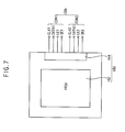
- FIG. 7 is a plan view illustrating a control logic substrate of the light source control unit illustrated in FIG. 4 . As indicated, ground lines are not shown.
- control logic substrate 160 may include a control logic element 162 and a control logic connector 164 .
- the control logic element 162 generates a plurality of control signals CON for controlling the currents control element 126 .
- the control logic element 162 may output the control signals CON in response to one or more logic control signals applied from an exterior source (not shown).
- the control logic element 162 may be a field programmable gate array (FPGA).
- the control logic connector 164 is electrically connected to the control logic element 162 to receive the control signals CON.
- the control logic connector 164 is electrically connected to the light source driving connector 128 through the control logic cable 134 to output the control signals CON.
- the control signals CON may include a first control signals set CON 1 for controlling the first currents control element 126 a and a second control signals set CON 2 for controlling the second currents control element 126 b.
- the first control signals set CON 1 may include a first clock signal CLK 1 , a first data signal DATA 1 , a first latch-enable control signal LE 1 and a first output-enable control signal OE 1 .
- the second control signals set CON 2 may include a second clock signal CLK 2 , a second data signal DATA 2 , a second latch-enable control signal LE 2 and a second output-enable control signal OE 2 .
- FIG. 8 is a plan view schematically illustrating the light source module of FIG. 4 .
- the lower half is vertically flipped so as to result in a symmetrical disposition with power lines (e.g., Vd 1 , VD 2 ) on the outside of the board and control lines (e.g., data, clock) running more to the center of the board.
- power lines e.g., Vd 1 , VD 2
- control lines e.g., data, clock
- the first and second driving voltages Vd 1 and Vd 2 generated in the power supply substrate 150 are applied to the light source driving connector 128 through the power supply cable 132
- the first and second control signal sets CON 1 and CON 2 generated in the control logic substrate 160 are applied to the light source driving connector 128 through the control logic cable 134 .
- the light source driving connector 128 is electrically connected to the first currents control subelement 126 a to apply the first control signals set CON 1 , and is electrically connected to the second currents control subelement 126 b to apply the second control signals set CON 2 .
- the light source driving connector 128 is electrically connected to each first terminal of the light source blocks BL arranged in the first row to apply thereto the first driving voltage Vd 1 , and is electrically connected to each first terminal of the light source blocks BL arranged in the second row to apply thereto the second driving voltage Vd 2 .
- the light sources 124 e.g., LEDs
- the light sources 124 included in each of the light source blocks BL are electrically connected to each other as three series circuits, for example one constituted by red light emitting LEDs, one constituted by green light emitting LEDs and one constituted by blue light emitting LEDs so that the combination of primary colors appears as a white light.
- Channel terminals of the first currents control subelements 126 a are electrically connected to respective second terminals of the light source blocks BL arranged in the first row, and may individually control the first driving currents applied to the light source blocks BL arranged in the first row.
- a first channel terminal CH 1 of the first currents control element 126 a is electrically connected to a second terminal of the light source block BL arranged in the first column and the first row.
- a second channel terminal CH 2 of the first currents control element 126 a is electrically connected to a second terminal of the light source block BL arranged in the second column and the first row
- a third channel terminal CH 3 of the first currents control element 126 a is electrically connected to a second terminal of the light source block BL arranged in the third column and the first row.
- Channel terminals of the second currents control elements 126 b are electrically connected to respective second terminals of the light source blocks BL arranged in the second row, and may individually control the second driving currents applied to the light source blocks BL arranged in the second row.
- a first channel terminal CH 1 of the second currents control element 126 b is electrically connected to a second terminal of the light source block BL arranged in the first column and the second row.
- a second channel terminal CH 2 of the second currents control element 126 b is electrically connected to a second terminal of the light source block BL arranged in the second column and the second row
- a third channel terminal CH 3 of the second currents control element 126 b is electrically connected to a second terminal of the light source block BL arranged in the third column and the second row.
- FIG. 9 is a plan view illustrating an electrical connection between a light source module having another light source and a light source control unit of a backlight assembly in accordance with further still another embodiment.
- FIG. 10 is a plan view illustrating the light source module of FIG. 9 .
- ground lines and other ancillary electrical structures are not shown so as to avoid illustrative clutter.
- the backlight assembly illustrated in FIGS. 9 and 10 may have substantially the same structure as the backlight assembly described with reference to FIGS. 4 and 8 except for a kind of a light source and a structure of a light source module.
- the same reference number is used for the same or similar element, and any further descriptions concerning the same or similar elements as those described in FIGS. 4 and 8 will be omitted here.
- each of light source blocks BL includes at least one light source 124 .
- the light source 124 may include one or more red light emitting diodes RD, one or more green light emitting diodes GD and one or more blue light emitting diodes BD.
- the number of RGB light sources 124 included in each of the light source blocks BL of FIG. 9 is four, and the four RGB light sources 124 may be arranged in two columns and two rows along the first and second directions D 1 and D 2 .
- the number of the white light sources 124 and an arranging relationship of the light sources 124 are different from those in FIG. 9 .
- the red light emitting diodes RD included in each of the light source blocks BL are electrically connected to each other in series to form a red light emitting string.
- the green light emitting diodes GD included in each of the light source blocks BL are electrically connected to each other in series to form a green light emitting string
- the blue light emitting diodes BD included in each of the light source blocks BL are electrically connected to each other in series to form a blue light emitting string.
- the first and second currents control subelements 126 a and 126 b may individually control each of the red, green and blue light emitting strings that are included in one light source block BL.
- the currents controlling element 126 is disposed on the driving substrate 122 as opposed to being disposed on the power supply substrate 150 .
- the number of wires of the connection cable 130 connected to the light source driving connector 128 and the number of pins of the light source driving connector 128 may be substantially smaller than the number of lines needed for independently driving the LED current strings.
- connection cable 130 between the LCU (see FIG. 1 ) and the light sources supporting board (e.g., 122 of FIG. 1 ) does not need to contain as many independent lines as there are independent current strings in need of independent control. That is, the number of the wires of the connection cable 130 do not need to be increased as the number of the channel terminals of the currents control element 126 increases.
- connection cable 130 When the number of the wires of the connection cable 130 is reduced, the cost of the connection cable 130 may be reduced, and the risk of contact defect between the disconnectably connectable connection cable 130 and the light source driving connector 128 may be reduced due to the reduced number of disconnectably connectable contact pins.
- FIG. 11 is a cross-sectional view illustrating a display device in accordance with further still other embodiment.
- the display device illustrated in FIG. 11 may have substantially the same structure as the display devices described with reference to FIGS. 1 to 3 except that the display device illustrated in FIG. 11 has a light source control unit (LCU) on a sliding substrate that is directly connectable to the light source driving connector without use of an intermediate connection cable.
- LCU light source control unit
- the light source driving connector 128 is disposed on the second side of the driving substrate 122 facing the bottom plate 112 of the receiving container 110 .
- the light source driving connector 128 may be disposed at an end portion of the second side of the driving substrate 122 corresponding to the currents control element 126 .
- the bottom plate 112 of the receiving container 110 may have a connector receiving hole 112 a for receiving the light source driving connector 128 .
- the light source driving connector 128 protrudes downwardly from the bottom plate 112 through the connector receiving hole 112 a .
- the light source driving connector 128 may include a receiving groove to combine with the light source control unit LCU directly or with a printed circuit substrate that supports the LCU and has an edge connector adapted to mate with the light source driving connector 128 .
- the receiving groove may be formed at the portion protruding down from the bottom plate 112 .
- the light source control unit LCU may be slidingly inserted into the receiving groove of the light source driving connector 128 , and electrically connected to the light source driving connector 128 .
- the light source control unit LCU may include one or more metal patterns formed on a substrate thereof for electrically connecting with the light source driving connector 128 .
- the number of light source control units (LCU's, two shown) used in the embodiment of FIG. 11 may correspond with the number of the light source modules 120 that are to be controlled. For example, when the number of the light source modules 120 is four, the number of the light source control units LCU may be four. Alternatively, one light source control unit LCU may control two light source modules 120 , or one light source control unit LCU may control all four light source modules 120 together.
- one among the light source modules 120 may be electrically connected to the light source control unit LCU, and the others of the light source modules 120 may be internally connected to each other or may be electrically connected to each other via some connecting members.
Abstract
Description
Claims (30)
Applications Claiming Priority (2)
| Application Number | Priority Date | Filing Date | Title |
|---|---|---|---|
| KR10-2007-0113456 | 2007-11-08 | ||
| KR1020070113456A KR101410496B1 (en) | 2007-11-08 | 2007-11-08 | Light source module, back light assembly having the light source module and display apparatus having the back light assembly |
Publications (2)
| Publication Number | Publication Date |
|---|---|
| US20090121652A1 US20090121652A1 (en) | 2009-05-14 |
| US7956544B2 true US7956544B2 (en) | 2011-06-07 |
Family
ID=40623075
Family Applications (1)
| Application Number | Title | Priority Date | Filing Date |
|---|---|---|---|
| US12/102,684 Active 2029-02-11 US7956544B2 (en) | 2007-11-08 | 2008-04-14 | Light source module, backlight assembly having the same, display device having the same and method for reducing number of wires used in interconnect cable of the same |
Country Status (2)
| Country | Link |
|---|---|
| US (1) | US7956544B2 (en) |
| KR (1) | KR101410496B1 (en) |
Cited By (4)
| Publication number | Priority date | Publication date | Assignee | Title |
|---|---|---|---|---|
| US20090141210A1 (en) * | 2007-11-29 | 2009-06-04 | Cho Joo-Woan | Light source block assembly and backlight unit and liquid crystal display having the same |
| US20120170265A1 (en) * | 2009-09-17 | 2012-07-05 | Koninklijke Philips Electronics N.V. | Light-source module and light-emitting device |
| US20130229802A1 (en) * | 2010-12-01 | 2013-09-05 | Sharp Kabushiki Kaisha | Planar light-emitting illumination device |
| US11227556B1 (en) | 2020-12-03 | 2022-01-18 | Samsung Electronics Co., Ltd. | Display apparatus and light apparatus thereof |
Families Citing this family (23)
| Publication number | Priority date | Publication date | Assignee | Title |
|---|---|---|---|---|
| US8164281B2 (en) * | 2008-08-01 | 2012-04-24 | Thomas Warton | Luminaire system and method |
| KR101014935B1 (en) * | 2009-06-15 | 2011-02-15 | 김명일 | The LED Lighting utilized The Diffuser plate |
| KR101601087B1 (en) * | 2009-10-14 | 2016-03-09 | 엘지디스플레이 주식회사 | Backlight unit liquid crystal display device including the same and method of driving the same |
| EP2508789A4 (en) * | 2009-12-02 | 2013-12-04 | Sharp Kk | Illumination device, and display device |
| JP5100823B2 (en) * | 2010-06-25 | 2012-12-19 | 日本航空電子工業株式会社 | Backlight assembly, backlight unit, and liquid crystal display device |
| TW201327515A (en) * | 2011-12-30 | 2013-07-01 | Au Optronics Corp | LED module |
| CO6820274A1 (en) * | 2012-06-26 | 2013-12-31 | Velez Juan Camilo Diaz | LED light of ultra low consumption multiplexed |
| CN102750911B (en) * | 2012-07-10 | 2015-11-25 | 深圳市华星光电技术有限公司 | A kind of LED backlight drive circuit, backlight module and liquid crystal indicator |
| CN103347327B (en) * | 2013-06-14 | 2016-07-13 | 昆山龙腾光电有限公司 | Light-emitting diode driving board, display floater drive plate and display device |
| US9974125B2 (en) * | 2015-07-17 | 2018-05-15 | Cooper Technologies Company | Modular integrated lighting circuit |
| WO2017038080A1 (en) | 2015-09-01 | 2017-03-09 | パナソニックIpマネジメント株式会社 | Video display device |
| US10643556B2 (en) | 2015-09-01 | 2020-05-05 | Panasonic Intellectual Property Management Co., Ltd. | Video display device |
| US10663793B2 (en) | 2015-09-01 | 2020-05-26 | Panasonic Intellectual Property Management Co., Ltd. | Image display device |
| JP6634612B2 (en) | 2015-09-01 | 2020-01-22 | パナソニックIpマネジメント株式会社 | Video display device |
| WO2017038083A1 (en) | 2015-09-01 | 2017-03-09 | パナソニックIpマネジメント株式会社 | Image display device |
| EP3346322B1 (en) | 2015-09-01 | 2020-09-30 | Panasonic Intellectual Property Management Co., Ltd. | Video display device |
| CN106383419A (en) * | 2016-08-29 | 2017-02-08 | 合肥惠科金扬科技有限公司 | Light source fixing device of straight-down backlight module set |
| CN106125401A (en) * | 2016-08-29 | 2016-11-16 | 合肥惠科金扬科技有限公司 | A kind of light source fixing device processing method of down straight aphototropism mode set |
| US11705440B2 (en) * | 2017-06-26 | 2023-07-18 | PlayNitride Inc. | Micro LED display panel |
| US20190250462A1 (en) * | 2018-02-12 | 2019-08-15 | Innolux Corporation | Display device |
| US11116051B1 (en) * | 2018-07-12 | 2021-09-07 | Leimac Ltd. | Dimming power supply device and light source device |
| US11016339B2 (en) * | 2019-08-28 | 2021-05-25 | Wuhan China Star Optoelectronics Technology Co., Ltd. | Backlight module and in vehicle display device |
| KR102536474B1 (en) * | 2021-04-13 | 2023-05-26 | 주식회사 엠알케이 | High-brightness display device with improved cooling efficiency |
Citations (11)
| Publication number | Priority date | Publication date | Assignee | Title |
|---|---|---|---|---|
| KR20060014575A (en) | 2004-08-11 | 2006-02-16 | 주식회사 한국싸인 | Combination structure of a led module |
| KR20060038556A (en) | 2004-10-30 | 2006-05-04 | 엘지.필립스 엘시디 주식회사 | Apparatus of light emitting diode backlight and liquid crystal display device using thereof |
| US20060221592A1 (en) * | 2005-03-31 | 2006-10-05 | Sony Corporation | Light-emitting diode device and backlight apparatus and liquid-crystal display apparatus using light-emitting diode device |
| US20060221612A1 (en) * | 2005-03-29 | 2006-10-05 | Samsung Electronics Co., Ltd. | Backlight unit and liquid crystal display having the same |
| JP2006285181A (en) | 2005-03-09 | 2006-10-19 | Masao Yoshida | Ultra slim high-luminance light panel |
| US20080030645A1 (en) * | 2006-08-03 | 2008-02-07 | Samsung Electronics Co., Ltd. | Light emitting unit, backlight assembly, and display apparatus having the same |
| US7495397B2 (en) * | 2006-06-01 | 2009-02-24 | Sony Corporation | Drive device for light emitting diode element, light source device, and display |
| US7541752B2 (en) * | 2005-06-21 | 2009-06-02 | Toshiba Matsushita Display Technology Co., Ltd. | Illuminating device and liquid crystal display |
| US7566143B2 (en) * | 2006-05-30 | 2009-07-28 | Sony Corporation | Backlight apparatus and color image display apparatus |
| US7573447B2 (en) * | 2004-05-28 | 2009-08-11 | Lg Display Co., Ltd. | Apparatus and method for driving liquid crystal display device |
| US7683981B2 (en) * | 2006-02-23 | 2010-03-23 | Samsung Electronics Co., Ltd. | Light emitting diode substrate, method of manufacturing the same, and liquid crystal display device using the same |
-
2007
- 2007-11-08 KR KR1020070113456A patent/KR101410496B1/en active IP Right Grant
-
2008
- 2008-04-14 US US12/102,684 patent/US7956544B2/en active Active
Patent Citations (11)
| Publication number | Priority date | Publication date | Assignee | Title |
|---|---|---|---|---|
| US7573447B2 (en) * | 2004-05-28 | 2009-08-11 | Lg Display Co., Ltd. | Apparatus and method for driving liquid crystal display device |
| KR20060014575A (en) | 2004-08-11 | 2006-02-16 | 주식회사 한국싸인 | Combination structure of a led module |
| KR20060038556A (en) | 2004-10-30 | 2006-05-04 | 엘지.필립스 엘시디 주식회사 | Apparatus of light emitting diode backlight and liquid crystal display device using thereof |
| JP2006285181A (en) | 2005-03-09 | 2006-10-19 | Masao Yoshida | Ultra slim high-luminance light panel |
| US20060221612A1 (en) * | 2005-03-29 | 2006-10-05 | Samsung Electronics Co., Ltd. | Backlight unit and liquid crystal display having the same |
| US20060221592A1 (en) * | 2005-03-31 | 2006-10-05 | Sony Corporation | Light-emitting diode device and backlight apparatus and liquid-crystal display apparatus using light-emitting diode device |
| US7541752B2 (en) * | 2005-06-21 | 2009-06-02 | Toshiba Matsushita Display Technology Co., Ltd. | Illuminating device and liquid crystal display |
| US7683981B2 (en) * | 2006-02-23 | 2010-03-23 | Samsung Electronics Co., Ltd. | Light emitting diode substrate, method of manufacturing the same, and liquid crystal display device using the same |
| US7566143B2 (en) * | 2006-05-30 | 2009-07-28 | Sony Corporation | Backlight apparatus and color image display apparatus |
| US7495397B2 (en) * | 2006-06-01 | 2009-02-24 | Sony Corporation | Drive device for light emitting diode element, light source device, and display |
| US20080030645A1 (en) * | 2006-08-03 | 2008-02-07 | Samsung Electronics Co., Ltd. | Light emitting unit, backlight assembly, and display apparatus having the same |
Cited By (10)
| Publication number | Priority date | Publication date | Assignee | Title |
|---|---|---|---|---|
| US20090141210A1 (en) * | 2007-11-29 | 2009-06-04 | Cho Joo-Woan | Light source block assembly and backlight unit and liquid crystal display having the same |
| US8197082B2 (en) * | 2007-11-29 | 2012-06-12 | Samsung Electronics Co., Ltd. | Light source block assembly and backlight unit and liquid crystal display having the same |
| US20120170265A1 (en) * | 2009-09-17 | 2012-07-05 | Koninklijke Philips Electronics N.V. | Light-source module and light-emitting device |
| US9743521B2 (en) * | 2009-09-17 | 2017-08-22 | Philips Lighting Holding B.V. | Light-source module and light-emitting device |
| US20130229802A1 (en) * | 2010-12-01 | 2013-09-05 | Sharp Kabushiki Kaisha | Planar light-emitting illumination device |
| US11227556B1 (en) | 2020-12-03 | 2022-01-18 | Samsung Electronics Co., Ltd. | Display apparatus and light apparatus thereof |
| US11373605B1 (en) | 2020-12-03 | 2022-06-28 | Samsung Electronics Co., Ltd. | Display apparatus and light apparatus thereof |
| US11410619B2 (en) | 2020-12-03 | 2022-08-09 | Samsung Electronics Co., Ltd. | Display apparatus and light apparatus thereof |
| US11417287B2 (en) | 2020-12-03 | 2022-08-16 | Samsung Electronics Co., Ltd. | Display apparatus and light apparatus thereof |
| US11837182B2 (en) | 2020-12-03 | 2023-12-05 | Samsung Electronics Co., Ltd. | Display apparatus and light apparatus thereof |
Also Published As
| Publication number | Publication date |
|---|---|
| KR101410496B1 (en) | 2014-06-20 |
| US20090121652A1 (en) | 2009-05-14 |
| KR20090047568A (en) | 2009-05-13 |
Similar Documents
| Publication | Publication Date | Title |
|---|---|---|
| US7956544B2 (en) | Light source module, backlight assembly having the same, display device having the same and method for reducing number of wires used in interconnect cable of the same | |
| US20190289687A1 (en) | Microled display panel | |
| US8289267B2 (en) | Backlight assembly and display apparatus having the same | |
| EP1947490B1 (en) | Backlight assembly and cover for a compact display apparatus | |
| US7744233B2 (en) | Backlight device and liquid crystal display device | |
| US7812810B2 (en) | Inverter driving apparatus and liquid crystal display including inverter driving apparatus | |
| US20100188438A1 (en) | Backlight and Liquid Crystal Display Device | |
| US7724340B2 (en) | Liquid crystal display panel having power supply lines and liquid crystal display | |
| US20070200121A1 (en) | Multi-colored LED array with improved color uniformity | |
| US20100123741A1 (en) | Method of driving a light source, light source apparatus for performing the method and display apparatus having the light source apparatus | |
| KR102544236B1 (en) | Back light unit and liquid crystal display device having the same | |
| US20080111502A1 (en) | Backlight assembly and method of driving the same | |
| US8294660B2 (en) | Blacklight unit and display device including the same | |
| US20090122544A1 (en) | Backlight assembly and display device having the same | |
| US8093827B2 (en) | Light source module, light source assembly having the same and display device having the light source module | |
| US20210096423A1 (en) | Display device | |
| KR20120036660A (en) | Backlight unit and liquid crystal display including the same | |
| US20070132707A1 (en) | Display device and method of driving the same | |
| CN111103726B (en) | Backlight, display device and backlight control method | |
| CN112965306B (en) | Display panel and display device | |
| US20090146943A1 (en) | Light source module, display device having the same, and a method thereof | |
| US20240127747A1 (en) | Compensation circuit and driving circuit of light-emitting elements, and led display device | |
| US11963429B2 (en) | Display module and display apparatus | |
| US20230180589A1 (en) | Display module and display apparatus | |
| KR20090035135A (en) | Backlight unit for liquid crystal display device |
Legal Events
| Date | Code | Title | Description |
|---|---|---|---|
| AS | Assignment |
Owner name: SAMSUNG ELECTRONICS CO., LTD., KOREA, REPUBLIC OF Free format text: ASSIGNMENT OF ASSIGNORS INTEREST;ASSIGNORS:KANG, EUI-JEONG;KIM, GI-CHERL;PARK, SE-KI;REEL/FRAME:020801/0332 Effective date: 20080411 |
|
| FEPP | Fee payment procedure |
Free format text: PAYOR NUMBER ASSIGNED (ORIGINAL EVENT CODE: ASPN); ENTITY STATUS OF PATENT OWNER: LARGE ENTITY |
|
| STCF | Information on status: patent grant |
Free format text: PATENTED CASE |
|
| AS | Assignment |
Owner name: SAMSUNG DISPLAY CO., LTD, KOREA, REPUBLIC OF Free format text: ASSIGNMENT OF ASSIGNORS INTEREST;ASSIGNOR:SAMSUNG ELECTRONICS, CO., LTD;REEL/FRAME:028990/0336 Effective date: 20120904 |
|
| FPAY | Fee payment |
Year of fee payment: 4 |
|
| MAFP | Maintenance fee payment |
Free format text: PAYMENT OF MAINTENANCE FEE, 8TH YEAR, LARGE ENTITY (ORIGINAL EVENT CODE: M1552); ENTITY STATUS OF PATENT OWNER: LARGE ENTITY Year of fee payment: 8 |
|
| MAFP | Maintenance fee payment |
Free format text: PAYMENT OF MAINTENANCE FEE, 12TH YEAR, LARGE ENTITY (ORIGINAL EVENT CODE: M1553); ENTITY STATUS OF PATENT OWNER: LARGE ENTITY Year of fee payment: 12 |