US8042260B2 - Methods of forming inductors on integrated circuits - Google Patents

Methods of forming inductors on integrated circuits Download PDF

Info

Publication number
US8042260B2
US8042260B2 US12/250,385 US25038508A US8042260B2 US 8042260 B2 US8042260 B2 US 8042260B2 US 25038508 A US25038508 A US 25038508A US 8042260 B2 US8042260 B2 US 8042260B2
Authority
US
United States
Prior art keywords
core elements
forming
core
substrate
isolation
Prior art date
Legal status (The legal status is an assumption and is not a legal conclusion. Google has not performed a legal analysis and makes no representation as to the accuracy of the status listed.)
Active, expires
Application number
US12/250,385
Other versions
US20090038142A1 (en
Inventor
Peter J. Hopper
Peter Johnson
Peter Smeys
Andrei Papou
Current Assignee (The listed assignees may be inaccurate. Google has not performed a legal analysis and makes no representation or warranty as to the accuracy of the list.)
National Semiconductor Corp
Original Assignee
National Semiconductor Corp
Priority date (The priority date is an assumption and is not a legal conclusion. Google has not performed a legal analysis and makes no representation as to the accuracy of the date listed.)
Filing date
Publication date
Application filed by National Semiconductor Corp filed Critical National Semiconductor Corp
Priority to US12/250,385 priority Critical patent/US8042260B2/en
Assigned to NATIONAL SEMICONDUCTOR CORPORATION reassignment NATIONAL SEMICONDUCTOR CORPORATION ASSIGNMENT OF ASSIGNORS INTEREST (SEE DOCUMENT FOR DETAILS). Assignors: HOPPER, PETER J., SMEYS, PETER, JOHNSON, PETER, PAPOU, ANDREI
Publication of US20090038142A1 publication Critical patent/US20090038142A1/en
Application granted granted Critical
Publication of US8042260B2 publication Critical patent/US8042260B2/en
Active legal-status Critical Current
Adjusted expiration legal-status Critical

Links

Images

Classifications

    • HELECTRICITY
    • H01ELECTRIC ELEMENTS
    • H01LSEMICONDUCTOR DEVICES NOT COVERED BY CLASS H10
    • H01L23/00Details of semiconductor or other solid state devices
    • H01L23/52Arrangements for conducting electric current within the device in operation from one component to another, i.e. interconnections, e.g. wires, lead frames
    • H01L23/522Arrangements for conducting electric current within the device in operation from one component to another, i.e. interconnections, e.g. wires, lead frames including external interconnections consisting of a multilayer structure of conductive and insulating layers inseparably formed on the semiconductor body
    • H01L23/5227Inductive arrangements or effects of, or between, wiring layers
    • HELECTRICITY
    • H01ELECTRIC ELEMENTS
    • H01FMAGNETS; INDUCTANCES; TRANSFORMERS; SELECTION OF MATERIALS FOR THEIR MAGNETIC PROPERTIES
    • H01F17/00Fixed inductances of the signal type 
    • H01F17/0006Printed inductances
    • HELECTRICITY
    • H01ELECTRIC ELEMENTS
    • H01FMAGNETS; INDUCTANCES; TRANSFORMERS; SELECTION OF MATERIALS FOR THEIR MAGNETIC PROPERTIES
    • H01F41/00Apparatus or processes specially adapted for manufacturing or assembling magnets, inductances or transformers; Apparatus or processes specially adapted for manufacturing materials characterised by their magnetic properties
    • H01F41/02Apparatus or processes specially adapted for manufacturing or assembling magnets, inductances or transformers; Apparatus or processes specially adapted for manufacturing materials characterised by their magnetic properties for manufacturing cores, coils, or magnets
    • H01F41/04Apparatus or processes specially adapted for manufacturing or assembling magnets, inductances or transformers; Apparatus or processes specially adapted for manufacturing materials characterised by their magnetic properties for manufacturing cores, coils, or magnets for manufacturing coils
    • H01F41/041Printed circuit coils
    • H01F41/046Printed circuit coils structurally combined with ferromagnetic material
    • HELECTRICITY
    • H01ELECTRIC ELEMENTS
    • H01LSEMICONDUCTOR DEVICES NOT COVERED BY CLASS H10
    • H01L2924/00Indexing scheme for arrangements or methods for connecting or disconnecting semiconductor or solid-state bodies as covered by H01L24/00
    • H01L2924/0001Technical content checked by a classifier
    • H01L2924/0002Not covered by any one of groups H01L24/00, H01L24/00 and H01L2224/00
    • YGENERAL TAGGING OF NEW TECHNOLOGICAL DEVELOPMENTS; GENERAL TAGGING OF CROSS-SECTIONAL TECHNOLOGIES SPANNING OVER SEVERAL SECTIONS OF THE IPC; TECHNICAL SUBJECTS COVERED BY FORMER USPC CROSS-REFERENCE ART COLLECTIONS [XRACs] AND DIGESTS
    • Y10TECHNICAL SUBJECTS COVERED BY FORMER USPC
    • Y10TTECHNICAL SUBJECTS COVERED BY FORMER US CLASSIFICATION
    • Y10T29/00Metal working
    • Y10T29/49Method of mechanical manufacture
    • Y10T29/49002Electrical device making
    • Y10T29/4902Electromagnet, transformer or inductor
    • Y10T29/49071Electromagnet, transformer or inductor by winding or coiling
    • YGENERAL TAGGING OF NEW TECHNOLOGICAL DEVELOPMENTS; GENERAL TAGGING OF CROSS-SECTIONAL TECHNOLOGIES SPANNING OVER SEVERAL SECTIONS OF THE IPC; TECHNICAL SUBJECTS COVERED BY FORMER USPC CROSS-REFERENCE ART COLLECTIONS [XRACs] AND DIGESTS
    • Y10TECHNICAL SUBJECTS COVERED BY FORMER USPC
    • Y10TTECHNICAL SUBJECTS COVERED BY FORMER US CLASSIFICATION
    • Y10T29/00Metal working
    • Y10T29/49Method of mechanical manufacture
    • Y10T29/49002Electrical device making
    • Y10T29/4902Electromagnet, transformer or inductor
    • Y10T29/49073Electromagnet, transformer or inductor by assembling coil and core
    • YGENERAL TAGGING OF NEW TECHNOLOGICAL DEVELOPMENTS; GENERAL TAGGING OF CROSS-SECTIONAL TECHNOLOGIES SPANNING OVER SEVERAL SECTIONS OF THE IPC; TECHNICAL SUBJECTS COVERED BY FORMER USPC CROSS-REFERENCE ART COLLECTIONS [XRACs] AND DIGESTS
    • Y10TECHNICAL SUBJECTS COVERED BY FORMER USPC
    • Y10TTECHNICAL SUBJECTS COVERED BY FORMER US CLASSIFICATION
    • Y10T29/00Metal working
    • Y10T29/49Method of mechanical manufacture
    • Y10T29/49002Electrical device making
    • Y10T29/4902Electromagnet, transformer or inductor
    • Y10T29/49075Electromagnet, transformer or inductor including permanent magnet or core
    • YGENERAL TAGGING OF NEW TECHNOLOGICAL DEVELOPMENTS; GENERAL TAGGING OF CROSS-SECTIONAL TECHNOLOGIES SPANNING OVER SEVERAL SECTIONS OF THE IPC; TECHNICAL SUBJECTS COVERED BY FORMER USPC CROSS-REFERENCE ART COLLECTIONS [XRACs] AND DIGESTS
    • Y10TECHNICAL SUBJECTS COVERED BY FORMER USPC
    • Y10TTECHNICAL SUBJECTS COVERED BY FORMER US CLASSIFICATION
    • Y10T29/00Metal working
    • Y10T29/49Method of mechanical manufacture
    • Y10T29/49002Electrical device making
    • Y10T29/49117Conductor or circuit manufacturing
    • Y10T29/49124On flat or curved insulated base, e.g., printed circuit, etc.
    • Y10T29/4913Assembling to base an electrical component, e.g., capacitor, etc.

Definitions

  • the present invention relates to wafer level fabrication of high value inductors on semiconductor integrated circuits, and more particularly, to the optimization of power inductor arrays on integrated circuits for switching regulator applications.
  • Inductors are commonly used in the electronics industry for storing magnetic energy. Providing an electric current though a metal conductor, such as a metal plate or bar, typically creates an inductor. The current passing though the metal conductor creates a magnetic field or flux around the conductor. The amount of inductance is measured in terms of Henries. In the semiconductor industry, it is known to form inductors on integrated circuits. The inductors are typically created by fabricating what is commonly called an “air coil” inductor on the chip. The air coil inductor is usually either aluminum or some other metal patterned in a helical, toroidal or a “watch spring” coil shape. By applying a current through the inductor, the magnetic flux is created.
  • Inductors are used on chips for a number of applications. Perhaps the most common application is DC-to-DC switching regulators. In many situations, however, on chip inductors do not generate enough flux or energy for a particular application. When this occurs, very often an off-chip discrete inductor is used.
  • Off-chip inductors There are a number of problems in using off-chip inductors. Foremost, they tend to be expensive. With advances in semiconductor process technology, millions upon millions of transistors can be fabricated onto a single chip. With all these transistors, designers have been able to cram a tremendous amount of functionality onto a single chip and an entire system on just one or a handful of chips. Providing an off-chip inductor can therefore be relatively expensive compared to the overall cost of the system. Off-chip inductors can also be problematic in situations where space is at a premium. In a cell phone or personal digital assistant (PDA) for example, it may be difficult to squeeze a discrete inductor into a compact package. As a result, the consumer product may not be as small or compact as desired.
  • PDA personal digital assistant
  • the claimed invention pertains to methods of forming one or more inductors on a semiconductor substrate.
  • a method of forming an array of inductor core elements on a semiconductor substrate that includes integrated circuits is disclosed.
  • a first set of spaced apart metallic core elements are formed over the substrate. Isolation sidewalls are then formed on side surfaces of the core elements.
  • a second set of metallic core elements are formed over the substrate.
  • at least one core element of the second set of core elements is positioned in a space between an associated adjacent pair of core elements from the first set of core elements.
  • the first and second sets of core elements are substantially co-planar and interleaved such that only the isolation sidewalls separate adjacent core elements.
  • a metal seed layer is formed over a semiconductor substrate.
  • a layer of photoresist is deposited over the metal seed layer.
  • the photoresist is patterned using lithographic techniques to form recesses in the photoresist that expose portions of the metal seed layer.
  • a first metal material is electroplated into the recesses to form a first set of spaced apart core elements.
  • a conformal isolation layer is deposited over the substrate after the first set of core elements have been formed so that the isolation layer covers surfaces of the core elements and regions between the core elements. As a result, isolation sidewalls are formed on each of the core elements. Portions of the isolation layer that cover regions between core elements are etched away to expose portions of the metal seed layer without removing the isolation sidewalls.
  • a second metal material is electroplated after the isolation layer etching to form a second set of metallic core elements.
  • the first and second sets of core elements are substantially co-planar and interleaved such that only the isolation sidewalls separate adjacent core elements.
  • FIG. 1A is a block diagram of power regulator system.
  • FIG. 1B is a circuit diagram of a power regulator circuit.
  • FIGS. 2A is a plot illustrating the relationship between flux density versus magnetic field intensity in the inductor and core of the power regulator circuit of FIG. 1B .
  • FIG. 2B a plot illustrating the relationship between the inductance and the current in the coil of the power regulator circuit of FIG. 1B .
  • FIG. 3 is a block diagram of a semiconductor chip having a power regulator circuit fabricated thereon according to the present invention.
  • FIGS. 4A through 4D illustrate various embodiments of a core array of the power regulator circuit according to the present invention.
  • FIG. 5 illustrates a cross section of a core element of the core array according to the present invention.
  • FIG. 6A is a block diagram of the phase control circuit used in the regulator circuit of the present invention.
  • FIG. 6B is a diagram showing an output signal at the output node of the regulator circuit of the present invention.
  • FIGS. 7A-7H are a sequence of cross sections of a semiconductor chip illustrating the sequence of fabricating core elements of the core array used in the regulator circuit of the present invention.
  • the system 10 includes a regulator circuit 12 and a controller 14 coupled between a power supply 16 and a device 18 , such as micro-controller, that requires a steady direct current (DC) voltage.
  • the regulator circuit 12 includes an inductor (L) and a core (both not illustrated).
  • the input voltage Vin is typically a pulsed input signal from the power supply 16 having a frequency (f) and an amplitude equal to Vin. With each positive and negative pulse transition, the inductor is cyclically energized and then de-energized, causing the flux in the core to increase and then decrease respectively.
  • the output Vout of the regulator circuit 12 is coupled to the device 18 .
  • the controller 14 causes the frequency (i.e., sometimes referred to as the duty cycle) of the pulses of the input voltage Vin to either increase or decrease as needed to maintain a steady output voltage.
  • the circuit 12 includes two transistors T 1 and T 2 with their channels coupled in series between Vcc and ground.
  • a first capacitor C 1 is also coupled between Vcc and ground in parallel with the channels of transistors T 1 and T 2 .
  • One end of the inductor coil L is coupled between the two transistors T 1 and T 2 and the opposite end is coupled to the output node Vout.
  • a core 20 is provided adjacent the inductor L.
  • a second capacitor C 2 is coupled between the output node Vout and ground.
  • the gate of transistor T 1 is coupled to receive the pulsed input signal Vin.
  • the gate of transistor T 2 is coupled to receive the complement of signal Vin.
  • the regulator circuit 12 operates in alternating high and low phases.
  • a positive voltage pulse of Vin is applied to the gate of transistor T 1
  • a complementary or negative pulse is applied to the gate of transistor T 2 .
  • This causes transistor T 1 to turn on and transistor T 2 to turn off.
  • transistor T 1 on current is pulled through transistor T 1 from Vcc to energize the coil of inductor L, creating a flux in the core 20 .
  • the low phase occurs when the input pulse transitions low at the gate of transistor T 1 and high at the gate of transistor T 2 . When this occurs, the transistor T 1 turns off and transistor T 2 turns on.
  • the inductor L pulls current from ground through transistor T 2 , causing the inductor to de-energize and the flux in the core 20 to collapse.
  • the aforementioned cycle is repeated with each pulse of Vin and the complement is applied to transistors T 1 and T 2 .
  • the output of the circuit 12 is ideally a steady voltage. Due to the cyclical increases and decreases of the energy in the inductor L and the flux in the core 20 , the output voltage Vout will typically have a ripple.
  • the output capacitor C 2 is provided to smooth out the ripple.
  • FIG. 2A a plot illustrating the relationship between the flux density as measured in Webers per cm 2 (B) versus the magnetic field intensity as measured in ampere turns per meter (H) in the inductor L and core 20 is shown.
  • B the flux density
  • H the magnetic field intensity
  • Bsat the magnetic field intensity
  • the slope of the plot or curve, calculated by B/H defines the permeability (i.e., the propensity) of the material of the core 20 to become magnetized. Bsat is thus defined as the point where the maximum state of magnetization or flux of the material of the core 20 is achieved.
  • Bsat flux density saturation point
  • Iron has a high level of permeability
  • other materials such as FeNi (permalloy) have a relatively low permeability.
  • FIG. 2B a plot illustrating the relationship between the inductance (L) and the current (I) in the coil L is shown.
  • the inductance L With a relatively small current, the inductance L is high. As the current increases, the inductance L drops off until the saturation point Lsat is reached.
  • FIG. 2B represents the derivative of H and B, and is plotting the slope of FIG. 2A . Inductance then, relates to the derivative of B and H or in other words is proportional to the permeability. The inductance rolls off at the point following the magnetic saturation of the core material.
  • the integrated circuit 30 includes a plurality of regulator circuits 32 each having an input node 34 configured to receive complementary pulsed input signals 36 respectively (for the sake of simplicity, only the positive pulsed signal is shown).
  • a plurality of inductor core windings 38 is associated with each of the plurality of regulator circuits 32 .
  • the regulator circuits 32 are each identical to that illustrated in FIG. 1B with the exception of the core 20 . Rather than a specific core 20 associated with each circuit 32 , an engineered distributed core array 40 is provided for all of the regulator circuits 32 .
  • the core array 40 including a plurality of core elements (not illustrated), is positioned adjacent to and is magnetically coupled to each of the inductor windings 38 .
  • An output node 42 is electrically coupled to the plurality of inductor windings 42 .
  • a phase control circuit connected between the output node 42 and the regulator circuits 32 , is provided to control the phase of each of the input signals 36 .
  • the general principle of the present invention is the combined use of phased multiple driver circuits 32 , each driving one or more core elements of the core array 40 .
  • energy storage can be maximized while minimizing core losses.
  • FIG. 3 is figurative in the sense that it shows the regulator circuit of the present invention occupying virtually all of the area on the surface of the integrated circuit chip. It should be understood, however, that it is intended that the regulator circuitry of the present invention be fabricated on a chip along with other circuitry.
  • the other circuitry can include a wide variety of functions, such as a microprocessor or microcontroller, digital signal processing, memory or just about any other analog or digital circuitry commonly found on semiconductor integrated circuits.
  • the power regulator of the present invention may be fabricated on and used on virtually any semiconductor integrated circuit.
  • FIGS. 4A through 4D various embodiments of the engineered core array 40 are shown.
  • Core array 40 includes a plurality of core elements 50 , which are separated by spacers 52 .
  • the purpose of the spacer 52 is to prevent eddy currents between the elements 50 .
  • each of the elements 50 is positioned adjacent to and is magnetically coupled to one or more of the inductor windings 38 , which are electrically coupled between the plurality of regulator circuits 32 and the output node 42 respectively.
  • each of the core elements 50 is of the same width. The length of the core elements 50 , however, varies.
  • the three left most core elements 50 each have a length of six times (6 ⁇ ) a predetermined unit length and are in a non-staggered pattern with respect to one another.
  • the remaining core elements 50 on the right side of the array, are of different lengths and arranged in a staggered pattern.
  • the core elements 50 are four, three or two times (4 ⁇ , 3 ⁇ , and 2 ⁇ ) the predetermined length.
  • the length of the elements 50 becomes shorter as a function of the length of the winding 38 .
  • the length of the elements 50 can become longer as a function of the length of the windings.
  • the predetermined length of the elements may range from 1 um to 10 mm and the core elements 50 may range from two to 100 times the predetermined length.
  • all of the core elements 50 of the core array 40 can be of various lengths and arranged in a staggered pattern.
  • the plurality of the core elements 50 are made from two different types of metals, M 1 and M 2 , which have different coercivities.
  • each of the core elements 50 are of the same length and width and are arranged in a parallel, non-staggered pattern.
  • a spacer 52 separates the core elements 50 .
  • the core elements 50 are divided into first and second subsets.
  • the first subset of core elements 50 are made from a first metal M 1 , such as nickel-iron permalloy, or any ferromagnetic material with a relatively low coercivity (Hc).
  • the second subset of core elements 50 are made from a second metal M 2 having a higher coercivity, such as colbalt-nickel-iron or materials rich in Fe.
  • the individual cores 50 of the first and second subsets M 1 and M 2 are arranged in an alternating pattern.
  • the metal arrangement of M 1 and M 2 separated by spacers 52 , is distributed along the length of the inductors.
  • each of the core elements 50 are the same length and width and are arranged in a parallel, non-staggered pattern. Spacers 52 also separate each of the core elements 50 .
  • FIG. 4D another embodiment of the core array 40 including a plurality of the core elements 50 made from two different types of metals M 1 and M 2 of different coercivity is shown.
  • each of the core elements 50 is of the same length, but different widths.
  • the core elements 50 are also arranged in a parallel, non-staggered, pattern.
  • a spacer 52 separates the core elements 50 .
  • a majority of the second subset of core elements 50 made from the second metal M 2 with a higher coercivity are located near the output node 42 and a minority are located near the regulator circuits 32 .
  • the benefits of the two metals M 1 and M 2 with their different B/H curves are exploited.
  • the signal on the inductor windings 38 near the output node 42 has a relatively higher direct current component.
  • the use of a metal capable of a higher degree of energy storage, such as cobalt-nickel-iron, is therefore beneficial.
  • the core 40 is therefore engineered to be weighted with high resistivity (to minimize eddy currents) and low coercivity (to minimize hysterisis losses) elements 50 near the driver circuits 32 .
  • the trade-off of this arrangement is reduced permeability and Bsat.
  • the elements 50 of the core 40 near the output can be weighted with elements 50 having a higher Bsat and cooercivity material, while trading off higher conductivity and coercivity.
  • FIGS. 4A through 4D are merely exemplary.
  • the number, length, width, pattern (staggered, non-staggered, or a combination thereof), types of metals, and specific arrangement of the individual core elements 50 can be selected in a wide combination of different designs, depending on a specific application. In no way should the specific arrangements as illustrated be construed as limiting the invention.
  • Each of the core elements 50 includes a first core member 50 a positioned adjacent to and above the windings 38 and a second member 50 b positioned adjacent to and below the core windings 38 . Together, the first core member 50 a and the second core member 50 b substantially form a loop around the core windings 38 .
  • a gap 54 is provided between the first and second members 50 a and 50 b . The gap allows a drop in the magnetic field between the two members 50 a and 50 b .
  • the core element 50 has a length that spans three windings 38 .
  • each of the three windings 38 is magnetically coupled by the one core element 50 . It should be understood, however, that this length is arbitrary and that the two members 50 a and 50 b of each core element 50 may be fabricated to span any number of windings 38 .
  • a generally steady output voltage at the output node 42 is generated, which is the sum of the instantaneous voltage on each of the plurality of inductor windings respectively. Since the output signal at node 42 is relatively ripple-free and steady, the smoothing capacitor C 2 can be either eliminated altogether or the size of the input capacitor C 1 and, to some degree, the output capacitor C 2 can be significantly reduced.
  • FIG. 6B a diagram plotting the output voltage at the output node 42 over time is shown.
  • the diagram illustrates a number of signals 58 , each of which is representative of the voltage on the individual windings 38 .
  • the individual signals 58 are out of phase with respect to one another.
  • the voltage ripple on the individual windings 38 tend to cancel each other out under low load conditions.
  • the referred ripple to the input power supply are cancelled to a significant degree.
  • the sum of the instantaneous voltage 58 on each of the plurality of inductor windings 38 is a relatively constant with the cancellation effect.
  • the net result is a steady output signal or voltage 59 at the output node 42 , represented by the thick black line in FIG. 6B .
  • the magnetic coupling tends to average out or be substantially evenly shared or distributed across the core array 40 .
  • the amount of magnetization “ripple” across the windings 38 is further minimized, resulting in a more steady output voltage signal at the node 42 .
  • the individual core elements 50 would experience a greater level of magnetization ripple, leading to a higher level of hysteresis, radiative and eddy current related loss factors.
  • the size of smoothing capacitor at the output node and input node 42 may be significantly reduced or eliminated all together.
  • the phase control circuit 46 also optionally includes a modulation circuit 56 .
  • the modulation circuit is configured to modulate the phase differences between the plurality of pulsed input signals 36 to either increase or decrease the transient current demands at the output node 42 . Meeting high speed transient demand is often a challenge from a design perspective. By modulating the phase difference, typically for short periods of time, a transient surge in energy demand can be achieved. This phase modulation or short-term frequency modulation scheme thus enables spontaneous maximization of the energy transfer from the core to the output node.
  • FIGS. 7A-7H a sequence of cross sections of a semiconductor substrate (e.g., a wafer) illustrating how the core elements 50 of the core array 40 are fabricated is shown.
  • a semiconductor substrate e.g., a wafer
  • a seed layer 60 is formed over a substrate 62 in the location where the core elements 50 of the array 40 are to be formed.
  • the seed layer 60 actually includes three layers of metal, for example, a Ti—Cu—Ti or Ti—FeNi—Ti, formed over the substrate surface by either sputtering or physical vapor deposition.
  • a blanket layer of molding material 64 such as photoresist or BCB, is applied over the seed layer 60 .
  • the molding material 64 is then patterned using conventional lithography to form recess regions 66 , as illustrated in FIG. 7C . Note the seed layer 60 is exposed at the bottom of the recess regions 66 .
  • the substrate is immersed in an electroplating bath.
  • the metal in the plating solution is plated onto the seed layer 60 , forming the metal regions M as illustrated in FIG. 7D .
  • a nitride layer 68 is formed over the remaining molding material 64 and the metal M in the recess regions 66 .
  • a “lift off” gap 70 is provided under the nitride layers 68 on the molding material 64 .
  • the molding material 64 is completely removed by exposure to a solvent through the lift off gaps 70 .
  • a layer of low temperature oxide, nitride or a combination of the two is formed across the surface of the substrate 62 , covering the top and side surfaces of the metal regions M.
  • a reactive ion anisotropic etch is then performed, which removes the oxide layer 72 and nitride layer 68 on the top surface of the metal regions M.
  • the remaining oxide (or oxide/nitride) on the sidewalls of the metal regions M forms the spacers 52 described above.
  • the thickness of the spacers may range from 500 Angstroms to 10 microns.
  • the creation of the spacers 52 thus uses a novel processing scheme to electroplate the core elements in two stages on either side of the spacers, with the core elements sharing the electroplating seed layer.
  • the substrate undergoes a second plating bath, forming additional metal regions M, each separated by a spacer 52 .
  • the second metal regions M are thus self-aligned with the original metal regions M 1 by the spacer 52 .
  • the aforementioned process can be used to create the core elements 50 of the core array 40 as illustrated in FIGS. 4A through 4D .
  • the process can be used to make core elements 50 of different or the same lengths and widths, in a uniform or staggered pattern, or of different metals (i.e., M 1 and M 2 ).
  • the core elements 50 of the first metal M 1 are plated during the first electroplating operation and the core elements 50 of the second metal M 2 are plated during the second plating operation.
  • the core members 50 a and 50 b can be formed using the same technique. After the lower members 50 b are fabricated on the substrate, the windings 38 are formed by a copper metallization step.
  • the metals M 1 and M 2 may include a nickel-iron permalloy (80:20) or Orthonol (50:50); ZrCo, FeNiSi, FeNiCu, FeCo, CoMnZnFeNi, FeNiCo, or doped and non-doped combinations thereof.

Abstract

The claimed invention pertains to methods of forming one or more inductors on a semiconductor substrate. In one embodiment, a method of forming an array of inductor core elements on a semiconductor substrate that includes integrated circuits is disclosed. A first set of spaced apart metallic core elements are formed over the substrate. Isolation sidewalls are then formed on side surfaces of the core elements. Afterward, a second set of metallic core elements are formed over the substrate. The first and second sets of core elements are substantially co-planar and interleaved such that only the isolation sidewalls separate adjacent core elements. Particular embodiments involve other processing operations, such as the selective electroplating of different types of metal to form core elements and/or the deposition and etching away of an isolation layer to form isolation sidewalls on the core elements.

Description

CROSS-REFERENCE TO A RELATED APPLICATION
This application is a divisional application claiming priority to U.S. patent application Ser. No. 11/621,424 filed Jan. 9, 2007, now U.S. Pat. No. 7,468,899 ,entitled “Apparatus and Method for Wafer Level Fabrication of High Value Inductors on Semiconductor Integrated Circuits.”
BACKGROUND
1. Field of the Invention
The present invention relates to wafer level fabrication of high value inductors on semiconductor integrated circuits, and more particularly, to the optimization of power inductor arrays on integrated circuits for switching regulator applications.
2. Background of the Invention
Inductors are commonly used in the electronics industry for storing magnetic energy. Providing an electric current though a metal conductor, such as a metal plate or bar, typically creates an inductor. The current passing though the metal conductor creates a magnetic field or flux around the conductor. The amount of inductance is measured in terms of Henries. In the semiconductor industry, it is known to form inductors on integrated circuits. The inductors are typically created by fabricating what is commonly called an “air coil” inductor on the chip. The air coil inductor is usually either aluminum or some other metal patterned in a helical, toroidal or a “watch spring” coil shape. By applying a current through the inductor, the magnetic flux is created.
Inductors are used on chips for a number of applications. Perhaps the most common application is DC-to-DC switching regulators. In many situations, however, on chip inductors do not generate enough flux or energy for a particular application. When this occurs, very often an off-chip discrete inductor is used.
There are a number of problems in using off-chip inductors. Foremost, they tend to be expensive. With advances in semiconductor process technology, millions upon millions of transistors can be fabricated onto a single chip. With all these transistors, designers have been able to cram a tremendous amount of functionality onto a single chip and an entire system on just one or a handful of chips. Providing an off-chip inductor can therefore be relatively expensive compared to the overall cost of the system. Off-chip inductors can also be problematic in situations where space is at a premium. In a cell phone or personal digital assistant (PDA) for example, it may be difficult to squeeze a discrete inductor into a compact package. As a result, the consumer product may not be as small or compact as desired.
Methods for forming one or more inductors on a semiconductor substrate are therefore needed.
SUMMARY OF THE INVENTION
The claimed invention pertains to methods of forming one or more inductors on a semiconductor substrate. In one embodiment, a method of forming an array of inductor core elements on a semiconductor substrate that includes integrated circuits is disclosed. A first set of spaced apart metallic core elements are formed over the substrate. Isolation sidewalls are then formed on side surfaces of the core elements. Afterward, a second set of metallic core elements are formed over the substrate. In some embodiments, at least one core element of the second set of core elements is positioned in a space between an associated adjacent pair of core elements from the first set of core elements. The first and second sets of core elements are substantially co-planar and interleaved such that only the isolation sidewalls separate adjacent core elements.
In another embodiment, a metal seed layer is formed over a semiconductor substrate. A layer of photoresist is deposited over the metal seed layer. The photoresist is patterned using lithographic techniques to form recesses in the photoresist that expose portions of the metal seed layer. A first metal material is electroplated into the recesses to form a first set of spaced apart core elements. A conformal isolation layer is deposited over the substrate after the first set of core elements have been formed so that the isolation layer covers surfaces of the core elements and regions between the core elements. As a result, isolation sidewalls are formed on each of the core elements. Portions of the isolation layer that cover regions between core elements are etched away to expose portions of the metal seed layer without removing the isolation sidewalls. Afterward, a second metal material is electroplated after the isolation layer etching to form a second set of metallic core elements. The first and second sets of core elements are substantially co-planar and interleaved such that only the isolation sidewalls separate adjacent core elements.
BRIEF DESCRIPTION OF THE DRAWINGS
FIG. 1A is a block diagram of power regulator system.
FIG. 1B is a circuit diagram of a power regulator circuit.
FIGS. 2A is a plot illustrating the relationship between flux density versus magnetic field intensity in the inductor and core of the power regulator circuit of FIG. 1B.
FIG. 2B, a plot illustrating the relationship between the inductance and the current in the coil of the power regulator circuit of FIG. 1B.
FIG. 3 is a block diagram of a semiconductor chip having a power regulator circuit fabricated thereon according to the present invention.
FIGS. 4A through 4D illustrate various embodiments of a core array of the power regulator circuit according to the present invention.
FIG. 5 illustrates a cross section of a core element of the core array according to the present invention.
FIG. 6A is a block diagram of the phase control circuit used in the regulator circuit of the present invention.
FIG. 6B is a diagram showing an output signal at the output node of the regulator circuit of the present invention.
FIGS. 7A-7H are a sequence of cross sections of a semiconductor chip illustrating the sequence of fabricating core elements of the core array used in the regulator circuit of the present invention.
Like elements are designated by like reference numbers in the Figures.
DETAILED DESCRIPTION OF THE PREFERRED EMBODIMENTS
Referring to FIG. 1A, a block diagram of a common power regulator system is shown. The system 10 includes a regulator circuit 12 and a controller 14 coupled between a power supply 16 and a device 18, such as micro-controller, that requires a steady direct current (DC) voltage. The regulator circuit 12 includes an inductor (L) and a core (both not illustrated). The input voltage Vin is typically a pulsed input signal from the power supply 16 having a frequency (f) and an amplitude equal to Vin. With each positive and negative pulse transition, the inductor is cyclically energized and then de-energized, causing the flux in the core to increase and then decrease respectively. The output Vout of the regulator circuit 12 is coupled to the device 18. Ideally, the output voltage is steadily maintained at the desired output voltage. If the output voltage strays, the controller 14 causes the frequency (i.e., sometimes referred to as the duty cycle) of the pulses of the input voltage Vin to either increase or decrease as needed to maintain a steady output voltage.
ΔV is a measure of the input voltage Vin minus the output voltage Vout. This relationship can be expressed by equation (1) below:
ΔV=Vin−Vout   (1)
ΔV can also be expressed as the rate of change of current over time through the inductor (L). This relationship is expressed by equation (2) below:
ΔV=L di/dt   (2)
ΔV can further be expressed in terms of the switching frequency (f) of the input voltage Vin. This relationship is expressed by equation (3) below:
ΔV=L/f   (3)
Referring to FIG. 1B, a circuit diagram of the regulator 12 is shown. The circuit 12 includes two transistors T1 and T2 with their channels coupled in series between Vcc and ground. A first capacitor C1 is also coupled between Vcc and ground in parallel with the channels of transistors T1 and T2. One end of the inductor coil L is coupled between the two transistors T1 and T2 and the opposite end is coupled to the output node Vout. A core 20 is provided adjacent the inductor L. A second capacitor C2 is coupled between the output node Vout and ground. The gate of transistor T1 is coupled to receive the pulsed input signal Vin. The gate of transistor T2 is coupled to receive the complement of signal Vin. The instantaneous energy E in the inductor L is defined by equation (4) below:
E=∫BHdh   (4)
Where B is the flux density or Webers per cm2; and
    • H is the magnetic field intensity
The regulator circuit 12 operates in alternating high and low phases. During the high phase, a positive voltage pulse of Vin is applied to the gate of transistor T1, while a complementary or negative pulse is applied to the gate of transistor T2. This causes transistor T1 to turn on and transistor T2 to turn off. With transistor T1 on, current is pulled through transistor T1 from Vcc to energize the coil of inductor L, creating a flux in the core 20. The low phase occurs when the input pulse transitions low at the gate of transistor T1 and high at the gate of transistor T2. When this occurs, the transistor T1 turns off and transistor T2 turns on. As a result, the inductor L pulls current from ground through transistor T2, causing the inductor to de-energize and the flux in the core 20 to collapse. The aforementioned cycle is repeated with each pulse of Vin and the complement is applied to transistors T1 and T2. The output of the circuit 12 is ideally a steady voltage. Due to the cyclical increases and decreases of the energy in the inductor L and the flux in the core 20, the output voltage Vout will typically have a ripple. The output capacitor C2 is provided to smooth out the ripple.
Referring to FIG. 2A, a plot illustrating the relationship between the flux density as measured in Webers per cm2 (B) versus the magnetic field intensity as measured in ampere turns per meter (H) in the inductor L and core 20 is shown. As evident in the figure, as the magnetic field H increases, the flux density B increases, until the saturation point “Bsat”. Once Bsat is reached, the magnetic flux B remains generally constant, even with an increase in the magnetic field density. The slope of the plot or curve, calculated by B/H, defines the permeability (i.e., the propensity) of the material of the core 20 to become magnetized. Bsat is thus defined as the point where the maximum state of magnetization or flux of the material of the core 20 is achieved. In other words, the point where the curve rolls off to a minimum slope represents the flux density saturation point (Bsat). Bsat varies from material to material. For example, Iron has a high level of permeability, whereas other materials such as FeNi (permalloy) have a relatively low permeability. The higher the permeability slope the greater the ability of the system to store magnetic flux, and hence energy for a given inducing current, or magnetic field.
Referring to FIG. 2B, a plot illustrating the relationship between the inductance (L) and the current (I) in the coil L is shown. With a relatively small current, the inductance L is high. As the current increases, the inductance L drops off until the saturation point Lsat is reached. FIG. 2B represents the derivative of H and B, and is plotting the slope of FIG. 2A. Inductance then, relates to the derivative of B and H or in other words is proportional to the permeability. The inductance rolls off at the point following the magnetic saturation of the core material.
The issue with common regulator circuits is that it has been difficult to fabricate cores 20 of sufficient size on an integrated circuit. The solution in the past has typically been to use an off-chip or discrete core. With the present invention, however, the core is fabricated on chip as described in detail below.
Referring to FIG. 3, a block diagram of an integrated circuit formed on a semiconductor chip having a power regulator circuit fabricated thereon according to the present invention is shown. The integrated circuit 30 includes a plurality of regulator circuits 32 each having an input node 34 configured to receive complementary pulsed input signals 36 respectively (for the sake of simplicity, only the positive pulsed signal is shown). A plurality of inductor core windings 38 is associated with each of the plurality of regulator circuits 32. The regulator circuits 32 are each identical to that illustrated in FIG. 1B with the exception of the core 20. Rather than a specific core 20 associated with each circuit 32, an engineered distributed core array 40 is provided for all of the regulator circuits 32. The core array 40, including a plurality of core elements (not illustrated), is positioned adjacent to and is magnetically coupled to each of the inductor windings 38. An output node 42 is electrically coupled to the plurality of inductor windings 42. A phase control circuit, connected between the output node 42 and the regulator circuits 32, is provided to control the phase of each of the input signals 36.
The general principle of the present invention is the combined use of phased multiple driver circuits 32, each driving one or more core elements of the core array 40. The greater the degree of the sharing among the core elements of the array 40 by the phased driver circuits, the higher the overall level of saturation of the core 40 can be achieved. By engineering the length, width, and types of materials used to fabricate the core elements of the core 40 and the windings 38, energy storage can be maximized while minimizing core losses.
It should be noted FIG. 3 as illustrated is figurative in the sense that it shows the regulator circuit of the present invention occupying virtually all of the area on the surface of the integrated circuit chip. It should be understood, however, that it is intended that the regulator circuitry of the present invention be fabricated on a chip along with other circuitry. In various embodiments, the other circuitry can include a wide variety of functions, such as a microprocessor or microcontroller, digital signal processing, memory or just about any other analog or digital circuitry commonly found on semiconductor integrated circuits. In other words, the power regulator of the present invention may be fabricated on and used on virtually any semiconductor integrated circuit.
Referring to FIGS. 4A through 4D, various embodiments of the engineered core array 40 are shown.
Referring to FIG. 4A, an embodiment of the core array 40 is shown. Core array 40 includes a plurality of core elements 50, which are separated by spacers 52. The purpose of the spacer 52 is to prevent eddy currents between the elements 50. As illustrated in the figure, each of the elements 50 is positioned adjacent to and is magnetically coupled to one or more of the inductor windings 38, which are electrically coupled between the plurality of regulator circuits 32 and the output node 42 respectively. In this embodiment, each of the core elements 50 is of the same width. The length of the core elements 50, however, varies. In the embodiment illustrated, the three left most core elements 50 each have a length of six times (6×) a predetermined unit length and are in a non-staggered pattern with respect to one another. The remaining core elements 50, on the right side of the array, are of different lengths and arranged in a staggered pattern. In the specific embodiment shown, the core elements 50 are four, three or two times (4×, 3×, and 2×) the predetermined length. The length of the elements 50 becomes shorter as a function of the length of the winding 38. In an alternative embodiment, the length of the elements 50 can become longer as a function of the length of the windings.
In various embodiments, the predetermined length of the elements may range from 1 um to 10 mm and the core elements 50 may range from two to 100 times the predetermined length. In yet another embodiment, all of the core elements 50 of the core array 40 can be of various lengths and arranged in a staggered pattern.
Referring to FIG. 4B, an embodiment of the core array 40 with a plurality of the core elements 50 is shown. The plurality of the core elements 50 are made from two different types of metals, M1 and M2, which have different coercivities. In this embodiment, each of the core elements 50 are of the same length and width and are arranged in a parallel, non-staggered pattern. A spacer 52 separates the core elements 50. In the embodiment shown, the core elements 50 are divided into first and second subsets. The first subset of core elements 50 are made from a first metal M1, such as nickel-iron permalloy, or any ferromagnetic material with a relatively low coercivity (Hc). The second subset of core elements 50 are made from a second metal M2 having a higher coercivity, such as colbalt-nickel-iron or materials rich in Fe. The individual cores 50 of the first and second subsets M1 and M2 are arranged in an alternating pattern. The metal arrangement of M1 and M2, separated by spacers 52, is distributed along the length of the inductors.
Referring to FIG. 4C, an embodiment of the core array 40 including a plurality of the core elements 50 made from the same metal is shown. In this embodiment, each of the core elements 50 are the same length and width and are arranged in a parallel, non-staggered pattern. Spacers 52 also separate each of the core elements 50.
Referring to FIG. 4D, another embodiment of the core array 40 including a plurality of the core elements 50 made from two different types of metals M1 and M2 of different coercivity is shown. In this embodiment, each of the core elements 50 is of the same length, but different widths. The core elements 50 are also arranged in a parallel, non-staggered, pattern. A spacer 52 separates the core elements 50. With this arrangement, a majority of the first subset of core elements 50 made from the first metal M1 with a lower coercivity are located near the regulator circuits 32 and minority is located near the output node 42. A majority of the second subset of core elements 50 made from the second metal M2 with a higher coercivity are located near the output node 42 and a minority are located near the regulator circuits 32. With this embodiment, the benefits of the two metals M1 and M2 with their different B/H curves are exploited. For example, at the input of the core array 40, there is a relatively large alternating current component on the input signals provided onto the inductor windings 38. It is therefore advantageous to use a low coercivity metal, which provides a lower level of energy storage. On the other hand, the signal on the inductor windings 38 near the output node 42 has a relatively higher direct current component. The use of a metal capable of a higher degree of energy storage, such as cobalt-nickel-iron, is therefore beneficial.
At the switching node or input node 34 near the transistors T1 and T2 along the windings 38, there is a relatively large level of ripple. In one embodiment, the core 40 is therefore engineered to be weighted with high resistivity (to minimize eddy currents) and low coercivity (to minimize hysterisis losses) elements 50 near the driver circuits 32. The trade-off of this arrangement, however, is reduced permeability and Bsat. At the output node 42 on the other hand, there is less ripple voltage. Consequently, the elements 50 of the core 40 near the output can be weighted with elements 50 having a higher Bsat and cooercivity material, while trading off higher conductivity and coercivity.
It should be noted again that the embodiments shown in FIGS. 4A through 4D are merely exemplary. The number, length, width, pattern (staggered, non-staggered, or a combination thereof), types of metals, and specific arrangement of the individual core elements 50 can be selected in a wide combination of different designs, depending on a specific application. In no way should the specific arrangements as illustrated be construed as limiting the invention.
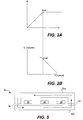
Referring to FIG. 5, a cross section of a core element 50 of the core array 40 according to the present invention is shown. Each of the core elements 50 includes a first core member 50 a positioned adjacent to and above the windings 38 and a second member 50 b positioned adjacent to and below the core windings 38. Together, the first core member 50 a and the second core member 50 b substantially form a loop around the core windings 38. A gap 54 is provided between the first and second members 50 a and 50 b. The gap allows a drop in the magnetic field between the two members 50 a and 50 b. In the particular embodiment shown, the core element 50 has a length that spans three windings 38. With this arrangement, each of the three windings 38 is magnetically coupled by the one core element 50. It should be understood, however, that this length is arbitrary and that the two members 50 a and 50 b of each core element 50 may be fabricated to span any number of windings 38.
Referring to FIG. 6A, a block diagram of the phase control circuit 46 of the present invention is shown. The phase control circuit 46 controls the phase of the plurality of pulsed input signals so that each is 360 degrees/N out of phase with respect to one another, where N equals the number of the regulator circuits 32. For example, if there are one hundred regulator circuits 32 (N=100), then the phase control circuit 46 controls the input signals 36 so that they are each 3.6 degrees out of phase with respect to one another. With this arrangement, any voltage ripple on the individual windings 38 tend to destructively interfere with one another, substantially cancelling each other out in the aggregate. As a result, a generally steady output voltage at the output node 42 is generated, which is the sum of the instantaneous voltage on each of the plurality of inductor windings respectively. Since the output signal at node 42 is relatively ripple-free and steady, the smoothing capacitor C2 can be either eliminated altogether or the size of the input capacitor C1 and, to some degree, the output capacitor C2 can be significantly reduced.
Referring to FIG. 6B, a diagram plotting the output voltage at the output node 42 over time is shown. The diagram illustrates a number of signals 58, each of which is representative of the voltage on the individual windings 38. As can be seen in the figure, the individual signals 58 are out of phase with respect to one another. As a result, the voltage ripple on the individual windings 38 tend to cancel each other out under low load conditions. Similarly the referred ripple to the input power supply are cancelled to a significant degree. The sum of the instantaneous voltage 58 on each of the plurality of inductor windings 38, however, is a relatively constant with the cancellation effect. The net result is a steady output signal or voltage 59 at the output node 42, represented by the thick black line in FIG. 6B.
Furthermore, with the arrangement the core elements 50 each spanning one or more windings 38, the magnetic coupling tends to average out or be substantially evenly shared or distributed across the core array 40. As a net result, the amount of magnetization “ripple” across the windings 38 is further minimized, resulting in a more steady output voltage signal at the node 42. Without this distributed coupling across the array 40, the individual core elements 50 would experience a greater level of magnetization ripple, leading to a higher level of hysteresis, radiative and eddy current related loss factors. As a result, the size of smoothing capacitor at the output node and input node 42 may be significantly reduced or eliminated all together.
The phase control circuit 46 also optionally includes a modulation circuit 56. The modulation circuit is configured to modulate the phase differences between the plurality of pulsed input signals 36 to either increase or decrease the transient current demands at the output node 42. Meeting high speed transient demand is often a challenge from a design perspective. By modulating the phase difference, typically for short periods of time, a transient surge in energy demand can be achieved. This phase modulation or short-term frequency modulation scheme thus enables spontaneous maximization of the energy transfer from the core to the output node.
Referring to FIGS. 7A-7H, a sequence of cross sections of a semiconductor substrate (e.g., a wafer) illustrating how the core elements 50 of the core array 40 are fabricated is shown.
In FIG. 7A, a seed layer 60 is formed over a substrate 62 in the location where the core elements 50 of the array 40 are to be formed. According to one embodiment, the seed layer 60 actually includes three layers of metal, for example, a Ti—Cu—Ti or Ti—FeNi—Ti, formed over the substrate surface by either sputtering or physical vapor deposition.
In the next step as illustrated in FIG. 7B, a blanket layer of molding material 64, such as photoresist or BCB, is applied over the seed layer 60.
The molding material 64 is then patterned using conventional lithography to form recess regions 66, as illustrated in FIG. 7C. Note the seed layer 60 is exposed at the bottom of the recess regions 66.
In the next step, the substrate is immersed in an electroplating bath. In the bath, the metal in the plating solution is plated onto the seed layer 60, forming the metal regions M as illustrated in FIG. 7D.
As illustrated in FIG. 7E, optionally, a nitride layer 68 is formed over the remaining molding material 64 and the metal M in the recess regions 66. A “lift off” gap 70 is provided under the nitride layers 68 on the molding material 64. In the next step, the molding material 64 is completely removed by exposure to a solvent through the lift off gaps 70.
As illustrated in FIG. 7F, a layer of low temperature oxide, nitride or a combination of the two is formed across the surface of the substrate 62, covering the top and side surfaces of the metal regions M.
As illustrated in FIG. 7G, a reactive ion anisotropic etch is then performed, which removes the oxide layer 72 and nitride layer 68 on the top surface of the metal regions M. The remaining oxide (or oxide/nitride) on the sidewalls of the metal regions M forms the spacers 52 described above. According to various embodiments, the thickness of the spacers may range from 500 Angstroms to 10 microns. The creation of the spacers 52 thus uses a novel processing scheme to electroplate the core elements in two stages on either side of the spacers, with the core elements sharing the electroplating seed layer.
In a final step as illustrated in FIG. 7H, the substrate undergoes a second plating bath, forming additional metal regions M, each separated by a spacer 52. The second metal regions M are thus self-aligned with the original metal regions M1 by the spacer 52.
The aforementioned process can be used to create the core elements 50 of the core array 40 as illustrated in FIGS. 4A through 4D. In other words, the process can be used to make core elements 50 of different or the same lengths and widths, in a uniform or staggered pattern, or of different metals (i.e., M1 and M2). In embodiments using two different metals, the core elements 50 of the first metal M1 are plated during the first electroplating operation and the core elements 50 of the second metal M2 are plated during the second plating operation. Similarly, the core members 50 a and 50 b can be formed using the same technique. After the lower members 50 b are fabricated on the substrate, the windings 38 are formed by a copper metallization step. Thereafter, the above process is again repeated to form the upper members 50 a. A dielectric layer is typically provided between the core members 50 a, 50 b and the winding 38 so that they are each electrically isolated from one another respectively. In various embodiments, the metals M1 and M2 may include a nickel-iron permalloy (80:20) or Orthonol (50:50); ZrCo, FeNiSi, FeNiCu, FeCo, CoMnZnFeNi, FeNiCo, or doped and non-doped combinations thereof.
While this invention has been described in terms of several preferred embodiments, there are alteration, permutations, and equivalents, which fall within the scope of this invention. It should also be noted that there are many alternative ways of implementing the methods and apparatuses of the present invention. For example, the steps of the present invention may be used to form a plurality of high value inductors 10 across many die on a semiconductor wafer. It is therefore intended that the following appended claims be interpreted as including all such alterations, permutations, and equivalents as fall within the true spirit and scope of the present invention.

Claims (23)

1. A method of forming an array of inductor core elements on a semiconductor substrate that includes integrated circuits, the method comprising:
forming a first set of spaced apart metallic core elements over the substrate;
forming isolation sidewalls on side surfaces of the core elements;
forming a second set of metallic core elements over the substrate after the formation of the isolation sidewalls, the first and second set of metallic core elements forming an inductor core element array, wherein:
the first and second sets of core elements are substantially co-planar and interleaved such that only the isolation sidewalls separate adjacent core elements;
the semiconductor substrate is a wafer having a multiplicity of dice formed thereon; and
a multiplicity of inductor core arrays are simultaneously formed on the wafer such that each die has an inductor core array formed thereon.
2. The method as recited in claim 1 wherein the forming of the isolation sidewalls includes:
depositing a conformal isolation layer over the substrate after the first set of core elements have been formed so that the isolation layer covers top and side surfaces of the first set of core elements and regions of the substrate between core elements in the first set of core elements; and
etching away portions of the isolation layer that cover the substrate in regions between core elements in the first set of core elements without removing the isolation sidewalls.
3. The method as recited in claim 2 wherein the etching also removes portions of the isolation layer that cover top surfaces of the first set of core elements.
4. The method as recited in claim 1 wherein the first set of core elements is formed by:
applying a metal seed layer over the substrate;
depositing a layer of photoresist over the metal seed layer;
patterning the photoresist using lithographic techniques to form recesses in the photoresist that expose portions of the metal seed layer; and
depositing a first metal material onto into the recesses to form the first set of core elements.
5. The method as recited in claim 4 wherein the applying of the metal seed layer over the substrate is performed prior to the formation of the first set of core elements and wherein the first metal material is deposited by electroplating.
6. The method as recited in claim 1 wherein different metal compositions are used to create the first and second sets of core elements such that the first and second sets of core elements have different magnetic coercivities.
7. The method as recited in claim 6 wherein the widths of core elements within at least one of the first and second sets of core elements vary.
8. The method as recited in claim 1 wherein the first and second sets of core elements are formed from the same materials.
9. The method as recited in claim 1 further comprising forming inductor windings arranged to interact with the inductor core element array.
10. The method as recited in claim 9, wherein the inductor windings are formed before the forming of the inductor core element array.
11. The method as recited in claim 1 wherein the thickness of the isolation sidewalls ranges from approximately 500 Angstroms to approximately 10 microns.
12. A method of forming an array of inductor core elements on a semiconductor substrate that includes integrated circuits, the method comprising:
forming a first set of spaced apart metallic core elements over the substrate;
forming isolation sidewalls on side surfaces of the core elements; and
forming a second set of metallic core elements over the substrate after the formation of the isolation sidewalls, wherein the first and second sets of core elements are substantially co-planar and interleaved such that only the isolation sidewalls separate adjacent core elements and wherein the first and second sets of core elements are formed from ferromagnetic materials wherein different metal compositions of the ferromagnetic materials are used to create the first and second sets of core elements such that the first and second sets of core elements have different magnetic coercivities.
13. The method as recited in claim 12 wherein:
the semiconductor substrate is a wafer having a multiplicity of dice formed thereon; and
a multiplicity of inductor core arrays are simultaneously formed on the wafer such that each die has an inductor core array formed thereon.
14. A method of forming an array of inductor core elements on a semiconductor substrate that includes integrated circuits, the method comprising:
forming a first set of spaced apart metallic core elements over the substrate;
forming isolation sidewalls on side surfaces of the core elements, wherein the forming of the isolation sidewalls includes:
depositing a conformal isolation layer over the substrate after the first set of core elements have been formed so that the isolation layer covers top and side surfaces of the first set of core elements and regions of the substrate between core elements in the first set of core elements; and
etching away portions of the isolation layer that cover the substrate in regions between core elements in the first set of core elements without removing the isolation sidewalls;
forming a second set of metallic core elements over the substrate after the formation of the isolation sidewalls, wherein the first and second sets of core elements are substantially co-planar and interleaved such that only the isolation sidewalls separate adjacent core elements;
after forming the first and second sets of metallic core elements, forming a set of one or more inductor core windings over the first and second sets of metallic core elements;
forming a third set of spaced apart inductor core elements over the set of inductor core windings;
forming isolation sidewalls on side surfaces of the third set of inductor core elements; and
forming a fourth set of metallic core elements over the inductor core windings, wherein the third and fourth sets of core elements are substantially coplanar and interleaved such that only isolation sidewalls separate adjacent core elements.
15. A method of forming an array of inductor core elements on a semiconductor substrate that includes integrated circuits, the method comprising:
forming a metal seed layer over the substrate;
depositing a layer of photoresist over the metal seed layer;
patterning the photoresist using lithographic techniques to form recesses in the photoresist that expose portions of the metal seed layer;
electroplating a first metal material into the recesses to form a first set of spaced apart core elements;
depositing a conformal isolation layer over the substrate after the first set of core elements have been formed so that the isolation layer covers top and side surfaces of the first set of core elements and regions of the substrate between core elements in the first set of core elements, thereby forming isolation sidewalls on each of the first set of core elements;
etching away portions of the isolation layer that cover the substrate in regions between core elements in the first set of core elements to expose portions of the metal seed layer without removing the isolation sidewalls; and
electroplating a second metal material after the isolation layer etching to form a second set of metallic core elements, wherein the first and second sets of core elements are substantially co-planar and interleaved such that only the isolation sidewalls separate adjacent core elements, wherein the first and second metal materials are ferromagnetic materials.
16. The method as recited in claim 15 wherein different metal compositions are used to create the first and second sets of core elements such that the first and second sets of core elements have different magnetic coercivities.
17. The method as recited in claim 15 wherein the first and second sets of core elements are formed from the same materials.
18. A method of forming an array of inductor core elements on a semiconductor substrate that includes integrated circuits, the method comprising:
forming a metal seed layer over the substrate;
depositing a layer of photoresist over the metal seed layer;
patterning the photoresist using lithographic techniques to form recesses in the photoresist that expose portions of the metal seed layer;
electroplating a first metal material into the recesses to form a first set of spaced apart core elements;
depositing a conformal isolation layer over the substrate after the first set of core elements have been formed so that the isolation layer covers top and side surfaces of the first set of core elements and regions of the substrate between core elements in the first set of core elements, thereby forming isolation sidewalls on each of the first set of core elements;
etching away portions of the isolation layer that cover the substrate in regions between core elements in the first set of core elements to expose portions of the metal seed layer without removing the isolation sidewalls;
electroplating a second metal material after the isolation layer etching to form a second set of metallic core elements, wherein the first and second sets of core elements are substantially co-planar and interleaved such that only the isolation sidewalls separate adjacent core elements; and
applying an insulating layer over the first set of core elements and the photoresist before the isolation sidewalls are formed, wherein portions of the insulating layer that cover the first set of core elements are left in place during the electroplating of the second metal material.
19. A method of forming an array of inductor core elements on a semiconductor substrate that includes integrated circuits, the method comprising:
forming a metal seed layer over the substrate;
depositing a layer of photoresist over the metal seed layer;
patterning the photoresist using lithographic techniques to form recesses in the photoresist that expose portions of the metal seed layer;
electroplating a first metal material into the recesses to form a first set of spaced apart core elements;
forming a nitride layer over the patterned photoresist and the first set of core elements, there being a gap under portions of the nitride layer that overlie the patterned photoresist;
removing the patterned photoresist at least in part by exposing the patterned photoresist to a solvent via the gap
depositing a conformal isolation layer over the substrate after the first set of core elements have been formed so that the isolation layer covers top and side surfaces of the first set of core elements and regions of the substrate between core elements in the first set of core elements, thereby forming isolation sidewalls on each of the first set of core elements;
etching away portions of the isolation layer that cover the substrate in regions between core elements in the first set of core elements to expose portions of the metal seed layer without removing the isolation sidewalls; and
electroplating a second metal material after the isolation layer etching to form a second set of metallic core elements, wherein the first and second sets of core elements are substantially co-planar and interleaved such that only the isolation sidewalls separate adjacent core elements.
20. A method of forming an array of inductor core elements on a substrate that includes, the method comprising:
forming a first set of spaced apart metallic core elements over the substrate;
forming isolation sidewalls on side surfaces of the core elements;
forming a second set of metallic core elements over the substrate after the formation of the isolation sidewalls, the first and second set of metallic core elements forming an inductor core element array, wherein:
at least one core element in the second set of core elements is positioned in a space between an associated adjacent pair of core elements in the first set of core elements;
the semiconductor substrate is a wafer having a multiplicity of dice formed thereon; and
a multiplicity of inductor core arrays are simultaneously formed on the wafer such that each die has an inductor core array formed thereon.
21. The method as recited in claim 20 wherein each core element in the second set of core elements that is positioned between an associated adjacent pair of first core elements substantially fills a gap between the associated adjacent pair of first core elements such that only the isolation sidewalls separate adjacent core elements from the first and second sets of core elements.
22. The method as recited in claim 20 wherein members of the first and second sets of core elements are substantially co-planar and interleaved such that only the isolation sidewalls separate adjacent core elements.
23. The method as recited in claim 20 wherein different metal compositions are used to create the first and second sets of core elements such that the first and second sets of core elements have different magnetic coercivities.
US12/250,385 2007-01-09 2008-10-13 Methods of forming inductors on integrated circuits Active 2028-03-07 US8042260B2 (en)

Priority Applications (1)

Application Number Priority Date Filing Date Title
US12/250,385 US8042260B2 (en) 2007-01-09 2008-10-13 Methods of forming inductors on integrated circuits

Applications Claiming Priority (2)

Application Number Priority Date Filing Date Title
US11/621,424 US7468899B1 (en) 2007-01-09 2007-01-09 Apparatus and method for wafer level fabrication of high value inductors on semiconductor integrated circuits
US12/250,385 US8042260B2 (en) 2007-01-09 2008-10-13 Methods of forming inductors on integrated circuits

Related Parent Applications (1)

Application Number Title Priority Date Filing Date
US11/621,424 Division US7468899B1 (en) 2007-01-09 2007-01-09 Apparatus and method for wafer level fabrication of high value inductors on semiconductor integrated circuits

Publications (2)

Publication Number Publication Date
US20090038142A1 US20090038142A1 (en) 2009-02-12
US8042260B2 true US8042260B2 (en) 2011-10-25

Family

ID=40134256

Family Applications (3)

Application Number Title Priority Date Filing Date
US11/621,424 Active US7468899B1 (en) 2007-01-09 2007-01-09 Apparatus and method for wafer level fabrication of high value inductors on semiconductor integrated circuits
US12/250,385 Active 2028-03-07 US8042260B2 (en) 2007-01-09 2008-10-13 Methods of forming inductors on integrated circuits
US12/250,382 Active US7755463B2 (en) 2007-01-09 2008-10-13 Integrated circuits with inductors

Family Applications Before (1)

Application Number Title Priority Date Filing Date
US11/621,424 Active US7468899B1 (en) 2007-01-09 2007-01-09 Apparatus and method for wafer level fabrication of high value inductors on semiconductor integrated circuits

Family Applications After (1)

Application Number Title Priority Date Filing Date
US12/250,382 Active US7755463B2 (en) 2007-01-09 2008-10-13 Integrated circuits with inductors

Country Status (1)

Country Link
US (3) US7468899B1 (en)

Cited By (3)

* Cited by examiner, † Cited by third party
Publication number Priority date Publication date Assignee Title
US8314676B1 (en) * 2011-05-02 2012-11-20 National Semiconductor Corporation Method of making a controlled seam laminated magnetic core for high frequency on-chip power inductors
US20140347025A1 (en) * 2013-05-21 2014-11-27 Taiwan Semiconductor Manufacturing Co. Ltd. Integrated Voltage Regulator Substrate System and Methods Having a Coupled-Magnetic-Core Inductor
US11393776B2 (en) * 2018-05-17 2022-07-19 Advanced Semiconductor Engineering, Inc. Semiconductor device package and method of manufacturing the same

Families Citing this family (20)

* Cited by examiner, † Cited by third party
Publication number Priority date Publication date Assignee Title
US8299885B2 (en) 2002-12-13 2012-10-30 Volterra Semiconductor Corporation Method for making magnetic components with M-phase coupling, and related inductor structures
US9013259B2 (en) 2010-05-24 2015-04-21 Volterra Semiconductor Corporation Powder core material coupled inductors and associated methods
US8952776B2 (en) 2002-12-13 2015-02-10 Volterra Semiconductor Corporation Powder core material coupled inductors and associated methods
US20080067990A1 (en) * 2006-09-19 2008-03-20 Intersil Americas Inc. Coupled-inductor assembly with partial winding
US8963521B2 (en) 2007-06-08 2015-02-24 Intersil Americas LLC Power supply with a magnetically uncoupled phase and an odd number of magnetically coupled phases, and control for a power supply with magnetically coupled and magnetically uncoupled phases
US8179116B2 (en) * 2007-06-08 2012-05-15 Intersil Americas LLC Inductor assembly having a core with magnetically isolated forms
US8704500B2 (en) * 2007-08-14 2014-04-22 Intersil Americas LLC Sensing a phase-path current in a multiphase power supply such as a coupled-inductor power supply
US8320136B2 (en) * 2007-08-31 2012-11-27 Intersil Americas Inc. Stackable electronic component
US7898236B2 (en) 2008-04-10 2011-03-01 Intersil Americas Inc. Varying operation of a voltage regulator, and components thereof, based upon load conditions
US8004303B2 (en) * 2008-12-08 2011-08-23 National Semiconductor Corporation Method and system for measuring film stress in a wafer film
US8299882B2 (en) 2009-07-22 2012-10-30 Volterra Semiconductor Corporation Low profile inductors for high density circuit boards
US8410576B2 (en) 2010-06-16 2013-04-02 National Semiconductor Corporation Inductive structure and method of forming the inductive structure with an attached core structure
US8102236B1 (en) 2010-12-14 2012-01-24 International Business Machines Corporation Thin film inductor with integrated gaps
US8716991B1 (en) 2011-02-28 2014-05-06 Volterra Semiconductor Corporation Switching power converters including air core coupled inductors
US20130114829A1 (en) * 2011-11-04 2013-05-09 James J. McGourty, JR. Recursive audio modulation system using nested inductor arrays
US10128035B2 (en) 2011-11-22 2018-11-13 Volterra Semiconductor LLC Coupled inductor arrays and associated methods
US9373438B1 (en) 2011-11-22 2016-06-21 Volterra Semiconductor LLC Coupled inductor arrays and associated methods
US9083332B2 (en) 2012-12-05 2015-07-14 Volterra Semiconductor Corporation Integrated circuits including magnetic devices
EP2858224A1 (en) * 2013-10-07 2015-04-08 Dialog Semiconductor GmbH Assymetric inductor in multi-phase DCDC converters
WO2018057227A1 (en) * 2016-09-22 2018-03-29 Apple Inc. Coupled inductor structures utilizing magnetic films

Citations (14)

* Cited by examiner, † Cited by third party
Publication number Priority date Publication date Assignee Title
US5204809A (en) 1992-04-03 1993-04-20 International Business Machines Corporation H-driver DC-to-DC converter utilizing mutual inductance
US5869148A (en) 1991-04-23 1999-02-09 Webcraft Technologies Inc. Process for the in-line, high speed manufacturing of magnetic products
US20020097129A1 (en) 2000-02-16 2002-07-25 Johnson F. Scott Method of fabricating a miniaturized integrated circuit inductor and transformer fabrication
US6466401B1 (en) * 1999-06-02 2002-10-15 Read-Rite Corporation Thin film write head with interlaced coil winding and method of fabrication
US20040123449A1 (en) * 2001-05-21 2004-07-01 Teruo Inaguma Thin-film coil, magnetic head, method of manufacturing the thin-film coil, and method of manufacturing the magnetic head
US6867903B2 (en) 2000-03-21 2005-03-15 Nippon Telegraph And Telephone Corporation Optical parametric circuit
US6943535B1 (en) 2002-10-17 2005-09-13 Analog Devices, Inc. Multiple-phase DC-DC converter topology
US7002325B2 (en) 2003-10-20 2006-02-21 Intersil Americas Inc. Clocked cascading current-mode regulator with high noise immunity and arbitrary phase count
US7012414B1 (en) 2004-08-19 2006-03-14 Coldwatt, Inc. Vertically packaged switched-mode power converter
US7061359B2 (en) 2003-06-30 2006-06-13 International Business Machines Corporation On-chip inductor with magnetic core
US7176662B2 (en) 2005-02-23 2007-02-13 Coldwatt, Inc. Power converter employing a tapped inductor and integrated magnetics and method of operating the same
US7268410B1 (en) 2005-01-24 2007-09-11 National Semiconductor Corporation Integrated switching voltage regulator using copper process technology
US7292128B2 (en) 2002-12-19 2007-11-06 Cooper Technologies Company Gapped core structure for magnetic components
US7319572B2 (en) * 2003-05-29 2008-01-15 Tdk Corporation Thin film coil and method of forming the same, and thin film magnetic head and method of manufacturing the same

Family Cites Families (7)

* Cited by examiner, † Cited by third party
Publication number Priority date Publication date Assignee Title
US3290633A (en) * 1961-12-14 1966-12-06 Hitachi Ltd Laminated core with bidirectional joints
US3395373A (en) * 1966-08-31 1968-07-30 Westinghouse Electric Corp Three-phase transformer having four core legs
GB8818849D0 (en) * 1988-08-09 1988-09-14 Emi Plc Thorn Electromagnetic identification system
US7352269B2 (en) * 2002-12-13 2008-04-01 Volterra Semiconductor Corporation Method for making magnetic components with N-phase coupling, and related inductor structures
WO2005055256A1 (en) * 2003-12-02 2005-06-16 Adelaide Research & Innovation Pty Ltd Method of forming and testing the formation of amorphous metal objects
US7463131B1 (en) * 2005-01-24 2008-12-09 National Semiconductor Corporation Patterned magnetic layer on-chip inductor
US7342477B2 (en) * 2005-07-01 2008-03-11 The Boeing Company Inductor

Patent Citations (14)

* Cited by examiner, † Cited by third party
Publication number Priority date Publication date Assignee Title
US5869148A (en) 1991-04-23 1999-02-09 Webcraft Technologies Inc. Process for the in-line, high speed manufacturing of magnetic products
US5204809A (en) 1992-04-03 1993-04-20 International Business Machines Corporation H-driver DC-to-DC converter utilizing mutual inductance
US6466401B1 (en) * 1999-06-02 2002-10-15 Read-Rite Corporation Thin film write head with interlaced coil winding and method of fabrication
US20020097129A1 (en) 2000-02-16 2002-07-25 Johnson F. Scott Method of fabricating a miniaturized integrated circuit inductor and transformer fabrication
US6867903B2 (en) 2000-03-21 2005-03-15 Nippon Telegraph And Telephone Corporation Optical parametric circuit
US20040123449A1 (en) * 2001-05-21 2004-07-01 Teruo Inaguma Thin-film coil, magnetic head, method of manufacturing the thin-film coil, and method of manufacturing the magnetic head
US6943535B1 (en) 2002-10-17 2005-09-13 Analog Devices, Inc. Multiple-phase DC-DC converter topology
US7292128B2 (en) 2002-12-19 2007-11-06 Cooper Technologies Company Gapped core structure for magnetic components
US7319572B2 (en) * 2003-05-29 2008-01-15 Tdk Corporation Thin film coil and method of forming the same, and thin film magnetic head and method of manufacturing the same
US7061359B2 (en) 2003-06-30 2006-06-13 International Business Machines Corporation On-chip inductor with magnetic core
US7002325B2 (en) 2003-10-20 2006-02-21 Intersil Americas Inc. Clocked cascading current-mode regulator with high noise immunity and arbitrary phase count
US7012414B1 (en) 2004-08-19 2006-03-14 Coldwatt, Inc. Vertically packaged switched-mode power converter
US7268410B1 (en) 2005-01-24 2007-09-11 National Semiconductor Corporation Integrated switching voltage regulator using copper process technology
US7176662B2 (en) 2005-02-23 2007-02-13 Coldwatt, Inc. Power converter employing a tapped inductor and integrated magnetics and method of operating the same

Non-Patent Citations (7)

* Cited by examiner, † Cited by third party
Title
"The Concise Colour Science Dictionary", Oxford University Press, 1997, p. 708.
U.S. Appl. No. 10/658,433, filed Sep. 8, 2003.
U.S. Appl. No. 11/111,660, filed Apr. 21, 2005.
U.S. Appl. No. 11/137,767, filed May 25, 2005.
U.S. Appl. No. 11/274,932, filed Nov. 14, 2005.
U.S. Appl. No. 11/495,143, filed Jul. 27, 2006.
U.S. Appl. No. 11/504,972, filed Aug. 15, 2006.

Cited By (5)

* Cited by examiner, † Cited by third party
Publication number Priority date Publication date Assignee Title
US8314676B1 (en) * 2011-05-02 2012-11-20 National Semiconductor Corporation Method of making a controlled seam laminated magnetic core for high frequency on-chip power inductors
US20140347025A1 (en) * 2013-05-21 2014-11-27 Taiwan Semiconductor Manufacturing Co. Ltd. Integrated Voltage Regulator Substrate System and Methods Having a Coupled-Magnetic-Core Inductor
US9748324B2 (en) * 2013-05-21 2017-08-29 Taiwan Semiconductor Manufacturing Co., Ltd. Method of fabricating magnetic core inductors for an integrated voltage regulator
US10297657B2 (en) 2013-05-21 2019-05-21 Taiwan Semiconductor Manufacturing Co., Ltd. Magnetic core inductors for integrated voltage regulator
US11393776B2 (en) * 2018-05-17 2022-07-19 Advanced Semiconductor Engineering, Inc. Semiconductor device package and method of manufacturing the same

Also Published As

Publication number Publication date
US7468899B1 (en) 2008-12-23
US20090038142A1 (en) 2009-02-12
US7755463B2 (en) 2010-07-13
US20090040000A1 (en) 2009-02-12

Similar Documents

Publication Publication Date Title
US8042260B2 (en) Methods of forming inductors on integrated circuits
US9679958B2 (en) Methods for manufacturing integrated multi-layer magnetic films
US7250842B1 (en) MEMS inductor with very low resistance
US10431371B2 (en) Manufacturing methods for magnetic core inductors with biased permeability
US8407883B2 (en) Magnetically enhanced power inductor with self-aligned hard axis magnetic core produced in an applied magnetic field using a damascene process sequence
US9337251B2 (en) Integrated magnetic core inductors with interleaved windings
Lee et al. Fabrication and analysis of high-performance integrated solenoid inductor with magnetic core
US7875955B1 (en) On-chip power inductor
US7897472B2 (en) Apparatus and method for wafer level fabrication of high value inductors on semiconductor integrated circuits
US10347709B2 (en) Methods of manufacturing integrated magnetic core inductors with vertical laminations
US11404197B2 (en) Via for magnetic core of inductive component
US7423509B2 (en) Coil comprising several coil branches and micro-inductor comprising one of the coils
US20110025443A1 (en) Apparatus and method for wafer level fabrication of high value inductors on semiconductor integrated circuits
US20230326654A1 (en) Magnetic core with vertical laminations having high aspect ratio
WO1997042662A1 (en) Integrable circuit inductor
US10629357B2 (en) Apparatus and methods for magnetic core inductors with biased permeability
US20090160592A1 (en) Helical core on-chip power inductor
US11302469B2 (en) Method for fabricating inductors with deposition-induced magnetically-anisotropic cores
US20080106364A1 (en) Spiral-shaped closed magnetic core and integrated micro-inductor comprising one such closed magnetic core
US20100194510A1 (en) Inductive Electrical Device
US10210986B2 (en) Integrated magnetic core inductor with vertical laminations
Sato et al. FeCoBN magnetic thin film inductor for MHz switching micro DC-DC converters
Park et al. Micromachined inductors with electroplated magnetically anisotropic alloy cores

Legal Events

Date Code Title Description
AS Assignment

Owner name: NATIONAL SEMICONDUCTOR CORPORATION, CALIFORNIA

Free format text: ASSIGNMENT OF ASSIGNORS INTEREST;ASSIGNORS:HOPPER, PETER J.;JOHNSON, PETER;SMEYS, PETER;AND OTHERS;REEL/FRAME:021724/0151;SIGNING DATES FROM 20080917 TO 20080918

Owner name: NATIONAL SEMICONDUCTOR CORPORATION, CALIFORNIA

Free format text: ASSIGNMENT OF ASSIGNORS INTEREST;ASSIGNORS:HOPPER, PETER J.;JOHNSON, PETER;SMEYS, PETER;AND OTHERS;SIGNING DATES FROM 20080917 TO 20080918;REEL/FRAME:021724/0151

STCF Information on status: patent grant

Free format text: PATENTED CASE

FPAY Fee payment

Year of fee payment: 4

MAFP Maintenance fee payment

Free format text: PAYMENT OF MAINTENANCE FEE, 8TH YEAR, LARGE ENTITY (ORIGINAL EVENT CODE: M1552); ENTITY STATUS OF PATENT OWNER: LARGE ENTITY

Year of fee payment: 8

MAFP Maintenance fee payment

Free format text: PAYMENT OF MAINTENANCE FEE, 12TH YEAR, LARGE ENTITY (ORIGINAL EVENT CODE: M1553); ENTITY STATUS OF PATENT OWNER: LARGE ENTITY

Year of fee payment: 12