US8046532B2 - Content-addressable memories and state machines for performing three-byte matches and secondary matches, and for providing error protection - Google Patents
Content-addressable memories and state machines for performing three-byte matches and secondary matches, and for providing error protection Download PDFInfo
- Publication number
- US8046532B2 US8046532B2 US12/195,319 US19531908A US8046532B2 US 8046532 B2 US8046532 B2 US 8046532B2 US 19531908 A US19531908 A US 19531908A US 8046532 B2 US8046532 B2 US 8046532B2
- Authority
- US
- United States
- Prior art keywords
- match
- state
- primary
- string
- byte
- Prior art date
- Legal status (The legal status is an assumption and is not a legal conclusion. Google has not performed a legal analysis and makes no representation as to the accuracy of the status listed.)
- Active, expires
Links
Images


Classifications
-
- G—PHYSICS
- G11—INFORMATION STORAGE
- G11C—STATIC STORES
- G11C15/00—Digital stores in which information comprising one or more characteristic parts is written into the store and in which information is read-out by searching for one or more of these characteristic parts, i.e. associative or content-addressed stores
Definitions
- the invention is directed towards a method and system for detecting matching strings in a string of characters.
- the method comprises detecting at least one match of sequential input characters with sequential characters stored in memory locations of a content addressable memory (CAM).
- CAM content addressable memory
- the method includes tracking at least one potential string match in progress, wherein a potential string match is two to N ⁇ 1 sequential input characters matching with two to N ⁇ 1 sequential characters stored in the memory locations of the CAM.
- the method includes tracking the length of the at least one potential string match.
- the method includes tracking the length of at least one primary match and at least one secondary match, wherein the at least one primary match and the at least one secondary match are matches of N or more sequential characters.
- the method includes allowing each of at least one potential string match to transition to a secondary match if the at least one potential string match can transition from N ⁇ 1 to N character matches on the next input character after a primary match has begun; terminating a primary match when the next sequential character stored in the CAM does not match a current input character.
- the method includes terminating a secondary match when the next sequential character stored in the CAM does not match the current input character.
- the method includes determining the longest string match of a primary match or a secondary match.
- the method includes outputting the address of the determined longest match when the at least one primary match and the at least one secondary match have terminated.
- the method includes resetting the at least one potential string match after a delay of one input character following the beginning of the at least one primary match, wherein potential string matches are not allowed to begin until the at least one primary match is terminated by a non-matching input character.
- the method includes resetting the at least one potential string match after a delay of one input character following the termination of all primary matches and the continuation of the at least one secondary match, wherein the at least one potential string match is not allowed to begin until all secondary matches have terminated.
- the method includes tracking the plurality of potential string matches comprises selecting a longest primary match when the longest primary match is longer than the longest secondary match.
- the method includes tracking the plurality of potential string matches comprises selecting the longest primary match when the longest primary match is the same length as the longest secondary match.
- the method includes tracking the plurality of potential string matches comprises selecting the longest secondary match when the longest secondary match is longer than the longest primary match.
- the method includes stopping at an arbitrary primary match length or at an arbitrary secondary match length, regardless of whether the at least one primary match or the at least one secondary match continues.
- the method includes outputting the address of the match closest to the last written character in the case of two or more primary matches terminating simultaneously.
- the method includes outputting the address of the match closest to the last written character in the case of two or more secondary matches terminating simultaneously.
- the method is pipelined.
- the method includes outputting the address of the longest at least one primary match when the at least one primary match has terminated, independent of any secondary matches.
- the method includes outputting the address of the longest at least one secondary match when the at least one secondary match has terminated, independent of any primary matches.
- the method includes storing at least the string of characters in a content addressable memory, wherein an individual memory cell in the content addressable memory stores a character of the string of characters.
- the method includes comparing input data to the characters stored in the individual memory cells to determine if the input data matches the character stored in the individual memory cell.
- the method includes defining a plurality of discrete states in a plurality of state machines, the plurality of discrete states comprising at least a write state, a one-byte match state, a two-byte match state, a three-byte match state, a secondary match state, and a secondary match delay state.
- the method includes transitioning between states in a plurality of concurrently operating state machines based on the present state of the state machine and the presence of a running match.
- the transitioning includes entering the write state in each individual state machine in response to a character being stored in an individual memory cell.
- the transitioning includes entering the one-byte match state in each individual state machine when starting in the write state and when there is a one-byte match between the input data and a first character of the primary matching string stored in a first memory cell.
- the transitioning includes entering the two-byte match state in each individual state machine when starting in the one-byte match state and when there is a second match between the input data and a second character of the primary matching string stored in a second memory cell.
- the transitioning includes entering the three-byte match state in each individual state machine when starting in the two-byte match state, when there is a third match between the input data and a third character of the primary matching string stored in the third memory cell, and when no state machine is outputting a primary match signal.
- the transitioning includes entering the secondary match state instead of the three-byte match state when a state machine is outputting the primary match signal and when there is a third match between the input data and a third character of a secondary matching string stored in a fourth memory cell, wherein the state machines detect the secondary matching string concurrently while detecting the primary matching string.
- the method includes outputting a primary match signal that indicates a three-byte match when the state machine is in the three-byte match state.
- the method includes outputting signals representing sequences of matched characters.
- the method includes detecting a longer match of the first and secondary matches and selecting the longer matched character string of the two match character strings when the shorter match ends.
- the secondary match is a match which starts with a different input byte than the primary matching string.
- the method includes outputting an input character as an uncompressed literal before matching to improve the compression ratio.
- the transitioning includes entering the secondary match delay state when a state machine detects a match between the input data and a character stored in an associated memory cell, when a secondary match is ongoing, and when a separate state machine is not outputting a primary match signal.
- the storing includes storing at least one error correction bit corresponding to the string of characters and analyzing the at least one error correction bit to determine whether any error affects the stored characters.
- the method is used for routing packets under the Internet Protocol.
- the at least one error correction bit includes one or more bits that implements a Hamming encoding scheme.
- the at least one error correction bit comprises one or more parity bits.
- the at least one error correction bit comprises one or more error correction bits that are generated internally and locally at the memory cell based on the stored characters.
- the at least one error correction bit comprises one or more error correction bits that are generated externally to the memory cell and are received along with data that is stored in the memory cell.
- the at least one error correction bit enables detection of hard or soft error and reduces the occurrence of false matches.
- the system includes a string match module and an output module.
- the string match module comprises a content addressable memory, wherein the content addressable memory comprises a plurality of individual memory cells, a plurality of compare circuits, and a plurality of individual state machines, each individual state machine operating concurrently.
- each individual memory cell is logically connected to an individual compare circuit.
- the plurality of individual memory cells stores at least a string of characters.
- each individual memory cell stores a character of the string of characters.
- each individual compare circuit is logically connected to an individual state machine.
- each individual state machine is associated with an individual memory cell and with an individual compare circuit.
- each individual compare circuit outputs to the associated state machines an intermediate match signal that indicates whether the input data matches the character stored in the associated memory cell.
- each of the plurality of individual state machines comprises a plurality of discrete states, the plurality of discrete states comprising at least a write state, a one-byte match state, a two-byte match state, a three-byte match state, a secondary match state, and a secondary match delay state.
- each individual state machine enters the write state in response to a character being stored in the memory cell associated with the individual state machine.
- each individual state machine enters the one-byte match state when starting in the write state and when there is a one-byte match between the input data and a first character of a primary matching string stored in a first memory cell.
- each individual state machine enters the two-byte match state when starting in the one-byte match state and when there is a second match between the input data and a second character of the primary matching string stored in a second memory cell.
- each individual state machine enters the three-byte match state when starting in the two-byte match state, when there is a third match between the input data and a third character of the primary matching string stored in a third memory cell, and when no state machine is outputting a primary match signal.
- each individual state machine outputs a primary match signal that indicates a three-byte match of the primary matching string when the state machine is in the three-byte match state and there is not a primary match signal being output.
- a state machine when each individual state machine is in the two-byte match state and when the primary match signal is being output, thereby signifying a three-byte match for the primary matching string, a state machine enters the secondary match state instead of the three-byte match state when there is a third match between the input data and a third character of a secondary matching string stored in a fourth memory cell, wherein the state machines detects the secondary matching string concurrently while detecting the primary matching string.
- the output module outputs sequences of matched data.
- the plurality of state machines detects a longer match of the primary matching string and the secondary matching string and selects the longer matched character string.
- the secondary matching string is a match which starts with a different input byte than the primary matching string.
- a character in an input character string may be output as an uncompressed literal before matching to improve the compression ratio.
- the state machine enters the secondary match delay state when there is an intermediate match, a secondary match is ongoing, and a separate state machine is not outputting a primary match signal.
- the individual memory cells further stores at least one error correction bit that corresponds to the string of characters, and wherein the system further comprises an error detection circuit that analyzes the at least one error correction bit to determine whether any error affects the stored characters.
- system is used for routing packets under the Internet Protocol.
- the at least one error correction bit includes one or more bits that implements a Hamming encoding scheme.
- the at least one error correction bit comprises one or more parity bits.
- the at least one error correction bit comprises one or more error correction bits that are generated internally and locally at the memory cell based on the stored characters.
- the at least one error correction bit comprises one or more error correction bits that are generated externally to the memory cell and are received along with data that is stored in the memory cell.
- the at least one error correction bit enables detection of hard or soft error and reduces the occurrence of false matches.
- FIG. 1 is a block diagram of systems or environments in which content-addressable memories (CAMs) and state machines for performing three-byte matches may operate, illustrating implementations in which data is shifted between the CAMs.
- CAMs content-addressable memories
- FIG. 2 is a block diagram of systems or environments in which content-addressable memories (CAMs) and state machines for performing three-byte matches may operate, illustrating implementations in which state information is shifted between state machines associated with the CAMs.
- CAMs content-addressable memories
- FIG. 3 is a combined block and flow diagram of signal transfers between CAM cells, compare circuits, and state machines that are shown in FIGS. 1 and 2 .
- FIG. 4 is a combined block and flow diagram of components and signal flows related to implementations in which CAM cells shift data from one to another, while maintaining state information within individual CAM cells.
- FIG. 5 is a combined block and flow diagram of components and signal flows related to passing state information between different state machines associated with different CAM cells.
- FIG. 6 is a state diagram of example states and transitions of the state machines shown in FIGS. 1-5 .
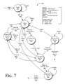
- FIG. 7 is a state diagram of example states and transitions suitable for tracking runs of byte matches occurring in a CAM including “Secondary Matches”. Secondary matches are matches which start with a different input byte than the initial runs of byte matches. The initial runs of byte matches are referred to herein as “Global Matches”.
- FIG. 8 is a state diagram of extensions of the state machines for providing a two-byte match capability.
- FIG. 9 is a block diagram of components and signal flows that provide error detection schemes for reducing the risk of false matches occurring in the CAM cells.
- tools systems, methods, and computer-readable storage media (collectively, “tools”) that are capable of performing and/or supporting many techniques and processes.
- the following discussion describes exemplary ways in which the tools provide content-addressable memories and state machines for performing three-byte matches. This discussion also describes other techniques and/or processes that may be performed by the tools.
- FIG. 1 illustrates systems or environments 100 in which the content-addressable memories (CAMs) and state machines for performing three-byte matches may operate.
- the operating environment 100 may include a compressor component 102 that is operative to receive as input a stream of raw or uncompressed input data 104 , and to produce as output a set of compressed symbols 106 .
- the input data 104 may be organized, for example, by bytes.
- the compressor 102 may implement, for example, the DEFLATE compression algorithm, as defined by RFC 1951, which is incorporated by reference as if set forth verbatim herein.
- the compressor may include a string match module 108 that is operative to receive as input at least part of a data bus 110 , and to generate signals that represent strings of current input data (e.g., bytes) that match previously input date (e.g., bytes).
- the data bus may present a sequence of input data, with FIG. 1 representing the input data at 112 .
- FIG. 1 also denotes the output of the string match module at 114 .
- the compressor may also include an encoding module that is operative to receive signals representing the sequences of matching data 114 , and to encode the matching data 114 into corresponding encoded symbols 118 . Taken as a whole, the encoded symbols 118 may form the compressed symbols 106 .
- the string match module 108 may include one or more CAMs, with FIG. 1 providing an example CAM at 120 .
- the CAM 120 may include a plurality of individually-addressable storage or memory cells, with FIG. 1 illustrating three examples of such cells, denoted at 122 a , 122 b , and 122 n (collectively, memory cells 122 ). As the data bus 110 presents new input data, the new data may be loaded into the memory cells 122 . While FIG. 1 illustrates a CAM having three memory cells, the CAM 120 may be of any convenient size or storage capacity, and thus may contain any number of memory cells.
- this new input data may be written sequentially to different memory cells.
- FIG. 2 provides examples of these implementations.
- the new input data is written to one memory cell, and previously-written data is shifted to other memory cells.
- FIG. 1 provides examples of the latter implementations, with new input data written to, for example, the memory cell 122 a .
- the memory cell 122 a may shift its previous contents to the next memory cell 122 b , as represented by the arrow 123 a .
- the memory cell 122 b may shift its previous contents to the next memory cell 122 n , and so on. in the example shown in FIG. 1 , the memory cell 122 n would not shift its data back around to the memory cell 122 a.
- the complete block of raw data bytes may be associated with a set of compressed symbols 106 .
- the compressed symbols may be stored or otherwise persisted for later access, may be transmitted to a recipient over a network, or otherwise disposed.
- the string match module 108 may also include a plurality of compare circuits, with FIG. 1 providing three examples of the compare circuits at 124 a , 124 b , and 124 n (collectively, compare circuits 124 ) that are associated respectively with the memory cells 122 a , 122 b , and 122 n . While FIG. 1 illustrates three compare circuits 124 , it is noted that the number of compare circuits 124 included in a given implementation may vary, depending on the number of memory cells 122 .
- the compare circuits may be implemented, for example, using suitable combinatorial logic, the details of which are omitted from the Figures herein to promote clarity. Additionally, the Figures show the compare circuits 124 separately from the memory cells 122 only for ease of reference and description, but not to limit possible implementations. More specifically, the memory cells 122 and the compare circuits 124 may be implemented together or separately in different applications.
- the string match module 108 may also include respective instances of state machines that are associated with the memory cells and the compare circuits.
- FIG. 1 provides three examples of the state machines, denoted at 126 a , 126 b , and 126 n (collectively, 126 ).
- the blocks 126 a - 126 n may represent circuitry used to realize the state machines, while FIGS. 6-8 below provide examples of the individual states and transitions that the state machines may include.
- Individual instances of the state machines are associated with individual memory cells and with individual compare circuits, as shown by the arrows connecting these items in FIG. 1 .
- the compare circuits 124 may compare the present contents of their corresponding memory cells with the input byte 112 that is currently asserted on the data bus 110 .
- the compare circuits may generate output signals that indicate whether the present contents of the corresponding memory cells match the input byte asserted on the address bus.
- FIG. 1 represents these match signals by the arrows 125 a , 125 b , and 125 n , which connect the respective compare circuits 124 a , 124 b , and 124 n with the corresponding state machines 126 a , 126 b , and 126 n .
- state is maintained within the given machines 126 , and the machines 126 do not share or shift state between themselves.
- FIG. 2 provides examples in which the machines 126 may pass state to one another.
- the state machines 126 may transition states in response to the match signals 125 generated by the compare circuits. In turn, the state machines may output match signals 128 that indicate whether a match of some predetermined minimum byte length (e.g., three bytes) has occurred within the CAM 120 . As described in more detail below, one or more of the memory cells and/or related state machines may assert the match signal 128 to notify the other CAM cells and/or related state machines that the match has occurred.
- some predetermined minimum byte length e.g., three bytes
- FIG. 2 illustrates arrangements 200 in which CAMs and state machines for performing three-byte matches may operate, illustrating implementations in which state information is shifted between state machines associated with the CAMs.
- FIG. 2 illustrates arrangements 200 in which CAMs and state machines for performing three-byte matches may operate, illustrating implementations in which state information is shifted between state machines associated with the CAMs.
- FIG. 2 illustrates examples in which the state machines pass state information from one to another, in response to the match signals 125 .
- FIG. 2 denotes this shifted state information generally at 202 , with the state machine 126 a shifting state information 202 a to the state machine 126 b , and the state machine 126 b shifting state information 202 b to the state machine 126 n .
- the state machine 126 n may also shift state information 202 n back to the state machine 126 a , unless this state information represents a reset state.
- a given state machine associated with a given memory cell may receive state information from another state machine associated with a previously-addressable memory cell.
- FIG. 3 illustrates data and signal flows 300 between the memory cells, compare circuits, and state machines.
- FIG. 3 illustrates data and signal flows 300 between the memory cells, compare circuits, and state machines.
- input data 112 is being written to a given memory cell 122 a .
- all input data may be written to one memory cell 122 a as the data arrives, with previously-stored data being shifted sequentially to the memory cells 122 b , 122 n , and so on.
- different instances of the input data may be written to different memory cells, in sequence as the input data arrives, as indicated by the dashed lines 112 b and 112 n.
- the different memory cells 122 may be controlled by respective write-enable signals, with FIG. 3 showing three examples of write enable signals at 302 a , 302 b , and 302 n (collectively, write enable signals 302 ).
- the write-enable signals 302 may be the outputs of suitable logic (not shown) for decoding at least part of an address bus.
- the write-enable signals are operative to strobe input data (e.g., one or more bytes) into one of the memory cells when the write-enable signals assume some signal level.
- the write-enable signals may be defined as active-high signals.
- the write-enable signal 302 a for the memory cell 122 a becomes active, causing the memory cell 122 a to latch the input data 112 that is currently asserted on the data bus.
- the write-enable signal 302 b for the memory cell 122 b would become active, and the write-enable signal 302 a would be de-asserted.
- FIG. 3 denotes the respective memory cell contents at 304 a , 304 b , and 304 n .
- signals representing the input data 112 may be routed to the compare circuits 124 , as represented by the lines 306 a , 306 b , and 306 n.
- the various compare circuits may then compare the input data to the contents of the memory cells, and may generate match signals that indicate the results of these comparisons.
- FIG. 3 provides three examples of these match signals, carried forward at 125 a , 125 b , and 125 n (collectively, match signals 125 ).
- These match signals 125 may represent character match signals. More specifically, the match signal 125 a indicates whether the contents of the memory cell 122 a match the input data 112 , the match signal 125 b indicates whether the contents of the memory cell 122 b match the input data 112 , and the match signal 125 n indicates whether the contents of the memory cell 122 n match the input data 112 .
- zero or more of the compare circuits may assert active or positive signals, indicating matches or non-matches between the corresponding memory cells and the input data.
- the state machines 126 may receive as input at least the match signals 125 .
- the state machines 126 may transition states in response to at least the match signals 125 .
- the state machine 126 a receives the match signal 125 a as input
- the state machine 126 b receives the match signal 125 b as input
- the state machine 126 n receives the match signal 125 n as input.
- the state machines 126 may provide output signals that indicate some level of match between an ongoing sequence of input bytes 112 and the contents of consecutive memory cells 122 . More specifically, FIG. 3 provides examples of three output match signals, denoted at 312 a , 312 b , and 312 n (collectively, output match signals 312 ). In an example implementation in which the systems 100 are detecting matches of three bytes or more, the output signal from a given state machine may indicate whether that state machine has detected the third byte in such an ongoing match, thereby indicating the existence of a three-byte match between the input data 112 and data already stored in the memory cells 122 .
- the description herein refers to an ongoing match between the input bytes and the memory cells of at least some predefined byte length as a “global” match. Assuming a three-byte threshold length, an ongoing match of three bytes or more may be considered a “global” match, and the output signals 312 may reflect the presence or absence of such an ongoing global match. For example, if the state machine 126 n detects the third byte of an ongoing match in its memory cell 122 n , the state machine 126 n may activate its output signal 312 n to advise the other state machines 126 a and 126 b that a global match is ongoing.
- FIG. 3 represents the output match signals 312 as double-headed arrows. Taken as a whole, the output match signals 312 may define the state of the match signal 128 .
- the tools described herein may provide implementations in which data is shifted from one memory cell (e.g., 122 ) to another as new data arrives.
- state information does not pass from one state machine (e.g., 126 ) to another.
- FIG. 4 states are described further in FIG. 4 below.
- input data it is written to different memory cells in sequence, and state information is passed from one state machine to another.
- FIG. 5 states are described further in FIG. 5 below.
- FIG. 4 illustrates components and signal flows 400 related to implementations in which memory cells shift data from one to another, and in which the memory cells maintain their respective states without passing state information.
- FIG. 4 illustrates components and signal flows 400 related to implementations in which memory cells shift data from one to another, and in which the memory cells maintain their respective states without passing state information.
- some items described previously may be carried forward into FIG. 4 , and denoted by similar reference numbers.
- input data (e.g., 112 ) may be received as a sequence of bits or bytes in any convenient form. Without limiting possible implementations, this description refers to input data as “bytes”.
- a receiving memory cell denoted at 122 a , may store these input bytes, as indicated by the solid line 402 shown in FIG. 4 .
- the memory cell 122 a shifts its previous contents to a next memory cell 122 b , as represented by the solid line 404 a .
- the memory cell 122 b shifts its previous contents to the memory cell 122 c , as represented by the solid line 404 b , and receives the previous contents shifted from the memory cell 122 a .
- the memory cell 122 c shifted its previous contents of the memory cell 122 n , as represented by the solid line 404 c , and receives the previous contents shifted from the memory cell 122 b .
- the memory cell 122 n may shift its previous contents to a next memory cell (not shown in FIG. 4 ), as represented by the solid line 404 n.
- FIG. 4 provides an example in which the memory cells 122 a - 122 n are coupled to provide their newly-shifted contents as inputs to corresponding compare circuits 124 a , 124 b , and 124 n (collectively, compare circuits 124 ).
- FIG. 4 denotes these content respectively at 304 a , 304 b , and 304 n (collectively, current contents 304 ).
- the compare circuits 124 compare the input data 112 to the current contents 304 .
- the compare circuits are also associated with respective instances of state machines, with FIG. 4 providing three examples of the state machines, carried forward at 126 a , 126 b , and 126 n . States and transitions for these state machines are described below in FIGS. 6-8 .
- the state machines 126 maintain signals (e.g., one or more bits) representing their present states, as denoted in FIG. 4 at 408 a , 408 b , and 408 n (collectively, present state bits 408 ).
- the various compare circuits may cause the state machines to change states, depending on the result of comparing the current memory cell contents 304 to the input data 112 .
- FIG. 4 denotes the results of these comparisons by the lines 410 a , 410 b , and 410 n (collectively, compare match signals 410 ).
- the compare circuits may assert match signals (e.g., 125 ) to indicate whether the input data 112 matches the memory cell contents 304 , and the state machines 126 maintained with the memory cells may transition states accordingly.
- the foregoing components and data flows may operate to process any number of incoming data instances as they arrive and are stored in the memory cell 122 a .
- the compare circuits perform new comparisons, and the state machines change states accordingly.
- FIG. 4 provides an example that includes three memory cells 122 a - 122 n , along with three compare circuits 124 a - 124 n and three state machines 126 a - 126 n .
- this example is non-limiting, and implementations of the description herein may include any number of memory cells, compare circuits, and state machines, and may also include components not shown herein.
- FIG. 5 illustrates components and data flows 500 related to passing state information between different state machines associated with different memory cells.
- FIG. 5 illustrates components and data flows 500 related to passing state information between different state machines associated with different memory cells.
- instances of input data are written in sequence to one of a plurality of memory cells.
- FIG. 5 provides an example that includes three memory cells, denoted at 122 a , 122 b , and 122 n .
- the input data 112 may include a write token 502 that is operative to select or enable one of the memory cells 122 to receive and store a given instance of the input data.
- Logic 504 may receive the write token 502 , and decode it to generate a write enable signal.
- the logic 504 may include any suitable configuration of gates and/or integrated circuits arranged to realize the functions described herein.
- FIG. 5 carries forward examples of a write enable signal generally at 302 , and respectively at 302 a , 302 b , and 302 n for the memory cells 122 a , 122 b , and 122 n .
- the write token 502 enables the memory cell 122 b to receive and store the input data 112 , as indicated by the solid lines 302 b and 506 .
- any memory cell 122 may receive input data in response to the write token 502 .
- the memory cells are coupled to respective compare circuits, with FIG. 5 carrying forward the compare circuits at 124 a , 124 b , and 124 n .
- the compare circuits receive the current contents of the memory cells, as denoted at 304 a , 304 b , and 304 n .
- the compare circuits may receive indications of the input data, as represented by the dashed lines 508 a , 508 b , and 508 n . Taking the input data as input, the compare circuits may determine whether the current contents of any of the memory cells match the input data.
- the compare circuits may be coupled to respective instances of state machines, with FIG. 5 carrying forward examples of three state machines 126 a , 126 b , and 126 n , and may pass respective match signals (e.g., 410 a - 410 n ) to the state machines.
- the state machine 126 a may receive one or more input bits representing a state of a preceding state machine (not shown), and the state machine 126 a may take this state as its present state.
- FIG. 5 denotes this present state at 510 a .
- the state machine 126 a may then transition from the state shifted-in from the previous state machine to another state, in response the compare match signal 410 a . Afterwards, the state machine 126 a may transfer its new state to the state machine 126 b as a present state 510 b.
- state machine 126 b it may transition from the present state 510 b , which was shifted-in from the machine 126 a , to a new state in response to the match signal 410 b .
- the state machine 126 b may then pass this new state to the state machine 126 n , as present state 510 n.
- state machine 126 n it may transition from the present state 510 n , which was shifted-in from the machine 126 b , to a new state in response to the match signal 410 n .
- the state machine 126 n may then pass this new state to another state machine (not shown), as present state 510 m.
- FIG. 5 illustrates implementations in which the state machine associated with a given memory cell and compare circuit (e.g., 122 b , 124 b , and 126 b , respectively) receives present state information from a previous state machine (e.g., 126 a ), and updates this present state based on the compare match signal (e.g., 410 b ) from the compare circuit (e.g., 124 b ). After updating its state, the state machine shifts this state to the next state machine.
- a previous state machine e.g., 126 a
- the compare match signal e.g., 410 b
- the state machine shifts this state to the next state machine.
- previous state machine e.g., 126 a
- current state machine e.g., 126 b
- receive the compare match signal e.g., 410 b
- This previous state machine 126 a may then update its state in response to the compare match signal 410 b , and then pass this updated state to the state machine 126 b.
- the compare match signal 410 a may flow to a state machine (not shown) previous to the state machine 126 a , while the compare match signal 410 b may flow to the state machine 126 a .
- the compare match signal 410 n may flow to the state machine 126 b , and the state machine 126 n would receive a compare match signal (not shown) from a compare circuit (not shown) that follows the compare circuit 124 n.
- FIG. 5 provides an example that includes three memory cells 122 a - 122 n , along with three compare circuits 124 a - 124 n and three state machines 126 a - 126 n .
- this example is non-limiting, and implementations of the description herein may include any number of memory cells, compare circuits, and state machines, and may also include components not shown herein.
- FIG. 6 illustrates example states and state transitions of the state machines 126 shown in FIGS. 1-5 .
- FIG. 6 denotes these states and transitions generally at 600 .
- some items described previously may be carried forward into FIG. 6 , and denoted by similar reference numbers.
- the different state machines 126 shown in FIGS. 1-5 may respectively implement instances of the states and transitions 600 shown in FIG. 6 .
- instances of the state machines 126 may be associated with individual memory cells (e.g., 122 ).
- the memory cells may be coupled to compare circuits (e.g., 124 ), which provide inputs to the state machine circuits 126 ).
- One method to allow for idle clock cycles is to only allow state machines to transition to their next state when a new byte is written to the CAM. For readability, this control is not shown in the state machine diagrams.
- the state machines may include a reset state 602 , with the state machine entering the reset state 602 in response to a reset signal, denoted at 604 .
- the state machine for a given cell may remain in the reset state so long as its write enable signal remains inactive or de-asserted, as represented by a loop 606 .
- FIG. 3 provides examples of write enable signals at 302 , which may be passed through to the state machine circuitry 126 .
- the state machine When the write enable signal for a given memory cell becomes active or asserted, the state machine may transition to a write state. In data shifting implementations, the state machine for the given memory cell may transition to the write state. In state shifting implementations, the state machine for the memory cell following the given memory cell (i.e., the “next” memory cell) may transition to the write state.
- FIG. 6 represents the write state at 608 , and represents the transition to the write state in response to the active write enable signal at 610 .
- state machine circuits 126 may receive match signals (e.g., 125 ) from the compare circuits 124 .
- the compare circuits monitor the contents of corresponding memory cells.
- the match signals from a given compare circuit indicate whether input data (e.g., 112 ) matches the current contents of the memory cell monitored by the compare circuit.
- the state machine remains in the write state 608 so long as the character currently stored in the memory cell does not match the input data.
- the state machine for the given memory cell may remain in the write state.
- state shifting implementations the state machine for the next memory cell may remain in the write state.
- FIG. 6 represents this condition by the loop 612 .
- the state machine When a character match occurs in one of the memory cells, the state machine advances to a one-byte match state 614 .
- FIG. 6 denotes at 616 the transition to the one-byte match state 614 .
- the state machine for the given memory cell may transition to the one-byte match state.
- the state machine for the next memory cell may transition to the one-byte match state.
- the state machine From the one-byte match state 614 , if the next input data does not match the contents of the memory cell, then the state machine returns to the write state 608 , as denoted by the arrow 618 .
- the state machine for the given memory cell may transition to the write state.
- the state machine for the next memory cell may transition to the write state.
- the state machine transitions to a two-byte match state 620 .
- the second character match that leads to the two-byte match state 620 is denoted at 622 .
- the state machine for the given memory cell may transition to the two-byte match state.
- the state machine for the next memory cell may transition to the two-byte match state.
- the state machine From the two-byte match state 620 , if the next input data does not match the contents of the memory cell, then the state machine returns to the write state 608 , as indicated by the arrow 624 . In data shifting implementations, the state machine for the given memory cell may return to the write state. In state shifting implementations, the state machine for the next memory cell may return to the write state.
- the state machine transitions to a three-byte match state 626 .
- the third character match that leads to the three-byte match state 622 is denoted at 628 .
- the state machine for the given memory cell may transition to the three-byte match state.
- the state machine for the next memory cell may transition to the three-byte match state.
- the state machine may assert an output match signal indicating that at least three consecutive bytes received as input (e.g., 112 ) have been matched in the CAM.
- FIG. 6 carries forward the output match signal at 312 , and the description herein refers to this output match signal as a “global” match signal.
- state machine circuits may assert the global match signal to notify the other state machine circuits 126 that a global match is underway.
- the state machine may keep the output match signal asserted so long as the next input data matches the characters stored in the memory cell.
- FIG. 6 denotes this condition by the loop 630 .
- the state machine may detect runs of matching bytes that include at least three bytes.
- the state machine for the given memory cell may remain in this loop 630 .
- the state machine for the next memory cell may remain in this loop 630 .
- the state machine may transition from the three-byte match state 626 to the write state 608 , as indicated by the arrow 632 in FIG. 6 .
- the state machine for the given memory cell may transition to the write state.
- the state machine for the next memory cell may transition to the write state.
- FIG. 6 illustrates states and transitions related to detecting at least three-byte matches and asserting a global match signal when at least three-byte matches are ongoing.
- implementations of the state machines may also consider whether the global match signal is active or inactive. Additionally, in some instances, it may be preferable to track runs of byte matches that started at different points in time, in order to enhance compression ratio. These matches are referred to as secondary matches since there is already a match in progress.
- FIG. 7 illustrates states and transitions of the state machines suitable for tracking runs of byte matches that started at different points in time. These states and transitions are denoted generally at 700 . For ease of description and reference, but not to limit possible implementations, some items described previously may be carried forward into FIG. 7 , and are denoted by similar reference numbers.
- a first set of consecutive memory cells contains the sequence of characters or symbols “ABC”, and that a second set of consecutive memory cells contains the sequence of characters or symbols “BCDEF”.
- the sequence of raw or uncompressed symbols e.g., 112
- the state machine would match the first set of memory cells that contain the first three characters that appear in the input sequence of symbols (i.e., “ABC”), but may not detect the much longer potential match in the second set of consecutive CAM cells (i.e., “BCDEF”).
- a state machine may improve the compression ratio by outputting the symbol “A” as an uncompressed literal, and starting the match one character later to detect the longer sequence of symbols “BCDEF”).
- the state machine shown in FIG. 7 may detect the longer match by tracking two different runs of matches, and selecting the longer of the two matches when one of them ends.
- the term “global match” is carried forward from previous discussion, and the term “secondary match” refers to the additional run of matches that the state machine 700 may track.
- the reset state 602 and related reset signal 604 are carried forward from FIG. 6 .
- the state machine may remain in the reset state 602 until the write enable signal is asserted, at which time the machine may transition to the write state 608 .
- the state machine for the given memory cell may transition to the write state.
- the state machine for the next memory cell may transition to the write state.
- the machine may transition to the one-byte match state 614 , provided that no secondary match is in progress, unless there is also a global match in progress.
- FIG. 7 represents this transition at the arrow 702 .
- the state machine for the given memory cell may transition to the one-byte match state.
- the state machine for the next memory cell may transition to the one-byte match state.
- the state machine may return to the write state 608 if the character match signal becomes inactive, as represented by the link 618 . However, if the character match signal remains active after the next input byte is clocked in, and the global match signal is inactive, then the machine 700 may transition to the two-byte match state 720 , as represented by the link 704 . In data shifting implementations, the state machine for the given memory cell may transition as described. In state shifting implementations, the state machine for the next memory cell may transition as described.
- the state machine may return to the write state 608 if the character match signal becomes inactive after the next input byte is clocked into the CAM, as represented by the link 624 . However, if the character match signal remains active after the next input byte is clocked into the CAM, and neither a global match nor a secondary match is ongoing (as indicated by the corresponding signals), then the state machine may transition to the three-byte match state 626 , as represented by the arrow 706 . In data shifting implementations, the state machine for the given memory cell may transition as described. In state shifting implementations, the state machine for the next memory cell may transition as described.
- the state machine may activate or assert a signal indicating that a global match is now in progress.
- FIG. 7 carries forward an example of this global match signal at 312 .
- the state machine may remain in the three-byte match state so long as the character match signal remains active, as shown by the loop 630 . If the character match signal becomes inactive, then the state machine may return to the write state 608 , as indicated by the arrow 632 .
- the state machine for the given memory cell may transition as described.
- the state machine for the next memory cell may transition as described.
- the state machine for another memory cell may be in the two-byte match state 620 . If this memory cell matches the next input data clocked into the CAM, and if the global match signal is active and the secondary match signal is inactive, then this machine may transition to the secondary match state 708 . In data shifting implementations, the state machine for this other memory cell may transition to the secondary match state. In state shifting implementations, the state machine for a next memory cell following this other memory cell may transition to the secondary match state.
- FIG. 7 represents the transition to the secondary match state 708 at the arrow 710 .
- the secondary match state may output a signal to indicate that a secondary match is now underway, as represented by the arrow 712 .
- the state machine may loop in this state so long as the character match signal remains active, as represented by the loop 714 . Once the character match signal becomes inactive, indicating that the run of input bytes matched by the memory cells has ended, the machine may transition to the write state 608 . At this point, the secondary match signal 712 may de-assert. FIG. 7 denotes this transition by the arrow 716 .
- the machine may transition to a secondary match delay state 718 , as indicated by the arrow 720 .
- the state machine for the given memory cell may transition to the secondary match delay state.
- the state machine for the next memory cell may transition to the secondary match delay state.
- the state machine may remain in the secondary match delay state if some memory cell matches the next input character, and if the secondary match signal remains active, as indicted by the loop 722 . However, when the state machine for a next given memory cell fails to match a next input character, the state machine may return to the write state 608 , as indicated by the arrow 724 . In data shifting implementations, the state machine for the given memory cell may transition as described. In state shifting implementations, the state machine for the next memory cell may transition as described.
- the state machine for a given memory cell may match a next input byte, while the secondary match signal becomes inactive. In this case, the state machine may transition to the two-byte match state 620 , as indicated by the arrow 726 . In data shifting implementations, the state machine for the given memory cell may transition as described. In state shifting implementations, the state machine for the next memory cell may transition as described.
- the state machine for a given memory cell is in the two-byte state 620 , and if that memory cell matches a next input byte while a secondary match is underway, then the state machine may transition to the secondary match delay state 718 .
- FIG. 7 denotes this transition at the arrow 728 .
- the state machine for the given memory cell may transition to the secondary match state.
- the state machine for the next memory cell may transition to the secondary match state.
- FIG. 8 illustrates extensions 800 of the state machines that provide two-byte match capability.
- FIG. 8 illustrates extensions 800 of the state machines that provide two-byte match capability.
- the state machine may enter a global match state (e.g., 626 ), if consecutive memory cells match two input bytes in a row. More specifically, referring to the one-byte match state 614 , a given memory cell may match a next input byte. In this case, if no global match is ongoing and the two-byte match mode is enabled, then that state machine may transition directly to a global match state (e.g., 626 ). FIG. 8 denotes this transition at 802 . In data shifting implementations, the state machine for the given memory cell may transition as described. In state shifting implementations, the state machine for the next memory cell may transition as described. In possible implementations, a configuration that includes a two byte match mode may use state shifting and would not use data shifting.
- a global match state e.g., 626
- the state machine may transition to the two-byte match state 620 , if the given memory cell matches the input byte and if no global match is ongoing.
- FIG. 8 denotes this transition at 804 .
- the state machine for the given memory cell may transition to the two-byte match state.
- the state machine for the next memory cell may transition to the two-byte match state.
- FIG. 9 illustrates components and signal flows, denoted generally at 900 , that provide error detection, and possibly correction, schemes for reducing the risk of false matches occurring in the memory cells.
- error detection, and possibly correction, schemes for reducing the risk of false matches occurring in the memory cells.
- the memory cell may include storage locations 902 for storing one or more instances of input data (e.g., 112 ).
- the memory cell may also include locations 904 for storing one or more bits related to implementing an error detection and/or correction scheme.
- the locations 904 may store one or more parity bits, or may store one or more extra bits related to implementing error correction codes (ECCs) or the like for detecting or correcting errors affecting the data bit storage 902 .
- ECCs error correction codes
- the error correction code (ECC) bits may be generated internally and locally at the memory cell, based on different instances of arriving input data 112 , with these ECC bits being stored in the location 904 .
- ECC bits denoted at 906 may be provided to the compare circuit 124 for error analysis.
- ECC bits 908 may be generated externally to the memory cell and received along with the input data 112 on a data bus (e.g., 110 ), with the data bus having sufficient width to transport the input data bits 112 and any EEC bits 908 .
- FIG. 9 shows the input ECC bits 906 and 908 in dashed line to represent these different possible implementations. These latter implementations may be suitable when it is less favorable or feasible to include parity generation circuitry with each memory cell 122 .
- the data bit storage locations 902 may become more susceptible to “soft” errors caused by stray radiation, charged particles, electrostatic discharges, or the like.
- the term “soft” error as used herein refers to a single event upset (SEU) that may flip the values of one or more of the bits in the locations 902 , but may not necessarily recur when new values are written into the locations 902 .
- SEU single event upset
- Hard refer to flaws that recur when new data is written to the storage locations 902 .
- Errors that occur in the storage locations 902 may result in the memory cell asserting false matches when the contents of the memory cell are compared to input data (e.g., 112 ). These false matches may corrupt the compressed data.
- the error detection bits 904 may enable detection of errors (whether soft or hard), and reduce the occurrence of false matches. Some implementations may also include error recovery or correction schemes that enable correction of any detected soft errors.
- the compare circuit may include circuitry denoted at 910 for comparing the contents of the memory cell (e.g., contents 204 ) to the input data (e.g., 112 ), and for generating an intermediate match signal, denoted at 912 . However, if an error has occurred within the storage locations 902 , the intermediate match signal 912 may be a false match.
- the compare circuit may include error detection circuitry 914 .
- the error detection circuitry may analyze the error detection bits 904 to determine whether any error affects the storage locations 902 . For example, if the error detection bits 904 include one or more bits that implement an even or odd parity scheme, the error detection circuitry 914 may analyze the parity bit(s) stored in the location 904 against the memory cell contents 204 . In another example, if the error detection bits in the storage 904 include one or more bits that implement an encoding scheme (e.g., a Hamming code), the circuitry 914 may process any redundant bit(s) stored in the location 904 against the memory cell contents 204 .
- an encoding scheme e.g., a Hamming code
- the error detection circuitry may produce an error signal 916 that indicates whether the storage locations 902 are affected by any errors.
- the circuitry 914 may include circuitry for correcting any such errors, and the error signal 916 may correct such errors, or represent corrections for such errors.
- the compare circuit 124 may include match signal generation circuitry 918 that receives the intermediate match signal 912 and the error signal 916 . If the intermediate match signal 912 has a logical “true” value, and the error signal indicates that no error is detected in the storage locations 902 , then the match signal generation circuitry 918 may pass the intermediate match signal 912 through unaltered as the match signal 208 . Otherwise, if the intermediate match signal 912 has a logical “true” value, and the error signal indicates that an error is detected in the storage locations 902 , then the match signal generation circuitry 918 may block or de-assert the intermediate match signal 912 , and output a match signal 208 as a value that indicates no match in the memory cell 122 . If the error detection circuitry 914 provides correction capability through the signal 916 , then the signal generation circuitry 918 may factor-in such corrections when formulating the match signal 208 .
- Some implementations of the description herein may add one or more parity bits to the input data 112 . If an error occurs on one or more stored data bits or parity bits, this error will not create a false match, since the added parity bits would prevent a match from occurring.
- the match signal generation circuitry 918 may pass it through as the match signal 208 .
- the foregoing techniques may reduce the compression ratio of a given block of symbols, the integrity of the compression is not affected by false matches reported by memory cells.
- IP Internet Protocol
Abstract
Description
Claims (36)
Priority Applications (1)
| Application Number | Priority Date | Filing Date | Title |
|---|---|---|---|
| US12/195,319 US8046532B2 (en) | 2007-08-27 | 2008-08-20 | Content-addressable memories and state machines for performing three-byte matches and secondary matches, and for providing error protection |
Applications Claiming Priority (2)
| Application Number | Priority Date | Filing Date | Title |
|---|---|---|---|
| US96828607P | 2007-08-27 | 2007-08-27 | |
| US12/195,319 US8046532B2 (en) | 2007-08-27 | 2008-08-20 | Content-addressable memories and state machines for performing three-byte matches and secondary matches, and for providing error protection |
Publications (2)
| Publication Number | Publication Date |
|---|---|
| US20090063914A1 US20090063914A1 (en) | 2009-03-05 |
| US8046532B2 true US8046532B2 (en) | 2011-10-25 |
Family
ID=40409292
Family Applications (2)
| Application Number | Title | Priority Date | Filing Date |
|---|---|---|---|
| US12/195,319 Active 2030-03-23 US8046532B2 (en) | 2007-08-27 | 2008-08-20 | Content-addressable memories and state machines for performing three-byte matches and secondary matches, and for providing error protection |
| US12/195,249 Active 2030-02-26 US8028125B2 (en) | 2007-08-27 | 2008-08-20 | Content-addressable memories and state machines for performing three-byte matches and for providing error protection |
Family Applications After (1)
| Application Number | Title | Priority Date | Filing Date |
|---|---|---|---|
| US12/195,249 Active 2030-02-26 US8028125B2 (en) | 2007-08-27 | 2008-08-20 | Content-addressable memories and state machines for performing three-byte matches and for providing error protection |
Country Status (1)
| Country | Link |
|---|---|
| US (2) | US8046532B2 (en) |
Cited By (1)
| Publication number | Priority date | Publication date | Assignee | Title |
|---|---|---|---|---|
| US9875799B1 (en) | 2015-01-12 | 2018-01-23 | Micron Technology, Inc. | Methods for pattern matching using multiple cell pairs |
Families Citing this family (9)
| Publication number | Priority date | Publication date | Assignee | Title |
|---|---|---|---|---|
| US8495467B1 (en) | 2009-06-30 | 2013-07-23 | Micron Technology, Inc. | Switchable on-die memory error correcting engine |
| US8412987B2 (en) * | 2009-06-30 | 2013-04-02 | Micron Technology, Inc. | Non-volatile memory to store memory remap information |
| US8412985B1 (en) | 2009-06-30 | 2013-04-02 | Micron Technology, Inc. | Hardwired remapped memory |
| US8548012B2 (en) * | 2010-01-15 | 2013-10-01 | Alcatel Lucent | Method and apparatus for reducing redundant traffic in communication networks |
| US8990631B1 (en) * | 2011-03-03 | 2015-03-24 | Netlogic Microsystems, Inc. | Packet format for error reporting in a content addressable memory |
| US9489199B2 (en) | 2012-12-28 | 2016-11-08 | Intel Corporation | Vector compare instructions for sliding window encoding |
| US8947270B2 (en) * | 2013-06-29 | 2015-02-03 | Intel Corporation | Apparatus and method to accelerate compression and decompression operations |
| US9208024B2 (en) * | 2014-01-10 | 2015-12-08 | Freescale Semiconductor, Inc. | Memory ECC with hard and soft error detection and management |
| US9154130B2 (en) * | 2014-01-14 | 2015-10-06 | Analog Devices, Inc. | Four-state input detection circuitry |
Citations (8)
| Publication number | Priority date | Publication date | Assignee | Title |
|---|---|---|---|---|
| US4575818A (en) * | 1983-06-07 | 1986-03-11 | Tektronix, Inc. | Apparatus for in effect extending the width of an associative memory by serial matching of portions of the search pattern |
| US5319762A (en) * | 1990-09-07 | 1994-06-07 | The Mitre Corporation | Associative memory capable of matching a variable indicator in one string of characters with a portion of another string |
| US5329405A (en) * | 1989-01-23 | 1994-07-12 | Codex Corporation | Associative cam apparatus and method for variable length string matching |
| US5394353A (en) * | 1993-09-20 | 1995-02-28 | Motorola, Inc. | Flipflop and control circuit in a content addressable memory |
| US5440753A (en) * | 1992-11-13 | 1995-08-08 | Motorola, Inc. | Variable length string matcher |
| US7353332B2 (en) * | 2005-10-11 | 2008-04-01 | Integrated Device Technology, Inc. | Switching circuit implementing variable string matching |
| US7536399B2 (en) * | 2002-12-26 | 2009-05-19 | Fujitsu Limited | Data compression method, program, and apparatus to allow coding by detecting a repetition of a matching character string |
| US7899978B2 (en) * | 2006-12-08 | 2011-03-01 | Pandya Ashish A | Dynamic programmable intelligent search memory |
-
2008
- 2008-08-20 US US12/195,319 patent/US8046532B2/en active Active
- 2008-08-20 US US12/195,249 patent/US8028125B2/en active Active
Patent Citations (8)
| Publication number | Priority date | Publication date | Assignee | Title |
|---|---|---|---|---|
| US4575818A (en) * | 1983-06-07 | 1986-03-11 | Tektronix, Inc. | Apparatus for in effect extending the width of an associative memory by serial matching of portions of the search pattern |
| US5329405A (en) * | 1989-01-23 | 1994-07-12 | Codex Corporation | Associative cam apparatus and method for variable length string matching |
| US5319762A (en) * | 1990-09-07 | 1994-06-07 | The Mitre Corporation | Associative memory capable of matching a variable indicator in one string of characters with a portion of another string |
| US5440753A (en) * | 1992-11-13 | 1995-08-08 | Motorola, Inc. | Variable length string matcher |
| US5394353A (en) * | 1993-09-20 | 1995-02-28 | Motorola, Inc. | Flipflop and control circuit in a content addressable memory |
| US7536399B2 (en) * | 2002-12-26 | 2009-05-19 | Fujitsu Limited | Data compression method, program, and apparatus to allow coding by detecting a repetition of a matching character string |
| US7353332B2 (en) * | 2005-10-11 | 2008-04-01 | Integrated Device Technology, Inc. | Switching circuit implementing variable string matching |
| US7899978B2 (en) * | 2006-12-08 | 2011-03-01 | Pandya Ashish A | Dynamic programmable intelligent search memory |
Cited By (6)
| Publication number | Priority date | Publication date | Assignee | Title |
|---|---|---|---|---|
| US9875799B1 (en) | 2015-01-12 | 2018-01-23 | Micron Technology, Inc. | Methods for pattern matching using multiple cell pairs |
| US10141055B2 (en) | 2015-01-12 | 2018-11-27 | Micron Technology, Inc. | Methods and apparatus for pattern matching using redundant memory elements |
| US10622072B2 (en) | 2015-01-12 | 2020-04-14 | Micron Technology, Inc. | Methods and apparatus for pattern matching having memory cell pairs coupled in series and coupled in parallel |
| US10984864B2 (en) | 2015-01-12 | 2021-04-20 | Micron Technology, Inc. | Methods and apparatus for pattern matching in a memory containing sets of memory elements |
| US11205481B2 (en) | 2015-01-12 | 2021-12-21 | Micron Technology, Inc. | Memory devices for pattern matching |
| US11682458B2 (en) | 2015-01-12 | 2023-06-20 | Micron Technology, Inc. | Memory devices for pattern matching based on majority of cell pair match |
Also Published As
| Publication number | Publication date |
|---|---|
| US8028125B2 (en) | 2011-09-27 |
| US20090063762A1 (en) | 2009-03-05 |
| US20090063914A1 (en) | 2009-03-05 |
Similar Documents
| Publication | Publication Date | Title |
|---|---|---|
| US8046532B2 (en) | Content-addressable memories and state machines for performing three-byte matches and secondary matches, and for providing error protection | |
| EP1782206B1 (en) | Error protection for lookup operations in content-addressable memory entries | |
| US7689889B2 (en) | Content addressable memory entry coding for error detection and correction | |
| NL1018416C2 (en) | Memory device, method of accessing the memory device, and Reed-Solomonde encoder comprising the memory device. | |
| US7237172B2 (en) | Error detection and correction in a CAM | |
| US8127205B2 (en) | Error correction code generation method and memory control device | |
| US20050132259A1 (en) | Error correction method and system | |
| US20030061558A1 (en) | Double error correcting code system | |
| US6745363B2 (en) | Early error detection using ECC | |
| JPH03108041A (en) | Pipeline type error inspection/correction cash memory and cash memory array | |
| US7124348B2 (en) | Data storage method with error correction | |
| US8621326B2 (en) | Error correction circuit and error correction method | |
| US7058877B2 (en) | Method and apparatus for providing error correction within a register file of a CPU | |
| CN112447254A (en) | Error detection method in ternary content addressable memory | |
| US20150095740A1 (en) | Error Detection and Correction in Binary Content Addressable Memory (BCAM) | |
| CN103283149A (en) | Apparatus and method for processing sequence of data element | |
| US8166356B2 (en) | Memory system and memory access method | |
| CN112349343A (en) | Circuit structure, chip and electronic equipment | |
| US7380165B2 (en) | Assembly of electronic circuits comprising means for decontaminating error-contaminated parts | |
| US6567952B1 (en) | Method and apparatus for set associative cache tag error detection | |
| US7383492B2 (en) | First-in/first-out (FIFO) information protection and error detection method and apparatus | |
| JP4159896B2 (en) | Associative memory | |
| JP2003316662A (en) | Contents address memory system | |
| US5375231A (en) | Control memory error correcting apparatus | |
| JP2001229079A (en) | Data error detecting circuit for memory and switch circuit |
Legal Events
| Date | Code | Title | Description |
|---|---|---|---|
| AS | Assignment |
Owner name: COMTECH AHA CORPORATION, IDAHO Free format text: ASSIGNMENT OF ASSIGNORS INTEREST;ASSIGNORS:OWSLEY, PATRICK A.;HUNGERFORD, NATHAN;SJOHOLM, SETH;AND OTHERS;REEL/FRAME:021492/0342;SIGNING DATES FROM 20080819 TO 20080820 Owner name: COMTECH AHA CORPORATION, IDAHO Free format text: ASSIGNMENT OF ASSIGNORS INTEREST;ASSIGNORS:OWSLEY, PATRICK A.;HUNGERFORD, NATHAN;SJOHOLM, SETH;AND OTHERS;SIGNING DATES FROM 20080819 TO 20080820;REEL/FRAME:021492/0342 |
|
| AS | Assignment |
Owner name: COMTECH EF DATA CORP., ARIZONA Free format text: ASSIGNMENT OF ASSIGNORS INTEREST;ASSIGNOR:COMTECH AHA CORPORATION;REEL/FRAME:024764/0946 Effective date: 20100729 |
|
| STCF | Information on status: patent grant |
Free format text: PATENTED CASE |
|
| FPAY | Fee payment |
Year of fee payment: 4 |
|
| AS | Assignment |
Owner name: CITIBANK N.A., AS ADMINISTRATIVE AGENT, NEW YORK Free format text: SECURITY AGREEMENT;ASSIGNORS:COMTECH EF DATA CORP.;COMTECH XICOM TECHNOLOGY, INC.;COMTECH MOBILE DATACOM CORPORATION;AND OTHERS;REEL/FRAME:037993/0001 Effective date: 20160223 |
|
| MAFP | Maintenance fee payment |
Free format text: PAYMENT OF MAINTENANCE FEE, 8TH YEAR, LARGE ENTITY (ORIGINAL EVENT CODE: M1552); ENTITY STATUS OF PATENT OWNER: LARGE ENTITY Year of fee payment: 8 |
|
| MAFP | Maintenance fee payment |
Free format text: PAYMENT OF MAINTENANCE FEE, 12TH YEAR, LARGE ENTITY (ORIGINAL EVENT CODE: M1553); ENTITY STATUS OF PATENT OWNER: LARGE ENTITY Year of fee payment: 12 |