US8067904B2 - Electronic ballast with dimming control from power line sensing - Google Patents
Electronic ballast with dimming control from power line sensing Download PDFInfo
- Publication number
- US8067904B2 US8067904B2 US12/505,731 US50573109A US8067904B2 US 8067904 B2 US8067904 B2 US 8067904B2 US 50573109 A US50573109 A US 50573109A US 8067904 B2 US8067904 B2 US 8067904B2
- Authority
- US
- United States
- Prior art keywords
- voltage
- generate
- signal
- sensing
- power line
- Prior art date
- Legal status (The legal status is an assumption and is not a legal conclusion. Google has not performed a legal analysis and makes no representation as to the accuracy of the status listed.)
- Expired - Fee Related, expires
Links
Images


Classifications
-
- H—ELECTRICITY
- H05—ELECTRIC TECHNIQUES NOT OTHERWISE PROVIDED FOR
- H05B—ELECTRIC HEATING; ELECTRIC LIGHT SOURCES NOT OTHERWISE PROVIDED FOR; CIRCUIT ARRANGEMENTS FOR ELECTRIC LIGHT SOURCES, IN GENERAL
- H05B41/00—Circuit arrangements or apparatus for igniting or operating discharge lamps
- H05B41/14—Circuit arrangements
- H05B41/36—Controlling
- H05B41/38—Controlling the intensity of light
- H05B41/39—Controlling the intensity of light continuously
- H05B41/392—Controlling the intensity of light continuously using semiconductor devices, e.g. thyristor
- H05B41/3921—Controlling the intensity of light continuously using semiconductor devices, e.g. thyristor with possibility of light intensity variations
- H05B41/3925—Controlling the intensity of light continuously using semiconductor devices, e.g. thyristor with possibility of light intensity variations by frequency variation
-
- H—ELECTRICITY
- H05—ELECTRIC TECHNIQUES NOT OTHERWISE PROVIDED FOR
- H05B—ELECTRIC HEATING; ELECTRIC LIGHT SOURCES NOT OTHERWISE PROVIDED FOR; CIRCUIT ARRANGEMENTS FOR ELECTRIC LIGHT SOURCES, IN GENERAL
- H05B47/00—Circuit arrangements for operating light sources in general, i.e. where the type of light source is not relevant
- H05B47/10—Controlling the light source
- H05B47/175—Controlling the light source by remote control
- H05B47/185—Controlling the light source by remote control via power line carrier transmission
Definitions
- the present invention relates to electronic ballasts, and more particularly to electronic ballasts with dimming control from power line sensing.
- FIG. 1 shows the typical architecture of a prior art electronic ballast with dimming function for driving a fluorescent lamp.
- the prior art electronic ballast with dimming function mainly comprises a full bridge rectifier 101 , a V CC start-up circuit 102 , a ballast control IC 103 , an NMOS transistor 104 , an NMOS transistor 105 and a voltage divider 106 .
- the full bridge rectifier 101 is used to rectify an AC line input voltage to generate a main input voltage V IN .
- the V CC start-up circuit 102 coupling to the main input voltage V IN , is used to start up the generation of a DC voltage V CC .
- the ballast control IC 103 is used to generate a high side driving signal V HS for driving the NMOS transistor 104 and a low side driving signal V LS for driving the NMOS transistor 105 to deliver a current I LMP to the fluorescent lamp, in response to the voltage at the DIM input pin 3 .
- the NMOS transistor 104 and the NMOS transistor 105 are used for generating a square waveform to a LC resonant network.
- the LC resonant network then converts the square waveform to a current signal I LMP to drive the lamp.
- the voltage divider 106 is coupled to a 110V DIM input to generate a DIM control voltage at the DIM input pin 3 of the ballast control IC 103 .
- the 110V DIM input is an additional port to the electronic ballast.
- the 110V DIM input is generally coupled to an additional dial switch (wall dimmer) or a remote control means, and users have to operate the additional dial switch or the remote control means other than an existing lamp rocker switch to trigger the electronic ballast to adjust the luminance of the lamp.
- the NMOS transistor 104 and the NMOS transistor 105 are periodically switched on-and-off by the high side driving signal V HS and the low side driving signal V LS respectively, and the input power is transformed from the main input voltage V IN to the lamp in the form of a current signal I LMP of which the root-mean-square value is corresponding to the setting of the DIM input.
- the additional dial switch may have to be mounted on the wall wherein the wiring between the dial switch and the ballast is bothersome.
- the remote control means the communication between the transmitter and the receiver needs power, and if the remote control means runs out of battery, then there is no way to dim the lamp unless the battery is replaced.
- the present invention proposes a novel topology of electronic ballast capable of dimming the fluorescent lamp by adjusting the duty ratio of a fixed-frequency square signal according to the count of switching of a corresponding lamp switch, without the need of any additional dial switch or remote control means.
- One objective of the present invention is to provide an electronic ballast with dimming control from power line sensing which does not need any additional dial switch or remote control means in the luminance adjustment of the lamp.
- Another objective of the present invention is to provide an electronic ballast with dimming function which is accomplished by adjusting the duty ratio of a fixed-frequency square signal according to the count of switching of a corresponding lamp switch.
- Still another objective of the present invention is to provide a fully integrated single chip electronic ballast with concise architecture which can control the luminance of the lamp by adjusting the duty ratio of a fixed-frequency square signal according to a switching count of a corresponding lamp switch.
- the present invention provides an electronic ballast with dimming control from power line sensing for a fluorescent lamp, comprising: a control voltage generator, used to generate a control voltage according to a switching count of a power line; an oscillator, used to generate a first oscillating signal and a second oscillating signal, wherein the first oscillating signal is of a fixed frequency and has a rising voltage portion and a falling voltage portion, and the second oscillating signal is a square signal of which the frequency is half of that of the first oscillating signal; a comparator, used to generate a first high side gating signal according to voltage comparison of the first oscillating signal and the control voltage; and an AND gate, used to generate a high side gating signal according to the first high side gating signal and the second oscillating signal.
- a control voltage generator used to generate a control voltage according to a switching count of a power line
- an oscillator used to generate a first oscillating signal and a second oscillating signal, wherein the first oscil
- FIG. 1 is the typical architecture of a prior art electronic ballast with dimming function for driving a fluorescent lamp.
- FIG. 2 is a block diagram of an electronic ballast according to a preferred embodiment of the present invention.
- FIG. 3 a is a block diagram of the line switching sensing circuit in FIG. 2 according to a preferred embodiment of the present invention.
- FIG. 3 b is a block diagram of the line switching sensing circuit in FIG. 2 according to another preferred embodiment of the present invention.
- FIG. 3 c is a waveform diagram of V X and V cnt in FIG. 3 a and FIG. 3 b when the AC power is switched on and off consecutively.
- FIG. 4 a is a block diagram of the line switching sensing circuit in FIG. 2 according to still another preferred embodiment of the present invention.
- FIG. 4 b is a block diagram of the line switching sensing circuit in FIG. 2 according to still another preferred embodiment of the present invention.
- FIG. 4 c is a waveform diagram of V CC and V cnt in FIG. 4 a and FIG. 4 b when the AC power is switched on and off consecutively.
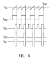
- FIG. 5 is a waveform diagram of the related signals of the electronic ballast in FIG. 2 corresponding to a dimming level.
- FIG. 2 shows a block diagram of a single-chip electronic ballast for driving a fluorescent lamp according to a preferred embodiment of the present invention.
- the electronic ballast comprises a line switching sensing circuit 201 , a counter 202 , a digital-to-analog converter 203 , an oscillator 204 , a comparator 205 , an AND-gate 206 , a combiner 207 and an inverter 208 .
- the line switching sensing circuit 201 is used to generate a switching sensing signal V CNT by performing a first voltage comparison operation on a DC voltage derived from a main input voltage V IN , and generate a reset signal RESET by counting the off time of the power line or by performing a second voltage comparison operation on a filtered DC voltage derived from the main input voltage V IN , wherein the first voltage comparison operation can be implemented with a comparator or a Schmitt trigger.
- the counter 202 is used to generate a digital count value B n B n . . . B 1 B 0 according to the switching sensing signal V CNT and the counter 202 is reset by the reset signal RESET.
- the digital-to-analog converter 203 is used to generate a first control voltage V C1 according to the digital count value B n B n . . . B 1 B 0 .
- the digital-to-analog converter 203 together with the counter 202 forms a control voltage generator, used to generate the first control voltage V C1 according to the digital count value B n B n-1 . . . B 1 B 0 of the switching sensing signal V CNT , and the control voltage generator is reset by the reset signal RESET when the off time of the power line exceeds a predetermined time.
- the oscillator 204 is used to generate a saw-tooth signal V SAW and an oscillating signal V OSC , wherein the saw-tooth signal V SAW , having a rising voltage portion and a falling voltage portion, is of a fixed frequency, for example but not limited to 45 Kh z , and the oscillating signal V OSC , a symmetric square signal, has a frequency equal to half of that of the saw-tooth signal V SAW .
- the comparator 205 , the AND-gate 206 , the combiner 207 and the inverter 208 are used to generate a high side gating signal V HS2 and a low side gating signal V LS according to the saw-tooth signal V SAW , the oscillating signal V OSC and the first control voltage V C1 , wherein the comparator 205 is used to generate a first high side gating signal V HS1 according to voltage comparison of the saw-tooth signal V SAW and a second control signal V C2 ; the AND-gate 206 is used to generate the high side gating signal V HS2 according to the logic-AND of the oscillating signal V OSC and the first high side gating signal V HS1 ; the combiner 207 is used to generate the second control signal V C2 by subtracting the first control signal V C1 with a bias voltage V b ; and the inverter 208 is used to generate the low side gating signal V LS according to the high side gating signal V
- the voltage of the second control signal V C2 which can be one of a plurality of discrete values, is used to determine a duty ratio of the first high side gating signal V HS1 in a way that, as the voltage of the second control signal V C2 is raised to a higher one, the duty ratio of the first high side gating signal V HS1 and the duty ratio of the high side gating signal V HS2 will be changed to a smaller one (for example, from 50% to 40%) and the luminance of the fluorescent lamp will thereby be dimmed to a lower value.
- the bias voltage V b is used to modify the duty ratio values of the high side gating signal V HS2 to provide a different set of luminance values.
- the digital count value of the counter 202 is represented by two bits, then there will be a level 0, a level 1, a level 2 and a level 3 of the dimming levels of the fluorescent lamp available, and let the relation between the dimming level, the luminance and the second control signal V C2 be as follows:
- the waveform of the related signals of the electronic ballast in FIG. 2 corresponding to a dimming level is shown in FIG. 5 .
- the frequency of V SAW is fixed and the frequency of V OSC is half of that of V SAW .
- the V SAW used to compare with the second control signal V C2 , has a rising voltage portion and a falling voltage portion, and the V OSC is a symmetric square signal.
- V SAW exceeds V C2
- the first high side gating signal V HS1 will exhibit high level and thereby exhibit a duty ratio.
- the high side gating signal V HS2 is the logic-AND result of V OSC and V HS1
- the low side gating signal V LS is generated according to the high side gating signal V HS2 .
- FIG. 3 a shows a block diagram of the line switching sensing circuit in FIG. 2 according to a preferred embodiment of the present invention.
- the preferred embodiment of the present invention at least includes a capacitor 301 , a resistor 302 , a resistor 303 , a comparator 304 , and a comparator 305 .
- the capacitor 301 is used to filter out the noise of the main input voltage V IN .
- the resistor 302 and the resistor 303 are used to act as a voltage divider to generate a DC voltage V X according to the main input voltage V IN .
- the comparator 304 is used to generate the switching sensing signal V CNT according to a sensing threshold voltage V TH and the DC voltage V X .
- the sensing threshold voltage V TH is preferably set, for example but not limited to 11V.
- FIG. 3 c shows the resulting waveform of V IN , V X , and V CNT when the lamp switch is consecutively switched on and off. As shown in FIG. 3 c , when V X falls below the sensing threshold voltage V TH , the switching sensing signal V CNT will change state from low to high; when V X rises above the sensing threshold voltage V TH , the switching sensing signal V CNT will change state from high to low.
- the comparator 305 is used to generate the reset signal RESET according to a reset threshold voltage V LOW and a filtered DC voltage V CC for the power supply of the comparator 305 , wherein the reset threshold voltage V LOW , for example but not limited to 6V, is greater than the minimum operation voltage of the ballast controller.
- the reset threshold voltage V LOW for example but not limited to 6V
- the filtered DC voltage V CC is gradually decreasing due to the charge stored in a bypass capacitor for the filtered DC voltage V CC . Therefore as the lamp switch is switched off, the filtered DC voltage V CC will not fall below the reset threshold voltage V LOW until the switch-off time exceeds a predetermined time, for example 1 sec, depending on the capacitance of the bypass capacitor.
- FIG. 3 b shows a block diagram of the line switching sensing circuit in FIG. 2 according to another preferred embodiment of the present invention.
- the preferred embodiment of the present invention at least includes a capacitor 301 , a resistor 302 , a resistor 303 , a comparator 304 , a delay unit 305 and an AND gate 306 .
- the capacitor 301 is used to filter out the noise of the main input voltage V IN .
- the resistor 302 and the resistor 303 are used to act as a voltage divider to generate a DC voltage V X according to the main input voltage V IN .
- the comparator 304 is used to generate the switching sensing signal V CNT according to a sensing threshold voltage V TH and the DC voltage V X .
- the sensing threshold voltage V TH is preferably set, for example but not limited to 11V.
- FIG. 3 c shows the resulting waveform of V IN , V X , and V CNT when the lamp switch is consecutively switched on and off. As shown in FIG. 3 c , when V X falls below the sensing threshold voltage V TH , the switching sensing signal V CNT will change state from low to high; when V X rises above the sensing threshold voltage V TH , the switching sensing signal V CNT will change state from high to low.
- the delay unit 305 is used to delay the switching sensing signal V CNT with the predetermined time to generate a delayed signal V CNTD .
- the AND gate 306 is used to generate the reset signal RESET according to the switching sensing signal V CNT and the delayed signal V CNTD .
- the reset signal RESET will stay low; when the pulse width of the switching sensing signal V CNT is longer than the predetermined time, the reset signal RESET will change state to high.
- FIG. 4 a shows a block diagram of the line switching sensing circuit in FIG. 2 according to still another preferred embodiment of the present invention.
- the preferred embodiment of the present invention at least includes a V CC start-up circuit 401 , a bypass capacitor 402 , a comparator 403 , a resistor 404 , a resistor 405 and a comparator 406 .
- the V CC start-up circuit 401 is used in generating the filtered DC voltage V CC according to the main input voltage V IN .
- the bypass capacitor 402 is used to filter out the noise of the filtered DC voltage V CC .
- the comparator 403 , the resistor 404 , and the resistor 405 are used to implement a Schmitt trigger to generate the switching sensing signal V CNT according to the voltage V CC .
- the low threshold voltage of the Schmitt trigger is set according to a UVLO (Under Voltage Lock Out) turn-off level, for example but not limited to 9V
- the high threshold voltage of the Schmitt trigger is set according to a UVLO turn-on level, for example but not limited to 13V.
- FIG. 4 c shows the resulting waveform of V IN , V CC and V CNT when the lamp switch is consecutively switched on and off.
- the comparator 406 is used to generate the reset signal RESET according to a reset threshold voltage V LOW and the filtered DC voltage V CC , wherein the reset threshold voltage V LOW , for example but not limited to 6V, is greater than the minimum operation voltage of the ballast controller.
- the reset threshold voltage V LOW for example but not limited to 6V
- the filtered DC voltage V CC is gradually decreasing due to the charge stored in the bypass capacitor 402 for the filtered DC voltage V CC . Therefore as the lamp switch is switched off, the filtered DC voltage V CC will not fall below the reset threshold voltage V LOW until the switch-off time exceeds a predetermined time, for example 1 sec, depending on the capacitance of the bypass capacitor 402 .
- FIG. 4 b shows a block diagram of the line switching sensing circuit in FIG. 2 according to still another preferred embodiment of the present invention.
- the preferred embodiment of the present invention at least includes a V CC start-up circuit 401 , a bypass capacitor 402 , a comparator 403 , a resistor 404 , a resistor 405 a delay unit 406 and an AND gate 407 .
- the V CC start-up circuit 401 is used in generating the filtered DC voltage V CC according to the main input voltage V IN .
- the bypass capacitor 402 is used to filter out the noise of the filtered DC voltage V CC .
- the comparator 403 , the resistor 404 , and the resistor 405 are used to implement a Schmitt trigger to generate the switching sensing signal V CNT according to the voltage V CC .
- the low threshold voltage of the Schmitt trigger is set according to a UVLO (Under Voltage Lock Out) turn-off level, for example but not limited to 9V
- the high threshold voltage of the Schmitt trigger is set according to a UVLO turn-on level, for example but not limited to 13V.
- FIG. 4 c shows the resulting waveform of V IN , V CC and V CNT when the lamp switch is consecutively switched on and off.
- the delay unit 406 is used to delay the switching sensing signal V CNT with the predetermined time to generate a delayed signal V CNTD .
- the AND gate 407 is used to generate the reset signal RESET according to the switching sensing signal V CNT and the delayed signal V CNTD .
- the reset signal RESET will stay low; when the pulse width of the switching sensing signal V CNT is longer than the predetermined time, the reset signal RESET will change state to high.
- the present invention herein enhances the performance than the conventional structure and further complies with the patent application requirements and is submitted to the Patent and Trademark Office for review and granting of the commensurate patent rights.
Abstract
The present invention discloses an electronic ballast with dimming control from power line sensing for a fluorescent lamp, comprising: a control voltage generator, used to generate a control voltage according to a switching count of a power line; an oscillator, used to generate an oscillating signal, wherein the oscillating signal is of a fixed frequency and has a rising voltage portion and a falling voltage portion; and a comparator, used to generate a high side gating signal according to voltage comparison of the oscillating signal and the control voltage.
Description
1. Field of the Invention
The present invention relates to electronic ballasts, and more particularly to electronic ballasts with dimming control from power line sensing.
2. Description of the Related Art
In supplying power to gas-discharge lamps such as fluorescent lamps or cold cathode fluorescent lamps or compact fluorescent lamps, electronic ballasts are widely adopted to keep the lamp current stable.
In the architecture, the full bridge rectifier 101 is used to rectify an AC line input voltage to generate a main input voltage VIN.
The VCC start-up circuit 102, coupling to the main input voltage VIN, is used to start up the generation of a DC voltage VCC.
The ballast control IC 103 is used to generate a high side driving signal VHS for driving the NMOS transistor 104 and a low side driving signal VLS for driving the NMOS transistor 105 to deliver a current ILMP to the fluorescent lamp, in response to the voltage at the DIM input pin 3.
The NMOS transistor 104 and the NMOS transistor 105 are used for generating a square waveform to a LC resonant network. The LC resonant network then converts the square waveform to a current signal ILMP to drive the lamp.
The voltage divider 106 is coupled to a 110V DIM input to generate a DIM control voltage at the DIM input pin 3 of the ballast control IC 103. The 110V DIM input is an additional port to the electronic ballast. In the prior art, the 110V DIM input is generally coupled to an additional dial switch (wall dimmer) or a remote control means, and users have to operate the additional dial switch or the remote control means other than an existing lamp rocker switch to trigger the electronic ballast to adjust the luminance of the lamp.
Through the setting of the DIM input, the NMOS transistor 104 and the NMOS transistor 105 are periodically switched on-and-off by the high side driving signal VHS and the low side driving signal VLS respectively, and the input power is transformed from the main input voltage VIN to the lamp in the form of a current signal ILMP of which the root-mean-square value is corresponding to the setting of the DIM input.
However, since the setting of the DIM input in the prior art has to be done by manipulating an additional dial switch or a remote control means other than an existing lamp switch, users have to pay more cost for the additional dial switch or remote control means. Besides, the additional dial switch may have to be mounted on the wall wherein the wiring between the dial switch and the ballast is bothersome. As to the remote control means, the communication between the transmitter and the receiver needs power, and if the remote control means runs out of battery, then there is no way to dim the lamp unless the battery is replaced.
Therefore, there is a need to provide a solution capable of reducing the cost and eliminating the need of an additional dial switch or remote control means in implementing an electronic ballast with dimming function.
Seeing this bottleneck, the present invention proposes a novel topology of electronic ballast capable of dimming the fluorescent lamp by adjusting the duty ratio of a fixed-frequency square signal according to the count of switching of a corresponding lamp switch, without the need of any additional dial switch or remote control means.
One objective of the present invention is to provide an electronic ballast with dimming control from power line sensing which does not need any additional dial switch or remote control means in the luminance adjustment of the lamp.
Another objective of the present invention is to provide an electronic ballast with dimming function which is accomplished by adjusting the duty ratio of a fixed-frequency square signal according to the count of switching of a corresponding lamp switch.
Still another objective of the present invention is to provide a fully integrated single chip electronic ballast with concise architecture which can control the luminance of the lamp by adjusting the duty ratio of a fixed-frequency square signal according to a switching count of a corresponding lamp switch.
To achieve the foregoing objectives, the present invention provides an electronic ballast with dimming control from power line sensing for a fluorescent lamp, comprising: a control voltage generator, used to generate a control voltage according to a switching count of a power line; an oscillator, used to generate a first oscillating signal and a second oscillating signal, wherein the first oscillating signal is of a fixed frequency and has a rising voltage portion and a falling voltage portion, and the second oscillating signal is a square signal of which the frequency is half of that of the first oscillating signal; a comparator, used to generate a first high side gating signal according to voltage comparison of the first oscillating signal and the control voltage; and an AND gate, used to generate a high side gating signal according to the first high side gating signal and the second oscillating signal.
To make it easier for our examiner to understand the objective of the invention, its structure, innovative features, and performance, we use preferred embodiments together with the accompanying drawings for the detailed description of the invention.
The present invention will be described in more detail hereinafter with reference to the accompanying drawings that show the preferred embodiment of the invention.
Please refer to FIG. 2 , which shows a block diagram of a single-chip electronic ballast for driving a fluorescent lamp according to a preferred embodiment of the present invention. As shown in FIG. 2 , the electronic ballast comprises a line switching sensing circuit 201, a counter 202, a digital-to-analog converter 203, an oscillator 204, a comparator 205, an AND-gate 206, a combiner 207 and an inverter 208.
The line switching sensing circuit 201 is used to generate a switching sensing signal VCNT by performing a first voltage comparison operation on a DC voltage derived from a main input voltage VIN, and generate a reset signal RESET by counting the off time of the power line or by performing a second voltage comparison operation on a filtered DC voltage derived from the main input voltage VIN, wherein the first voltage comparison operation can be implemented with a comparator or a Schmitt trigger.
The counter 202 is used to generate a digital count value BnBn . . . B1B0 according to the switching sensing signal VCNT and the counter 202 is reset by the reset signal RESET.
The digital-to-analog converter 203 is used to generate a first control voltage VC1 according to the digital count value BnBn . . . B1B0. The digital-to-analog converter 203 together with the counter 202 forms a control voltage generator, used to generate the first control voltage VC1 according to the digital count value BnBn-1 . . . B1B0 of the switching sensing signal VCNT, and the control voltage generator is reset by the reset signal RESET when the off time of the power line exceeds a predetermined time.
The oscillator 204 is used to generate a saw-tooth signal VSAW and an oscillating signal VOSC, wherein the saw-tooth signal VSAW, having a rising voltage portion and a falling voltage portion, is of a fixed frequency, for example but not limited to 45 Khz, and the oscillating signal VOSC, a symmetric square signal, has a frequency equal to half of that of the saw-tooth signal VSAW.
The comparator 205, the AND-gate 206, the combiner 207 and the inverter 208 are used to generate a high side gating signal VHS2 and a low side gating signal VLS according to the saw-tooth signal VSAW, the oscillating signal VOSC and the first control voltage VC1, wherein the comparator 205 is used to generate a first high side gating signal VHS1 according to voltage comparison of the saw-tooth signal VSAW and a second control signal VC2; the AND-gate 206 is used to generate the high side gating signal VHS2 according to the logic-AND of the oscillating signal VOSC and the first high side gating signal VHS1; the combiner 207 is used to generate the second control signal VC2 by subtracting the first control signal VC1 with a bias voltage Vb; and the inverter 208 is used to generate the low side gating signal VLS according to the high side gating signal VHS2. The voltage of the second control signal VC2, which can be one of a plurality of discrete values, is used to determine a duty ratio of the first high side gating signal VHS1 in a way that, as the voltage of the second control signal VC2 is raised to a higher one, the duty ratio of the first high side gating signal VHS1 and the duty ratio of the high side gating signal VHS2 will be changed to a smaller one (for example, from 50% to 40%) and the luminance of the fluorescent lamp will thereby be dimmed to a lower value. The bias voltage Vb is used to modify the duty ratio values of the high side gating signal VHS2 to provide a different set of luminance values. For example, if the digital count value of the counter 202 is represented by two bits, then there will be a level 0, a level 1, a level 2 and a level 3 of the dimming levels of the fluorescent lamp available, and let the relation between the dimming level, the luminance and the second control signal VC2 be as follows:
| Dimming level | |||
| Level 0 | | | Level 3 | ||
| VC2 | 0 V | 1 V | 2 V | 3 V | ||
| Luminance, | 100% | 75% | 50% | 25% | ||
then a value of the bias voltage Vb will reduce the voltage of the VC2 to provide a different luminance profile.
The waveform of the related signals of the electronic ballast in FIG. 2 corresponding to a dimming level is shown in FIG. 5 . As shown in FIG. 5 , the frequency of VSAW is fixed and the frequency of VOSC is half of that of VSAW. The VSAW, used to compare with the second control signal VC2, has a rising voltage portion and a falling voltage portion, and the VOSC is a symmetric square signal. When VSAW exceeds VC2, the first high side gating signal VHS1 will exhibit high level and thereby exhibit a duty ratio. The high side gating signal VHS2 is the logic-AND result of VOSC and VHS1, and the low side gating signal VLS is generated according to the high side gating signal VHS2.
Please refer to FIG. 3 a, which shows a block diagram of the line switching sensing circuit in FIG. 2 according to a preferred embodiment of the present invention. As shown in FIG. 3 a, the preferred embodiment of the present invention at least includes a capacitor 301, a resistor 302, a resistor 303, a comparator 304, and a comparator 305.
The capacitor 301 is used to filter out the noise of the main input voltage VIN.
The resistor 302 and the resistor 303 are used to act as a voltage divider to generate a DC voltage VX according to the main input voltage VIN.
The comparator 304 is used to generate the switching sensing signal VCNT according to a sensing threshold voltage VTH and the DC voltage VX. The sensing threshold voltage VTH, is preferably set, for example but not limited to 11V. FIG. 3 c shows the resulting waveform of VIN, VX, and VCNT when the lamp switch is consecutively switched on and off. As shown in FIG. 3 c, when VX falls below the sensing threshold voltage VTH, the switching sensing signal VCNT will change state from low to high; when VX rises above the sensing threshold voltage VTH, the switching sensing signal VCNT will change state from high to low.
The comparator 305 is used to generate the reset signal RESET according to a reset threshold voltage VLOW and a filtered DC voltage VCC for the power supply of the comparator 305, wherein the reset threshold voltage VLOW, for example but not limited to 6V, is greater than the minimum operation voltage of the ballast controller. When the lamp switch is switched off, the main input voltage VIN will be pulled down immediately, but meanwhile the filtered DC voltage VCC is gradually decreasing due to the charge stored in a bypass capacitor for the filtered DC voltage VCC. Therefore as the lamp switch is switched off, the filtered DC voltage VCC will not fall below the reset threshold voltage VLOW until the switch-off time exceeds a predetermined time, for example 1 sec, depending on the capacitance of the bypass capacitor.
Please refer to FIG. 3 b, which shows a block diagram of the line switching sensing circuit in FIG. 2 according to another preferred embodiment of the present invention. As shown in FIG. 3 b, the preferred embodiment of the present invention at least includes a capacitor 301, a resistor 302, a resistor 303, a comparator 304, a delay unit 305 and an AND gate 306.
The capacitor 301 is used to filter out the noise of the main input voltage VIN.
The resistor 302 and the resistor 303 are used to act as a voltage divider to generate a DC voltage VX according to the main input voltage VIN.
The comparator 304 is used to generate the switching sensing signal VCNT according to a sensing threshold voltage VTH and the DC voltage VX. The sensing threshold voltage VTH, is preferably set, for example but not limited to 11V. FIG. 3 c shows the resulting waveform of VIN, VX, and VCNT when the lamp switch is consecutively switched on and off. As shown in FIG. 3 c, when VX falls below the sensing threshold voltage VTH, the switching sensing signal VCNT will change state from low to high; when VX rises above the sensing threshold voltage VTH, the switching sensing signal VCNT will change state from high to low.
The delay unit 305 is used to delay the switching sensing signal VCNT with the predetermined time to generate a delayed signal VCNTD.
The AND gate 306 is used to generate the reset signal RESET according to the switching sensing signal VCNT and the delayed signal VCNTD. When the pulse width of the switching sensing signal VCNT is shorter than the predetermined time, the reset signal RESET will stay low; when the pulse width of the switching sensing signal VCNT is longer than the predetermined time, the reset signal RESET will change state to high.
The VCC start-up circuit 401 is used in generating the filtered DC voltage VCC according to the main input voltage VIN.
The bypass capacitor 402 is used to filter out the noise of the filtered DC voltage VCC.
The comparator 403, the resistor 404, and the resistor 405 are used to implement a Schmitt trigger to generate the switching sensing signal VCNT according to the voltage VCC. The low threshold voltage of the Schmitt trigger is set according to a UVLO (Under Voltage Lock Out) turn-off level, for example but not limited to 9V, and the high threshold voltage of the Schmitt trigger is set according to a UVLO turn-on level, for example but not limited to 13V. FIG. 4 c shows the resulting waveform of VIN, VCC and VCNT when the lamp switch is consecutively switched on and off. When VCC falls below the UVLO turn-off level, the switching sensing signal Vcnt will change state from low to high; when VCC rises beyond the UVLO turn-on level, the switching sensing signal VCNT will change state from high to low.
The comparator 406 is used to generate the reset signal RESET according to a reset threshold voltage VLOW and the filtered DC voltage VCC, wherein the reset threshold voltage VLOW, for example but not limited to 6V, is greater than the minimum operation voltage of the ballast controller. When the lamp switch is switched off, the main input voltage VIN will be pulled down immediately, but meanwhile the filtered DC voltage VCC is gradually decreasing due to the charge stored in the bypass capacitor 402 for the filtered DC voltage VCC. Therefore as the lamp switch is switched off, the filtered DC voltage VCC will not fall below the reset threshold voltage VLOW until the switch-off time exceeds a predetermined time, for example 1 sec, depending on the capacitance of the bypass capacitor 402.
The VCC start-up circuit 401 is used in generating the filtered DC voltage VCC according to the main input voltage VIN.
The bypass capacitor 402 is used to filter out the noise of the filtered DC voltage VCC.
The comparator 403, the resistor 404, and the resistor 405 are used to implement a Schmitt trigger to generate the switching sensing signal VCNT according to the voltage VCC. The low threshold voltage of the Schmitt trigger is set according to a UVLO (Under Voltage Lock Out) turn-off level, for example but not limited to 9V, and the high threshold voltage of the Schmitt trigger is set according to a UVLO turn-on level, for example but not limited to 13V. FIG. 4 c shows the resulting waveform of VIN, VCC and VCNT when the lamp switch is consecutively switched on and off. When VCC falls below the UVLO turn-off level, the switching sensing signal Vcnt will change state from low to high; when VCC rises beyond the UVLO turn-on level, the switching sensing signal VCNT will change state from high to low.
The delay unit 406 is used to delay the switching sensing signal VCNT with the predetermined time to generate a delayed signal VCNTD. The AND gate 407 is used to generate the reset signal RESET according to the switching sensing signal VCNT and the delayed signal VCNTD. When the pulse width of the switching sensing signal VCNT is shorter than the predetermined time, the reset signal RESET will stay low; when the pulse width of the switching sensing signal VCNT is longer than the predetermined time, the reset signal RESET will change state to high.
Through the implementation of the present invention, a fully integrated single-chip electronic ballast capable of dimming control of a fluorescent lamp by sensing the count of switching of a lamp switch is presented. The topology of the present invention is much more concise than prior art circuits, so the present invention does conquer the disadvantages of prior art circuits.
While the invention has been described by way of examples and in terms of preferred embodiments, it is to be understood that the invention is not limited thereto. To the contrary, it is intended to cover various modifications and similar arrangements and procedures, and the scope of the appended claims therefore should be accorded the broadest interpretation so as to encompass all such modifications and similar arrangements and procedures.
In summation of the above description, the present invention herein enhances the performance than the conventional structure and further complies with the patent application requirements and is submitted to the Patent and Trademark Office for review and granting of the commensurate patent rights.
Claims (10)
1. An electronic ballast with dimming control from power line sensing for a fluorescent lamp, comprising:
a control voltage generator, used to generate a control voltage according to a switching count of a power line;
an oscillator, used to generate a first oscillating signal, wherein said first oscillating signal is of a fixed frequency and has a rising voltage portion and a falling voltage portion; and
a comparator, used to generate a high side gating signal according to voltage comparison of said first oscillating signal and said control voltage.
2. The electronic ballast with dimming control from power line sensing as claim 1 , wherein said control voltage generator comprises:
a line switching sensing circuit, used to generate a line switching sensing signal by sensing the voltage of said power line;
a counter, used to generate a digital count value according to said switching sensing signal; and
a digital-to-analog converter, used to generate said control voltage according to said digital count value.
3. The electronic ballast with dimming control from power line sensing as claim 2 , wherein said line switching sensing circuit comprises:
a capacitor, used to filter out a noise of said power line;
a voltage divider, used to generate a DC voltage according to said power line;
a comparator, used to generate said switching sensing signal according to said DC voltage and a sensing threshold voltage.
4. The electronic ballast with dimming control from power line sensing as claim 2 , wherein said line switching sensing circuit comprises:
a start-up circuit, used in generating a filtered DC voltage according to said power line;
a capacitor, used to filter out a noise of said filtered DC voltage;
a Schmitt trigger, used to generate said switching sensing signal according to said filtered DC voltage, wherein said Schmitt trigger has a high threshold voltage corresponding to a UVLO turn-on level, and a low threshold voltage corresponding to a UVLO turn-off level.
5. The electronic ballast with dimming control from power line sensing as claim 1 , wherein said control voltage generator comprises:
a line switching sensing circuit, used to generate a line switching sensing signal by sensing the voltage of said power line;
a counter, used to generate a digital count value according to said switching sensing signal;
a digital-to-analog converter, used to generate a first control voltage according to said digital count value; and
a combiner, used to combine said first control voltage with a bias voltage to generate said control voltage.
6. An electronic ballast with dimming control from power line sensing for a fluorescent lamp, wherein said electronic ballast is integrated in a single chip, said electronic ballast comprising:
a control voltage generator, used to generate a control voltage according to a switching count of a power line;
an oscillator, used to generate a first oscillating signal and a second oscillating signal, wherein said first oscillating signal is of a fixed frequency and has a rising voltage portion and a falling voltage portion, and said second oscillating signal is a square signal of which the frequency is half of that of said first oscillating signal;
a comparator, used to generate a first high side gating signal according to voltage comparison of said first oscillating signal and said control voltage; and
an AND gate, used to generate a high side gating signal according to said first high side gating signal and said second oscillating signal.
7. The electronic ballast with dimming control from power line sensing as claim 6 , wherein said control voltage generator comprises:
a line switching sensing circuit, used to generate a line switching sensing signal by sensing the voltage of said power line;
a counter, used to generate a digital count value according to said switching sensing signal; and
a digital-to-analog converter, used to generate said control voltage according to said digital count value.
8. The electronic ballast with dimming control from power line sensing as claim 6 , further comprising an inverter, which is used to invert said high side gating signal to generate a low side gating signal.
9. The electronic ballast with dimming control from power line sensing as claim 6 , wherein said control voltage generator comprises:
a line switching sensing circuit, used to generate a line switching sensing signal by sensing the voltage of said power line;
a counter, used to generate a digital count value according to said switching sensing signal;
a digital-to-analog converter, used to generate a first control voltage according to said digital count value; and
a combiner, used to combine said first control voltage with a bias voltage to generate said control voltage.
10. The electronic ballast with dimming control from power line sensing as claim 6 , wherein said first oscillating signal is a saw-tooth signal.
Priority Applications (1)
| Application Number | Priority Date | Filing Date | Title |
|---|---|---|---|
| US12/505,731 US8067904B2 (en) | 2009-07-20 | 2009-07-20 | Electronic ballast with dimming control from power line sensing |
Applications Claiming Priority (1)
| Application Number | Priority Date | Filing Date | Title |
|---|---|---|---|
| US12/505,731 US8067904B2 (en) | 2009-07-20 | 2009-07-20 | Electronic ballast with dimming control from power line sensing |
Publications (2)
| Publication Number | Publication Date |
|---|---|
| US20110012536A1 US20110012536A1 (en) | 2011-01-20 |
| US8067904B2 true US8067904B2 (en) | 2011-11-29 |
Family
ID=43464793
Family Applications (1)
| Application Number | Title | Priority Date | Filing Date |
|---|---|---|---|
| US12/505,731 Expired - Fee Related US8067904B2 (en) | 2009-07-20 | 2009-07-20 | Electronic ballast with dimming control from power line sensing |
Country Status (1)
| Country | Link |
|---|---|
| US (1) | US8067904B2 (en) |
Cited By (1)
| Publication number | Priority date | Publication date | Assignee | Title |
|---|---|---|---|---|
| US8928255B2 (en) | 2013-03-07 | 2015-01-06 | Osram Sylvania Inc. | Dynamic step dimming interface |
Families Citing this family (3)
| Publication number | Priority date | Publication date | Assignee | Title |
|---|---|---|---|---|
| CN106535412B (en) * | 2016-12-21 | 2018-07-10 | 贵州恒芯微电子科技有限公司 | The digital simulation light adjusting circuit that a kind of port shares |
| EP3562272B1 (en) | 2017-05-27 | 2022-09-07 | Lee, Yu-Lin | Drive system |
| TWI687132B (en) | 2018-05-03 | 2020-03-01 | 李玉麟 | Driver device |
Citations (4)
| Publication number | Priority date | Publication date | Assignee | Title |
|---|---|---|---|---|
| US5798620A (en) * | 1996-12-17 | 1998-08-25 | Philips Electronics North America Corporation | Fluorescent lamp dimming |
| US7126288B2 (en) * | 2003-05-05 | 2006-10-24 | International Rectifier Corporation | Digital electronic ballast control apparatus and method |
| US7414371B1 (en) * | 2005-11-21 | 2008-08-19 | Microsemi Corporation | Voltage regulation loop with variable gain control for inverter circuit |
| US20110169425A1 (en) * | 2010-01-14 | 2011-07-14 | Grenergy Opto, Inc. | Single chip ballast controller for step-dimming of a fluorescent lamp |
-
2009
- 2009-07-20 US US12/505,731 patent/US8067904B2/en not_active Expired - Fee Related
Patent Citations (4)
| Publication number | Priority date | Publication date | Assignee | Title |
|---|---|---|---|---|
| US5798620A (en) * | 1996-12-17 | 1998-08-25 | Philips Electronics North America Corporation | Fluorescent lamp dimming |
| US7126288B2 (en) * | 2003-05-05 | 2006-10-24 | International Rectifier Corporation | Digital electronic ballast control apparatus and method |
| US7414371B1 (en) * | 2005-11-21 | 2008-08-19 | Microsemi Corporation | Voltage regulation loop with variable gain control for inverter circuit |
| US20110169425A1 (en) * | 2010-01-14 | 2011-07-14 | Grenergy Opto, Inc. | Single chip ballast controller for step-dimming of a fluorescent lamp |
Cited By (1)
| Publication number | Priority date | Publication date | Assignee | Title |
|---|---|---|---|---|
| US8928255B2 (en) | 2013-03-07 | 2015-01-06 | Osram Sylvania Inc. | Dynamic step dimming interface |
Also Published As
| Publication number | Publication date |
|---|---|
| US20110012536A1 (en) | 2011-01-20 |
Similar Documents
| Publication | Publication Date | Title |
|---|---|---|
| US7982413B2 (en) | Electronic ballast with dimming control from power line sensing | |
| US7075251B2 (en) | Universal platform for phase dimming discharge lighting ballast and lamp | |
| US8698414B2 (en) | High resolution pulse width modulation (PWM) frequency control using a tunable oscillator | |
| US20100295478A1 (en) | Led driving circuit | |
| KR20120081610A (en) | Dimming of led driver | |
| US9485817B2 (en) | Control circuit of light emitting element | |
| WO2011002600A1 (en) | Integrated backlight control system | |
| EP1296543B1 (en) | Circuit arrangement | |
| CA2271446C (en) | Circuit arrangement for operating electrical lamps | |
| JP5340719B2 (en) | Light emitting element control circuit, light emitting device using the same, and liquid crystal display device | |
| US8067904B2 (en) | Electronic ballast with dimming control from power line sensing | |
| US7129648B2 (en) | Interface circuit for operating capacitive loads | |
| US4933606A (en) | Discharge lamp driving method and electronic operators for implementation of the same | |
| US8084953B2 (en) | Changing power input to a gas discharge lamp | |
| US7999494B2 (en) | Electronic ballast with dimming control from power line sensing | |
| TWI613931B (en) | Electronic control gears for led light engine and application thereof | |
| CN113543411B (en) | Current limiting circuit and application thereof | |
| CN211378326U (en) | But LED drive circuit of switch control of adjusting luminance | |
| US7999495B2 (en) | Electronic ballast with dimming control from power line sensing | |
| CN112369125B (en) | LED driver and LED lighting system for use with high frequency electronic ballasts | |
| US20110169425A1 (en) | Single chip ballast controller for step-dimming of a fluorescent lamp | |
| CN106793348B (en) | Multifunctional LED dims Dolby circuit and LED dimming power sources | |
| CN111194119A (en) | LED driving circuit and method capable of being controlled by switching and dimming | |
| US20130043800A1 (en) | Power converter and a dimmable solid-state lighting device with the power converter | |
| TWI410175B (en) | An electronic ballast that senses the brightness of the power line |
Legal Events
| Date | Code | Title | Description |
|---|---|---|---|
| AS | Assignment |
Owner name: GRENERGY OPTO, INC., TAIWAN Free format text: ASSIGNMENT OF ASSIGNORS INTEREST;ASSIGNORS:LIN, KO-MING;WANG, YEN-PING;CHEN, PEI-YUAN;AND OTHERS;SIGNING DATES FROM 20090611 TO 20090615;REEL/FRAME:022976/0628 |
|
| REMI | Maintenance fee reminder mailed | ||
| LAPS | Lapse for failure to pay maintenance fees | ||
| STCH | Information on status: patent discontinuation |
Free format text: PATENT EXPIRED DUE TO NONPAYMENT OF MAINTENANCE FEES UNDER 37 CFR 1.362 |
|
| FP | Expired due to failure to pay maintenance fee |
Effective date: 20151129 |