US8071450B2 - Method for forming voltage sustaining layer with opposite-doped islands for semiconductor power devices - Google Patents
Method for forming voltage sustaining layer with opposite-doped islands for semiconductor power devices Download PDFInfo
- Publication number
- US8071450B2 US8071450B2 US12/355,165 US35516509A US8071450B2 US 8071450 B2 US8071450 B2 US 8071450B2 US 35516509 A US35516509 A US 35516509A US 8071450 B2 US8071450 B2 US 8071450B2
- Authority
- US
- United States
- Prior art keywords
- sustaining layer
- voltage
- epitaxial layer
- voltage sustaining
- layer
- Prior art date
- Legal status (The legal status is an assumption and is not a legal conclusion. Google has not performed a legal analysis and makes no representation as to the accuracy of the status listed.)
- Expired - Fee Related, expires
Links
- 239000004065 semiconductor Substances 0.000 title claims abstract description 14
- 238000000034 method Methods 0.000 title claims abstract description 11
- 239000000758 substrate Substances 0.000 claims abstract description 11
- 230000000873 masking effect Effects 0.000 claims abstract 3
- 238000004519 manufacturing process Methods 0.000 claims abstract 2
- 230000015556 catabolic process Effects 0.000 description 8
- 230000008569 process Effects 0.000 description 7
- XUIMIQQOPSSXEZ-UHFFFAOYSA-N Silicon Chemical compound [Si] XUIMIQQOPSSXEZ-UHFFFAOYSA-N 0.000 description 4
- 229910052710 silicon Inorganic materials 0.000 description 4
- 239000010703 silicon Substances 0.000 description 4
- 238000002347 injection Methods 0.000 description 3
- 239000007924 injection Substances 0.000 description 3
- 230000004907 flux Effects 0.000 description 2
- 238000012986 modification Methods 0.000 description 2
- 230000004048 modification Effects 0.000 description 2
- ZOXJGFHDIHLPTG-UHFFFAOYSA-N Boron Chemical compound [B] ZOXJGFHDIHLPTG-UHFFFAOYSA-N 0.000 description 1
- 239000000370 acceptor Substances 0.000 description 1
- 229910052796 boron Inorganic materials 0.000 description 1
- 239000000969 carrier Substances 0.000 description 1
- 230000008859 change Effects 0.000 description 1
- 238000013461 design Methods 0.000 description 1
- 238000010586 diagram Methods 0.000 description 1
- 238000009792 diffusion process Methods 0.000 description 1
- 230000000694 effects Effects 0.000 description 1
- 238000005516 engineering process Methods 0.000 description 1
- 230000006872 improvement Effects 0.000 description 1
- 239000012535 impurity Substances 0.000 description 1
- 230000006698 induction Effects 0.000 description 1
- 238000011835 investigation Methods 0.000 description 1
- 229910044991 metal oxide Inorganic materials 0.000 description 1
- 150000004706 metal oxides Chemical class 0.000 description 1
- 238000011160 research Methods 0.000 description 1
- 238000004088 simulation Methods 0.000 description 1
- 230000003068 static effect Effects 0.000 description 1
Images


Classifications
-
- H—ELECTRICITY
- H01—ELECTRIC ELEMENTS
- H01L—SEMICONDUCTOR DEVICES NOT COVERED BY CLASS H10
- H01L29/00—Semiconductor devices adapted for rectifying, amplifying, oscillating or switching, or capacitors or resistors with at least one potential-jump barrier or surface barrier, e.g. PN junction depletion layer or carrier concentration layer; Details of semiconductor bodies or of electrodes thereof ; Multistep manufacturing processes therefor
- H01L29/66—Types of semiconductor device ; Multistep manufacturing processes therefor
- H01L29/68—Types of semiconductor device ; Multistep manufacturing processes therefor controllable by only the electric current supplied, or only the electric potential applied, to an electrode which does not carry the current to be rectified, amplified or switched
- H01L29/76—Unipolar devices, e.g. field effect transistors
- H01L29/772—Field effect transistors
- H01L29/78—Field effect transistors with field effect produced by an insulated gate
- H01L29/7801—DMOS transistors, i.e. MISFETs with a channel accommodating body or base region adjoining a drain drift region
- H01L29/7802—Vertical DMOS transistors, i.e. VDMOS transistors
-
- H—ELECTRICITY
- H01—ELECTRIC ELEMENTS
- H01L—SEMICONDUCTOR DEVICES NOT COVERED BY CLASS H10
- H01L29/00—Semiconductor devices adapted for rectifying, amplifying, oscillating or switching, or capacitors or resistors with at least one potential-jump barrier or surface barrier, e.g. PN junction depletion layer or carrier concentration layer; Details of semiconductor bodies or of electrodes thereof ; Multistep manufacturing processes therefor
- H01L29/02—Semiconductor bodies ; Multistep manufacturing processes therefor
- H01L29/06—Semiconductor bodies ; Multistep manufacturing processes therefor characterised by their shape; characterised by the shapes, relative sizes, or dispositions of the semiconductor regions ; characterised by the concentration or distribution of impurities within semiconductor regions
- H01L29/0603—Semiconductor bodies ; Multistep manufacturing processes therefor characterised by their shape; characterised by the shapes, relative sizes, or dispositions of the semiconductor regions ; characterised by the concentration or distribution of impurities within semiconductor regions characterised by particular constructional design considerations, e.g. for preventing surface leakage, for controlling electric field concentration or for internal isolations regions
- H01L29/0607—Semiconductor bodies ; Multistep manufacturing processes therefor characterised by their shape; characterised by the shapes, relative sizes, or dispositions of the semiconductor regions ; characterised by the concentration or distribution of impurities within semiconductor regions characterised by particular constructional design considerations, e.g. for preventing surface leakage, for controlling electric field concentration or for internal isolations regions for preventing surface leakage or controlling electric field concentration
- H01L29/0611—Semiconductor bodies ; Multistep manufacturing processes therefor characterised by their shape; characterised by the shapes, relative sizes, or dispositions of the semiconductor regions ; characterised by the concentration or distribution of impurities within semiconductor regions characterised by particular constructional design considerations, e.g. for preventing surface leakage, for controlling electric field concentration or for internal isolations regions for preventing surface leakage or controlling electric field concentration for increasing or controlling the breakdown voltage of reverse biased devices
- H01L29/0615—Semiconductor bodies ; Multistep manufacturing processes therefor characterised by their shape; characterised by the shapes, relative sizes, or dispositions of the semiconductor regions ; characterised by the concentration or distribution of impurities within semiconductor regions characterised by particular constructional design considerations, e.g. for preventing surface leakage, for controlling electric field concentration or for internal isolations regions for preventing surface leakage or controlling electric field concentration for increasing or controlling the breakdown voltage of reverse biased devices by the doping profile or the shape or the arrangement of the PN junction, or with supplementary regions, e.g. junction termination extension [JTE]
- H01L29/0619—Semiconductor bodies ; Multistep manufacturing processes therefor characterised by their shape; characterised by the shapes, relative sizes, or dispositions of the semiconductor regions ; characterised by the concentration or distribution of impurities within semiconductor regions characterised by particular constructional design considerations, e.g. for preventing surface leakage, for controlling electric field concentration or for internal isolations regions for preventing surface leakage or controlling electric field concentration for increasing or controlling the breakdown voltage of reverse biased devices by the doping profile or the shape or the arrangement of the PN junction, or with supplementary regions, e.g. junction termination extension [JTE] with a supplementary region doped oppositely to or in rectifying contact with the semiconductor containing or contacting region, e.g. guard rings with PN or Schottky junction
- H01L29/0623—Buried supplementary region, e.g. buried guard ring
-
- H—ELECTRICITY
- H01—ELECTRIC ELEMENTS
- H01L—SEMICONDUCTOR DEVICES NOT COVERED BY CLASS H10
- H01L29/00—Semiconductor devices adapted for rectifying, amplifying, oscillating or switching, or capacitors or resistors with at least one potential-jump barrier or surface barrier, e.g. PN junction depletion layer or carrier concentration layer; Details of semiconductor bodies or of electrodes thereof ; Multistep manufacturing processes therefor
- H01L29/02—Semiconductor bodies ; Multistep manufacturing processes therefor
- H01L29/06—Semiconductor bodies ; Multistep manufacturing processes therefor characterised by their shape; characterised by the shapes, relative sizes, or dispositions of the semiconductor regions ; characterised by the concentration or distribution of impurities within semiconductor regions
- H01L29/0603—Semiconductor bodies ; Multistep manufacturing processes therefor characterised by their shape; characterised by the shapes, relative sizes, or dispositions of the semiconductor regions ; characterised by the concentration or distribution of impurities within semiconductor regions characterised by particular constructional design considerations, e.g. for preventing surface leakage, for controlling electric field concentration or for internal isolations regions
- H01L29/0607—Semiconductor bodies ; Multistep manufacturing processes therefor characterised by their shape; characterised by the shapes, relative sizes, or dispositions of the semiconductor regions ; characterised by the concentration or distribution of impurities within semiconductor regions characterised by particular constructional design considerations, e.g. for preventing surface leakage, for controlling electric field concentration or for internal isolations regions for preventing surface leakage or controlling electric field concentration
- H01L29/0611—Semiconductor bodies ; Multistep manufacturing processes therefor characterised by their shape; characterised by the shapes, relative sizes, or dispositions of the semiconductor regions ; characterised by the concentration or distribution of impurities within semiconductor regions characterised by particular constructional design considerations, e.g. for preventing surface leakage, for controlling electric field concentration or for internal isolations regions for preventing surface leakage or controlling electric field concentration for increasing or controlling the breakdown voltage of reverse biased devices
- H01L29/0615—Semiconductor bodies ; Multistep manufacturing processes therefor characterised by their shape; characterised by the shapes, relative sizes, or dispositions of the semiconductor regions ; characterised by the concentration or distribution of impurities within semiconductor regions characterised by particular constructional design considerations, e.g. for preventing surface leakage, for controlling electric field concentration or for internal isolations regions for preventing surface leakage or controlling electric field concentration for increasing or controlling the breakdown voltage of reverse biased devices by the doping profile or the shape or the arrangement of the PN junction, or with supplementary regions, e.g. junction termination extension [JTE]
- H01L29/063—Reduced surface field [RESURF] pn-junction structures
- H01L29/0634—Multiple reduced surface field (multi-RESURF) structures, e.g. double RESURF, charge compensation, cool, superjunction (SJ), 3D-RESURF, composite buffer (CB) structures
-
- H—ELECTRICITY
- H01—ELECTRIC ELEMENTS
- H01L—SEMICONDUCTOR DEVICES NOT COVERED BY CLASS H10
- H01L29/00—Semiconductor devices adapted for rectifying, amplifying, oscillating or switching, or capacitors or resistors with at least one potential-jump barrier or surface barrier, e.g. PN junction depletion layer or carrier concentration layer; Details of semiconductor bodies or of electrodes thereof ; Multistep manufacturing processes therefor
- H01L29/02—Semiconductor bodies ; Multistep manufacturing processes therefor
- H01L29/06—Semiconductor bodies ; Multistep manufacturing processes therefor characterised by their shape; characterised by the shapes, relative sizes, or dispositions of the semiconductor regions ; characterised by the concentration or distribution of impurities within semiconductor regions
- H01L29/08—Semiconductor bodies ; Multistep manufacturing processes therefor characterised by their shape; characterised by the shapes, relative sizes, or dispositions of the semiconductor regions ; characterised by the concentration or distribution of impurities within semiconductor regions with semiconductor regions connected to an electrode carrying current to be rectified, amplified or switched and such electrode being part of a semiconductor device which comprises three or more electrodes
- H01L29/0821—Collector regions of bipolar transistors
-
- H—ELECTRICITY
- H01—ELECTRIC ELEMENTS
- H01L—SEMICONDUCTOR DEVICES NOT COVERED BY CLASS H10
- H01L29/00—Semiconductor devices adapted for rectifying, amplifying, oscillating or switching, or capacitors or resistors with at least one potential-jump barrier or surface barrier, e.g. PN junction depletion layer or carrier concentration layer; Details of semiconductor bodies or of electrodes thereof ; Multistep manufacturing processes therefor
- H01L29/66—Types of semiconductor device ; Multistep manufacturing processes therefor
- H01L29/68—Types of semiconductor device ; Multistep manufacturing processes therefor controllable by only the electric current supplied, or only the electric potential applied, to an electrode which does not carry the current to be rectified, amplified or switched
- H01L29/70—Bipolar devices
- H01L29/72—Transistor-type devices, i.e. able to continuously respond to applied control signals
- H01L29/73—Bipolar junction transistors
-
- H—ELECTRICITY
- H01—ELECTRIC ELEMENTS
- H01L—SEMICONDUCTOR DEVICES NOT COVERED BY CLASS H10
- H01L29/00—Semiconductor devices adapted for rectifying, amplifying, oscillating or switching, or capacitors or resistors with at least one potential-jump barrier or surface barrier, e.g. PN junction depletion layer or carrier concentration layer; Details of semiconductor bodies or of electrodes thereof ; Multistep manufacturing processes therefor
- H01L29/66—Types of semiconductor device ; Multistep manufacturing processes therefor
- H01L29/68—Types of semiconductor device ; Multistep manufacturing processes therefor controllable by only the electric current supplied, or only the electric potential applied, to an electrode which does not carry the current to be rectified, amplified or switched
- H01L29/70—Bipolar devices
- H01L29/72—Transistor-type devices, i.e. able to continuously respond to applied control signals
- H01L29/739—Transistor-type devices, i.e. able to continuously respond to applied control signals controlled by field-effect, e.g. bipolar static induction transistors [BSIT]
- H01L29/7393—Insulated gate bipolar mode transistors, i.e. IGBT; IGT; COMFET
- H01L29/7395—Vertical transistors, e.g. vertical IGBT
-
- H—ELECTRICITY
- H01—ELECTRIC ELEMENTS
- H01L—SEMICONDUCTOR DEVICES NOT COVERED BY CLASS H10
- H01L29/00—Semiconductor devices adapted for rectifying, amplifying, oscillating or switching, or capacitors or resistors with at least one potential-jump barrier or surface barrier, e.g. PN junction depletion layer or carrier concentration layer; Details of semiconductor bodies or of electrodes thereof ; Multistep manufacturing processes therefor
- H01L29/66—Types of semiconductor device ; Multistep manufacturing processes therefor
- H01L29/68—Types of semiconductor device ; Multistep manufacturing processes therefor controllable by only the electric current supplied, or only the electric potential applied, to an electrode which does not carry the current to be rectified, amplified or switched
- H01L29/76—Unipolar devices, e.g. field effect transistors
- H01L29/772—Field effect transistors
- H01L29/7722—Field effect transistors using static field induced regions, e.g. SIT, PBT
-
- H—ELECTRICITY
- H01—ELECTRIC ELEMENTS
- H01L—SEMICONDUCTOR DEVICES NOT COVERED BY CLASS H10
- H01L29/00—Semiconductor devices adapted for rectifying, amplifying, oscillating or switching, or capacitors or resistors with at least one potential-jump barrier or surface barrier, e.g. PN junction depletion layer or carrier concentration layer; Details of semiconductor bodies or of electrodes thereof ; Multistep manufacturing processes therefor
- H01L29/66—Types of semiconductor device ; Multistep manufacturing processes therefor
- H01L29/68—Types of semiconductor device ; Multistep manufacturing processes therefor controllable by only the electric current supplied, or only the electric potential applied, to an electrode which does not carry the current to be rectified, amplified or switched
- H01L29/76—Unipolar devices, e.g. field effect transistors
- H01L29/772—Field effect transistors
- H01L29/78—Field effect transistors with field effect produced by an insulated gate
- H01L29/7801—DMOS transistors, i.e. MISFETs with a channel accommodating body or base region adjoining a drain drift region
- H01L29/7802—Vertical DMOS transistors, i.e. VDMOS transistors
- H01L29/7813—Vertical DMOS transistors, i.e. VDMOS transistors with trench gate electrode, e.g. UMOS transistors
-
- H—ELECTRICITY
- H01—ELECTRIC ELEMENTS
- H01L—SEMICONDUCTOR DEVICES NOT COVERED BY CLASS H10
- H01L29/00—Semiconductor devices adapted for rectifying, amplifying, oscillating or switching, or capacitors or resistors with at least one potential-jump barrier or surface barrier, e.g. PN junction depletion layer or carrier concentration layer; Details of semiconductor bodies or of electrodes thereof ; Multistep manufacturing processes therefor
- H01L29/66—Types of semiconductor device ; Multistep manufacturing processes therefor
- H01L29/86—Types of semiconductor device ; Multistep manufacturing processes therefor controllable only by variation of the electric current supplied, or only the electric potential applied, to one or more of the electrodes carrying the current to be rectified, amplified, oscillated or switched
- H01L29/861—Diodes
Definitions
- This invention relates to semiconductor high voltage devices, and specifically to semiconductor high voltage devices with a voltage sustaining layer containing floating regions.
- a doping concentration N D and a thickness W of the voltage sustaining layer are optimized such that a maximum field is at p+-n-junction and its value is equal to E C , a minimum field is at n+-n-junction and equal to E C /3.
- N D 1.9 ⁇ 10 18 ⁇ V B ⁇ 1.4 cm ⁇ 3
- W 1.8 ⁇ 10 ⁇ 2 ⁇ V B ⁇ 1.2 ⁇ m ⁇ 2 (2) (see, e.g., P. Rossel, Microelectron. Reliab., vol. 24, No. 2, pp 339-366, 1984).
- FIG. 1B a field profile in the voltage sustaining layer at V B is shown in FIG. 1B , where a slope of the field versus distance is qN D /E s , E s is the permittivity of the semiconductor and q is the electron charge.
- the change of field through the n-region is qN D /E s , 2E C /3.
- the purpose of this invention is to provide a semiconductor high voltage device having a new voltage sustaining layer with better relationship between R on and V B .
- a semiconductor high voltage device which comprises a substrate of a first conductivity type, at least one region of a second conductivity type, and a voltage sustaining layer of the first conductivity type having a plurality of discrete floating (embedded) islands of a second conductivity type between said substrate and said region of the second conductivity type.
- an n (or p) type voltage sustaining layer is divided by (n-1) planes into n sub-layers with equal thickness, and p (or n) type discrete floating islands are introduced with their geometrical centers on such planes.
- the average dose N T of the floating islands in each plane is about 2E s Ec/3q.
- V B 2WE C /3, where W is the total thickness of the voltage sustaining layer.
- the p (or n) islands make the field not to be accumulated throughout the whole voltage sustaining layer.
- the doping concentration N D can be higher than that in a conventional voltage sustaining layer and the specific on-resistance is much lower than that in a conventional voltage sustaining layer.
- each sub-layer can sustain a voltage of V B /n, where V B is the breakdown voltage of the total voltage sustaining layer.
- V B is the breakdown voltage of the total voltage sustaining layer.
- N T is slightly different with the expression (4), due to that the negative charges of p-type floating islands are concentrated in the p-regions instead of being uniformly distributed on a plane, whereas these negative charges are used to absorb the flux of ionized donors below that plane.
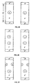
- FIG. 1 is the schematic diagram of a prior art VDMOST, where FIG. 1A shows the structure and FIG. 1B shows the field profile.
- FIG. 2 shows a voltage sustaining layer structure of this invention, where FIG. 2A shows a voltage sustaining layer structure with islands in one plane.
- FIGS. 2B and 2C show the structures of the voltage sustaining layer with the floating islands in two planes.
- FIG. 3 shows the structure and the field profile of a VDMOST with the voltage sustaining layer of this invention.
- the voltage sustaining layer of FIG. 2A is used.
- the field profile of this structure under a reverse voltage of V B is shown in FIG. 3B .
- FIG. 3C a voltage sustaining layer of FIG. 2C is used.
- FIG. 4 shows the structure of an IGBT with a voltage sustaining layer of this invention.
- a voltage sustaining layer of FIG. 2A is used.
- a voltage sustaining layer of FIG. 2C is used.
- FIG. 5 shows a structure of a RMOST with the voltage sustaining layer of this invention shown in FIG. 2A .
- FIG. 6 shows a structure of a bipolar junction transistor with the voltage sustaining layer of this invention shown in FIG. 2A .
- FIG. 7 shows a structure of a SIT with the voltage sustaining layer of this invention shown in FIG. 2A .
- FIGS. 3-7 the same numeral designates similar parts of a high voltage semiconductor device, where, 1 designates p (or n) island in the voltage sustaining layer; 3 designates n+ (or p+) substrate; 4 designates p (or n) source body; 5 designates n+ (or p+) source; 6 designates p+ (or n+) substrate; 7 designates n (or p) buffer layer; 8 designates p+ (or n+) outer base of BJT; 9 designates p+ (or n+) grid of SIT; and shaded regions designate oxide regions.
- FIG. 2 shows several structures of a voltage sustaining layer according to the invention.
- the horizontal layout of the voltage sustaining layer can be either interdigitated (finger), or hexagonal (cell), or rectangular (cell). In all the figures of schematic cross-sectional view of the structures, only one or two units (fingers or cells) of the voltage sustaining layer are shown.
- the voltage sustaining layer of this invention can be used in many high voltage devices.
- FIG. 3B shows the field profile along a line through a center of islands in the voltage sustaining layer and perpendicular to said planes in FIG. 3A .
- the turn-off process of a resultant device is almost as fast as a conventional VDMOST.
- the turn-on process is like the turn-off process of a conventional IGBT, which consists of a fast stage and a long tail.
- the long tail is due to the p (or n) islands needing to be charged.
- the design references of a voltage sustaining layer of this invention may be calculated according to above formulas for calculating E C and the average dose of the islands in a plane. For example, at first, a value of a desirable breakdown voltage V B is determined, and the value of E C is calculated from the determined E C . Then, from the technology achievable number of sublayers n, the lateral size of a unit and the width of the islands in a plane, the number of impurity atoms in each island is calculated. The calculated values can be used as the reference values for simulation in CAD if more accurate values are needed.
Abstract
A method of manufacturing a semiconductor device includes preparing a semiconductor wafer with a substrate of a first conductivity type and forming a first epitaxial layer of the first conductivity type on the substrate. The first epitaxial layer has a first thickness. The method further includes growing a first oxide layer on the first epitaxial layer, masking the first oxide layer, ion implanting to create at least one embedded region of a second conductivity type in the first epitaxial layer, removing the first oxide layer, and forming a second epitaxial layer of the first conductivity type on the first epitaxial layer. The second epitaxial layer has the first thickness minus a thickness equal to a thickness of the at least one embedded region of the second conductivity type.
Description
This application is a divisional application of U.S. patent application Ser. No. 11/838,522, filed Aug. 14, 2007, now U.S. Pat. No. 7,498,614; which is a continuation of U.S. patent application Ser. No. 11/365,223, filed Mar. 1, 2006, now U.S. Pat. No. 7,271,067; which is a divisional application of U.S. patent application Ser. No. 10/860,435, filed Jun. 3, 2004, now U.S. Pat. No. 7,227,197; which is a divisional application of U.S. patent application Ser. No. 10/382,027, filed Mar. 5, 2003, now U.S. Pat. No. 6,936,867; which is a divisional application of U.S. patent application Ser. No. 08/953,077, filed Oct. 17, 1997, now U.S. Pat. No. 6,635,906; which is a continuation of U.S. patent application Ser. No. 08/598,386, filed Feb. 8, 1996, now abandoned; which is a continuation of U.S. patent application Ser. No. 08/268,339, filed Jun. 30, 1994, now abandoned.
This invention relates to semiconductor high voltage devices, and specifically to semiconductor high voltage devices with a voltage sustaining layer containing floating regions.
It is well-known that in many semiconductor devices, such as VD-MOST and SIT, a high sustaining voltage always accompanies a high specific on-resistance. This is due to the fact that, for a high sustaining voltage, thickness of a voltage sustaining layer should be large and doping concentration of the voltage sustaining layer should be low, so as the peak field does not exceed the critical field for breakdown −EC, which is normally expressed by EC=8.2×10⁵×VB −0.2V/cm for silicon, where VB is the breakdown voltage of the voltage sustaining layer.
In a uniformly doped n-type voltage sustaining layer between p+-region and n+-region, in order to obtain a minimum specific on-resistance at a given breakdown voltage, a doping concentration ND and a thickness W of the voltage sustaining layer are optimized such that a maximum field is at p+-n-junction and its value is equal to EC, a minimum field is at n+-n-junction and equal to EC/3. For a silicon device,
N D=1.9×10¹⁸ ×V B −1.4 cm−3 (1)
W=1.8×10⁻² ×V B −1.2 ÿm −2 (2)
(see, e.g., P. Rossel, Microelectron. Reliab., vol. 24, No. 2, pp 339-366, 1984).
N D=1.9×10¹⁸ ×V B −1.4 cm−3 (1)
W=1.8×10⁻² ×V B −1.2 ÿm −2 (2)
(see, e.g., P. Rossel, Microelectron. Reliab., vol. 24, No. 2, pp 339-366, 1984).
For the VDMOST shown in FIG. 1A , a field profile in the voltage sustaining layer at VB is shown in FIG. 1B , where a slope of the field versus distance is qND/Es, Es is the permittivity of the semiconductor and q is the electron charge. The change of field through the n-region is qND/Es, 2EC/3. The relation between Ron and VB of a n-type voltage sustaining layer is then expressed by
R on =W/qÿÿ n N D=0.83×10⁻⁸ ×V B 2.5 ÿ.cm2 (3)
where ÿn is the mobility of the electron and ÿn=710×VB 0.1 cm/V.sec is used for silicon.
R on =W/qÿÿ n N D=0.83×10⁻⁸ ×V B 2.5 ÿ.cm2 (3)
where ÿn is the mobility of the electron and ÿn=710×VB 0.1 cm/V.sec is used for silicon.
In order to get even lower Ron at a given VB, some research has been done to optimize the doping profile instead of using a uniform doping, see: [1] C. Hu, IEEE Trans. Electron Devices, vol. ED-2, No. 3, p 243 (1979); [2] V. A. K. Temple et al., IEEE Trans. Electron Devices, vol. ED-27, No. 2, p 243 (1980); [3] X. B. Chen, C. Hu, IEEE Trans. Electron Devices, vol. ED-27, No. 6, p 985-987 (1982). However, the results show no significant improvement.
The purpose of this invention is to provide a semiconductor high voltage device having a new voltage sustaining layer with better relationship between Ron and VB. To achieve the above purpose, a semiconductor high voltage device is provided, which comprises a substrate of a first conductivity type, at least one region of a second conductivity type, and a voltage sustaining layer of the first conductivity type having a plurality of discrete floating (embedded) islands of a second conductivity type between said substrate and said region of the second conductivity type.
According to this invention, an n (or p) type voltage sustaining layer is divided by (n-1) planes into n sub-layers with equal thickness, and p (or n) type discrete floating islands are introduced with their geometrical centers on such planes. The average dose NT of the floating islands in each plane is about 2EsEc/3q. For silicon,
N T=2E s E c/3q=3.53×1012 V B −0.2 cm−2 (4)
N T=2E s E c/3q=3.53×1012 V B −0.2 cm−2 (4)
With such a floating island, the field is reduced by an amount about 2EC/3 from a maximum value EC at a side of the floating island to a minimum value EC/3 at another side of the floating island so far as the floating island is fully depleted. Each sub-layer is designed to sustain a voltage of VB1=VB/n, and to have a thickness and doping concentration which are almost the same as those form formulas (1) and (2) with VB is replaced by VB1, so that when a reverse voltage which is about the breakdown voltage VB is applied over the whole voltage sustaining layer, the maximum field is EC and the minimum field is EC/3, where the locations of the maximum field are not only at the p+-n (or n+-p) junction, but also at the points of each p (or n) island nearest to the n+-n (or p+-p) junction; the locations of the minimum field are not only at the n+-n (or p+-p) junction, but also at the points of each p (or n) islands nearest to the p+-n (or n+-p) junction. An example of the structure of a VDMOST using a voltage sustaining layer of this invention with n=2 is shown in FIG. 3A and the field profile under a reverse voltage of VB is shown in FIG. 3B . Apparently, in such a condition, VB=2WEC/3, where W is the total thickness of the voltage sustaining layer.
It is easy to prove that the above structured voltage sustaining layer including a plurality of floating regions is fully depleted under a reverse bias voltage about VB/2. The flux due to the charges of the ionized donors (or acceptors) under the p (or n) islands are almost totally terminated by the charges of the p (or n) islands. The maximum field is then 2EC/3 and the minimum field is zero, the locations of the maximum field are the same as those under a reverse bias voltage of VB.
Apparently, the p (or n) islands make the field not to be accumulated throughout the whole voltage sustaining layer. For a given value of breakdown voltage VB, the doping concentration ND can be higher than that in a conventional voltage sustaining layer and the specific on-resistance is much lower than that in a conventional voltage sustaining layer.
Suppose that there are n sub-layers in a voltage sustaining layer. Then, each sub-layer can sustain a voltage of VB/n, where VB is the breakdown voltage of the total voltage sustaining layer. Obviously, instead of (3), the relation of Ron and VB of this invention is
Compared to formula (3), it can been seen that the on-resistance of a voltage sustaining layer having n sub-layers is much lower than that of a conventional one.
The inventor has experimented and obtained remarkable results, which show that the on-resistance of a semiconductor device using a voltage sustaining layer with n=2 of this invention is at least lower than ½ of that of a conventional one with the same breakdown voltage, although the real value of Ron of a voltage sustaining layer having floating islands is a little higher than the value calculated from expression (5) when n<3, due to the effect that the current path is narrowed by the p-type floating islands. Besides, for minimizing Ron, the optimum value of NT is slightly different with the expression (4), due to that the negative charges of p-type floating islands are concentrated in the p-regions instead of being uniformly distributed on a plane, whereas these negative charges are used to absorb the flux of ionized donors below that plane.
The foregoing summary, as well as the following detailed description of the invention, will be better understood when read in conjunction with the appended drawings. For the purpose of illustrating the invention, there are shown in the drawings embodiments which are presently preferred. It should be understood, however, that the invention is not limited to the precise arrangements and instrumentalities shown. In the drawings:
All the structures schematically shown in the figures are of cross-sectional view. In FIGS. 3-7 , the same numeral designates similar parts of a high voltage semiconductor device, where, 1 designates p (or n) island in the voltage sustaining layer; 3 designates n+ (or p+) substrate; 4 designates p (or n) source body; 5 designates n+ (or p+) source; 6 designates p+ (or n+) substrate; 7 designates n (or p) buffer layer; 8 designates p+ (or n+) outer base of BJT; 9 designates p+ (or n+) grid of SIT; and shaded regions designate oxide regions.
In FIG. 2A , a voltage sustaining layer with p (or n) islands in a plane is shown (i.e., n=2, two sub-layers). In FIG. 2B , a voltage sustaining layer with p (or n) islands disposed in two planes is shown (i.e., n=3, three sub-layers), where each island in the upper plane is vertically arranged over a corresponding island in the lower plane. FIG. 2C shows another voltage sustaining layer with two planes of p (or n) islands (n=3), wherein each of the islands in the upper plane is vertically arranged in the middle of two neighboring islands in the lower plane.
The horizontal layout of the voltage sustaining layer can be either interdigitated (finger), or hexagonal (cell), or rectangular (cell). In all the figures of schematic cross-sectional view of the structures, only one or two units (fingers or cells) of the voltage sustaining layer are shown.
The voltage sustaining layer of this invention can be used in many high voltage devices.
-
- 1) High voltage diode
This can be simply realized by forming two electrodes on the p+-region and the n+-region in any of structures shown in FIG. 2 .
-
- 2) High voltage (or power) VDMOST
The turn-off process of a resultant device is almost as fast as a conventional VDMOST. The turn-on process is like the turn-off process of a conventional IGBT, which consists of a fast stage and a long tail. The long tail is due to the p (or n) islands needing to be charged.
-
- 3) High Voltage (or Power) IGBT
-
- 4) High Voltage (or Power) RMOST
-
- 5) High Voltage (or Power) BJT
-
- 6) High Voltage (or Power) SIT
The design references of a voltage sustaining layer of this invention may be calculated according to above formulas for calculating EC and the average dose of the islands in a plane. For example, at first, a value of a desirable breakdown voltage VB is determined, and the value of EC is calculated from the determined EC. Then, from the technology achievable number of sublayers n, the lateral size of a unit and the width of the islands in a plane, the number of impurity atoms in each island is calculated. The calculated values can be used as the reference values for simulation in CAD if more accurate values are needed.
An example of a process for making a vertical n-IGBT using the voltage sustaining layer of this invention is stated briefly as follows:
-
- First step: preparing a wafer of a p+-substrate having an n+-buffer on it;
- Second step: forming a n-epilayer on said wafer;
- Third step: growing a thin oxide layer on the epilayer and forming openings by photo-lithograph;
- Fourth step: implanting boron through the openings for making p-islands and then removing the oxide layer;
- Fifth step: repeat (n-1) times of second step to fourth step.
- The following steps are all the same as fabricating a conventional IGBT.
Although the invention has been described and illustrated with reference to specific embodiments thereof, it is not intended that the invention be limited to these illustrative embodiments. Those skilled in the art will recognized that modifications and variations can be made without departing from the spirit of the invention. Therefore, it is intended that this invention encompass all such variations and modifications as fall within the scope of the appended claims.
Claims (3)
1. A method of manufacturing a semiconductor device comprising:
preparing a semiconductor wafer with a substrate of a first conductivity type;
forming a first epitaxial layer of the first conductivity type on the substrate, the first epitaxial layer having a first thickness;
growing a first oxide layer on the first epitaxial layer;
masking the first oxide layer;
ion implanting to create at least one first embedded region of a second conductivity type in the first epitaxial layer;
removing the first oxide layer;
forming a second epitaxial layer of the first conductivity type on the first epitaxial layer, the second epitaxial layer having a second thickness that is greater than the first thickness minus a thickness equal to a thickness, in a direction extending away from the substrate, of the at least one first embedded region of the second conductivity type;
growing a second oxide layer on the second epitaxial layer;
masking the second oxide layer;
ion implanting to create at least one second embedded region of a second conductivity type in the second epitaxial layer; and
removing the second oxide layer.
2. The method according to claim 1 , wherein the first conductivity type is one of n-type and p-type and the second conductivity type is the other of n-type and p-type.
3. The method according to claim 1 , wherein the substrate has a first doping concentration and the first epitaxial layer and the second epitaxial layer have a second doping concentration that is different from the first doping concentration.
Priority Applications (2)
| Application Number | Priority Date | Filing Date | Title |
|---|---|---|---|
| US12/355,165 US8071450B2 (en) | 1993-10-29 | 2009-01-16 | Method for forming voltage sustaining layer with opposite-doped islands for semiconductor power devices |
| US13/280,518 US20120040521A1 (en) | 1993-10-29 | 2011-10-25 | Voltage sustaining layer wiht opposite-doped island for seminconductor power devices |
Applications Claiming Priority (11)
| Application Number | Priority Date | Filing Date | Title |
|---|---|---|---|
| CN93115356A CN1035294C (en) | 1993-10-29 | 1993-10-29 | Withstand voltage layer with special shaped doped island for semiconductor device |
| CN93115356 | 1993-10-29 | ||
| CN93115356.5 | 1993-10-29 | ||
| US26833994A | 1994-06-30 | 1994-06-30 | |
| US59838696A | 1996-02-08 | 1996-02-08 | |
| US08/953,077 US6635906B1 (en) | 1993-10-29 | 1997-10-17 | Voltage sustaining layer with opposite-doped islands for semi-conductor power devices |
| US10/382,027 US6936867B2 (en) | 1993-10-29 | 2003-03-05 | Semiconductor high-voltage devices |
| US10/860,435 US7227197B2 (en) | 1993-10-29 | 2004-06-03 | Semiconductor high-voltage devices |
| US11/365,223 US7271067B2 (en) | 1993-10-29 | 2006-03-01 | Voltage sustaining layer with opposite-doped islands for semiconductor power devices |
| US11/838,522 US7498614B2 (en) | 1993-10-29 | 2007-08-14 | Voltage sustaining layer with opposite-doped islands for semiconductor power devices |
| US12/355,165 US8071450B2 (en) | 1993-10-29 | 2009-01-16 | Method for forming voltage sustaining layer with opposite-doped islands for semiconductor power devices |
Related Parent Applications (1)
| Application Number | Title | Priority Date | Filing Date |
|---|---|---|---|
| US11/838,522 Division US7498614B2 (en) | 1993-10-29 | 2007-08-14 | Voltage sustaining layer with opposite-doped islands for semiconductor power devices |
Related Child Applications (1)
| Application Number | Title | Priority Date | Filing Date |
|---|---|---|---|
| US13/280,518 Continuation US20120040521A1 (en) | 1993-10-29 | 2011-10-25 | Voltage sustaining layer wiht opposite-doped island for seminconductor power devices |
Publications (2)
| Publication Number | Publication Date |
|---|---|
| US20090130828A1 US20090130828A1 (en) | 2009-05-21 |
| US8071450B2 true US8071450B2 (en) | 2011-12-06 |
Family
ID=4990982
Family Applications (7)
| Application Number | Title | Priority Date | Filing Date |
|---|---|---|---|
| US08/953,077 Expired - Fee Related US6635906B1 (en) | 1993-10-29 | 1997-10-17 | Voltage sustaining layer with opposite-doped islands for semi-conductor power devices |
| US10/382,027 Expired - Fee Related US6936867B2 (en) | 1993-10-29 | 2003-03-05 | Semiconductor high-voltage devices |
| US10/860,435 Expired - Fee Related US7227197B2 (en) | 1993-10-29 | 2004-06-03 | Semiconductor high-voltage devices |
| US11/365,223 Expired - Fee Related US7271067B2 (en) | 1993-10-29 | 2006-03-01 | Voltage sustaining layer with opposite-doped islands for semiconductor power devices |
| US11/838,522 Expired - Fee Related US7498614B2 (en) | 1993-10-29 | 2007-08-14 | Voltage sustaining layer with opposite-doped islands for semiconductor power devices |
| US12/355,165 Expired - Fee Related US8071450B2 (en) | 1993-10-29 | 2009-01-16 | Method for forming voltage sustaining layer with opposite-doped islands for semiconductor power devices |
| US13/280,518 Abandoned US20120040521A1 (en) | 1993-10-29 | 2011-10-25 | Voltage sustaining layer wiht opposite-doped island for seminconductor power devices |
Family Applications Before (5)
| Application Number | Title | Priority Date | Filing Date |
|---|---|---|---|
| US08/953,077 Expired - Fee Related US6635906B1 (en) | 1993-10-29 | 1997-10-17 | Voltage sustaining layer with opposite-doped islands for semi-conductor power devices |
| US10/382,027 Expired - Fee Related US6936867B2 (en) | 1993-10-29 | 2003-03-05 | Semiconductor high-voltage devices |
| US10/860,435 Expired - Fee Related US7227197B2 (en) | 1993-10-29 | 2004-06-03 | Semiconductor high-voltage devices |
| US11/365,223 Expired - Fee Related US7271067B2 (en) | 1993-10-29 | 2006-03-01 | Voltage sustaining layer with opposite-doped islands for semiconductor power devices |
| US11/838,522 Expired - Fee Related US7498614B2 (en) | 1993-10-29 | 2007-08-14 | Voltage sustaining layer with opposite-doped islands for semiconductor power devices |
Family Applications After (1)
| Application Number | Title | Priority Date | Filing Date |
|---|---|---|---|
| US13/280,518 Abandoned US20120040521A1 (en) | 1993-10-29 | 2011-10-25 | Voltage sustaining layer wiht opposite-doped island for seminconductor power devices |
Country Status (2)
| Country | Link |
|---|---|
| US (7) | US6635906B1 (en) |
| CN (1) | CN1035294C (en) |
Cited By (4)
| Publication number | Priority date | Publication date | Assignee | Title |
|---|---|---|---|---|
| US20110198692A1 (en) * | 2010-02-17 | 2011-08-18 | Yih-Jau Chang | Semiconductor structure and fabrication method thereof |
| US20120217539A1 (en) * | 2011-02-28 | 2012-08-30 | Infineon Technologies Austria Ag | Semiconductor Component with Improved Dynamic Behavior |
| US20130175608A1 (en) * | 2012-01-11 | 2013-07-11 | Tsung-Hsiung LEE | Semiconductor device and fabricating method thereof |
| CN105957887A (en) * | 2012-07-18 | 2016-09-21 | 英飞凌科技股份有限公司 | Method of Manufacturing Semiconductor Devices Using Ion Implantation and semiconductor device |
Families Citing this family (48)
| Publication number | Priority date | Publication date | Assignee | Title |
|---|---|---|---|---|
| CN1035294C (en) * | 1993-10-29 | 1997-06-25 | 电子科技大学 | Withstand voltage layer with special shaped doped island for semiconductor device |
| US6977420B2 (en) * | 1998-09-30 | 2005-12-20 | National Semiconductor Corporation | ESD protection circuit utilizing floating lateral clamp diodes |
| EP1127379B1 (en) * | 1999-08-19 | 2010-06-02 | Infineon Technologies AG | Vertically structured semiconductor power module |
| US6576516B1 (en) * | 2001-12-31 | 2003-06-10 | General Semiconductor, Inc. | High voltage power MOSFET having a voltage sustaining region that includes doped columns formed by trench etching and diffusion from regions of oppositely doped polysilicon |
| KR100767078B1 (en) * | 2003-10-08 | 2007-10-15 | 도요다 지도샤 가부시끼가이샤 | Insulated gate type semiconductor device and manufacturing method thereof |
| WO2005065179A2 (en) | 2003-12-19 | 2005-07-21 | Third Dimension (3D) Semiconductor, Inc. | Method of manufacturing a superjunction device |
| US7023069B2 (en) * | 2003-12-19 | 2006-04-04 | Third Dimension (3D) Semiconductor, Inc. | Method for forming thick dielectric regions using etched trenches |
| KR100879588B1 (en) * | 2003-12-19 | 2009-01-21 | 써드 디멘존 세미컨덕터, 인코포레이티드 | Planarization method of manufacturing a superjunction device |
| JP4999464B2 (en) * | 2003-12-19 | 2012-08-15 | サード ディメンジョン (スリーディ) セミコンダクタ インコーポレイテッド | Method for manufacturing superjunction devices with wide mesas |
| WO2005065140A2 (en) * | 2003-12-19 | 2005-07-21 | Third Dimension (3D) Semiconductor, Inc. | Method of manufacturing a superjunction device with conventional terminations |
| US7439583B2 (en) * | 2004-12-27 | 2008-10-21 | Third Dimension (3D) Semiconductor, Inc. | Tungsten plug drain extension |
| TWI401749B (en) * | 2004-12-27 | 2013-07-11 | Third Dimension 3D Sc Inc | Process for high voltage superjunction termination |
| CN101189710B (en) * | 2005-04-22 | 2011-05-04 | 艾斯莫斯技术公司 | Superjunction device having oxide lined trenches and method for manufacturing a superjunction device having oxide lined trenches |
| US20070012983A1 (en) * | 2005-07-15 | 2007-01-18 | Yang Robert K | Terminations for semiconductor devices with floating vertical series capacitive structures |
| US7446018B2 (en) | 2005-08-22 | 2008-11-04 | Icemos Technology Corporation | Bonded-wafer superjunction semiconductor device |
| US7723172B2 (en) | 2007-04-23 | 2010-05-25 | Icemos Technology Ltd. | Methods for manufacturing a trench type semiconductor device having a thermally sensitive refill material |
| US8580651B2 (en) * | 2007-04-23 | 2013-11-12 | Icemos Technology Ltd. | Methods for manufacturing a trench type semiconductor device having a thermally sensitive refill material |
| EP2208229A4 (en) | 2007-09-21 | 2011-03-16 | Fairchild Semiconductor | Superjunction structures for power devices and methods of manufacture |
| US8012806B2 (en) | 2007-09-28 | 2011-09-06 | Icemos Technology Ltd. | Multi-directional trenching of a die in manufacturing superjunction devices |
| US7846821B2 (en) * | 2008-02-13 | 2010-12-07 | Icemos Technology Ltd. | Multi-angle rotation for ion implantation of trenches in superjunction devices |
| US8030133B2 (en) | 2008-03-28 | 2011-10-04 | Icemos Technology Ltd. | Method of fabricating a bonded wafer substrate for use in MEMS structures |
| US20120273916A1 (en) | 2011-04-27 | 2012-11-01 | Yedinak Joseph A | Superjunction Structures for Power Devices and Methods of Manufacture |
| JP5271022B2 (en) * | 2008-10-01 | 2013-08-21 | 株式会社豊田中央研究所 | Semiconductor device |
| US8673700B2 (en) | 2011-04-27 | 2014-03-18 | Fairchild Semiconductor Corporation | Superjunction structures for power devices and methods of manufacture |
| US8772868B2 (en) | 2011-04-27 | 2014-07-08 | Fairchild Semiconductor Corporation | Superjunction structures for power devices and methods of manufacture |
| US8786010B2 (en) | 2011-04-27 | 2014-07-22 | Fairchild Semiconductor Corporation | Superjunction structures for power devices and methods of manufacture |
| US8836028B2 (en) | 2011-04-27 | 2014-09-16 | Fairchild Semiconductor Corporation | Superjunction structures for power devices and methods of manufacture |
| CN102420251A (en) * | 2011-12-05 | 2012-04-18 | 电子科技大学 | VDMOS (Vertical Double-Diffusion Metal-Oxide-Semiconductor) device with non-uniform floating island structure |
| US8946814B2 (en) | 2012-04-05 | 2015-02-03 | Icemos Technology Ltd. | Superjunction devices having narrow surface layout of terminal structures, buried contact regions and trench gates |
| CN103151392A (en) * | 2013-02-07 | 2013-06-12 | 电子科技大学 | Vertical gallium nitride-based heterojunction field effect transistor with p type gallium nitride buried layer |
| US9236458B2 (en) * | 2013-07-11 | 2016-01-12 | Infineon Technologies Ag | Bipolar transistor and a method for manufacturing a bipolar transistor |
| CN104810408A (en) * | 2014-01-24 | 2015-07-29 | 无锡华润华晶微电子有限公司 | Super barrier rectifier and manufacturing method thereof |
| US10340885B2 (en) | 2014-05-08 | 2019-07-02 | Avago Technologies International Sales Pte. Limited | Bulk acoustic wave devices with temperature-compensating niobium alloy electrodes |
| CN104167442B (en) * | 2014-08-29 | 2017-04-12 | 电子科技大学 | Vertical GaN heterojunction field-effect transistor with P type GaN island |
| WO2016079846A1 (en) * | 2014-11-20 | 2016-05-26 | 日産自動車株式会社 | Coat drying device and coat drying method |
| CN106298974B (en) * | 2015-05-22 | 2019-07-05 | 朱江 | A kind of semiconductor junction device |
| CN105390536A (en) * | 2015-09-30 | 2016-03-09 | 深圳市可易亚半导体科技有限公司 | Insulated gate bipolar transistor and manufacturing method thereof |
| GB201604796D0 (en) | 2015-11-10 | 2016-05-04 | Analog Devices Global | A combined isolator and power switch |
| US9698594B2 (en) | 2015-11-10 | 2017-07-04 | Analog Devices Global | Overvoltage protection device, and a galvanic isolator in combination with an overvoltage protection device |
| US9653455B1 (en) | 2015-11-10 | 2017-05-16 | Analog Devices Global | FET—bipolar transistor combination |
| US9935628B2 (en) * | 2015-11-10 | 2018-04-03 | Analog Devices Global | FET—bipolar transistor combination, and a switch comprising such a FET—bipolar transistor combination |
| CN105720089B (en) * | 2016-02-16 | 2018-10-26 | 上海华虹宏力半导体制造有限公司 | Super junction and its manufacturing method |
| US9704949B1 (en) * | 2016-06-30 | 2017-07-11 | General Electric Company | Active area designs for charge-balanced diodes |
| CN106340535A (en) * | 2016-08-01 | 2017-01-18 | 苏州捷芯威半导体有限公司 | Semiconductor device and manufacturing method thereof |
| CN110212015A (en) * | 2019-04-30 | 2019-09-06 | 上海功成半导体科技有限公司 | Super junction device structure and preparation method thereof |
| CN110224017A (en) * | 2019-04-30 | 2019-09-10 | 上海功成半导体科技有限公司 | Super junction device structure and preparation method thereof |
| CN111370469A (en) * | 2020-04-30 | 2020-07-03 | 上海华虹宏力半导体制造有限公司 | Super junction device structure and manufacturing method thereof |
| CN114220848B (en) * | 2022-02-22 | 2022-05-10 | 浙江大学 | Floating island device capable of being rapidly opened and manufacturing method thereof |
Citations (23)
| Publication number | Priority date | Publication date | Assignee | Title |
|---|---|---|---|---|
| US3404295A (en) | 1964-11-30 | 1968-10-01 | Motorola Inc | High frequency and voltage transistor with added region for punch-through protection |
| US3497777A (en) | 1967-06-13 | 1970-02-24 | Stanislas Teszner | Multichannel field-effect semi-conductor device |
| US3564356A (en) | 1968-10-24 | 1971-02-16 | Tektronix Inc | High voltage integrated circuit transistor |
| JPS5238889A (en) | 1975-09-22 | 1977-03-25 | Mitsubishi Electric Corp | Vertical junction type field effect transistor |
| US4754310A (en) | 1980-12-10 | 1988-06-28 | U.S. Philips Corp. | High voltage semiconductor device |
| US4775881A (en) | 1984-05-30 | 1988-10-04 | Max-Planck-Gesellschaft Zur Forderung Der Wissenschaften E.V. | Semiconductor device for detecting electromagnetic radiation or particles |
| US4821095A (en) | 1987-03-12 | 1989-04-11 | General Electric Company | Insulated gate semiconductor device with extra short grid and method of fabrication |
| US4868624A (en) | 1980-05-09 | 1989-09-19 | Regents Of The University Of Minnesota | Channel collector transistor |
| US5027180A (en) | 1986-12-11 | 1991-06-25 | Mitsubishi Electric Corporation | Double gate static induction thyristor |
| US5105243A (en) | 1987-02-26 | 1992-04-14 | Kabushiki Kaisha Toshiba | Conductivity-modulation metal oxide field effect transistor with single gate structure |
| US5216275A (en) | 1991-03-19 | 1993-06-01 | University Of Electronic Science And Technology Of China | Semiconductor power devices with alternating conductivity type high-voltage breakdown regions |
| US5218226A (en) | 1989-11-01 | 1993-06-08 | U.S. Philips Corp. | Semiconductor device having high breakdown voltage |
| US5219777A (en) | 1991-06-14 | 1993-06-15 | Gold Star Electron Co., Ltd. | Metal oxide semiconductor field effect transistor and method of making the same |
| US5389815A (en) | 1992-04-28 | 1995-02-14 | Mitsubishi Denki Kabushiki Kaisha | Semiconductor diode with reduced recovery current |
| US5418376A (en) | 1993-03-02 | 1995-05-23 | Toyo Denki Seizo Kabushiki Kaisha | Static induction semiconductor device with a distributed main electrode structure and static induction semiconductor device with a static induction main electrode shorted structure |
| US5430311A (en) | 1991-09-20 | 1995-07-04 | Hitachi, Ltd. | Constant-voltage diode for over-voltage protection |
| US5438215A (en) | 1993-03-25 | 1995-08-01 | Siemens Aktiengesellschaft | Power MOSFET |
| US5510287A (en) | 1994-11-01 | 1996-04-23 | Taiwan Semiconductor Manuf. Company | Method of making vertical channel mask ROM |
| US5519245A (en) | 1989-08-31 | 1996-05-21 | Nippondenso Co., Ltd. | Insulated gate bipolar transistor with reverse conducting current |
| US5572048A (en) | 1992-11-20 | 1996-11-05 | Hitachi, Ltd. | Voltage-driven type semiconductor device |
| US6011298A (en) | 1996-12-31 | 2000-01-04 | Stmicroelectronics, Inc. | High voltage termination with buried field-shaping region |
| US6066878A (en) | 1997-11-10 | 2000-05-23 | Intersil Corporation | High voltage semiconductor structure |
| US6635906B1 (en) | 1993-10-29 | 2003-10-21 | Third Dimension (3D) Semiconductor | Voltage sustaining layer with opposite-doped islands for semi-conductor power devices |
-
1993
- 1993-10-29 CN CN93115356A patent/CN1035294C/en not_active Expired - Lifetime
-
1997
- 1997-10-17 US US08/953,077 patent/US6635906B1/en not_active Expired - Fee Related
-
2003
- 2003-03-05 US US10/382,027 patent/US6936867B2/en not_active Expired - Fee Related
-
2004
- 2004-06-03 US US10/860,435 patent/US7227197B2/en not_active Expired - Fee Related
-
2006
- 2006-03-01 US US11/365,223 patent/US7271067B2/en not_active Expired - Fee Related
-
2007
- 2007-08-14 US US11/838,522 patent/US7498614B2/en not_active Expired - Fee Related
-
2009
- 2009-01-16 US US12/355,165 patent/US8071450B2/en not_active Expired - Fee Related
-
2011
- 2011-10-25 US US13/280,518 patent/US20120040521A1/en not_active Abandoned
Patent Citations (27)
| Publication number | Priority date | Publication date | Assignee | Title |
|---|---|---|---|---|
| US3404295A (en) | 1964-11-30 | 1968-10-01 | Motorola Inc | High frequency and voltage transistor with added region for punch-through protection |
| US3497777A (en) | 1967-06-13 | 1970-02-24 | Stanislas Teszner | Multichannel field-effect semi-conductor device |
| US3564356A (en) | 1968-10-24 | 1971-02-16 | Tektronix Inc | High voltage integrated circuit transistor |
| JPS5238889A (en) | 1975-09-22 | 1977-03-25 | Mitsubishi Electric Corp | Vertical junction type field effect transistor |
| US4868624A (en) | 1980-05-09 | 1989-09-19 | Regents Of The University Of Minnesota | Channel collector transistor |
| US4754310A (en) | 1980-12-10 | 1988-06-28 | U.S. Philips Corp. | High voltage semiconductor device |
| US4775881A (en) | 1984-05-30 | 1988-10-04 | Max-Planck-Gesellschaft Zur Forderung Der Wissenschaften E.V. | Semiconductor device for detecting electromagnetic radiation or particles |
| US5027180A (en) | 1986-12-11 | 1991-06-25 | Mitsubishi Electric Corporation | Double gate static induction thyristor |
| US5105243A (en) | 1987-02-26 | 1992-04-14 | Kabushiki Kaisha Toshiba | Conductivity-modulation metal oxide field effect transistor with single gate structure |
| US4821095A (en) | 1987-03-12 | 1989-04-11 | General Electric Company | Insulated gate semiconductor device with extra short grid and method of fabrication |
| US5519245A (en) | 1989-08-31 | 1996-05-21 | Nippondenso Co., Ltd. | Insulated gate bipolar transistor with reverse conducting current |
| US5218226A (en) | 1989-11-01 | 1993-06-08 | U.S. Philips Corp. | Semiconductor device having high breakdown voltage |
| US5216275A (en) | 1991-03-19 | 1993-06-01 | University Of Electronic Science And Technology Of China | Semiconductor power devices with alternating conductivity type high-voltage breakdown regions |
| US5219777A (en) | 1991-06-14 | 1993-06-15 | Gold Star Electron Co., Ltd. | Metal oxide semiconductor field effect transistor and method of making the same |
| US5430311A (en) | 1991-09-20 | 1995-07-04 | Hitachi, Ltd. | Constant-voltage diode for over-voltage protection |
| US5389815A (en) | 1992-04-28 | 1995-02-14 | Mitsubishi Denki Kabushiki Kaisha | Semiconductor diode with reduced recovery current |
| US5572048A (en) | 1992-11-20 | 1996-11-05 | Hitachi, Ltd. | Voltage-driven type semiconductor device |
| US5418376A (en) | 1993-03-02 | 1995-05-23 | Toyo Denki Seizo Kabushiki Kaisha | Static induction semiconductor device with a distributed main electrode structure and static induction semiconductor device with a static induction main electrode shorted structure |
| US5438215A (en) | 1993-03-25 | 1995-08-01 | Siemens Aktiengesellschaft | Power MOSFET |
| US6635906B1 (en) | 1993-10-29 | 2003-10-21 | Third Dimension (3D) Semiconductor | Voltage sustaining layer with opposite-doped islands for semi-conductor power devices |
| US6936867B2 (en) | 1993-10-29 | 2005-08-30 | Third Dimension Semiconductor, Inc. | Semiconductor high-voltage devices |
| US7227197B2 (en) | 1993-10-29 | 2007-06-05 | Third Dimension (3D) Semiconductor, Inc. | Semiconductor high-voltage devices |
| US7271067B2 (en) | 1993-10-29 | 2007-09-18 | Third Dimension (3D) Semiconductor, Inc. | Voltage sustaining layer with opposite-doped islands for semiconductor power devices |
| US7498614B2 (en) | 1993-10-29 | 2009-03-03 | Third Dimension (3D) Semiconductor, Inc. | Voltage sustaining layer with opposite-doped islands for semiconductor power devices |
| US5510287A (en) | 1994-11-01 | 1996-04-23 | Taiwan Semiconductor Manuf. Company | Method of making vertical channel mask ROM |
| US6011298A (en) | 1996-12-31 | 2000-01-04 | Stmicroelectronics, Inc. | High voltage termination with buried field-shaping region |
| US6066878A (en) | 1997-11-10 | 2000-05-23 | Intersil Corporation | High voltage semiconductor structure |
Non-Patent Citations (13)
| Title |
|---|
| Bai et al., "Junction Termination Technique for Super Junction Devices," Center for Power Electronics Systems (2000). |
| Chenming Hu; Optimum Doping Profile for minimum Ohmic Resistance and High-Breakdown Voltage; IEEE Transactions on Electron Devices, vol. ED-26, No. 3, pp. 243-244; Mar. 1979. |
| Daniel et al., "Modeling of the CoolMOS Transistor-Part I: Device Physics," IEEE Transactions on Electron Devices, vol. 49, No. 5, pp. 916-922 (May 2002). |
| Daniel et al., "Modeling of the CoolMOS Transistor—Part I: Device Physics," IEEE Transactions on Electron Devices, vol. 49, No. 5, pp. 916-922 (May 2002). |
| Daniel et al., "Modeling of the CoolMOS Transistor-Part II: DC Model and Parameter Extraction," IEEE Transactions on Electron Devices, vol. 49, No. 5, pp. 923-929 (May 2002). |
| Daniel et al., "Modeling of the CoolMOS Transistor—Part II: DC Model and Parameter Extraction," IEEE Transactions on Electron Devices, vol. 49, No. 5, pp. 923-929 (May 2002). |
| Fujihira, Tatsuhiko, "Theory of Semiconductor Superjunction Devices," Jpn. J. Appl. Phys., vol. 36, pp. 6254-6262 (1997). |
| Mawby, PA, "MOS Devices," IGDS Course, University of Wales Swansea (2003). |
| P. Rossel; Power M.O.S. Devices; Microelectron, Reliab., vol. 24, No. 2, pp. 359-366; 1984. |
| Saito et al., "600V Semi-superjunction MOSFET," Papers of Technical Meeting on Electron Devices, IEE Japan, vol. Ed. 03, No. 44-49, pp. 27-30 (2003). |
| Victor A.K. Temple et al.; A 600-Volt MOSFET Designed for Low On-Resistance; IEEE Transactions on Electron Devices, vol. ED-27, No. 2, pp. 343-349; Feb. 1980. |
| Xing-Bi Chen et al.; Optimum Doping Profile of Power MOSFET; IEEE Transactions on Electron Devices, vol. ED-29, No. 6, pp. 985-987; Jun. 1982. |
| Yamauchi et al., "Electrical Properties of Super Junction p-n-Diodes Fabricated by Trench Filling," 15th International Symposium on Power Semiconductor Devices and ICs, pp. 207-210 (2003). |
Cited By (8)
| Publication number | Priority date | Publication date | Assignee | Title |
|---|---|---|---|---|
| US20110198692A1 (en) * | 2010-02-17 | 2011-08-18 | Yih-Jau Chang | Semiconductor structure and fabrication method thereof |
| US8154078B2 (en) * | 2010-02-17 | 2012-04-10 | Vanguard International Semiconductor Corporation | Semiconductor structure and fabrication method thereof |
| US20120217539A1 (en) * | 2011-02-28 | 2012-08-30 | Infineon Technologies Austria Ag | Semiconductor Component with Improved Dynamic Behavior |
| US9105682B2 (en) * | 2011-02-28 | 2015-08-11 | Infineon Technologies Austria Ag | Semiconductor component with improved dynamic behavior |
| US20130175608A1 (en) * | 2012-01-11 | 2013-07-11 | Tsung-Hsiung LEE | Semiconductor device and fabricating method thereof |
| US8836017B2 (en) * | 2012-01-11 | 2014-09-16 | Vanguard International Semiconductor Corporation | Semiconductor device and fabricating method thereof |
| CN105957887A (en) * | 2012-07-18 | 2016-09-21 | 英飞凌科技股份有限公司 | Method of Manufacturing Semiconductor Devices Using Ion Implantation and semiconductor device |
| CN105957887B (en) * | 2012-07-18 | 2019-06-18 | 英飞凌科技股份有限公司 | Use the method and semiconductor devices of ion implanting manufacturing semiconductor devices |
Also Published As
| Publication number | Publication date |
|---|---|
| US20070272999A1 (en) | 2007-11-29 |
| US20120040521A1 (en) | 2012-02-16 |
| CN1102274A (en) | 1995-05-03 |
| CN1035294C (en) | 1997-06-25 |
| US20030160281A1 (en) | 2003-08-28 |
| US7498614B2 (en) | 2009-03-03 |
| US6936867B2 (en) | 2005-08-30 |
| US20090130828A1 (en) | 2009-05-21 |
| US20060177995A1 (en) | 2006-08-10 |
| US6635906B1 (en) | 2003-10-21 |
| US7227197B2 (en) | 2007-06-05 |
| US20050035406A1 (en) | 2005-02-17 |
| US7271067B2 (en) | 2007-09-18 |
Similar Documents
| Publication | Publication Date | Title |
|---|---|---|
| US8071450B2 (en) | Method for forming voltage sustaining layer with opposite-doped islands for semiconductor power devices | |
| US6383836B2 (en) | Diode and method for manufacturing the same | |
| US5168331A (en) | Power metal-oxide-semiconductor field effect transistor | |
| US6306728B1 (en) | Stable high voltage semiconductor device structure | |
| JP2988871B2 (en) | Trench gate power MOSFET | |
| EP0115093A2 (en) | Semiconductor devices having increased break-down voltage | |
| US4206469A (en) | Power metal-oxide-semiconductor-field-effect-transistor | |
| EP0103138A2 (en) | Semiconductor rectifier diode | |
| WO1999056323A1 (en) | Semiconductor device and process for manufacturing the same | |
| JPH0888357A (en) | Lateral igbt | |
| US4746967A (en) | Semiconductor device | |
| JPH01149464A (en) | Semiconductor device | |
| KR100194681B1 (en) | Semiconductor structure and manufacturing process with reduced reverse transfer capacitance | |
| JPH11307657A (en) | Semiconductor integrated circuit | |
| RU2006103C1 (en) | Integrated circuit of high-voltage rectifier | |
| JPS5972764A (en) | Semiconductor device | |
| KR19980035251A (en) | Semiconductor device having double epitaxial layer and buried region and manufacturing method thereof |
Legal Events
| Date | Code | Title | Description |
|---|---|---|---|
| REMI | Maintenance fee reminder mailed | ||
| LAPS | Lapse for failure to pay maintenance fees | ||
| STCH | Information on status: patent discontinuation |
Free format text: PATENT EXPIRED DUE TO NONPAYMENT OF MAINTENANCE FEES UNDER 37 CFR 1.362 |
|
| FP | Expired due to failure to pay maintenance fee |
Effective date: 20151206 |