US8076244B2 - Methods for causing fluid to flow through or into via holes, vents and other openings or recesses that communicate with surfaces of substrates of semiconductor device components - Google Patents
Methods for causing fluid to flow through or into via holes, vents and other openings or recesses that communicate with surfaces of substrates of semiconductor device components Download PDFInfo
- Publication number
- US8076244B2 US8076244B2 US11/351,640 US35164006A US8076244B2 US 8076244 B2 US8076244 B2 US 8076244B2 US 35164006 A US35164006 A US 35164006A US 8076244 B2 US8076244 B2 US 8076244B2
- Authority
- US
- United States
- Prior art keywords
- substrate
- chamber
- boundary
- generating
- pressure
- Prior art date
- Legal status (The legal status is an assumption and is not a legal conclusion. Google has not performed a legal analysis and makes no representation as to the accuracy of the status listed.)
- Active, expires
Links
Images


Classifications
-
- H—ELECTRICITY
- H01—ELECTRIC ELEMENTS
- H01L—SEMICONDUCTOR DEVICES NOT COVERED BY CLASS H10
- H01L21/00—Processes or apparatus adapted for the manufacture or treatment of semiconductor or solid state devices or of parts thereof
- H01L21/02—Manufacture or treatment of semiconductor devices or of parts thereof
- H01L21/04—Manufacture or treatment of semiconductor devices or of parts thereof the devices having at least one potential-jump barrier or surface barrier, e.g. PN junction, depletion layer or carrier concentration layer
- H01L21/18—Manufacture or treatment of semiconductor devices or of parts thereof the devices having at least one potential-jump barrier or surface barrier, e.g. PN junction, depletion layer or carrier concentration layer the devices having semiconductor bodies comprising elements of Group IV of the Periodic System or AIIIBV compounds with or without impurities, e.g. doping materials
- H01L21/30—Treatment of semiconductor bodies using processes or apparatus not provided for in groups H01L21/20 - H01L21/26
- H01L21/302—Treatment of semiconductor bodies using processes or apparatus not provided for in groups H01L21/20 - H01L21/26 to change their surface-physical characteristics or shape, e.g. etching, polishing, cutting
- H01L21/306—Chemical or electrical treatment, e.g. electrolytic etching
- H01L21/30604—Chemical etching
-
- H—ELECTRICITY
- H01—ELECTRIC ELEMENTS
- H01L—SEMICONDUCTOR DEVICES NOT COVERED BY CLASS H10
- H01L21/00—Processes or apparatus adapted for the manufacture or treatment of semiconductor or solid state devices or of parts thereof
- H01L21/67—Apparatus specially adapted for handling semiconductor or electric solid state devices during manufacture or treatment thereof; Apparatus specially adapted for handling wafers during manufacture or treatment of semiconductor or electric solid state devices or components ; Apparatus not specifically provided for elsewhere
- H01L21/67005—Apparatus not specifically provided for elsewhere
- H01L21/67011—Apparatus for manufacture or treatment
- H01L21/67017—Apparatus for fluid treatment
- H01L21/67063—Apparatus for fluid treatment for etching
- H01L21/67075—Apparatus for fluid treatment for etching for wet etching
- H01L21/67086—Apparatus for fluid treatment for etching for wet etching with the semiconductor substrates being dipped in baths or vessels
-
- C—CHEMISTRY; METALLURGY
- C09—DYES; PAINTS; POLISHES; NATURAL RESINS; ADHESIVES; COMPOSITIONS NOT OTHERWISE PROVIDED FOR; APPLICATIONS OF MATERIALS NOT OTHERWISE PROVIDED FOR
- C09K—MATERIALS FOR MISCELLANEOUS APPLICATIONS, NOT PROVIDED FOR ELSEWHERE
- C09K13/00—Etching, surface-brightening or pickling compositions
-
- H—ELECTRICITY
- H01—ELECTRIC ELEMENTS
- H01L—SEMICONDUCTOR DEVICES NOT COVERED BY CLASS H10
- H01L21/00—Processes or apparatus adapted for the manufacture or treatment of semiconductor or solid state devices or of parts thereof
- H01L21/67—Apparatus specially adapted for handling semiconductor or electric solid state devices during manufacture or treatment thereof; Apparatus specially adapted for handling wafers during manufacture or treatment of semiconductor or electric solid state devices or components ; Apparatus not specifically provided for elsewhere
- H01L21/67005—Apparatus not specifically provided for elsewhere
- H01L21/67011—Apparatus for manufacture or treatment
- H01L21/67017—Apparatus for fluid treatment
- H01L21/67063—Apparatus for fluid treatment for etching
- H01L21/67075—Apparatus for fluid treatment for etching for wet etching
- H01L21/6708—Apparatus for fluid treatment for etching for wet etching using mainly spraying means, e.g. nozzles
Definitions
- the present invention relates generally to techniques for exposing or applying substrates of semiconductor device components to fluids and, more specifically, to methods in which fluid flows or is forced beyond a feature.
- the present invention relates to etch techniques and, more specifically, to etch methods in which an etchant flows or is forced beyond a feature while etching the feature. More particularly, the present invention relates to methods for forming vent holes of desired dimension in the bottom of so-called “blind ended” via holes.
- the present invention also relates to apparatus for causing an etchant to flow across a feature to be etched.
- via holes through substrates, including semiconductor substrates, such as silicon wafers. Some via holes are formed so as to extend completely through a substrate, while others, which are referred to in the art as “blind ended” via holes, extend only partially through the substrate.
- a blind ended via hole may be formed in the surface of a substrate by a variety of processes, including etch techniques that are timed in such a way as to permit the hole to extend only partially through the thickness of the substrate, which thickness may typically be about about 700 ⁇ m to about 800 ⁇ m in the case of a full-thickness semiconductor wafer.
- a vent which communicates with the via hole, may be formed in the other, opposite surface of the substrate.
- the presence of a vent facilitates the introduction of materials into and the formation of material layers within the relative small (typically about 50 ⁇ m diameter) via hole.
- the size of the vent hole is typically small relative to (e.g., about one tenth of) the size of the blind ended via hole (e.g., about 5 ⁇ m diameter).
- a vent may be formed by directing a laser beam of appropriate wavelength and intensity onto the surface of the substrate opposite the mouth of the via hole at a location that is in alignment with and, thus, opposite from its corresponding via hole.
- a focal point of the laser is positioned at a location just within the bottom of the via hole.
- the laser forms a vent that communicates with the other surface of the substrate, as well as a vent hole that establishes communication between the vent and the blind ended via hole.
- vent or vent hole residual material may collect on the surfaces of a laser drilled features exposed to the heat of the laser (termed the “heat affected zone”), such as the vent or vent hole.
- This residual material is referred to as “slag.”
- the laser may form a vent hole with dimensions that are within reasonable tolerances, the size of the vent hole may be effectively reduced, or even closed, by the slag that results from use of a laser to form the vent and vent hole.
- material deposition may not proceed in a desirable fashion. As a consequence, the resulting via may include undesirable structural defects.
- the present invention includes processes and apparatus for causing, or forcing, an etchant to flow past a feature, such as a surface, from which material is to be removed.
- the material may protrude into, be located along a sidewall of, or obstruct a recess or aperture that extends into a surface of a substrate.
- the present invention includes a method for causing a fluid to flow into or through recesses or apertures, also termed openings, that are formed in or through a substrate. Pressurization of the fluid may cause the fluid to flow into or through the recesses or apertures.
- the fluid may be pressurized by introducing at least a portion of a substrate within a volume of fluid and applying a differential pressure on opposite sides of the substrate. As the differential pressure is applied, the fluid flows or is otherwise forced into or through recesses or apertures, especially those that extend substantially through the substrate.
- the differential pressure may be generated across the substrate by applying a positive pressure or a negative pressure to a fixed volume of fluid on one side of the substrate.
- Application of a positive pressure includes applying a greater amount of pressure to one side of the substrate than is present at the opposite side of the substrate.
- Application of a negative pressure similarly includes application of a lesser pressure to a side of the substrate than is present at the opposite side of the substrate.
- Other nonlimiting examples of the manner in which the fluid may be pressurized include use of a nozzle or other apparatus that directs fluid under pressure toward a surface of a substrate that includes recesses or apertures, as well as movement of a substrate through a volume of fluid in a direction substantially transverse to a plane of the substrate, which movement generates an increased pressure at a leading surface of the substrate.
- a differential pressure may be applied in a substantially continuous, substantially constant manner, applied intermittently in a patterned or random fashion, oscillated, or even alternated, to reverse the direction in which fluid flows into or through openings that extend substantially through a substrate.
- Processes that incorporate teachings of the present invention may be conducted on a single wafer, multiple wafers that are positioned along a single barrier, or multiple wafers that are oriented parallel to one another and arranged in series along a flow path and transverse to the direction thereof.
- the fluid may, by way of example only, comprise an etchant, solvent, or other material that dissolves or is otherwise suitable to remove material.
- a method for altering the internal surfaces of a vent hole, via hole, or other aperture that extends substantially through a substrate includes causing an etchant to flow into or through the apertures.
- Such processes may be used to effect a number of ends, including, without limitation, removal of slag from a vent hole at the bottom of a blind ended via, to smooth the side wall of an aperture that extends substantially through the substrate, modification of the configuration of an aperture that extends substantially through the substrate, or the like.
- the present invention includes apparatus and systems for pressurizing fluid and causing the same to flow into or through recesses or apertures that communicate with a surface of a substrate.
- apparatus and systems include, but are not limited to, differential pressure apparatus in which a substrate is positioned along a boundary between different pressures, apparatus that are configured to pressurize fluid and direct the same toward a surface of a substrate, and apparatus that are configured to carry a substrate through a volume of fluid such that pressure is increased at a leading surface of the substrate.
- FIGS. 1 through 3 depict a substrate that may be processed in accordance with teachings of the present invention to remove obstructions or other irregularities in, or enlarge, apertures that extend through the substrate, with FIG. 1 showing an upper surface of a substrate, FIG. 2 comprising a partial cross-sectional view through a portion of the thickness of the substrate, and FIG. 3 being a representation of a bottom surface, or back side, of the substrate;
- FIG. 4 is a schematic representation of a differential pressure apparatus and method for causing etchant or another fluid to flow through apertures of a substrate;
- FIG. 4A is schematic representation of a variation of the differential pressure apparatus shown in FIG. 4 ;
- FIGS. 5 and 6 illustrate an example of a differential pressure chamber that is configured to hold a substrate at a boundary between regions of different pressure to facilitate flow of fluid through apertures that extend through or substantially through a substrate;
- FIGS. 7 and 8 depict an example of a substrate retainer and corresponding features on a chamber that that may be included in the differential pressure apparatus that incorporates teachings of the present invention
- FIGS. 9 and 10 illustrate another example of retainer and corresponding features of a chamber that may be included in a differential pressure apparatus according to the present invention
- FIGS. 11 and 12 represent another example of retainer and corresponding features of a chamber of a differential pressure apparatus of the present invention
- FIG. 13 depicts use of a positive pressure to cause etchant to flow through an at least partially obstructed aperture of a substrate
- FIG. 14 illustrates use of a negative pressure to cause etchant to flow through an at least partially obstructed aperture of a substrate
- FIGS. 15 through 18 are schematic illustrations of apparatus that may be used to simultaneously cause fluid to flow through apertures of a plurality of substrates
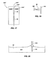
- FIG. 19 is a schematic representation of a system for directing fluid under pressure onto a substrate to cause fluid to flow into or through recesses or apertures that communicate with the surface of the substrate;
- FIG. 20 schematically depicts a system for moving one or more substrates through a volume of fluid to generate an increased pressure at a leading surface of the substrate and, thus, cause the fluid to enter into or flow through recesses or apertures that communicate with that surface of the substrate.
- Substrate 110 may comprise a full or partial semiconductor substrate (e.g., a full or partial wafer of silicon, gallium arsenide, indium phosphide, or another semiconductor material), a silicon-on-insulator (SOI) type substrate (e.g., silicon-on-ceramic (SOC), silicon-on-glass (SOG), silicon-on-sapphire (SOS), etc.), a dielectric substrate (e.g., glass, ceramic, an organic material, etc.), or any other material suitable for use in forming electronic components that form or carry one or more conductive circuits.
- SOI silicon-on-insulator
- SOI silicon-on-insulator
- SOC silicon-on-ceramic
- SOG silicon-on-glass
- SOS silicon-on-sapphire
- dielectric substrate e.g., glass, ceramic, an organic material, etc.
- Apertures 114 may extend partially through a thickness of substrate 110 or, as shown, substantially through a thickness of substrate 110 (e.g., from one major surface 116 thereof to an opposite major surface 122 thereof). Without limiting the scope of the present invention, apertures 114 may comprise vias that extend through substrate 110 .
- one or more apertures 114 may also include a relatively small vent hole 114 b (with a diameter of, e.g., up to about 5 ⁇ m) that is intended to communicate with blind via 114 a and that extends into the opposite major surface 122 of substrate 110 .
- Vias or other apertures 114 may be formed by a variety of known processes, such as by laser drilling processes (e.g., with a laser intermittently pulsed from four or more different angles that converge at a single point). Some processes that are used to form apertures 114 in or through a substrate may result in obstructions 115 (e.g., material slag from melting or obliterating substrate 110 with a laser, etc.) or other irregularities (e.g., surface irregularities, such as roughness, bumps, etc.) within apertures 114 . Thus, following the formation of apertures 114 , they may not be ready or acceptable for subsequent processing.
- obstructions 115 e.g., material slag from melting or obliterating substrate 110 with a laser, etc.
- other irregularities e.g., surface irregularities, such as roughness, bumps, etc.
- FIG. 4 shows a differential pressure apparatus 10 , which, without limiting the scope of the present invention, may be used with a fluid, such as an etchant, solvent, or other suitable liquid (e.g., a suitable surfactant, either separately or in solution with an etchant or solvent, may facilitate wetting of the surfaces of features that are to be removed by the etchant or solvent) to remove obstructions 115 ( FIG. 2 ) or other irregularities from recesses in (including, without limitation, relatively high aspect ratio recesses) or apertures 114 of a substrate 110 , or to change a size, shape, or geometry (e.g., between one or more of cylindrical, hourglass, frustoconical, etc.) of one or more apertures 114 ( FIGS.
- a fluid such as an etchant, solvent, or other suitable liquid (e.g., a suitable surfactant, either separately or in solution with an etchant or solvent, may facilitate wetting of the surfaces of features that are to be removed by the
- Apparatus 10 includes a pressurizable chamber 12 for holding a volume of fluid 50 , such as an etchant, solvent, or other suitable fluid.
- a boundary 15 which may be located somewhat centrally within chamber 12 , separates chamber 12 into an upstream side 12 U and a downstream side 12 D, referring to the direction in which an etchant, solvent, or other suitable fluid moves through chamber 12 when a differential pressure is generated across boundary 15 .
- a substrate holder 16 may be positioned within chamber 12 , along boundary 15 .
- Chamber 12 includes means for facilitating access to an interior thereof of a type known in the art (e.g., an access panel or door, a lid, etc.), which may seal against a remainder of chamber 12 and, thus, facilitate the generation of a non-ambient positive or negative pressure within chamber 12 .
- chamber 12 may have dimensions or features, such as a heater, cooler, or heat transfer mechanism exposed to fluid 50 or through which fluid 50 is circulated, that facilitate maintenance of fluid 50 therein at a desired temperature.
- Substrate holder 16 includes a receptacle 22 for receiving a substrate 110 .
- Receptacle 22 includes a sealing element (not shown) that is configured to prevent fluid 50 from flowing between substrate holder 16 and an outer periphery 112 of substrate 110 as fluid 50 flows through apertures 114 that extend between opposite major surfaces 116 and 122 of substrate 110 ( FIGS. 1 through 3 ).
- FIGS. 5 and 6 show an example of a chamber 12 , chamber 412 , that includes an integral substrate holder 16 .
- Chamber 412 includes two sides 412 a and 412 b , each of which defines a volume 421 a , 421 b .
- Sides 412 a and 412 b are configured to be assembled and sealingly secured together so that a combined volume 421 defined collectively by sides 412 a and 412 b may be pressurized with a positive pressure or a negative pressure.
- Edges 417 a and 417 b of sides 412 a and 412 b are configured to abut one another when sides 412 a and 412 b are properly assembled with each other.
- a ledge 416 a , 416 b may be recessed just beneath each edge 417 a , 417 b , and is configured to support peripheral portions 118 , 124 ( FIGS. 1 through 3 ) of major surfaces 116 , 122 of a substrate 110 , which is held in positioned at a boundary 415 between volume 421 a and 421 b when sides 412 a and 412 b are assembled with each other, with portions of major surfaces 116 and 122 exposed to volumes 421 a and 421 b .
- ledges 416 a and 416 b form a receptacle 22 for a substrate 110 .
- One or both of ledges 416 a and 416 b may form a substantially continuous support for peripheral portions 118 , 124 of a major surface 116 , 122 of substrate 110 .
- a sealing element 424 a , 424 b e.g., an annular gasket, an o-ring, etc.
- a sealing element 424 a , 424 b which may have a somewhat annular shape to facilitate sealing against surface 116 , 122 while exposing at least a portion of surface 116 , 122 through a center thereof, may be positioned on and secured in place (e.g., with adhesive, within a groove 430 , etc.) relative to each ledge 416 a , 416 b.
- FIGS. 7 through 12 A few more, nonlimiting examples of substrate holders 16 , their features, and corresponding features of chambers 12 with which they may be used are illustrated in FIGS. 7 through 12 .
- substrate holder 16 ′ includes a pair of housing elements 16 a ′ and 16 b ′ that, when assembled, are configured to be positioned on opposite sides of substrate 110 (i.e., adjacent to surfaces 116 and 122 ). Interior surfaces 17 a ′ and 17 b ′ of housing elements 16 a ′ and 16 b ′, respectively, are configured to face one another when housing elements 16 a ′ and 16 b ′ are assembled.
- Each housing element 16 a ′, 16 b ′ includes an opening 26 a ′, 26 b ′, which appears as a window, having substantially the same shape as and slightly smaller dimensions (e.g., diameter) than substrate 110 .
- Interior surface 17 a ′, 17 b ′ of one or both housing elements 16 a ′, 16 b ′ may include a recess 28 a ′, 28 b ′ that is located around, or circumscribes, an entire periphery of opening 26 a ′, 26 b ′.
- Recess 28 a ′, 28 b ′ is configured to at least partially receive a peripheral portion 118 , 124 of a major surface 116 , 122 of substrate 110 , and may position substrate 110 at a desired location relative to opening 26 a ′, 26 b ′.
- housing elements 16 a ′ and 16 b ′ and recess 28 a ′, 28 b ′ if any, form a receptacle for substrate 110 .
- sealing element 24 a ′, 24 b ′ is associated with recess 28 a ′, 28 b ′ to seal against substrate 110 , at or near outer periphery 112 thereof.
- sealing element 24 a ′, 24 b ′ may comprise a ring of compliant material (e.g., silicone or another elastomer), which may be seated within a groove (not shown) formed in recess 28 a ′, 28 b ′ or otherwise secured in place relative to recess 28 a ′, 28 b ′.
- compliant material e.g., silicone or another elastomer
- Sealing element 24 a ′, 24 b ′ may be sized and configured for placement against a major surface 116 , 122 of substrate 110 , near outer periphery 112 thereof (i.e., against peripheral portion 118 , 124 ), as shown, or for placement against outer periphery 112 or a corner 120 , 126 formed at the junction between a major surface 116 , 122 and outer periphery 112 .
- an assembled, secured substrate holder 16 ′ includes an outer edge 32 ′, which may be received within a groove 34 ′ formed in chamber 12 ′ to define a boundary within chamber 12 ′.
- Groove 34 ′ may extend completely around an interior surface of chamber 12 ′.
- a sealing element 38 ′ may be located within groove 34 ′ (e.g., within a subgroove (not shown), within a base 36 ′ of groove 34 ′, etc.) and configured to seal against outer edge 32 ′ of substrate holder 16 ′.
- substrate holder 16 ′′ which is fixed within or comprises an integral part of chamber 12 ′′, defines a sealable boundary 15 ′′ between an upstream side 12 U′′ and a downstream side 12 D′′ of chamber 12 ′′.
- Substrate holder 16 ′′ includes a fixed element 16 a ′′, which extends along boundary 15 ′′ inwardly from portions of an interior surface of chamber 12 ′′ that define the entire outer periphery of boundary 15 ′′.
- An opening 26 a ′′ which has dimensions that facilitate exposure of a substantial portion (e.g., substantially all, device or interposer bearing regions, etc.) of substrate 110 without exposing outer periphery 112 of substrate 110 is located centrally or somewhat centrally through fixed element 16 a ′′.
- a recess 28 a ′′ may circumscribe an entire periphery 27 a ′′ of opening 26 a ′′ within a substrate-carrying surface 17 a ′′ of fixed element 16 a ′′.
- Recess 28 a ′′ may be configured to at least partially receive a peripheral portion 118 , 124 ( FIGS. 1 through 3 ) of a major surface 116 , 122 of substrate 110 and, optionally, to position substrate 110 at a desired location relative to opening 26 a ′′.
- substrate-carrying surface 17 a ′′ of fixed element 16 a ′′ may face upstream side 12 U′′ of chamber 12 ′′.
- substrate-carrying surface 17 a ′′ and recess 28 a ′′, if any, serve as a receptacle for substrate 110 .
- a sealing element 24 a ′′ which is configured to abut and seal against substrate 110 may be carried by and, optionally, secured to substrate-carrying surface 17 a ′′ of fixed element 16 a ′′, around periphery 27 a ′′ of the opening 26 a ′′ therethrough.
- sealing element 24 a ′′ may be held within a groove (not shown) that circumscribes periphery 27 a ′′ of opening 26 a ′′ or otherwise be secured to substrate-carrying surface 17 a ′′.
- substrate holder 16 ′′ may include a retainer 16 b ′′ positionable over a substrate 110 that has been assembled with fixed element 16 a ′′.
- Retainer 16 b ′′ has smaller dimensions than fixed element 16 a ′′ to facilitate positioning of retainer 16 b ′′ over, as well as its removal from, fixed element 16 a ′′.
- Retainer 16 b ′′ includes an opening 26 b ′′ that is configured to substantially align with opening 26 a ′′ of fixed element 16 ′′ and to expose a substantial portion of a major surface 116 , 122 of substrate 110 .
- retainer 16 b ′′ may include a recess 28 b ′′ on a substrate-facing surface 17 b ′′ thereof, which surface is also configured to face substrate-carrying surface 17 a ′′ of fixed element 16 a ′′ as retainer 16 b ′′ is positioned over, assembled with, and secured to fixed element 16 a ′′.
- recess 28 b ′′ may be configured to receive a peripheral portion 118 , 124 ( FIGS. 1 and 3 ) of a major surface 116 , 122 of substrate 110 and, optionally, to position substrate 110 at a desired location relative to opening 26 b ′′.
- a sealing element, cushion, or other gasket may be associated with substrate-facing surface 17 b ′′ of retainer 16 b ′′ to establish a seal against or protect a major surface 116 , 122 of substrate 110 as retainer 16 b ′′ is positioned over substrate 110 .
- Retainer 16 b ′′ may be secured to fixed element 16 a ′′ by any suitable means for engagement 60 ′′ within the abilities of one of skill in the art (e.g., one or more clamping elements on fixed element 16 a ′′ that engage edges of retainer 16 b ′′; features that facilitate rotatable engagement between fixed element 16 a ′′ and retainer 16 b ′′, such as corresponding tabs and slots or complementary threads, etc.).
- any suitable means for engagement 60 ′′ within the abilities of one of skill in the art (e.g., one or more clamping elements on fixed element 16 a ′′ that engage edges of retainer 16 b ′′; features that facilitate rotatable engagement between fixed element 16 a ′′ and retainer 16 b ′′, such as corresponding tabs and slots or complementary threads, etc.).
- FIGS. 11 and 12 another example of substrate holder 16 ′′′ and a portion of the chamber within which it resides are depicted.
- Opposed, parallel sides 16 a ′′′ and 16 b ′′′ of a base 16 B′′′ of substrate holder 16 ′′′ are arranged so as to define a narrow slot 25 B′′′, or receptacle, within which a substrate 110 may be disposed.
- a ledge 28 B′′′ extending between sides 16 a ′′′ and 16 b ′′′ of base 16 B′′′ is configured to support substrate 110 and to align the same between opposed openings 26 a ′′′ and 26 b ′′′ of sides 16 a ′′′ and 16 b ′′′, respectively.
- a sealing element 24 B′′′ may be positioned on and, optionally, secured to ledge 28 B′′′ so as to form a seal against an outer periphery of substrate 110 that has been inserted into slot 25 B′′′ as sufficient pressure is applied to substrate 110 (e.g., by a snug fit between outer periphery 112 ( FIGS. 1 and 3 ) of substrate 110 and sealing element 24 B′′′, by placing a load on substrate 110 along a vector that creates a seal between outer periphery 112 thereof and sealing element 24 B′′′, or by a combination of the foregoing).
- base 16 B′′′ of substrate holder 16 ′′′ may be configured such that, when a substrate 110 that has been inserted into slot 25 B′′′, a portion of substrate 110 protrudes from or is otherwise exposed beyond base 16 B′′′ (e.g., a major surface 116 , 122 thereof through opening 26 b ′′′, a portion of outer periphery 112 thereof, etc.) to facilitate removal of substrate 110 from slot 25 B′′′ (e.g., with edge-engaging apparatus, as known in the art; with surface-engaging apparatus, as known in the art; manually, etc.).
- substrate holder 16 ′′′ may include an engagement element 16 E′′′, which may be fixed to an inner surface of a chamber (not shown) or may be separate from the inner surface and configured to sealingly engage the same.
- Engagement element 16 E′′′ is configured to be assembled with and to releasably engage base 16 B′′′ of substrate holder 16 ′′′.
- an engagement element 16 E′′′ that is integral with or fixed relative to the inner surface of the chamber may be assembled with base 16 B′′′ when the chamber is closed and sealed.
- assembly may occur before the chamber with which substrate holder 16 ′′′ is configured to be used is closed and sealed. Thereafter, the inner surface of the chamber may seal against engagement element 16 E′′′ as the chamber is closed and sealed.
- engagement element 16 E′′′ includes opposed, parallel sides 16 c ′′′ and 16 d ′′′, which define a narrow slot 25 E′′′ therebetween.
- Sides 16 c ′′′ and 16 d ′′′ and slot 25 E′′′ of engagement element 16 E′′′ are respectively configured to align with sides 16 a ′′′ and 16 b ′′′ and slot 25 B′′′ of base 16 B′′′ when base 16 B′′′ is assembled with engagement element 16 E′′′.
- slot 25 E′′′ may receive a substrate 110 that has been positioned within slot 25 B′′′ of base 16 B′′′ as engagement element 16 E′′′ is aligned, if necessary, and assembled with base 16 B′′′.
- slots 25 B′′′ and 25 E′′′ together form a receptacle 22 ′′′ for substrate 110 .
- engagement element 16 E′′′ also includes a ledge 28 E′′′ between sides 16 c ′′′ and 16 d ′′′.
- Ledge 28 E′′′ carries a sealing element 24 E′′′ that is configured to abut a portion of outer periphery 112 of substrate 110 that is not engaged by sealing element 24 B′′′ of base 16 B′′′ when engagement element 16 E′′′ is assembled with a substrate 110 -carrying base 16 B′′′.
- base 16 B′′′ and engagement element 16 E′′′ of substrate holder 16 ′′′ may be mechanically associated with one another in any suitable manner that is within the skill of one in the art (e.g., with a simple hinge that establishes a clam-shell type relationship between base 16 B′′′ and engagement element 16 E′′′, a more complex mechanism that automatically aligns engagement element 16 E′′′ over base 16 B′′′ as these elements are assembled and, optionally, maintains the assembled relationship between these elements, etc.).
- Engagement element 16 E′′′ may optionally include at least one engagement feature 60 E′′′ which is configured to engage a corresponding engagement feature 60 B′′′ of base 16 B′′′ and, thus, to maintain the assembled relationship between base 16 B′′′ and engagement/release element 16 E′′′ of substrate holder 16 ′′′.
- differential pressure apparatus various embodiments of differential pressure apparatus, chambers 12 and substrate holders 16 will be apparent to those of ordinary skill in the art.
- An optional inlet 18 may communicate with upstream side 12 U of chamber 12 to allow fluid 50 to flow therein or therefrom, while an optional outlet 20 may communicate with downstream side 12 D of chamber 12 to allow fluid 50 to flow therein or therefrom.
- inlet 18 and outlet 20 may be coupled to a pump 40 , which generates a differential pressure across boundary 15 of chamber 12 and, thus, across substrate 110 by simultaneously drawing fluid 50 from one side 12 U, 12 D of chamber 12 and pumping fluid 50 into the other side 12 D, 12 U of chamber 12 .
- inlet 18 and/or outlet 20 may communicate with one or more reservoirs or fluid sources to facilitate the introduction of different types of fluids within at least a portion of chamber 12 at a particular point during processing of a substrate 110 .
- a pressurization component may be associated with (e.g., communicate with) one or both of upstream side 12 U and downstream side 12 D of chamber 12 .
- a source 42 of positive pressure may be associated with upstream side 12 U or a source 44 of negative pressure may be associated with downstream side 12 D.
- either source 42 or 44 may be configured to selectively increase or decrease pressure within a corresponding side 12 U, 12 D of chamber 12 .
- Either source 42 , 44 may be configured to change the pressure in the side 12 U, 12 D of chamber 12 with which it is associated by changing the amount of fluid within that side 12 U, 12 D of chamber 12 .
- source 42 may create a relatively higher pressure within upstream side 12 U by introducing a fluid, such as fluid 50 , or another fluid (e.g., gas, liquid, etc.) that is inert or compatible with fluid 50 without displacing a significant portion of fluid 50 from upstream side 12 U.
- source 44 may create a relatively lower pressure within downstream side 12 D of chamber 12 by removing fluid 50 or gas from downstream side 12 D.
- Various types of pumps and associated motors may be used as source 42 or source 44 , as known in the art.
- differential pressure apparatus 10 including means for controlling a temperature of fluid 50 (as an other-than-ambient temperature may be required or desirable for the desired processing; e.g., silicon etchants are more effective at elevated temperatures, etc.), means for introducing substrate holder 16 into chamber 12 , means for operating substrate holder 16 , means for handling substrates 110 , means for closing and sealing chamber 12 , means for introducing fluid 50 into chamber 12 and removing fluid 50 from chamber 12 , and the like, will be apparent to and understood by one of skill in the art.
- a temperature of fluid 50 as an other-than-ambient temperature may be required or desirable for the desired processing; e.g., silicon etchants are more effective at elevated temperatures, etc.
- substrate holder 16 when a substrate 110 has been placed within substrate holder 16 , substrate holder 16 or a portion thereof has been sealed against an inner surface of chamber 12 , if necessary, and chamber 12 is sealed, substrate holder 16 and substrate 110 together form a physical boundary, which is positioned along boundary 15 , that facilitates the generation of a differential pressure within chamber 12 (i.e., a different amount of pressure within upstream side 12 U from that within downstream side 12 D).
- FIGS. 13 and 14 provide two examples of the manner in which a pressure differential may be applied, or generated, across substrate 110 .
- a pressure differential may be generated by applying a positive pressure to upstream side 12 U of chamber 12 .
- the amount of positive pressure applied exceeds an ambient pressure within downstream side 12 D of chamber 12 .
- Positive pressure may be applied, by a pump 40 or other pressure source (e.g., source 42 shown in FIG. 4A ) that communicates with upstream side 12 U of chamber, by introducing a fluid (e.g., gas, liquid, such as additional fluid, etc.) into the sealed upstream side 12 U of chamber 12 without displacing any of the fluid previously present within upstream side 12 U.
- a fluid e.g., gas, liquid, such as additional fluid, etc.
- the presence of greater pressure on upstream side 12 U than downstream side 12 D causes fluid 50 from upstream side 12 U to enter into recesses or apertures 114 ( FIGS.
- any obstructions 115 FIG. 2
- other irregularities e.g., bumps, protrusions, surface roughness, etc.
- the flow of fluid 50 past obstructions 115 or any other irregularities may expedite the removal process.
- pressure within downstream side 12 D of chamber 12 may be decreased.
- fluid e.g., gas, such as air, liquid, such as fluid 50 , etc.
- FIGS. 1 through 3 the fluid that has been removed from downstream side 12 D.
- downstream side 12 D The lesser pressure on downstream side 12 D than upstream side 12 U causes fluid 50 to be drawn from upstream side 12 U, into apertures 114 of substrate 110 , which is located at the boundary 15 between a relatively high pressure and a relatively low pressure, and into downstream side 12 D. As fluid 50 flows into and through apertures 114 , desired processing may be effected.
- a differential pressure may be applied in a substantially continuous, substantially constant manner, applied intermittently in a patterned or random fashion, oscillated, or even alternated, to reverse the direction in which etchant flows into or through recess or apertures 114 that extend substantially through a substrate 110 (see FIGS. 1 through 3 ).
- the difference in pressure across a boundary 15 may correspond to the rate at which fluid 50 flows through apertures 114 ( FIGS. 1 through 3 ) and, thus, the amount of fluid 50 that flows past an obstruction 115 or other irregularity over a given period of time, the difference in pressure may also correspond to the rate at which material is removed from apertures 114 or surfaces thereof.
- differential pressure apparatus configured to hold and process a single substrate 110 at a time
- differential pressure apparatus configured to hold and process two or more substrates 10 simultaneously are also within the scope of the present invention, as shown in FIGS. 15 through 17 .
- FIG. 15 depicts a differential pressure apparatus 210 that includes a chamber 212 with a frame 213 that is positioned along a boundary 215 that surrounds a centrally or somewhat centrally located portion 212 a of chamber 212 and separates the same from a peripherally located portion 212 b of chamber 212 .
- Frame 213 is configured to carry a plurality of substrate holders 16 .
- substrate holders 16 are assembled with frame 213 , if necessary, and chamber 212 is sealed, frame 213 , substrate holders 16 , and substrates 110 collectively isolate portion 212 a from portion 212 b in such a way that a differential pressure may be generated across boundary 215 .
- this configuration of differential pressure apparatus 210 positions substrates 110 along a single boundary, it may be said that differential pressure apparatus 210 positions substrates 110 “in parallel” to one other, whether or not substrates 110 are actually oriented parallel to each other.
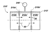
- FIG. 16 illustrates a differential pressure apparatus 210 ′ that includes a pressurizable chamber 212 ′ with two spaced apart boundaries 215 a ′ and 215 b ′ therein. Boundaries 215 a ′ and 215 b ′ define a central region 212 a ′ between two outer regions 212 b ′.
- a substrate holder 16 that carries a substrate 110 may be positioned substantially along each boundary 215 a ′, 215 b ′ to facilitate the generation of a differential pressure, in parallel, across each boundary 215 a ′, 215 b ′.
- One or more pressurization components 240 ′ may be associated with chamber 212 ′ in such a way as to vary a pressure in central region 212 a ′ relative to the pressure with each outer region 212 b ′. If, for example, a relatively lower pressure is generated within central region 212 a ′, fluid 50 may be drawn from outer regions 212 b ′, through apertures 114 ( FIGS. 1 through 3 ) in substrates 110 , and into central region 212 b ′. Alternatively, if a relatively higher pressure is generated within central region 212 a ′ than the pressure present within outer regions 212 b ′, fluid 50 may be forced from central region 212 a ′, through apertures 114 , and into outer regions 212 b′.
- differential pressure apparatus 210 ′′ is configured similarly to differential pressure apparatus 10 , but includes a frame 213 ′′, which carries two or more substrate holders 16 , positionable substantially along a boundary 215 ′′ of a pressurizable chamber 212 ′′ to separate and upstream side 212 U′′ of chamber 212 ′′ from a downstream side 212 D′′ thereof.
- Differential pressure apparatus 210 ′′′ includes plural substrate holders 16 that are oriented “in series.” As a substrate 110 is assembled with each substrate holder 16 , chamber 212 ′′′ is sealed, and different regions 212 a ′′′, 212 b ′′′, 212 c ′′′, etc., are substantially isolated from one another, a pressure differential may be generated from a region 212 a ′′′ at a first end of chamber 212 ′′′ and a region 212 c ′′′ at an opposite end of chamber 212 ′′′. As in the previously described embodiments of differential pressure apparatus, the pressure differential causes fluid 50 to be forced or drawn into or through apertures 114 ( FIGS. 1 through 3 ) in substrates 110 .
- differential pressure apparatus that are configured to position at least one substrate 110 in parallel with at least one other substrate 110 and in series with still another substrate 110 are also within the scope of the present invention.
- fluid 50 under pressure may be directed toward a surface 116 , 122 of substrate 110 and into apertures 114 ( FIGS. 1 through 3 ) or recesses that communicate with surface 116 , 122 .
- a substrate holder 316 may carry one or more substrates 110 through a volume 312 of fluid 50 , generating an increase in pressure across a leading surface 116 , 122 ( FIGS.
- teachings of the present invention are not limited to use with fluids 50 that are configured to remove obstructions 115 or other irregularities from apertures 114 or recesses in a substrate 110 .
- teachings thereof may also be used to cause fluids that react with material at the surfaces of apertures 114 or recesses or that deposit or coat materials onto the surfaces of apertures 114 or recesses to flow into or through apertures 114 or recesses of a substrate 110 .
Abstract
Description
Claims (39)
Priority Applications (3)
| Application Number | Priority Date | Filing Date | Title |
|---|---|---|---|
| US11/351,640 US8076244B2 (en) | 2006-02-10 | 2006-02-10 | Methods for causing fluid to flow through or into via holes, vents and other openings or recesses that communicate with surfaces of substrates of semiconductor device components |
| US13/306,122 US8956498B2 (en) | 2006-02-10 | 2011-11-29 | Apparatuses facilitating fluid flow into via holes, vents, and other openings communicating with surfaces of substrates of semiconductor device components |
| US14/607,945 US20150140817A1 (en) | 2006-02-10 | 2015-01-28 | Apparatuses facilitating fluid flow into via holes, vents, and other openings communicating with surfaces of substrates of semiconductor device components |
Applications Claiming Priority (1)
| Application Number | Priority Date | Filing Date | Title |
|---|---|---|---|
| US11/351,640 US8076244B2 (en) | 2006-02-10 | 2006-02-10 | Methods for causing fluid to flow through or into via holes, vents and other openings or recesses that communicate with surfaces of substrates of semiconductor device components |
Related Child Applications (1)
| Application Number | Title | Priority Date | Filing Date |
|---|---|---|---|
| US13/306,122 Division US8956498B2 (en) | 2006-02-10 | 2011-11-29 | Apparatuses facilitating fluid flow into via holes, vents, and other openings communicating with surfaces of substrates of semiconductor device components |
Publications (2)
| Publication Number | Publication Date |
|---|---|
| US20070190785A1 US20070190785A1 (en) | 2007-08-16 |
| US8076244B2 true US8076244B2 (en) | 2011-12-13 |
Family
ID=38369174
Family Applications (3)
| Application Number | Title | Priority Date | Filing Date |
|---|---|---|---|
| US11/351,640 Active 2028-10-31 US8076244B2 (en) | 2006-02-10 | 2006-02-10 | Methods for causing fluid to flow through or into via holes, vents and other openings or recesses that communicate with surfaces of substrates of semiconductor device components |
| US13/306,122 Active 2026-11-29 US8956498B2 (en) | 2006-02-10 | 2011-11-29 | Apparatuses facilitating fluid flow into via holes, vents, and other openings communicating with surfaces of substrates of semiconductor device components |
| US14/607,945 Abandoned US20150140817A1 (en) | 2006-02-10 | 2015-01-28 | Apparatuses facilitating fluid flow into via holes, vents, and other openings communicating with surfaces of substrates of semiconductor device components |
Family Applications After (2)
| Application Number | Title | Priority Date | Filing Date |
|---|---|---|---|
| US13/306,122 Active 2026-11-29 US8956498B2 (en) | 2006-02-10 | 2011-11-29 | Apparatuses facilitating fluid flow into via holes, vents, and other openings communicating with surfaces of substrates of semiconductor device components |
| US14/607,945 Abandoned US20150140817A1 (en) | 2006-02-10 | 2015-01-28 | Apparatuses facilitating fluid flow into via holes, vents, and other openings communicating with surfaces of substrates of semiconductor device components |
Country Status (1)
| Country | Link |
|---|---|
| US (3) | US8076244B2 (en) |
Cited By (1)
| Publication number | Priority date | Publication date | Assignee | Title |
|---|---|---|---|---|
| US20170028692A1 (en) * | 2015-07-30 | 2017-02-02 | Korea Institute Of Science And Technology | Apparatus and method for graphene wet transfer |
Families Citing this family (5)
| Publication number | Priority date | Publication date | Assignee | Title |
|---|---|---|---|---|
| US7494925B2 (en) * | 2004-02-23 | 2009-02-24 | Micron Technology, Inc. | Method for making through-hole conductors for semiconductor substrates |
| US8076244B2 (en) | 2006-02-10 | 2011-12-13 | Micron Technology, Inc. | Methods for causing fluid to flow through or into via holes, vents and other openings or recesses that communicate with surfaces of substrates of semiconductor device components |
| US9113570B2 (en) * | 2012-10-31 | 2015-08-18 | Tyco Electronics Services Gmbh | Planar electronic device having a magnetic component |
| JP5950855B2 (en) * | 2013-03-19 | 2016-07-13 | 住友重機械イオンテクノロジー株式会社 | Ion implantation apparatus and cleaning method of ion implantation apparatus |
| JP6850986B2 (en) * | 2016-03-28 | 2021-03-31 | 三菱マテリアル株式会社 | Electrode plate cleaning equipment and manufacturing method for plasma processing equipment |
Citations (17)
| Publication number | Priority date | Publication date | Assignee | Title |
|---|---|---|---|---|
| US3158499A (en) | 1961-07-07 | 1964-11-24 | Union Carbide Corp | Method of depositing metal coatings in holes, tubes, cracks, fissures and the like |
| US3886053A (en) | 1973-11-01 | 1975-05-27 | James M Leland | Programmable pulse electroplating process |
| US4396467A (en) | 1980-10-27 | 1983-08-02 | General Electric Company | Periodic reverse current pulsing to form uniformly sized feed through conductors |
| US5166097A (en) | 1990-11-26 | 1992-11-24 | The Boeing Company | Silicon wafers containing conductive feedthroughs |
| US6190834B1 (en) | 1997-05-15 | 2001-02-20 | Hitachi, Ltd. | Photosensitive resin composition, and multilayer printed circuit board using the same |
| US6221769B1 (en) | 1999-03-05 | 2001-04-24 | International Business Machines Corporation | Method for integrated circuit power and electrical connections via through-wafer interconnects |
| US6261407B1 (en) * | 1999-06-29 | 2001-07-17 | Lam Research Corporation | Method and apparatus for removal of thin films from wafers |
| US20020057099A1 (en) | 2000-11-13 | 2002-05-16 | Masayoshi Esashi | Contactor, method for manufacturing the same, and probe card using the same |
| US6410976B1 (en) | 1997-08-22 | 2002-06-25 | Micron Technology, Inc. | Integrated circuitry having conductive passageway interconnecting circuitry on front and back surfaces of a wafer fragment |
| US6458696B1 (en) | 2001-04-11 | 2002-10-01 | Agere Systems Guardian Corp | Plated through hole interconnections |
| US6479382B1 (en) | 2001-03-08 | 2002-11-12 | National Semiconductor Corporation | Dual-sided semiconductor chip and method for forming the chip with a conductive path through the chip that connects elements on each side of the chip |
| US20030116176A1 (en) * | 2001-04-18 | 2003-06-26 | Rothman Laura B. | Supercritical fluid processes with megasonics |
| US20040089557A1 (en) | 2001-11-07 | 2004-05-13 | Shipley Company, L.L.C. | Process for electrolytic copper plating |
| US20050186791A1 (en) | 2004-02-23 | 2005-08-25 | Hiatt William M. | Through-hole conductors for semiconductor substrates and method and system for making same |
| US20060130762A1 (en) * | 2004-12-17 | 2006-06-22 | Lam Research Corp. | Wafer heating and temperature control by backside fluid injection |
| US20080035475A1 (en) | 2004-03-19 | 2008-02-14 | Faraday Technology, Inc. | Electroplating cell with hydrodynamics facilitating more uniform deposition on a workpiece with through holes during plating |
| US7392815B2 (en) * | 2003-03-31 | 2008-07-01 | Lam Research Corporation | Chamber for wafer cleaning and method for making the same |
Family Cites Families (24)
| Publication number | Priority date | Publication date | Assignee | Title |
|---|---|---|---|---|
| US4547836A (en) | 1984-02-01 | 1985-10-15 | General Electric Company | Insulating glass body with electrical feedthroughs and method of preparation |
| US4857716A (en) * | 1986-05-12 | 1989-08-15 | Clinicom Incorporated | Patient identification and verification system and method |
| US5153827A (en) * | 1989-01-30 | 1992-10-06 | Omni-Flow, Inc. | An infusion management and pumping system having an alarm handling system |
| US5594786A (en) * | 1990-07-27 | 1997-01-14 | Executone Information Systems, Inc. | Patient care and communication system |
| US5487218A (en) | 1994-11-21 | 1996-01-30 | International Business Machines Corporation | Method for making printed circuit boards with selectivity filled plated through holes |
| US5781442A (en) * | 1995-05-15 | 1998-07-14 | Alaris Medical Systems, Inc. | System and method for collecting data and managing patient care |
| US6671563B1 (en) * | 1995-05-15 | 2003-12-30 | Alaris Medical Systems, Inc. | System and method for collecting data and managing patient care |
| JP3376258B2 (en) * | 1996-11-28 | 2003-02-10 | キヤノン株式会社 | Anodizing apparatus and related apparatus and method |
| US6222006B1 (en) | 1997-08-13 | 2001-04-24 | Fort James Corporation | Wet strength thermosetting resin formulations and polyaminamide polymers suitable for use in the manufacture of paper products |
| US6090474A (en) | 1998-09-01 | 2000-07-18 | International Business Machines Corporation | Flowable compositions and use in filling vias and plated through-holes |
| US6262003B1 (en) | 1999-05-21 | 2001-07-17 | Colgate- Palmolive Company | Light duty liquid cleaning compositions comprise an alpha hydroxy fatty acid |
| EP2111087B1 (en) | 1999-08-06 | 2011-01-19 | Ibiden Co., Ltd. | Multilayer printed wiring board |
| US6519569B1 (en) * | 1999-12-01 | 2003-02-11 | B. Braun Medical, Inc. | Security infusion pump with bar code reader |
| US6790198B1 (en) * | 1999-12-01 | 2004-09-14 | B-Braun Medical, Inc. | Patient medication IV delivery pump with wireless communication to a hospital information management system |
| JP2001264198A (en) | 2000-03-16 | 2001-09-26 | Olympus Optical Co Ltd | Method for manufacturing multiaxial tactile sensor and tactile sensor |
| US7012008B1 (en) | 2000-03-17 | 2006-03-14 | Advanced Micro Devices, Inc. | Dual spacer process for non-volatile memory devices |
| US6673195B2 (en) * | 2001-03-30 | 2004-01-06 | Industrial Technologies Research Institute | Apparatus and method for etching glass panels |
| JP4392168B2 (en) | 2001-05-09 | 2009-12-24 | 荏原ユージライト株式会社 | Copper plating bath and substrate plating method using the same |
| US6985870B2 (en) * | 2002-01-11 | 2006-01-10 | Baxter International Inc. | Medication delivery system |
| US7810513B1 (en) * | 2002-09-30 | 2010-10-12 | Lam Research Corporation | Substrate preparation using megasonic coupling fluid meniscus and methods, apparatus, and systems for implementing the same |
| JP2004203128A (en) | 2002-12-24 | 2004-07-22 | Sumitomo Rubber Ind Ltd | Pneumatic tire and its manufacturing method |
| DE602004032435D1 (en) * | 2003-06-13 | 2011-06-09 | Sophia Wen | DEVICE FOR THE CHEMICAL TREATMENT OF THIN LAYERS OF SEMICONDUCTORS |
| US20070256710A1 (en) * | 2004-06-10 | 2007-11-08 | Dtl Technologies, Inc. | Chemical process operations on wafers having through-holes and a pressure differential between the major surfaces thereof |
| US8076244B2 (en) * | 2006-02-10 | 2011-12-13 | Micron Technology, Inc. | Methods for causing fluid to flow through or into via holes, vents and other openings or recesses that communicate with surfaces of substrates of semiconductor device components |
-
2006
- 2006-02-10 US US11/351,640 patent/US8076244B2/en active Active
-
2011
- 2011-11-29 US US13/306,122 patent/US8956498B2/en active Active
-
2015
- 2015-01-28 US US14/607,945 patent/US20150140817A1/en not_active Abandoned
Patent Citations (21)
| Publication number | Priority date | Publication date | Assignee | Title |
|---|---|---|---|---|
| US3158499A (en) | 1961-07-07 | 1964-11-24 | Union Carbide Corp | Method of depositing metal coatings in holes, tubes, cracks, fissures and the like |
| US3886053A (en) | 1973-11-01 | 1975-05-27 | James M Leland | Programmable pulse electroplating process |
| US4396467A (en) | 1980-10-27 | 1983-08-02 | General Electric Company | Periodic reverse current pulsing to form uniformly sized feed through conductors |
| US5166097A (en) | 1990-11-26 | 1992-11-24 | The Boeing Company | Silicon wafers containing conductive feedthroughs |
| US6190834B1 (en) | 1997-05-15 | 2001-02-20 | Hitachi, Ltd. | Photosensitive resin composition, and multilayer printed circuit board using the same |
| US6410976B1 (en) | 1997-08-22 | 2002-06-25 | Micron Technology, Inc. | Integrated circuitry having conductive passageway interconnecting circuitry on front and back surfaces of a wafer fragment |
| US6221769B1 (en) | 1999-03-05 | 2001-04-24 | International Business Machines Corporation | Method for integrated circuit power and electrical connections via through-wafer interconnects |
| US6261407B1 (en) * | 1999-06-29 | 2001-07-17 | Lam Research Corporation | Method and apparatus for removal of thin films from wafers |
| US20020057099A1 (en) | 2000-11-13 | 2002-05-16 | Masayoshi Esashi | Contactor, method for manufacturing the same, and probe card using the same |
| US6747465B2 (en) | 2000-11-13 | 2004-06-08 | Tokyo Electron Limited | Contractor, method for manufacturing the same, and probe card using the same |
| US6479382B1 (en) | 2001-03-08 | 2002-11-12 | National Semiconductor Corporation | Dual-sided semiconductor chip and method for forming the chip with a conductive path through the chip that connects elements on each side of the chip |
| US6458696B1 (en) | 2001-04-11 | 2002-10-01 | Agere Systems Guardian Corp | Plated through hole interconnections |
| US20030116176A1 (en) * | 2001-04-18 | 2003-06-26 | Rothman Laura B. | Supercritical fluid processes with megasonics |
| US20040089557A1 (en) | 2001-11-07 | 2004-05-13 | Shipley Company, L.L.C. | Process for electrolytic copper plating |
| US7392815B2 (en) * | 2003-03-31 | 2008-07-01 | Lam Research Corporation | Chamber for wafer cleaning and method for making the same |
| US20050186791A1 (en) | 2004-02-23 | 2005-08-25 | Hiatt William M. | Through-hole conductors for semiconductor substrates and method and system for making same |
| US20060037864A1 (en) | 2004-02-23 | 2006-02-23 | Hiatt William M | Through-hole conductors for semiconductor substrates and system for making same |
| US20060040494A1 (en) | 2004-02-23 | 2006-02-23 | Hiatt William M | Through-hole conductors for semiconductor substrates and method for making same |
| US7396447B2 (en) | 2004-02-23 | 2008-07-08 | Micron Technology, Inc. | Through-hole conductors for semiconductor substrates and system for making same |
| US20080035475A1 (en) | 2004-03-19 | 2008-02-14 | Faraday Technology, Inc. | Electroplating cell with hydrodynamics facilitating more uniform deposition on a workpiece with through holes during plating |
| US20060130762A1 (en) * | 2004-12-17 | 2006-06-22 | Lam Research Corp. | Wafer heating and temperature control by backside fluid injection |
Non-Patent Citations (2)
| Title |
|---|
| Van Zant, "Photolithography-Developing to Final Inspection", Chapter Nine, pp. 226-233, Microchip Fabrication-A Practical Guide to Semiconductor Processing, Second Edition, 1990. |
| Van Zant, "Photolithography-Developing to Final Inspection", Chapter Nine, pp. 226-233, Microchip Fabrication—A Practical Guide to Semiconductor Processing, Second Edition, 1990. |
Cited By (2)
| Publication number | Priority date | Publication date | Assignee | Title |
|---|---|---|---|---|
| US20170028692A1 (en) * | 2015-07-30 | 2017-02-02 | Korea Institute Of Science And Technology | Apparatus and method for graphene wet transfer |
| US9994007B2 (en) * | 2015-07-30 | 2018-06-12 | Korea Institute Of Science And Technology | Apparatus for graphene wet transfer |
Also Published As
| Publication number | Publication date |
|---|---|
| US20120070988A1 (en) | 2012-03-22 |
| US20070190785A1 (en) | 2007-08-16 |
| US20150140817A1 (en) | 2015-05-21 |
| US8956498B2 (en) | 2015-02-17 |
Similar Documents
| Publication | Publication Date | Title |
|---|---|---|
| US20150140817A1 (en) | Apparatuses facilitating fluid flow into via holes, vents, and other openings communicating with surfaces of substrates of semiconductor device components | |
| TWI681440B (en) | Substrate processing apparatus and substrate processing method | |
| JP4410119B2 (en) | Cleaning device, coating, developing device and cleaning method | |
| KR101933077B1 (en) | Focus ring and substrate processing apparatus having same | |
| US7300526B2 (en) | Method and system for removal of contaminates from phaseshift photomasks | |
| JP6802667B2 (en) | Heat treatment equipment, substrate processing equipment, heat treatment method and substrate processing method | |
| CN111180357A (en) | Substrate processing apparatus | |
| US11562968B2 (en) | Apparatus for lithographically forming wafer identification marks and alignment marks | |
| US7357115B2 (en) | Wafer clamping apparatus and method for operating the same | |
| WO2015107950A1 (en) | Substrate processing device and substrate processing method | |
| US10453719B2 (en) | Plasma etching method | |
| US10766054B2 (en) | Substrate processing method and substrate processing apparatus | |
| US20110303642A1 (en) | Substrate processing system, substrate processing method, and storage medium | |
| KR101399904B1 (en) | Apparatus for cleaning substrate with plasma | |
| US11934103B2 (en) | Apparatus for post exposure bake of photoresist | |
| KR102387542B1 (en) | Air supply system and apparatus for treating substrate | |
| KR20110028541A (en) | Chamber and associated methods for wafer processing | |
| KR102139020B1 (en) | Substrate processing apparatus and substrate processing method | |
| KR101927696B1 (en) | Apparatus and method for treating substrate | |
| US7434590B2 (en) | Method and apparatus for clamping a substrate in a high pressure processing system | |
| KR102099267B1 (en) | Apparatus for cleaning and drying substrate | |
| US20220102215A1 (en) | Wafer processing method | |
| US20210035767A1 (en) | Methods for repairing a recess of a chamber component | |
| KR200161684Y1 (en) | Cooling apparatus of wafer used in manufacturing semiconductor | |
| KR20060124314A (en) | Bevel etching process apparatus with multi-paths for fume exhaust |
Legal Events
| Date | Code | Title | Description |
|---|---|---|---|
| AS | Assignment |
Owner name: MICRON TECHNOLOGY, INC., IDAHO Free format text: ASSIGNMENT OF ASSIGNORS INTEREST;ASSIGNOR:DANDO, ROSS S.;REEL/FRAME:017572/0944 Effective date: 20060130 |
|
| FEPP | Fee payment procedure |
Free format text: PAYOR NUMBER ASSIGNED (ORIGINAL EVENT CODE: ASPN); ENTITY STATUS OF PATENT OWNER: LARGE ENTITY |
|
| STCF | Information on status: patent grant |
Free format text: PATENTED CASE |
|
| CC | Certificate of correction | ||
| FPAY | Fee payment |
Year of fee payment: 4 |
|
| AS | Assignment |
Owner name: U.S. BANK NATIONAL ASSOCIATION, AS COLLATERAL AGENT, CALIFORNIA Free format text: SECURITY INTEREST;ASSIGNOR:MICRON TECHNOLOGY, INC.;REEL/FRAME:038669/0001 Effective date: 20160426 Owner name: U.S. BANK NATIONAL ASSOCIATION, AS COLLATERAL AGEN Free format text: SECURITY INTEREST;ASSIGNOR:MICRON TECHNOLOGY, INC.;REEL/FRAME:038669/0001 Effective date: 20160426 |
|
| AS | Assignment |
Owner name: MORGAN STANLEY SENIOR FUNDING, INC., AS COLLATERAL AGENT, MARYLAND Free format text: PATENT SECURITY AGREEMENT;ASSIGNOR:MICRON TECHNOLOGY, INC.;REEL/FRAME:038954/0001 Effective date: 20160426 Owner name: MORGAN STANLEY SENIOR FUNDING, INC., AS COLLATERAL Free format text: PATENT SECURITY AGREEMENT;ASSIGNOR:MICRON TECHNOLOGY, INC.;REEL/FRAME:038954/0001 Effective date: 20160426 |
|
| AS | Assignment |
Owner name: U.S. BANK NATIONAL ASSOCIATION, AS COLLATERAL AGENT, CALIFORNIA Free format text: CORRECTIVE ASSIGNMENT TO CORRECT THE REPLACE ERRONEOUSLY FILED PATENT #7358718 WITH THE CORRECT PATENT #7358178 PREVIOUSLY RECORDED ON REEL 038669 FRAME 0001. ASSIGNOR(S) HEREBY CONFIRMS THE SECURITY INTEREST;ASSIGNOR:MICRON TECHNOLOGY, INC.;REEL/FRAME:043079/0001 Effective date: 20160426 Owner name: U.S. BANK NATIONAL ASSOCIATION, AS COLLATERAL AGEN Free format text: CORRECTIVE ASSIGNMENT TO CORRECT THE REPLACE ERRONEOUSLY FILED PATENT #7358718 WITH THE CORRECT PATENT #7358178 PREVIOUSLY RECORDED ON REEL 038669 FRAME 0001. ASSIGNOR(S) HEREBY CONFIRMS THE SECURITY INTEREST;ASSIGNOR:MICRON TECHNOLOGY, INC.;REEL/FRAME:043079/0001 Effective date: 20160426 |
|
| AS | Assignment |
Owner name: JPMORGAN CHASE BANK, N.A., AS COLLATERAL AGENT, ILLINOIS Free format text: SECURITY INTEREST;ASSIGNORS:MICRON TECHNOLOGY, INC.;MICRON SEMICONDUCTOR PRODUCTS, INC.;REEL/FRAME:047540/0001 Effective date: 20180703 Owner name: JPMORGAN CHASE BANK, N.A., AS COLLATERAL AGENT, IL Free format text: SECURITY INTEREST;ASSIGNORS:MICRON TECHNOLOGY, INC.;MICRON SEMICONDUCTOR PRODUCTS, INC.;REEL/FRAME:047540/0001 Effective date: 20180703 |
|
| AS | Assignment |
Owner name: MICRON TECHNOLOGY, INC., IDAHO Free format text: RELEASE BY SECURED PARTY;ASSIGNOR:U.S. BANK NATIONAL ASSOCIATION, AS COLLATERAL AGENT;REEL/FRAME:047243/0001 Effective date: 20180629 |
|
| MAFP | Maintenance fee payment |
Free format text: PAYMENT OF MAINTENANCE FEE, 8TH YEAR, LARGE ENTITY (ORIGINAL EVENT CODE: M1552); ENTITY STATUS OF PATENT OWNER: LARGE ENTITY Year of fee payment: 8 |
|
| AS | Assignment |
Owner name: MICRON TECHNOLOGY, INC., IDAHO Free format text: RELEASE BY SECURED PARTY;ASSIGNOR:MORGAN STANLEY SENIOR FUNDING, INC., AS COLLATERAL AGENT;REEL/FRAME:050937/0001 Effective date: 20190731 |
|
| AS | Assignment |
Owner name: MICRON SEMICONDUCTOR PRODUCTS, INC., IDAHO Free format text: RELEASE BY SECURED PARTY;ASSIGNOR:JPMORGAN CHASE BANK, N.A., AS COLLATERAL AGENT;REEL/FRAME:051028/0001 Effective date: 20190731 Owner name: MICRON TECHNOLOGY, INC., IDAHO Free format text: RELEASE BY SECURED PARTY;ASSIGNOR:JPMORGAN CHASE BANK, N.A., AS COLLATERAL AGENT;REEL/FRAME:051028/0001 Effective date: 20190731 |
|
| MAFP | Maintenance fee payment |
Free format text: PAYMENT OF MAINTENANCE FEE, 12TH YEAR, LARGE ENTITY (ORIGINAL EVENT CODE: M1553); ENTITY STATUS OF PATENT OWNER: LARGE ENTITY Year of fee payment: 12 |