US8080464B2 - Methods for processing silicon on insulator wafers - Google Patents
Methods for processing silicon on insulator wafers Download PDFInfo
- Publication number
- US8080464B2 US8080464B2 US12/971,788 US97178810A US8080464B2 US 8080464 B2 US8080464 B2 US 8080464B2 US 97178810 A US97178810 A US 97178810A US 8080464 B2 US8080464 B2 US 8080464B2
- Authority
- US
- United States
- Prior art keywords
- wafer
- reactor
- silicon
- temperature
- cleaved surface
- Prior art date
- Legal status (The legal status is an assumption and is not a legal conclusion. Google has not performed a legal analysis and makes no representation as to the accuracy of the status listed.)
- Active
Links
Images


Classifications
-
- H—ELECTRICITY
- H01—ELECTRIC ELEMENTS
- H01L—SEMICONDUCTOR DEVICES NOT COVERED BY CLASS H10
- H01L21/00—Processes or apparatus adapted for the manufacture or treatment of semiconductor or solid state devices or of parts thereof
- H01L21/70—Manufacture or treatment of devices consisting of a plurality of solid state components formed in or on a common substrate or of parts thereof; Manufacture of integrated circuit devices or of parts thereof
- H01L21/71—Manufacture of specific parts of devices defined in group H01L21/70
- H01L21/76—Making of isolation regions between components
- H01L21/762—Dielectric regions, e.g. EPIC dielectric isolation, LOCOS; Trench refilling techniques, SOI technology, use of channel stoppers
- H01L21/7624—Dielectric regions, e.g. EPIC dielectric isolation, LOCOS; Trench refilling techniques, SOI technology, use of channel stoppers using semiconductor on insulator [SOI] technology
-
- H—ELECTRICITY
- H01—ELECTRIC ELEMENTS
- H01L—SEMICONDUCTOR DEVICES NOT COVERED BY CLASS H10
- H01L21/00—Processes or apparatus adapted for the manufacture or treatment of semiconductor or solid state devices or of parts thereof
- H01L21/02—Manufacture or treatment of semiconductor devices or of parts thereof
- H01L21/02104—Forming layers
- H01L21/02365—Forming inorganic semiconducting materials on a substrate
- H01L21/02367—Substrates
- H01L21/0237—Materials
- H01L21/02373—Group 14 semiconducting materials
- H01L21/02381—Silicon, silicon germanium, germanium
-
- H—ELECTRICITY
- H01—ELECTRIC ELEMENTS
- H01L—SEMICONDUCTOR DEVICES NOT COVERED BY CLASS H10
- H01L21/00—Processes or apparatus adapted for the manufacture or treatment of semiconductor or solid state devices or of parts thereof
- H01L21/02—Manufacture or treatment of semiconductor devices or of parts thereof
- H01L21/02104—Forming layers
- H01L21/02365—Forming inorganic semiconducting materials on a substrate
- H01L21/02518—Deposited layers
- H01L21/02521—Materials
- H01L21/02524—Group 14 semiconducting materials
- H01L21/02532—Silicon, silicon germanium, germanium
-
- H—ELECTRICITY
- H01—ELECTRIC ELEMENTS
- H01L—SEMICONDUCTOR DEVICES NOT COVERED BY CLASS H10
- H01L21/00—Processes or apparatus adapted for the manufacture or treatment of semiconductor or solid state devices or of parts thereof
- H01L21/02—Manufacture or treatment of semiconductor devices or of parts thereof
- H01L21/02104—Forming layers
- H01L21/02365—Forming inorganic semiconducting materials on a substrate
- H01L21/02612—Formation types
- H01L21/02617—Deposition types
- H01L21/0262—Reduction or decomposition of gaseous compounds, e.g. CVD
-
- H—ELECTRICITY
- H01—ELECTRIC ELEMENTS
- H01L—SEMICONDUCTOR DEVICES NOT COVERED BY CLASS H10
- H01L21/00—Processes or apparatus adapted for the manufacture or treatment of semiconductor or solid state devices or of parts thereof
- H01L21/02—Manufacture or treatment of semiconductor devices or of parts thereof
- H01L21/02104—Forming layers
- H01L21/02365—Forming inorganic semiconducting materials on a substrate
- H01L21/02656—Special treatments
- H01L21/02658—Pretreatments
-
- H—ELECTRICITY
- H01—ELECTRIC ELEMENTS
- H01L—SEMICONDUCTOR DEVICES NOT COVERED BY CLASS H10
- H01L21/00—Processes or apparatus adapted for the manufacture or treatment of semiconductor or solid state devices or of parts thereof
- H01L21/70—Manufacture or treatment of devices consisting of a plurality of solid state components formed in or on a common substrate or of parts thereof; Manufacture of integrated circuit devices or of parts thereof
- H01L21/77—Manufacture or treatment of devices consisting of a plurality of solid state components or integrated circuits formed in, or on, a common substrate
- H01L21/78—Manufacture or treatment of devices consisting of a plurality of solid state components or integrated circuits formed in, or on, a common substrate with subsequent division of the substrate into plural individual devices
- H01L21/82—Manufacture or treatment of devices consisting of a plurality of solid state components or integrated circuits formed in, or on, a common substrate with subsequent division of the substrate into plural individual devices to produce devices, e.g. integrated circuits, each consisting of a plurality of components
- H01L21/84—Manufacture or treatment of devices consisting of a plurality of solid state components or integrated circuits formed in, or on, a common substrate with subsequent division of the substrate into plural individual devices to produce devices, e.g. integrated circuits, each consisting of a plurality of components the substrate being other than a semiconductor body, e.g. being an insulating body
Definitions
- Semiconductor wafers are generally prepared from a single crystal ingot (e.g., a silicon ingot) which is then sliced into individual wafers. While reference will be made herein to semiconductor wafers constructed from silicon, other materials may be used as well, such as germanium or gallium arsenide.
- One type of wafer is a silicon-on-insulator (SOI) wafer.
- An SOI wafer includes a thin layer of silicon atop an insulating layer (i.e., an oxide layer) which is in turn disposed on a silicon substrate.
- a silicon-on-insulator wafer is a type of silicon-on-insulator structure.
- An example process of making an SOI wafer includes depositing a layer of oxide on a polished front surface of a donor wafer.
- Particles e.g., hydrogen atoms or a combination of hydrogen and helium atoms
- the implanted particles form a cleave plane in the donor wafer at the specified depth at which they were implanted.
- the surface of the donor wafer is cleaned to remove material deposited on the wafer during the implantation process.
- the front surface of the donor wafer is then bonded to a handle wafer to form a bonded wafer.
- the donor wafer and handle wafer are bonded together by exposing the surfaces of the wafers to a plasma containing, for example, oxygen or nitrogen. Exposure to the plasma modifies the structure of the surfaces in a process often referred to as surface activation.
- the wafers are then pressed together and a bond is formed therebetween. This bond is relatively weak, and must be strengthened before further processing can occur.
- the bond between the donor wafer and handle wafer is strengthened by heating or annealing the bonded wafer pair at temperatures between approximately 300° C. and 500° C.
- the elevated temperatures cause the formation of covalent bonds between the adjoining surfaces of the donor wafer and the handle wafer, thus solidifying the bond between the donor wafer and the handle wafer.
- the particles earlier implanted in the donor wafer weaken the cleave plane.
- a portion of the donor wafer is then separated (i.e., cleaved) along the cleave plane from the bonded wafer to form the SOI wafer.
- the bonded wafer is first placed in a fixture in which mechanical force is applied perpendicular to the opposing sides of the bonded wafer in order to pull a portion of the donor wafer apart from the bonded wafer.
- suction cups are used to apply the mechanical force.
- the separation of the portion of the donor wafer is initiated by applying a mechanical wedge at the edge of the bonded wafer at the cleave plane in order to initiate propagation of a crack along the cleave plane.
- the mechanical force applied by the suction cups then pulls the portion of the donor wafer from the bonded wafer, thus forming an SOI wafer.
- the bonded pair may instead be subjected to an elevated temperature over a period of time to separate the portion of the donor wafer from the bonded wafer. Exposure to the elevated temperature causes initiation and propagation of a crack along the cleave plane, thus separating a portion of the donor wafer.
- the resulting SOI wafer comprises a thin layer of silicon (the portion of the donor wafer remaining after cleaving) disposed atop the oxide layer and the handle wafer.
- the cleaved surface of the thin layer of silicon has a rough surface that is ill-suited for end-use applications.
- the damage to the surface may be the result of the particle implantation and the resultant dislocations in the crystal structure of the silicon. Accordingly, additional processing is required to smooth the cleaved surface.
- previous processes used high-temperature gaseous etching (i.e., epitaxial-smoothing (epi-smoothing)) or the deposition of a thin layer of silicon on the surface layer (i.e., epitaxial-deposition (epi-deposition)).
- the etching or deposition is carried out at temperatures where the reaction is transport limited (i.e., the rate of reaction is limited by the availability of fresh reactants).
- These transport limited reactions result in thickness variations (e.g., sharp gradients in the thickness profile) at the edges of the surface layer of silicon. Further processing is needed to eliminate the thickness variations caused by the previous processes.
- One aspect is a method for processing a silicon-on-insulator structure comprising a handle wafer, a silicon layer, and a dielectric layer between the handle wafer and the silicon layer.
- the silicon layer has a cleaved surface defining an outer surface of the structure.
- the method includes inserting the structure into a reactor.
- the cleaved surface of the wafer is then etched while controlling a temperature of the reactor such that the etching reaction is kinetically limited.
- An epitaxial layer is then deposited on the wafer while controlling the temperature of the reactor such that a rate of deposition on the cleaved surface is kinetically limited.
- Another aspect is a method for processing a silicon-on-insulator structure comprising a handle wafer, a silicon layer, and a dielectric layer between the handle wafer and the silicon layer.
- the silicon layer has a cleaved surface defining an outer surface of the structure.
- the method includes inserting the structure into a reactor. The temperature of the reactor is then set such that a rate of etching of the cleaved surface will be kinetically limited. A flow of gaseous etchant is then initiated into the reactor and the cleaved surface is etched.
- Still another aspect is a method for processing a silicon-on-insulator structure comprising a handle wafer, a silicon layer, and a dielectric layer between the handle wafer and the silicon layer.
- the silicon layer has a cleaved surface defining an outer surface of the structure.
- the method includes inserting the structure into a reactor. A temperature of the reactor is then set such that a rate of deposition of silicon on the cleaved surface will be kinetically limited. A flow of deposition gas is then initiated into the reactor and silicon is deposited onto the cleaved surface of the structure.
- FIG. 1A is a top plan view of a donor silicon wafer
- FIG. 1B is a cross-sectional view of the donor silicon wafer of FIG. 1B ;
- FIG. 2 is a cross-sectional view of the donor silicon wafer undergoing ion implantation
- FIG. 3 is a cross-sectional view of a bonded wafer comprising the donor silicon wafer bonded to a handle silicon wafer;
- FIG. 4 is a cross-sectional view of the bonded wafer of FIG. 3 after a portion of the donor wafer has been removed;
- FIG. 5 is a cross-sectional view of the bonded wafer of FIG. 4 after processing of a cleaved surface of the bonded wafer;
- FIG. 6 is an enlarged portion of FIG. 5 with features exaggerated for ease of illustration;
- FIG. 7 is a flow diagram showing a method of performing an epitaxial smoothing process on an SOI wafer
- FIG. 8 is a flow diagram showing a method of performing an epitaxial deposition process on an SOI wafer
- FIG. 9 is a chart showing the relationship between temperature and the rate of etching of the cleaved surface of the bonded wafer.
- FIGS. 10A-10C are charts showing the relationship between rate of etching of the cleaved surface of the bonded wafer at varying distance from the center of the surface for a different temperatures.
- FIG. 11 is a chart showing the relationship between temperature and the rate of deposition of the cleaved surface of the bonded wafer.
- FIG. 2 is a cross-sectional view of the donor wafer 110 being implanted with particles (e.g., hydrogen atoms or a combination of both hydrogen atoms and helium atoms).
- the donor wafer 110 is implanted with particles to a specified depth below the front surface 112 of the donor wafer 110 .
- the particles are hydrogen or helium ions which are implanted through an ion implantation process.
- a cleave plane 114 is then formed beneath the front surface 112 of the donor wafer 120 at a distance from the front surface equal to specified depth to which the particles were implanted.
- the cleave plane 114 defines a plane through the donor wafer 110 where the donor wafer is substantially weakened by the implantation of the ions upon subsequent heating of the donor wafer.
- FIG. 3 is a cross-sectional view of the donor wafer 110 and a handle wafer 130 .
- the donor wafer 110 and handle wafer 130 are bonded together in accordance with any suitable method, such as a hydrophilic bond.
- the donor wafer 110 and handle wafer 130 are bonded together by exposing the surfaces of the wafers to plasma containing, for example, oxygen or nitrogen.
- the surfaces of the wafers 110 , 130 are modified by the exposure to the plasma in a process often referred to as surface activation.
- the wafers 110 , 130 are then pressed together and a bond is formed therebetween. This bond is weak, and must be strengthened before further processing can occur.
- the handle wafer 130 is covered by a thin layer of oxide 156 , as best seen in FIG. 6 .
- the oxide layer 156 can be grown atop the handle wafer 130 by subjecting the handle wafer to an atmosphere suitable for the growth of the oxide layer.
- the donor wafer 110 and handle wafer 130 form a bonded wafer 140 .
- the hydrophilic bond between the donor wafer and handle wafer i.e., a bonded wafer
- the hydrophilic bond between the donor wafer and handle wafer is strengthened by heating or annealing the bonded wafer pair at temperatures between approximately 300° C. and 500° C.
- the elevated temperatures cause formation of covalent bonds between the adjoining surfaces of the donor wafer and the handle wafer, thus solidifying the bond between the donor wafer and the handle wafer.
- the particles earlier implanted in the donor wafer begin to move and weaken the cleave plane.
- FIG. 4 is a cross-sectional view of the bonded wafer 140 depicted in FIG. 3 .
- a portion of the bonded wafer 140 has been removed during a cleaving process, resulting in the creation of a silicon-on-insulator (SOI) wafer, referred to generally as 150 .
- SOI silicon-on-insulator
- the bonded pair may instead be subjected to an elevated temperature over a period of time to separate the portion of the donor wafer from the bonded wafer. Exposure to the elevated temperature functions to initiate and propagate a crack along the cleave plane, thus separating a portion of the donor wafer.
- the cleave plane 114 has been substantially weakened by the implantation of ions, it defines a boundary along which the wafer readily separates when a force is applied thereto.
- the bonded wafer 140 is first placed in a fixture in which mechanical force is applied perpendicular to the opposing sides of the bonded wafer in order to pull the portion of the donor wafer apart from the bonded wafer.
- suction cups are used to apply the mechanical force.
- the separation of the portion of the donor wafer 110 is initiated by applying a mechanical wedge at the edge of the bonded wafer at the cleave plane in order to initiate propagation of a crack along the cleave plane.
- the crack propagates along the cleave plane 114 until the bonded 140 wafer has separated into two pieces along the cleave plane.
- the mechanical force applied by the suction cups then pulls the bonded wafer 140 into two pieces.
- One piece is comprised only of a portion of the donor wafer 110 .
- the other piece is comprised of the handle wafer 130 and the portion of the donor wafer 110 bonded thereto and forms the SOI wafer 150 .
- a cleaved surface 152 of the SOI wafer 150 defines the surface which results after the separation of the bonded wafer 140 along the cleave plane 114 .
- the cleaved surface 152 has a damaged surface as a result of the separation along the cleave plane 114 . Without further processing, the damage renders the surface ill-suited for end-use applications. Accordingly, the cleaved surface 152 is subjected to additional processing steps to repair the damage and smooth the cleaved surface 152 .
- FIG. 5 is a cross-sectional view of the SOI wafer 150 after processing of the cleaved surface 152 , resulting in a smoothed cleaved surface 152 S.
- the smoothed cleaved surface 152 S has a smooth surface with a uniform profile. The processing of the SOI wafer 150 is discussed in greater detail in relation to FIGS. 7-9 , below.
- FIG. 6 shows an enlarged portion of FIG. 5 with greatly exaggerated proportions.
- the relative thicknesses of an oxide layer 156 on the handle wafer 130 , the oxide layer 120 , and the smoothed cleaved surface 152 S are greatly exaggerated for the sake of clarity.
- the width of a terrace region 160 is exaggerated as well.
- the smoothed cleaved surface 152 S and the oxide layer 120 do not extend over the entirety of the oxide layer 156 of the handle wafer 130 .
- the smoothed cleaved surface 152 S and adjacent oxide layer 120 terminate radially inward from a circumferential edge 158 of the handle wafer 130 , leaving the terrace region 160 , and the oxide layer 156 , exposed.
- the oxide layer 156 surrounds the handle wafer 130 and thus extends radially outward from the circumferential edge 158 thereof.
- the terrace region 160 thus includes the portion of the oxide layer 156 adjacent and surrounding the circumferential edge 158 of the handle wafer 130 .
- the width of the terrace region 160 in some embodiments may be twice the thickness of the handle wafer 130 .
- previous systems use epi-smoothing and epi-deposition processes at elevated temperatures to create the smooth, cleaved surface 152 S shown in FIG. 5 .
- These processes are carried out in previous systems at temperatures where the rate of the respective chemical reactions of the processes are transport limited. That is, the rate of the chemical reaction is limited by the availability of fresh reactants, as opposed to a kinetically limited reaction where the rate of reaction is limited only by the kinetics of the chemical reaction.
- the transport limitation of the processes results in sharp gradients in the thickness of the smoothed surface 152 S adjacent the circumferential edge 158 of the handle wafer 130 .
- the sharp gradients in the thickness of the smoothed surface 152 S extend from 5 mm to 10 mm inward from the edge of the handle wafer 130 .
- the rate of reaction increases because of the absence of material adjacent the edge. Moreover, the reactants of the epi-smoothing or epi-deposition processes do not react with the oxide layer 156 in the terrace region. Thus the rate of reaction increases at the edges because there are a greater quantity of reactants available when compared to those available for other regions of the smoothed surface 152 S disposed inward of the circumferential edge 158 . Additionally, the increased rate of reaction on the smoothed surface 152 S near the terrace region is also caused by the boundary layer theory and/or lateral diffusion of the reactants from the terrace region.
- this increased rate of reaction at or near the circumferential edge 158 results in the increased deposition of silicon and corresponding increased thickness of the smoothed surface 152 S adjacent the circumferential edge.
- this increased rate of reaction results in an increased amount of silicon etched from the surface and a corresponding decreased thickness of the smoothed surface 152 S adjacent the circumferential edge 158 .
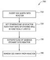
- FIG. 7 shows a method 700 for performing an epi-smoothing (i.e., etching) process upon the cleaved surface 152 of the SOI wafer 150 .
- the method 700 begins with the insertion of the SOI wafer 150 into a reactor.
- the SOI wafer 150 may be inserted into the reactor by any suitable device, such as a robotic manipulator.
- the reactor may be any suitable epitaxial deposition and/or smoothing reactor suitable for performing the epi-smoothing process upon SOI wafers.
- the reactor typically has one or more lamps or other mechanisms to heat the interior of the reactor.
- the temperature within the reactor is then set in block 720 such that the etching reaction will be kinetically limited, as opposed to being transport limited.
- the temperature is then set in block 720 such that the etching reaction will be kinetically limited, as opposed to being transport limited.
- by setting and controlling the temperature such that the epi-smoothing reaction will be kinetically limited results in a more uniform thickness over the cleaved surface 152 of the SOI wafer 150 .
- the rate of reaction is kinetically limited, the difference in the rate from the center of the SOI wafer 150 to the outer edge is reduced. Instead of increasing at the edges of the SOI wafer 150 , the rate of reaction is relatively uniform across the surface of the SOI wafer 150 .
- the temperature at which the etching reaction is kinetically limited is between 900° C. and 950° C.
- the reduced temperature corresponding to the kinetic limitation of the rate of deposition also permits colder offset temperatures to be used.
- the three offset zones are the front, side, and rear.
- the offset zone temperature set points are adjusted with respect to the center zone temperature set point. Accordingly, a lower set point for the center zone results in a lower set point used in the offset zones.
- the flow of gaseous etchant into the reactor is initiated.
- the flow of gaseous etchant is initiated immediately after the SOI wafer 150 is inserted in the reactor.
- the temperature of the reactor is already set at the proper temperature to ensure that the etching reaction will be kinetically limited.
- the gaseous etchant may be a mixture of HCl or chlorine and H 2 according to some embodiments.
- the flow of gaseous etchant into the reactor then continues for a period of time.
- the length of the period of time may be determined based on the amount of silicon that is to be removed from the cleaved surface 152 of the SOI wafer and the rate at which the silicon is being etched. For example, if the rate of etching is 3.0 Angstroms/sec and the amount of silicon to be removed is 900 Angstroms, then the SOI wafer will be removed from the reactor 300 seconds after the flow of gaseous etchant was initiated.
- the flow of gaseous etchant is then stopped after the desired amount of silicon has been removed by the flow of gaseous etchant.
- the SOI wafer 150 is then removed from the reactor.
- the SOI wafer 150 may be removed from the reactor by a robotic transport system.
- the SOI wafer 150 may remain in the reactor and be subjected to an epi-deposition process in the same reactor, as described below in relation to FIG. 8 .
- FIG. 8 shows a method 800 for performing an epi-deposition process upon the cleaved surface 152 of the SOI wafer 150 .
- the method 800 begins with the insertion of the SOI wafer 150 into a reactor.
- the SOI wafer 150 may be inserted into the reactor by any suitable device, such as by a robot.
- the reactor may be of the same type described above in regards to FIG. 7 .
- the wafer may already be disposed in the reactor.
- the temperature within the reactor is then set in block 820 such that the rate of deposition is kinetically limited, as opposed to being transport limited.
- setting and controlling the temperature such that the rate of deposition is kinetically limited results in a more uniform thickness gradient over the cleaved surface 152 of the SOI wafer 150 .
- the rate of deposition is kinetically limited the difference in the thickness of the deposited layer of silicon from the center of the SOI wafer 150 to the outer edge is reduced. Instead of increasing at edges of the SOI wafer 150 , the thickness of the deposited layer is relatively uniform across the surface of the wafer.
- the temperature at which the rate of deposition is kinetically limited is between about 950° C.
- the kinetically limited temperature range may be different.
- the kinetically limited growth temperature range is somewhat lower than that for trichlorosilane.
- the reduced temperature corresponding to the kinetic limitation of the rate of deposition also permits colder offset temperatures in the reactor to be used. The colder offset temperatures may be used to effectively control the thickness profile of the cleaved surface 152 near the terrace 160 .
- the deposition gas may be any of monosilane, dichlorosilane, trichlorosilane, tetrachlorosilane, or any other suitable gas.
- the deposition gas may include hydrogen.
- the flow of deposition gas is initiated immediately after the SOI wafer 150 is inserted in the reactor. In these embodiments, the temperature of the reactor is already set at the proper temperature to ensure that the rate of deposition (i.e., growth rate) will be kinetically limited.
- the decreased temperatures associated with kinetically limiting the rate of deposition also permit the usage of higher flow rates of deposition gases.
- the higher flow rate of deposition gases also result in reduced recirculation flows of the deposition gas due to the reduced Rayleigh number of the deposition gas. The reduced recirculation flow further reduces the amount of silicon deposited on the walls of the reactor by the deposition gas.
- the flow of deposition gas into the reactor then continues for a period of time.
- the length of the period of time may be determined based on the amount of silicon that is to be deposited onto the cleaved surface 152 of the SOI wafer and the rate at which the silicon is being deposited. For example, if the rate of deposition is 220 Angstroms/sec and the amount of silicon to be deposited is 13200 Angstroms (1.32 microns), then the SOI wafer will be removed from the reactor (or the flow of deposition gas ceased) 60 seconds after the flow of deposition gas was initiated.
- the flow of deposition gas is then stopped after the desired amount of silicon has been deposited on the cleaved surface 152 of the SOI wafer.
- the SOI wafer 150 is then removed from the reactor.
- the SOI wafer 150 may be removed from the reactor by a robotic transport system.
- the chart depicted in FIG. 9 shows the relationship between temperature and the rate of etching of the surface of an SOI wafer. As can be clearly seen in FIG. 9 , the rate of etching dramatically decreases as the temperatures decreases below 950° C. It is believed that at or about 950° C. the etching reaction ceases to be transport limited and instead becomes kinetically limited.
- FIGS. 10A-10C show the relationship between the rate of etching of the surface of an SOI wafer at varying distances from the center of wafer (in this case a 200 mm SOI wafer).
- FIG. 10A shows the relationship for an epi-smoothing process carried out at 1100° C.
- FIG. 10B shows the relationship when carried out at 950° C.
- FIG. 10C shows the relationship at 900° C.
- FIGS. 10A and 10B show the relationship in previously used temperatures.
- the rate of etching during an epi-smoothing process increases towards the edge of a wafer.
- This increase in the rate of etching results in a corresponding decrease in the thickness of the wafer at or near the edge of the wafer, thus creating a sharp thickness gradient at or near the edge of the wafer.
- FIG. 10C however shows the relationship between the etching rate and the distance from the center of the wafer according to the methods described above in FIG. 7 where the reaction is kinetically limited, and not transport limited. As can be seen in FIG.
- the non-uniformity in the rate of etching near the edges of the wafer is reduced approximately by a factor of four when compared to FIGS. 10A and 10B .
- the temperature where the reaction is kinetically limited, and not transport limited is between approximately 900° C. and 950° C.
- the chart depicted in FIG. 11 shows the relationship between temperature and the rate of deposition on the surface of an SOI wafer. As can be clearly seen in FIG. 11 , the rate of deposition dramatically decreases as the temperatures decreases below 950° C. It is believed that at or about 950° C. the deposition reaction ceases to be transport limited and instead becomes kinetically limited.
Abstract
Description
Claims (18)
Priority Applications (1)
| Application Number | Priority Date | Filing Date | Title |
|---|---|---|---|
| US12/971,788 US8080464B2 (en) | 2009-12-29 | 2010-12-17 | Methods for processing silicon on insulator wafers |
Applications Claiming Priority (2)
| Application Number | Priority Date | Filing Date | Title |
|---|---|---|---|
| US29078709P | 2009-12-29 | 2009-12-29 | |
| US12/971,788 US8080464B2 (en) | 2009-12-29 | 2010-12-17 | Methods for processing silicon on insulator wafers |
Publications (2)
| Publication Number | Publication Date |
|---|---|
| US20110159668A1 US20110159668A1 (en) | 2011-06-30 |
| US8080464B2 true US8080464B2 (en) | 2011-12-20 |
Family
ID=43589593
Family Applications (1)
| Application Number | Title | Priority Date | Filing Date |
|---|---|---|---|
| US12/971,788 Active US8080464B2 (en) | 2009-12-29 | 2010-12-17 | Methods for processing silicon on insulator wafers |
Country Status (8)
| Country | Link |
|---|---|
| US (1) | US8080464B2 (en) |
| EP (1) | EP2519962A1 (en) |
| JP (1) | JP5681209B2 (en) |
| KR (4) | KR20190129145A (en) |
| CN (1) | CN102687237A (en) |
| SG (1) | SG181556A1 (en) |
| TW (1) | TWI528443B (en) |
| WO (1) | WO2011082116A1 (en) |
Families Citing this family (4)
| Publication number | Priority date | Publication date | Assignee | Title |
|---|---|---|---|---|
| US9343379B2 (en) * | 2011-10-14 | 2016-05-17 | Sunedison Semiconductor Limited | Method to delineate crystal related defects |
| US9087687B2 (en) * | 2011-12-23 | 2015-07-21 | International Business Machines Corporation | Thin heterostructure channel device |
| US9202711B2 (en) * | 2013-03-14 | 2015-12-01 | Sunedison Semiconductor Limited (Uen201334164H) | Semiconductor-on-insulator wafer manufacturing method for reducing light point defects and surface roughness |
| US10332781B2 (en) * | 2014-12-19 | 2019-06-25 | Globalwafers Co., Ltd. | Systems and methods for performing epitaxial smoothing processes on semiconductor structures |
Citations (7)
| Publication number | Priority date | Publication date | Assignee | Title |
|---|---|---|---|---|
| WO2000063954A1 (en) | 1999-04-21 | 2000-10-26 | Silicon Genesis Corporation | Surface finishing of soi substrates using an epi process |
| US20020090818A1 (en) * | 1999-09-17 | 2002-07-11 | Anna Lena Thilderkvist | Apparatus and method for surface finishing a silicon film |
| US20040053515A1 (en) | 2002-09-12 | 2004-03-18 | Comita Paul B. | Apparatus and method for surface finishing a silicon film |
| US20070066036A1 (en) | 2005-09-22 | 2007-03-22 | Siltronic Ag | Epitaxially coated silicon wafer and method for producing epitaxially coated silicon wafers |
| US20070249139A1 (en) * | 2006-04-21 | 2007-10-25 | Kishor Purushottam Gadkaree | Semiconductor on glass insulator made using improved thinning process |
| EP1855309A1 (en) | 2005-02-28 | 2007-11-14 | Shin-Etsu Handotai Company Limited | Method for manufacturing bonded wafer and bonded wafer |
| US20090032873A1 (en) * | 2007-07-30 | 2009-02-05 | Jeffrey Scott Cites | Ultra thin single crystalline semiconductor TFT and process for making same |
Family Cites Families (7)
| Publication number | Priority date | Publication date | Assignee | Title |
|---|---|---|---|---|
| JPH01258416A (en) * | 1988-04-08 | 1989-10-16 | Nec Corp | Vapor growth method |
| JP3097107B2 (en) * | 1990-07-13 | 2000-10-10 | 日本電気株式会社 | Epitaxial growth method |
| JPH08162427A (en) * | 1994-12-01 | 1996-06-21 | Mitsubishi Electric Corp | Manufacture of semiconductor device |
| JP3358550B2 (en) * | 1998-07-07 | 2002-12-24 | 信越半導体株式会社 | Method for producing SOI wafer and SOI wafer produced by this method |
| JP2003249451A (en) * | 2002-02-22 | 2003-09-05 | Mitsubishi Electric Corp | Forming method for epitaxial thin film |
| US7294582B2 (en) * | 2002-07-19 | 2007-11-13 | Asm International, N.V. | Low temperature silicon compound deposition |
| US7976723B2 (en) * | 2007-05-17 | 2011-07-12 | International Business Machines Corporation | Method for kinetically controlled etching of copper |
-
2010
- 2010-12-17 US US12/971,788 patent/US8080464B2/en active Active
- 2010-12-23 CN CN2010800595318A patent/CN102687237A/en active Pending
- 2010-12-23 EP EP10801780A patent/EP2519962A1/en not_active Withdrawn
- 2010-12-23 JP JP2012547180A patent/JP5681209B2/en active Active
- 2010-12-23 KR KR1020197033430A patent/KR20190129145A/en not_active Application Discontinuation
- 2010-12-23 KR KR1020187036601A patent/KR20180137593A/en active Application Filing
- 2010-12-23 SG SG2012041851A patent/SG181556A1/en unknown
- 2010-12-23 KR KR1020127016847A patent/KR101787552B1/en active IP Right Grant
- 2010-12-23 KR KR1020177028852A patent/KR102155253B1/en active IP Right Grant
- 2010-12-23 WO PCT/US2010/062094 patent/WO2011082116A1/en active Application Filing
- 2010-12-29 TW TW099146707A patent/TWI528443B/en active
Patent Citations (10)
| Publication number | Priority date | Publication date | Assignee | Title |
|---|---|---|---|---|
| WO2000063954A1 (en) | 1999-04-21 | 2000-10-26 | Silicon Genesis Corporation | Surface finishing of soi substrates using an epi process |
| US6287941B1 (en) * | 1999-04-21 | 2001-09-11 | Silicon Genesis Corporation | Surface finishing of SOI substrates using an EPI process |
| US20070259526A1 (en) * | 1999-04-21 | 2007-11-08 | Silicon Genesis Corporation | Surface finishing of SOI substrates using an EPI process |
| US20020090818A1 (en) * | 1999-09-17 | 2002-07-11 | Anna Lena Thilderkvist | Apparatus and method for surface finishing a silicon film |
| US6562720B2 (en) | 1999-09-17 | 2003-05-13 | Applied Materials, Inc. | Apparatus and method for surface finishing a silicon film |
| US20040053515A1 (en) | 2002-09-12 | 2004-03-18 | Comita Paul B. | Apparatus and method for surface finishing a silicon film |
| EP1855309A1 (en) | 2005-02-28 | 2007-11-14 | Shin-Etsu Handotai Company Limited | Method for manufacturing bonded wafer and bonded wafer |
| US20070066036A1 (en) | 2005-09-22 | 2007-03-22 | Siltronic Ag | Epitaxially coated silicon wafer and method for producing epitaxially coated silicon wafers |
| US20070249139A1 (en) * | 2006-04-21 | 2007-10-25 | Kishor Purushottam Gadkaree | Semiconductor on glass insulator made using improved thinning process |
| US20090032873A1 (en) * | 2007-07-30 | 2009-02-05 | Jeffrey Scott Cites | Ultra thin single crystalline semiconductor TFT and process for making same |
Non-Patent Citations (4)
| Title |
|---|
| Habuka, Hitoshi et al., Change in Microroughness of a Silicon Surface during In Situ Cleaning Using HF and HCl Gases, Journal of the Electrochemical Society, Dec. 1, 1998, vol. 145, No. 12, pp. 4264-4271, Electrochemical Society, Manchester, NH. |
| Habuka, Hitoshi et al., Dominant rate process of silicon surface etching by hydrogen chloride gas, Science Direct, Oct. 1, 2005, pp. 104-110, Elsevier. |
| Habuka, Hitoshi et al., Nonlinear increase in silicon epitaxial growth rate in a SiHCl3-H2 system under atmospheric pressure, Journal of Crystal Growth, Dec. 1, 1997, pp. 359-362, vol. 182, No. 3-4, Elsevier, Amsterdam, NL. |
| PCT International Search Report and Written Opinion of the International Searching Authority mailed on Mar. 9, 2011 regarding PCT/US2010/062094 filed on Dec. 23, 2010. |
Also Published As
| Publication number | Publication date |
|---|---|
| SG181556A1 (en) | 2012-07-30 |
| JP5681209B2 (en) | 2015-03-04 |
| KR20120094076A (en) | 2012-08-23 |
| KR20170117612A (en) | 2017-10-23 |
| KR102155253B1 (en) | 2020-09-11 |
| EP2519962A1 (en) | 2012-11-07 |
| US20110159668A1 (en) | 2011-06-30 |
| KR20180137593A (en) | 2018-12-27 |
| CN102687237A (en) | 2012-09-19 |
| JP2013516085A (en) | 2013-05-09 |
| KR20190129145A (en) | 2019-11-19 |
| WO2011082116A1 (en) | 2011-07-07 |
| TW201140679A (en) | 2011-11-16 |
| TWI528443B (en) | 2016-04-01 |
| KR101787552B1 (en) | 2017-10-19 |
Similar Documents
| Publication | Publication Date | Title |
|---|---|---|
| US6291313B1 (en) | Method and device for controlled cleaving process | |
| US8859393B2 (en) | Methods for in-situ passivation of silicon-on-insulator wafers | |
| US7378330B2 (en) | Cleaving process to fabricate multilayered substrates using low implantation doses | |
| US7348258B2 (en) | Method and device for controlled cleaving process | |
| US6500732B1 (en) | Cleaving process to fabricate multilayered substrates using low implantation doses | |
| EP1194949B1 (en) | Surface finishing of soi substrates using an epi process | |
| CN105431936A (en) | Semiconductor-on-insulator wafer manufacturing method for reducing light point defects and surface roughness | |
| KR20080036209A (en) | Method for the manufacture of a strained silicon-on-insulator structure | |
| US7470600B2 (en) | Method and device for controlled cleaving process | |
| US8080464B2 (en) | Methods for processing silicon on insulator wafers | |
| US20100130021A1 (en) | Method for processing a silicon-on-insulator structure | |
| JP2013516085A5 (en) | ||
| EP3370249B1 (en) | Bonded soi wafer manufacturing method |
Legal Events
| Date | Code | Title | Description |
|---|---|---|---|
| AS | Assignment |
Owner name: MEMC ELECTRONIC MATERIALS, INC., MISSOURI Free format text: ASSIGNMENT OF ASSIGNORS INTEREST;ASSIGNORS:DHUMAL, SWAPNIL Y.;FLANNERY, LAWRENCE P.;TORACK, THOMAS A.;AND OTHERS;SIGNING DATES FROM 20110110 TO 20110127;REEL/FRAME:025897/0977 |
|
| STCF | Information on status: patent grant |
Free format text: PATENTED CASE |
|
| AS | Assignment |
Owner name: GOLDMAN SACHS BANK USA, NEW JERSEY Free format text: SECURITY AGREEMENT;ASSIGNORS:NVT, LLC;SUN EDISON LLC;SOLAICX, INC.;AND OTHERS;REEL/FRAME:029057/0810 Effective date: 20120928 |
|
| AS | Assignment |
Owner name: SOLAICX, OREGON Free format text: RELEASE BY SECURED PARTY;ASSIGNOR:GOLDMAN SACHS BANK USA;REEL/FRAME:031870/0092 Effective date: 20131220 Owner name: NVT, LLC, CALIFORNIA Free format text: RELEASE BY SECURED PARTY;ASSIGNOR:GOLDMAN SACHS BANK USA;REEL/FRAME:031870/0092 Effective date: 20131220 Owner name: SUN EDISON LLC, CALIFORNIA Free format text: RELEASE BY SECURED PARTY;ASSIGNOR:GOLDMAN SACHS BANK USA;REEL/FRAME:031870/0092 Effective date: 20131220 Owner name: SUNEDISON, INC. (F/K/A MEMC ELECTRONIC MATERIALS, Free format text: RELEASE BY SECURED PARTY;ASSIGNOR:GOLDMAN SACHS BANK USA;REEL/FRAME:031870/0092 Effective date: 20131220 |
|
| AS | Assignment |
Owner name: DEUTSCHE BANK AG NEW YORK BRANCH, NEW JERSEY Free format text: SECURITY AGREEMENT;ASSIGNORS:SUNEDISON, INC.;SOLAICX;SUN EDISON, LLC;AND OTHERS;REEL/FRAME:032177/0359 Effective date: 20140115 |
|
| AS | Assignment |
Owner name: SUN EDISON LLC, CALIFORNIA Free format text: RELEASE BY SECURED PARTY;ASSIGNOR:DEUTSCHE BANK AG NEW YORK BRANCH;REEL/FRAME:032382/0724 Effective date: 20140228 Owner name: SUNEDISON, INC., MISSOURI Free format text: RELEASE BY SECURED PARTY;ASSIGNOR:DEUTSCHE BANK AG NEW YORK BRANCH;REEL/FRAME:032382/0724 Effective date: 20140228 Owner name: NVT, LLC, MARYLAND Free format text: RELEASE BY SECURED PARTY;ASSIGNOR:DEUTSCHE BANK AG NEW YORK BRANCH;REEL/FRAME:032382/0724 Effective date: 20140228 Owner name: SOLAICX, OREGON Free format text: RELEASE BY SECURED PARTY;ASSIGNOR:DEUTSCHE BANK AG NEW YORK BRANCH;REEL/FRAME:032382/0724 Effective date: 20140228 |
|
| AS | Assignment |
Owner name: SUNEDISON SEMICONDUCTOR LIMITED (UEN201334164H), S Free format text: ASSIGNMENT OF ASSIGNORS INTEREST;ASSIGNOR:MEMC ELECTRONIC MATERIALS, INC.;REEL/FRAME:033023/0430 Effective date: 20140523 |
|
| AS | Assignment |
Owner name: SUNEDISON SEMICONDUCTOR TECHNOLOGY PTE. LTD., MISS Free format text: NOTICE OF LICENSE AGREEMENT;ASSIGNOR:SUNEDISON SEMICONDUCTOR LIMITED;REEL/FRAME:033099/0001 Effective date: 20140527 |
|
| FPAY | Fee payment |
Year of fee payment: 4 |
|
| AS | Assignment |
Owner name: GLOBALWAFERS CO., LTD., TAIWAN Free format text: ASSIGNMENT OF ASSIGNORS INTEREST;ASSIGNORS:SUNEDISON SEMICONDUCTOR LIMITED;MEMC JAPAN LIMITED;MEMC ELECTRONIC MATERIALS S.P.A.;REEL/FRAME:046327/0001 Effective date: 20180606 |
|
| MAFP | Maintenance fee payment |
Free format text: PAYMENT OF MAINTENANCE FEE, 8TH YEAR, LARGE ENTITY (ORIGINAL EVENT CODE: M1552); ENTITY STATUS OF PATENT OWNER: LARGE ENTITY Year of fee payment: 8 |
|
| MAFP | Maintenance fee payment |
Free format text: PAYMENT OF MAINTENANCE FEE, 12TH YEAR, LARGE ENTITY (ORIGINAL EVENT CODE: M1553); ENTITY STATUS OF PATENT OWNER: LARGE ENTITY Year of fee payment: 12 |