US8098353B2 - Liquid crystal display with improved response speed and aperture ratio - Google Patents
Liquid crystal display with improved response speed and aperture ratio Download PDFInfo
- Publication number
- US8098353B2 US8098353B2 US12/187,683 US18768308A US8098353B2 US 8098353 B2 US8098353 B2 US 8098353B2 US 18768308 A US18768308 A US 18768308A US 8098353 B2 US8098353 B2 US 8098353B2
- Authority
- US
- United States
- Prior art keywords
- inclination direction
- liquid crystal
- pixel electrode
- crystal display
- direction determining
- Prior art date
- Legal status (The legal status is an assumption and is not a legal conclusion. Google has not performed a legal analysis and makes no representation as to the accuracy of the status listed.)
- Active, expires
Links
Images


Classifications
-
- G—PHYSICS
- G02—OPTICS
- G02F—OPTICAL DEVICES OR ARRANGEMENTS FOR THE CONTROL OF LIGHT BY MODIFICATION OF THE OPTICAL PROPERTIES OF THE MEDIA OF THE ELEMENTS INVOLVED THEREIN; NON-LINEAR OPTICS; FREQUENCY-CHANGING OF LIGHT; OPTICAL LOGIC ELEMENTS; OPTICAL ANALOGUE/DIGITAL CONVERTERS
- G02F1/00—Devices or arrangements for the control of the intensity, colour, phase, polarisation or direction of light arriving from an independent light source, e.g. switching, gating or modulating; Non-linear optics
- G02F1/01—Devices or arrangements for the control of the intensity, colour, phase, polarisation or direction of light arriving from an independent light source, e.g. switching, gating or modulating; Non-linear optics for the control of the intensity, phase, polarisation or colour
- G02F1/13—Devices or arrangements for the control of the intensity, colour, phase, polarisation or direction of light arriving from an independent light source, e.g. switching, gating or modulating; Non-linear optics for the control of the intensity, phase, polarisation or colour based on liquid crystals, e.g. single liquid crystal display cells
- G02F1/133—Constructional arrangements; Operation of liquid crystal cells; Circuit arrangements
- G02F1/1333—Constructional arrangements; Manufacturing methods
- G02F1/1337—Surface-induced orientation of the liquid crystal molecules, e.g. by alignment layers
- G02F1/133707—Structures for producing distorted electric fields, e.g. bumps, protrusions, recesses, slits in pixel electrodes
-
- G—PHYSICS
- G02—OPTICS
- G02F—OPTICAL DEVICES OR ARRANGEMENTS FOR THE CONTROL OF LIGHT BY MODIFICATION OF THE OPTICAL PROPERTIES OF THE MEDIA OF THE ELEMENTS INVOLVED THEREIN; NON-LINEAR OPTICS; FREQUENCY-CHANGING OF LIGHT; OPTICAL LOGIC ELEMENTS; OPTICAL ANALOGUE/DIGITAL CONVERTERS
- G02F1/00—Devices or arrangements for the control of the intensity, colour, phase, polarisation or direction of light arriving from an independent light source, e.g. switching, gating or modulating; Non-linear optics
- G02F1/01—Devices or arrangements for the control of the intensity, colour, phase, polarisation or direction of light arriving from an independent light source, e.g. switching, gating or modulating; Non-linear optics for the control of the intensity, phase, polarisation or colour
- G02F1/13—Devices or arrangements for the control of the intensity, colour, phase, polarisation or direction of light arriving from an independent light source, e.g. switching, gating or modulating; Non-linear optics for the control of the intensity, phase, polarisation or colour based on liquid crystals, e.g. single liquid crystal display cells
- G02F1/133—Constructional arrangements; Operation of liquid crystal cells; Circuit arrangements
- G02F1/1333—Constructional arrangements; Manufacturing methods
- G02F1/1343—Electrodes
-
- G—PHYSICS
- G02—OPTICS
- G02F—OPTICAL DEVICES OR ARRANGEMENTS FOR THE CONTROL OF LIGHT BY MODIFICATION OF THE OPTICAL PROPERTIES OF THE MEDIA OF THE ELEMENTS INVOLVED THEREIN; NON-LINEAR OPTICS; FREQUENCY-CHANGING OF LIGHT; OPTICAL LOGIC ELEMENTS; OPTICAL ANALOGUE/DIGITAL CONVERTERS
- G02F1/00—Devices or arrangements for the control of the intensity, colour, phase, polarisation or direction of light arriving from an independent light source, e.g. switching, gating or modulating; Non-linear optics
- G02F1/01—Devices or arrangements for the control of the intensity, colour, phase, polarisation or direction of light arriving from an independent light source, e.g. switching, gating or modulating; Non-linear optics for the control of the intensity, phase, polarisation or colour
- G02F1/13—Devices or arrangements for the control of the intensity, colour, phase, polarisation or direction of light arriving from an independent light source, e.g. switching, gating or modulating; Non-linear optics for the control of the intensity, phase, polarisation or colour based on liquid crystals, e.g. single liquid crystal display cells
- G02F1/133—Constructional arrangements; Operation of liquid crystal cells; Circuit arrangements
- G02F1/1333—Constructional arrangements; Manufacturing methods
- G02F1/1337—Surface-induced orientation of the liquid crystal molecules, e.g. by alignment layers
- G02F1/133742—Surface-induced orientation of the liquid crystal molecules, e.g. by alignment layers for homeotropic alignment
-
- G—PHYSICS
- G02—OPTICS
- G02F—OPTICAL DEVICES OR ARRANGEMENTS FOR THE CONTROL OF LIGHT BY MODIFICATION OF THE OPTICAL PROPERTIES OF THE MEDIA OF THE ELEMENTS INVOLVED THEREIN; NON-LINEAR OPTICS; FREQUENCY-CHANGING OF LIGHT; OPTICAL LOGIC ELEMENTS; OPTICAL ANALOGUE/DIGITAL CONVERTERS
- G02F2201/00—Constructional arrangements not provided for in groups G02F1/00 - G02F7/00
- G02F2201/40—Arrangements for improving the aperture ratio
Definitions
- the present invention relates to a liquid crystal display and more particularly, to a liquid crystal display having an improved response speed and aperture ratio.
- LCDs are one of the most widely used flat panel displays, and an LCD includes a pair of panels provided with field-generating electrodes, such as pixel electrodes and a common electrode, and a liquid crystal (“LC”) layer interposed between the two panels.
- the LCD displays images by applying voltages to the field-generating electrodes to generate an electric field in the LC layer that determines the orientations of LC molecules therein to adjust polarization of incident light.
- An LCD also includes switching elements connected to the respective pixel electrodes and a plurality of signal lines such as gate lines and data lines for controlling the switching elements and thereby applying voltages to the pixel electrodes.
- the degree of orientation of LC molecules in the LC layer may be varied by applying voltages of various magnitudes to the pixel electrodes.
- a typical LCD has a plurality of discreet gray levels corresponding to orientations of the LC molecules between the black and white displays.
- a vertical alignment (“VA”) mode LCD which aligns LC molecules such that the long axes of the LC molecules are perpendicular to the panels in the absence of an electric field, has become increasingly popular because of its high contrast ratio and wide reference viewing angle.
- a wide reference viewing angle is defined as a viewing angle that makes the contrast ratio equal to about 1:10 or as a limit angle for inversion in luminance between the gray levels.
- the wide viewing angle of the VA mode LCD can be realized by cutouts in the field-generating electrodes and protrusions on the field-generating electrodes. Since the cutouts and protrusions can determine tilt directions of the LC molecules, the tilt directions can be distributed in several directions by using the cutouts and protrusions such that a reference viewing angle is widened.
- the present invention provides a liquid crystal display (“LCD”) with an improved response speed and aperture ratio.
- LCD liquid crystal display
- An exemplary embodiment of a liquid crystal display (“LCD”) includes; a gate line, a data line disposed substantially perpendicular to the gate line, a switching element connected to the gate line and the data line, a pixel electrode connected to the switching element, and having a first inclination direction determining member including at least one first oblique portion forming an oblique angle with the gate line and the data line, and an inclination direction assistance member disposed adjacent to the first inclination direction determining member, and substantially parallel to the first oblique portion.
- the inclination direction assistance member may include a step portion formed in the pixel electrode.
- an insulating layer may be disposed between the data line and the pixel electrode, and the inclination direction assistance member may include a recess portion formed in the insulating layer and corresponding to the step portion of the pixel electrode.
- the width of the recess portion is about 4 ⁇ m to about 8 ⁇ m.
- the depth of the recess portion may be about 500 ⁇ to about 2500 ⁇ .
- a common electrode disposed substantially opposite to the pixel electrode may be further included, and the common electrode may include a second inclination direction determining member having at least one second oblique portion substantially parallel to the first oblique portion and disposed substantially opposite to the first inclination direction determining member with respect to the inclination direction assistance member.
- the horizontal distance between the first inclination direction determining member and the second inclination direction determining member may be substantially equal to or greater than about 40 ⁇ m.
- the ratio of the distance between the second inclination direction determining member and the inclination direction assistance member to the distance between the first inclination direction determining member and the inclination direction assistance member may be from about 1:3 to about 1:1.
- the horizontal distance between the inclination direction assistance member and the first inclination direction determining member may be smaller than the horizontal distance between the inclination direction assistance member and the second inclination direction determining member.
- the ratio of the horizontal distance between the second inclination direction determining member and the inclination direction assistance member to the horizontal distance between the first inclination direction determining member and the inclination direction assistance member ranges from about 1:1 to about 3:1.
- a method of increasing an aperture ratio and response speed of a liquid crystal display includes; disposing a gate line on a substrate, disposing a data line substantially perpendicular to the gate line, disposing a switching element in connection with the gate line and the data line, disposing a pixel electrode in connection with the switching element, and having a first inclination direction determining member comprising at least one first oblique portion forming an oblique angle with the gate line and the data line, and forming an inclination direction assistance member adjacent to the first inclination direction determining member, and substantially parallel to the first oblique portion.
- FIG. 1 is a layout view of an exemplary embodiment of a lower panel for an exemplary embodiment of a liquid crystal display (“LCD”) according to the present invention
- FIG. 2 is a layout view of an exemplary embodiment of an upper panel for an exemplary embodiment of an LCD according to the present invention
- FIG. 3 is a layout view of an exemplary embodiment of an LCD including the exemplary embodiments of a lower panel shown in FIG. 1 and the exemplary embodiment of an upper panel shown in FIG. 2 ;
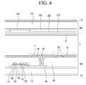
- FIG. 4 and FIG. 5 are cross-sectional views of the exemplary embodiment of an LCD shown in FIG. 3 taken along lines IV-IV and V-V, respectively;
- FIG. 6 is an enlarged view of a portion of the exemplary embodiment of an LCD shown in FIG. 3 ;
- FIG. 7 is a cross-sectional view of FIG. 6 taken alone line VII-VII;
- FIG. 8A is a photograph showing a response speed of an LCD according to the prior art
- FIG. 8B is a photograph showing a response speed of an exemplary embodiment of an LCD according to the present invention.
- first,” “second,” “third” etc. may be used herein to describe various elements, components, regions, layers and/or sections, these elements, components, regions, layers and/or sections should not be limited by these terms. These terms are only used to distinguish one element, component, region, layer or section from another element, component, region, layer or section. Thus, a first element, component, region, layer or section discussed below could be termed a second element, component, region, layer or section without departing from the teachings of the present invention.
- relative terms such as “lower” or “bottom” and “upper” or “top” may be used herein to describe one element's relationship to other elements as illustrated in the Figures. It will be understood that relative terms are intended to encompass different orientations of the device in addition to the orientation depicted in the Figures. For example, if the device in one of the figures is turned over, elements described as being on the “lower” side of other elements would then be oriented on the “upper” side of the other elements. The exemplary term “lower” can, therefore, encompass both an orientation of “lower” and “upper,” depending upon the particular orientation of the figure.
- Exemplary embodiments of the present invention are described herein with reference to cross section illustrations which are schematic illustrations of idealized embodiments of the present invention. As such, variations from the shapes of the illustrations as a result, for example, of manufacturing techniques and/or tolerances, are to be expected. Thus, embodiments of the present invention should not be construed as limited to the particular shapes of regions illustrated herein but are to include deviations in shapes which result, for example, from manufacturing. For example, a region illustrated or described as flat may, typically, have rough and/or nonlinear features. Moreover, sharp angles which are illustrated may be rounded. Thus, the regions illustrated in the figures are schematic in nature and their shapes are not intended to illustrate the precise shape of a region and are not intended to limit the scope of the present invention.
- FIG. 1 is a layout view of an exemplary embodiment of a lower panel for an exemplary embodiment of a liquid crystal display (“LCD”) according to the present invention
- FIG. 2 is a layout view of an exemplary embodiment of an upper panel for an exemplary embodiment of an LCD according to the present invention
- FIG. 3 is a layout view of an exemplary embodiment of an LCD including the exemplary embodiment of a lower panel shown in FIG. 1 and the exemplary embodiment of an upper panel shown in FIG. 2
- FIG. 4 and FIG. 5 are cross-sectional views of the exemplary embodiment of an LCD shown in FIG. 3 taken along lines IV-IV and V-V, respectively.
- an exemplary embodiment of an LCD according to the present invention includes a lower panel 100 and an upper panel 200 opposing the lower panel 100 , and a liquid crystal layer 3 interposed between the two panels 100 and 200 .
- the lower panel 100 will be described in detail with reference to FIG. 1 , FIG. 3 , FIG. 4 and FIG. 5 .
- a plurality of gate lines 121 and a plurality of storage electrode lines 131 are formed on an insulating substrate 110 , one exemplary embodiment of which is made of transparent glass or plastic.
- the gate lines 121 which are separated from each other, extend substantially in a transverse direction and transmit gate signals.
- Each gate line 121 includes a plurality of gate electrodes 124 protruding from the gate line 121 , and an end portion 129 having a large area for connection with another layer or an external driving circuit (not shown).
- a gate driving circuit (not shown) for generating the gate signals may be mounted on a flexible printed circuit (“FPC”) film (not shown), which may be attached to the substrate 110 , directly mounted on the substrate 110 , or integrated with the substrate 110 .
- Alternative exemplary embodiments include configurations wherein the gate lines 121 may extend to be connected to a driving circuit that may be integrated with the substrate 110 and the end portion 129 may be omitted.
- the storage electrode lines 131 extend substantially in a transverse direction and are substantially parallel to the gate lines 121 , and are supplied with a predetermined voltage.
- Each storage electrode line 131 includes a stem line and a plurality of first and second storage electrodes 137 a and 137 b branched from the stem line.
- Each storage electrode line 131 is disposed between two neighboring gate lines 121 .
- the first and second storage electrodes 137 a and 137 b are extended in a substantially vertical direction and substantially opposite to each other.
- alternative exemplary embodiments include the shapes of the storage electrode lines 131 may be variously changed.
- a gate insulating layer 140 is formed on the gate lines 121 and the storage electrode lines 131 .
- a plurality of semiconductor islands 154 is formed on the gate insulating layer 140 .
- the semiconductor islands 154 are disposed on the gate electrodes 124 .
- a pair of ohmic contact islands 163 and 165 is formed on the semiconductor islands 154 .
- Exemplary embodiments of the ohmic contacts 163 and 165 can be made of a material such as n+ hydrogenated amorphous silicon with an n-type impurity, such as phosphor doped at high concentration and silicide.
- a plurality of data conductors including a plurality of data lines 171 and a plurality of drain electrodes 175 are formed on the ohmic contacts 163 and 165 , and the gate insulation layer 140 .
- the data lines 171 transfer a data signal and extend in a substantially vertical direction, thereby crossing the gate lines 121 and the storage electrode lines 131 .
- Each data line 171 includes a plurality of source electrodes 173 extending toward the gate electrodes 124 with a ‘U’ shape, and, in one exemplary embodiment, a wide end 179 for connected to another layer or an external driving circuit.
- the data line 171 may extend to thereby directly connect thereto.
- each drain electrode 175 is separated from the data lines 171 and face the source electrodes 173 with respect to the gate electrodes 124 .
- each drain electrode 175 includes one end portion having a large area for contacting with another layer and another end portion disposed on a gate electrode 124 and partly enclosed by a source electrode 173 .
- the ohmic contacts 163 and 165 are interposed only between the underlying semiconductors 154 and the overlying data lines 171 and drain electrodes 175 thereon, and reduce the contact resistance therebetween.
- the semiconductors 154 include a plurality of exposed portions that are not covered with the data lines 171 and the drain electrodes 175 , such as portions located between the source electrodes 173 and the drain electrodes 175 .
- the gate electrodes 124 , source electrodes 173 , drain electrodes 175 and semiconductors 154 form a plurality of thin film transistors (TFTs) on the insulating substrate 110 .
- TFTs thin film transistors
- a passivation layer 180 is formed on the data conductors 171 and 175 and the exposed semiconductors 154 .
- the passivation layer 180 is made of an inorganic insulator, an organic insulator, or a double-layered structure including an inorganic insulator and an organic insulator.
- the passivation layer 180 may be flattened.
- the passivation layer 180 includes a plurality of recess portions 60 .
- the recess portion 60 includes first lower and upper recess portions 61 a and 61 b , second lower and upper recess portions 62 a and 62 b , third lower and upper recess portions 63 a and 63 b , and fourth lower and upper recess portions 64 a and 64 b.
- the passivation layer 180 has a plurality of contact holes 182 and 185 exposing the end portions 179 of the data lines 171 , and the end portions of the drain electrodes 175 , respectively, and the passivation layer 180 and the gate insulating layer 140 have a plurality of contact holes 181 exposing the end portions 129 of the gate lines 121 .
- a plurality of pixel electrodes 191 , and a plurality of contact assistants 81 and 82 are formed on the passivation layer 180 .
- a transparent conductor such as ITO or IZO
- a reflective conductor such as Al, Cr, or alloys thereof
- the pixel electrodes 191 are physically and electrically connected to the drain electrodes 175 through the contact holes 185 such that the pixel electrodes 191 receive the data voltages from the drain electrodes 175 .
- the pixel electrodes 191 supplied with the data voltages generate electric fields in cooperation with a common electrode 270 supplied with a common voltage and provided in the common electrode panel 200 , which determine the orientations of liquid crystal molecules in a liquid crystal layer 3 .
- the polarization of light passing through the liquid crystal layer 3 varies according to the direction of the liquid crystal molecules.
- the pixel electrode 191 and the common electrode 270 form a liquid crystal capacitor, which stores applied voltages after turn-off of the TFT.
- the storage capacitors are implemented by overlapping the pixel electrodes 191 with the storage electrode lines 131 as well as the storage electrodes 137 a and 137 b.
- Each pixel electrode 191 has a substantially rectangular shape having four main edges substantially parallel to the gate lines 121 and the data lines 171 , and chamfered left corners.
- the chamfered oblique sides 90 a and 90 b of the pixel electrodes 191 are inclined with respect to the gate lines 121 by an angle of about 45°; in other words, the chamfered oblique sides 90 a and 90 b of the pixel electrode 191 are disposed to form an angle of about 45° with the gate lines 121 as seen from a top plan view.
- Each pixel electrode 191 includes first and second central cutouts 91 and 92 and is divided into a plurality of partitions by these cutouts 91 and 92 .
- the cutout portions 91 and 92 are each substantially symmetric with respect to a virtual horizontal central line which bisects the pixel electrode 191 .
- the first central cutout 91 includes a substantially vertical portion and a pair of oblique portions connected to the substantially vertical portion.
- the substantially vertical portion is disposed substantially perpendicular to the horizontal central line of the pixel electrode 191 , and the pair of oblique portions are respectively extended toward the right edge of the pixel electrode 191 from the substantially vertical portion, wherein the oblique portions extend at an angle of about 45° from the substantially vertical portion and at an angle of about 45° with respect to the gate lines 121 .
- the oblique portions are substantially perpendicular to each other.
- the second central cutout 92 extends along the horizontal central line of the pixel electrode 191 and has an inlet from the right edge of the pixel electrode 191 , which has a pair of inclined edges disposed substantially parallel to the oblique portions of the first central cutout 91 .
- the lower half of the pixel electrode 191 is substantially partitioned into two lower partitions by the oblique portion of the first central cutout 91 .
- the upper half of the pixel electrode 191 is partitioned into two upper partitions by the oblique portion of the first central cutout 91 .
- the number of partitions and the number of cutouts can be varied depending on design factors such as the size of pixels, the ratio of the transverse edges and the longitudinal edges of the pixel electrodes, the type and characteristics of the liquid crystal layer 3 , and so on.
- the contact assistants 81 and 82 are connected to the end portions 129 of the gate lines 121 and the end portions 179 of the data lines 171 through the contact holes 181 and 182 , respectively.
- the contact assistants 81 and 82 protect the end portions 129 and 179 and complement the adhesion of the end portions 129 and 179 with external devices.
- a light blocking member 220 also called a black matrix, for preventing light leakage is formed on an insulating substrate 210 .
- the insulating substrate 210 include transparent glass or other similar materials.
- the light blocking member 220 includes linear portions corresponding to the data lines 171 and other portions corresponding to the TFTs, prevents light leakage between the pixel electrodes 191 , and defines a plurality of openings which face the pixel electrodes 191 .
- the light blocking member 220 may include a plurality of openings which face, and have substantially the same planar shape as, the pixel electrodes 191 .
- a plurality of color filters 230 are formed on the substrate 210 .
- the color filters 230 are disposed substantially in the areas enclosed by the light blocking member 220 , and may extend substantially along the longitudinal direction along the pixel electrodes 191 .
- the color filters 230 may represent one of the primary colors, such as red, green, and blue colors.
- An overcoat 250 for preventing the color filters 230 from being exposed and for providing a flat surface is formed on the color filters 230 and the light blocking member 220 .
- the overcoat 250 may be omitted.
- a common electrode 270 is formed on the overcoat 250 .
- the common electrode 270 is made of a transparent conductive material, exemplary embodiments of which include ITO and IZO, and has a plurality of sets of cutouts 70 .
- a set of cutouts 70 faces the pixel electrode 191 .
- the cutouts 70 include a lower cutout 72 a , a center cutout 71 , and an upper cutout 72 b .
- Each of the cutouts 71 - 72 b is disposed between adjacent cutouts 91 - 92 of the pixel electrode 191 or between the cutout 92 and the chamfered edges 90 a and 90 b of the pixel electrodes 191 .
- each of the cutouts 70 has at least one oblique portion extending substantially parallel to the oblique portion of the first central cutout 91 of the pixel electrode 191 .
- Each cutout 70 is substantially symmetric with respect to the above-described transverse line bisecting the pixel electrode 191 .
- Each of the lower and upper cutouts 72 a and 72 b includes an oblique portion extending approximately from a left edge of the pixel electrode 191 to approximately a lower or upper edge, respectively, of the pixel electrode 191 .
- Each of the lower and upper cutouts 72 a and 72 b also include transverse and longitudinal portions extending from respective ends of the oblique portion along edges of the pixel electrode 191 , overlapping the edges of the pixel electrode 191 , and making obtuse angles with the oblique portion.
- the center cutout 71 includes a central transverse portion extending approximately from the left edge of the pixel electrode 191 along the transverse central line of the pixel electrode 191 , a pair of oblique portions extending from an end of the central transverse portion approximately to a right edge of the pixel electrode 191 and making obtuse angles with the central transverse portion, and a pair of terminal longitudinal portions extending from the ends of the respective oblique portions along the right edge of the pixel electrode 191 , overlapping the right edge of the pixel electrode 191 , and making obtuse angles with the respective oblique portions.
- the number of cutouts 70 may be varied depending on design factors, and the light blocking member 220 may also overlap the cutouts 70 to block light leakage through the cutouts 70 .
- the cutouts 70 and 90 may be substituted with protrusions (not shown) or depressions (not shown).
- the protrusions may be made of an organic or inorganic material and disposed on or under the field-generating electrodes 191 or 270 .
- the cutouts 70 and 90 , or the protrusions (not shown) or depressions (not shown) form inclination direction determining members which determine an inclination direction of the liquid crystal molecules in the LCD.
- the recess portion 60 of the passivation layer 180 is disposed between the cutout 90 of the pixel electrode 191 or the chamfered edges 90 a and 90 b and the cutout 70 of the common electrode 270 . That is, the first lower and upper recess portions 61 a and 61 b are disposed between the central cutout 71 of the common electrode 270 and the first central cutout 91 of the pixel electrode 191 , the second lower recess portion 62 a is disposed between the first central cutout 91 of the pixel electrode 191 and the lower cutout 72 a of the common electrode 270 , the second upper recess portion 62 b is disposed between the first central cutout 91 of the pixel electrode 191 and the upper cutout 72 b of the common electrode 270 , the third lower recess portion 63 a is disposed between the lower cutout 72 a of the common electrode 270 and the chamfered edge 90 a of the pixel electrode 191 , the third upper recess portion
- FIG. 6 is an enlarged view of the dotted circle portion of the exemplary embodiment of an LCD shown in FIG. 3
- FIG. 7 is a cross-sectional view of FIG. 6 taken alone line VII-VII.
- the recess 60 portion of the passivation layer 180 is disposed between the cutout 90 of the pixel electrode 191 and the cutout 70 of the common electrode 270 .
- a step portion 191 a is formed in the pixel electrode 191 , wherein the step portion 191 a is aligned with the recess portion 60 of the passivation layer 180 .
- the step portion 191 a forms an inclination direction assistance member which assists in inclining liquid crystal molecules in an LCD as described in more detail below.
- a distance A between the cutout 90 of the pixel electrode 191 and the cutout 70 of the common electrode 270 is more than or equal to about 40 ⁇ m in width in order to increase an aperture ratio of the LCD.
- a distance C between the cutout 70 of the common electrode 270 and the recess portion 60 may be compared with a distance B between the cutout 90 of the pixel electrode 191 and the recess portion 60 to generate a C:B ratio.
- the C:B ratio may be in a range of from about 1:1 to about 1:3. In another exemplary embodiment, the C:B ratio may be in a range from about 1:1 to about 3:1.
- the width D of the recess portion 60 is in a range of from about 4 ⁇ m to about 8 ⁇ m, and a depth E of the recess portion 60 is in a range from about 500 ⁇ to about 2500 ⁇ to sufficiently form the step portion 191 a of the pixel electrode 191 .
- the cutouts 71 to 72 b and 91 to 92 of the field generating electrodes 191 and 270 and the sides of the pixel electrodes 191 generate a horizontal component to the generated electric field.
- the horizontal component of the electric field determines the oblique direction of the liquid crystal molecules by transforming the main electric field.
- the horizontal component of the electric field is substantially perpendicular to the sides of the cutouts 70 and 90 and the sides of the pixel electrodes 191 .
- these sub-areas may also be called “domains”, are formed to be substantially perpendicular to the primary edges of the pixel electrode 191 .
- Each sub-area is differently affected by the horizontal components of the electric field resulting from the individual configuration of the cutouts 70 and 90 in that particular sub-area.
- the aperture ratio of the liquid crystal display is also correspondingly increased.
- the portions disposed away from the cutouts 70 and 90 between the respective cutouts 70 and 90 receive very little influence from the horizontal component of the main electric field that is transformed by the cutouts 70 and 90 and the sides of the pixel electrodes 191 . Therefore, in the prior art, the arrangement of the liquid crystal molecules disposed away from the cutouts 70 and 90 is scattered such that texture is generated and the response speed of the liquid crystal molecules is decreased.
- the step portions 191 a are disposed between the respective cutouts 70 and 90 or between the cutouts 70 and the oblique sides of the pixel electrodes 191 such that the electric field is distorted due to the step portions 191 a .
- This distortion of the electric field controls the arrangement of the liquid crystal molecules disposed on the corresponding portions. Accordingly, even though the distance between the cutouts 70 and 90 or between the cutouts 70 and the oblique sides of the pixel electrodes 191 is increased to increase the aperture ratio, the generation of texture of the liquid crystal molecules may be prevented and the response speed may be improved.
- alignment layers 11 and 21 may be formed on insides of the panels 100 and 200 , respectively.
- the alignment layers 11 and 21 may be vertical alignment layers.
- Polarizers 12 and 22 may be installed on outsides of the panels 100 and 200 , respectively.
- the polarization axes of the two polarizers 12 and 22 may be substantially perpendicular to each other, and in one exemplary embodiment, one axis may be parallel to the gate lines 121 .
- one of the polarizers 12 and 22 may be omitted.
- An LCD may include at least one phase retardation film (not shown) and a backlight unit (not shown) for providing the polarizers 12 and 22 , the panels 100 and 200 , and the liquid crystal layer 3 with light.
- the liquid crystal layer 3 has negative dielectric anisotropy.
- the liquid crystal molecules of the liquid crystal layer 3 are arranged such that a longitudinal axis of the liquid crystal molecules is substantially perpendicular to the surfaces of the two panels 100 and 200 when an electric field is not applied.
- FIG. 8A is a photograph showing a response speed of an LCD according to the prior art
- FIG. 8B is a photograph showing a response speed of an exemplary embodiment of an LCD according to the present invention.
- an LCD according to the prior art includes cutouts 90 of the pixel electrode and cutouts 70 of the common electrode, but an exemplary embodiment of an LCD according to the present invention includes cutouts 90 of a pixel electrode, cutouts 70 of a common electrode, and recess portions 60 of a passivation layer 180 disposed therebetween, as shown in FIG. 8B .
- the black colored portions in the circle indicated by the dotted lines are the portions where the liquid crystal molecules are not moved because there is little or no influence from the electric field. Comparing FIGS. 8A and 8B , the widths of the black colored portions in FIG. 8B is narrower than those in FIG. 8A . That is to say, the recess portions 60 between the cutouts 90 of the pixel electrodes and the cutouts 70 of the common electrodes are disposed such that the electric field is further distorted, thereby improving the response speed of the liquid crystal molecules.
- the aperture ratio of the liquid crystal display may be improved, and the response speed and transmittance may also be improved.
Abstract
Description
Claims (10)
Applications Claiming Priority (2)
| Application Number | Priority Date | Filing Date | Title |
|---|---|---|---|
| KR1020070079041A KR101404544B1 (en) | 2007-08-07 | 2007-08-07 | Liquid crystal display |
| KR10-2007-0079041 | 2007-08-07 |
Publications (2)
| Publication Number | Publication Date |
|---|---|
| US20090040448A1 US20090040448A1 (en) | 2009-02-12 |
| US8098353B2 true US8098353B2 (en) | 2012-01-17 |
Family
ID=40346158
Family Applications (1)
| Application Number | Title | Priority Date | Filing Date |
|---|---|---|---|
| US12/187,683 Active 2030-03-12 US8098353B2 (en) | 2007-08-07 | 2008-08-07 | Liquid crystal display with improved response speed and aperture ratio |
Country Status (2)
| Country | Link |
|---|---|
| US (1) | US8098353B2 (en) |
| KR (1) | KR101404544B1 (en) |
Cited By (1)
| Publication number | Priority date | Publication date | Assignee | Title |
|---|---|---|---|---|
| US20150070645A1 (en) * | 2013-09-10 | 2015-03-12 | Samsung Display Co., Ltd. | Liquid crystal display device |
Families Citing this family (1)
| Publication number | Priority date | Publication date | Assignee | Title |
|---|---|---|---|---|
| CN102937763B (en) * | 2012-11-16 | 2015-08-26 | 京东方科技集团股份有限公司 | A kind of pixel electrode structure, array base palte and display device |
Citations (19)
| Publication number | Priority date | Publication date | Assignee | Title |
|---|---|---|---|---|
| JPH0720497A (en) | 1993-07-05 | 1995-01-24 | Sony Corp | Active matrix liquid crystal display device |
| JP2001083522A (en) | 1999-09-16 | 2001-03-30 | Fujitsu Ltd | Liquid crystal display device and thin film transistor substrate |
| JP2001174821A (en) | 1999-12-20 | 2001-06-29 | Nec Corp | Active matrix type liquid crystal display device |
| JP2002055347A (en) | 2000-07-27 | 2002-02-20 | Samsung Electronics Co Ltd | Vertical alignment mode liquid crystal display device |
| JP2002107748A (en) | 2000-09-28 | 2002-04-10 | Sanyo Electric Co Ltd | Liquid crystal display device |
| JP2002229029A (en) | 2000-11-28 | 2002-08-14 | Sharp Corp | Liquid crystal display and method for manufacturing the same |
| KR100357683B1 (en) | 1998-07-24 | 2002-10-25 | 샤프 가부시키가이샤 | Liquid crystal display device and method for producing the same |
| KR20040001972A (en) | 2002-06-29 | 2004-01-07 | 비오이 하이디스 테크놀로지 주식회사 | Vertical align mode liquid crystal display |
| US20040207788A1 (en) * | 2003-01-15 | 2004-10-21 | Takeshi Yamaguchi | Liquid crystal display device |
| JP2004302386A (en) | 2003-04-01 | 2004-10-28 | Seiko Epson Corp | Liquid crystal device and electronic device |
| KR20050025071A (en) | 2003-09-05 | 2005-03-11 | 샤프 가부시키가이샤 | Liquid crystal display device |
| US6888602B2 (en) * | 1999-09-16 | 2005-05-03 | Fujitsu Display Technologies Corporation | Liquid crystal display device and thin film transistor substrate |
| JP2005189476A (en) | 2003-12-25 | 2005-07-14 | Sanyo Electric Co Ltd | Liquid crystal display device |
| US6940573B2 (en) * | 2001-11-22 | 2005-09-06 | Samsung Electronics, Co., Ltd. | Liquid crystal display and thin film transistor array panel |
| US20050219186A1 (en) | 2004-03-31 | 2005-10-06 | Fujitsu Display Technologies Corporation | Liquid crystal display device |
| JP2005292523A (en) | 2004-03-31 | 2005-10-20 | Sharp Corp | Liquid crystal display and its driving method, and electronic equipment |
| US20050231674A1 (en) * | 2004-04-15 | 2005-10-20 | Joji Nishimura | Liquid crystal display device, method of manufacturing the same, and electronic apparatus |
| US20050237461A1 (en) * | 2004-04-22 | 2005-10-27 | Nak-Cho Choi | Liquid crystal display and panel therefor |
| KR20060001028A (en) | 2004-06-30 | 2006-01-06 | 엘지.필립스 엘시디 주식회사 | Multi-domain liquid crystal display device |
-
2007
- 2007-08-07 KR KR1020070079041A patent/KR101404544B1/en active IP Right Grant
-
2008
- 2008-08-07 US US12/187,683 patent/US8098353B2/en active Active
Patent Citations (23)
| Publication number | Priority date | Publication date | Assignee | Title |
|---|---|---|---|---|
| JPH0720497A (en) | 1993-07-05 | 1995-01-24 | Sony Corp | Active matrix liquid crystal display device |
| US7084947B2 (en) | 1998-07-24 | 2006-08-01 | Sharp Kabushiki Kaisha | Multi-domain liquid crystal display device having alignment structures for producing axial symmetrical alignment and method for producing the same |
| KR100357683B1 (en) | 1998-07-24 | 2002-10-25 | 샤프 가부시키가이샤 | Liquid crystal display device and method for producing the same |
| JP2001083522A (en) | 1999-09-16 | 2001-03-30 | Fujitsu Ltd | Liquid crystal display device and thin film transistor substrate |
| US6888602B2 (en) * | 1999-09-16 | 2005-05-03 | Fujitsu Display Technologies Corporation | Liquid crystal display device and thin film transistor substrate |
| US6750934B2 (en) | 1999-12-20 | 2004-06-15 | Nec Lcd Technologies, Ltd. | Active-matrix liquid crystal display |
| JP2001174821A (en) | 1999-12-20 | 2001-06-29 | Nec Corp | Active matrix type liquid crystal display device |
| JP2002055347A (en) | 2000-07-27 | 2002-02-20 | Samsung Electronics Co Ltd | Vertical alignment mode liquid crystal display device |
| US7006185B2 (en) | 2000-07-27 | 2006-02-28 | Samsung Electronics Co., Ltd. | Vertically aligned liquid crystal display |
| JP2002107748A (en) | 2000-09-28 | 2002-04-10 | Sanyo Electric Co Ltd | Liquid crystal display device |
| JP2002229029A (en) | 2000-11-28 | 2002-08-14 | Sharp Corp | Liquid crystal display and method for manufacturing the same |
| US6940573B2 (en) * | 2001-11-22 | 2005-09-06 | Samsung Electronics, Co., Ltd. | Liquid crystal display and thin film transistor array panel |
| KR20040001972A (en) | 2002-06-29 | 2004-01-07 | 비오이 하이디스 테크놀로지 주식회사 | Vertical align mode liquid crystal display |
| US20040207788A1 (en) * | 2003-01-15 | 2004-10-21 | Takeshi Yamaguchi | Liquid crystal display device |
| JP2004302386A (en) | 2003-04-01 | 2004-10-28 | Seiko Epson Corp | Liquid crystal device and electronic device |
| US7064801B2 (en) | 2003-09-05 | 2006-06-20 | Sharp Kabushiki Kaisha | Liquid crystal display device |
| KR20050025071A (en) | 2003-09-05 | 2005-03-11 | 샤프 가부시키가이샤 | Liquid crystal display device |
| JP2005189476A (en) | 2003-12-25 | 2005-07-14 | Sanyo Electric Co Ltd | Liquid crystal display device |
| US20050219186A1 (en) | 2004-03-31 | 2005-10-06 | Fujitsu Display Technologies Corporation | Liquid crystal display device |
| JP2005292523A (en) | 2004-03-31 | 2005-10-20 | Sharp Corp | Liquid crystal display and its driving method, and electronic equipment |
| US20050231674A1 (en) * | 2004-04-15 | 2005-10-20 | Joji Nishimura | Liquid crystal display device, method of manufacturing the same, and electronic apparatus |
| US20050237461A1 (en) * | 2004-04-22 | 2005-10-27 | Nak-Cho Choi | Liquid crystal display and panel therefor |
| KR20060001028A (en) | 2004-06-30 | 2006-01-06 | 엘지.필립스 엘시디 주식회사 | Multi-domain liquid crystal display device |
Cited By (2)
| Publication number | Priority date | Publication date | Assignee | Title |
|---|---|---|---|---|
| US20150070645A1 (en) * | 2013-09-10 | 2015-03-12 | Samsung Display Co., Ltd. | Liquid crystal display device |
| US9989818B2 (en) * | 2013-09-10 | 2018-06-05 | Samsung Display Co., Ltd. | Liquid crystal display device |
Also Published As
| Publication number | Publication date |
|---|---|
| US20090040448A1 (en) | 2009-02-12 |
| KR20090014796A (en) | 2009-02-11 |
| KR101404544B1 (en) | 2014-06-10 |
Similar Documents
| Publication | Publication Date | Title |
|---|---|---|
| US8253913B2 (en) | Liquid crystal display and thin film transistor array panel therefor | |
| US7495735B2 (en) | Liquid crystal display | |
| US7436479B2 (en) | Thin film panel for preventing stitch defect | |
| US7292303B2 (en) | Liquid crystal display and panel therefor including regular and successive regular domain defining members | |
| US7973899B2 (en) | Thin film transistor array panel with capacitive coupling between adjacent pixel areas | |
| US20060119756A1 (en) | Display device and driving method thereof | |
| US6954246B2 (en) | Liquid crystal display | |
| US20040233343A1 (en) | Liquid crystal display and thin film transistor array panel therefor | |
| US7206054B2 (en) | LCD with bent split pixel electrodes with transistor for each partition | |
| US7733434B2 (en) | Liquid crystal display including buffer electrodes with higher voltage than pixel electrodes, on same layer with pixel electrodes, and overlapping a gate line | |
| KR20050014414A (en) | Multi-domain liquid crystal display including the same | |
| US20050151893A1 (en) | Multi-domain liquid crystal display and a thin film transistor substrate of the same | |
| US8017947B2 (en) | Thin film transistor array panel, display device including the same, and method thereof | |
| US7916257B2 (en) | TFT substrate and liquid crystal display device having the same comprising patterns disposed at different heights | |
| US6864935B2 (en) | Liquid crystal display | |
| US8755014B2 (en) | Liquid crystal display and a display panel therefor | |
| US7139043B2 (en) | Thin film transistor array panel | |
| US20050237461A1 (en) | Liquid crystal display and panel therefor | |
| US20070247579A1 (en) | Liquid crystal display | |
| US8194214B2 (en) | Liquid crystal display device | |
| US8098353B2 (en) | Liquid crystal display with improved response speed and aperture ratio | |
| KR20080076496A (en) | Liquid crystal display |
Legal Events
| Date | Code | Title | Description |
|---|---|---|---|
| AS | Assignment |
Owner name: SAMSUNG ELECTRONICS CO., LTD., KOREA, REPUBLIC OF Free format text: ASSIGNMENT OF ASSIGNORS INTEREST;ASSIGNORS:KIM, HOON;SOHN, JI-WON;PARK, SEUNG-BEOM;AND OTHERS;REEL/FRAME:021356/0370 Effective date: 20080407 |
|
| FEPP | Fee payment procedure |
Free format text: PAYOR NUMBER ASSIGNED (ORIGINAL EVENT CODE: ASPN); ENTITY STATUS OF PATENT OWNER: LARGE ENTITY |
|
| STCF | Information on status: patent grant |
Free format text: PATENTED CASE |
|
| AS | Assignment |
Owner name: SAMSUNG DISPLAY CO., LTD., KOREA, REPUBLIC OF Free format text: ASSIGNMENT OF ASSIGNORS INTEREST;ASSIGNOR:SAMSUNG ELECTRONICS CO., LTD.;REEL/FRAME:029093/0177 Effective date: 20120904 |
|
| FPAY | Fee payment |
Year of fee payment: 4 |
|
| MAFP | Maintenance fee payment |
Free format text: PAYMENT OF MAINTENANCE FEE, 8TH YEAR, LARGE ENTITY (ORIGINAL EVENT CODE: M1552); ENTITY STATUS OF PATENT OWNER: LARGE ENTITY Year of fee payment: 8 |
|
| AS | Assignment |
Owner name: TCL CHINA STAR OPTOELECTRONICS TECHNOLOGY CO., LTD., CHINA Free format text: ASSIGNMENT OF ASSIGNORS INTEREST;ASSIGNOR:SAMSUNG DISPLAY CO., LTD.;REEL/FRAME:060778/0487 Effective date: 20220602 |
|
| MAFP | Maintenance fee payment |
Free format text: PAYMENT OF MAINTENANCE FEE, 12TH YEAR, LARGE ENTITY (ORIGINAL EVENT CODE: M1553); ENTITY STATUS OF PATENT OWNER: LARGE ENTITY Year of fee payment: 12 |