US8103822B2 - Method and apparatus for implementing a caching policy for non-volatile memory - Google Patents
Method and apparatus for implementing a caching policy for non-volatile memory Download PDFInfo
- Publication number
- US8103822B2 US8103822B2 US12/430,089 US43008909A US8103822B2 US 8103822 B2 US8103822 B2 US 8103822B2 US 43008909 A US43008909 A US 43008909A US 8103822 B2 US8103822 B2 US 8103822B2
- Authority
- US
- United States
- Prior art keywords
- data
- storage area
- cache
- volatile memory
- received
- Prior art date
- Legal status (The legal status is an assumption and is not a legal conclusion. Google has not performed a legal analysis and makes no representation as to the accuracy of the status listed.)
- Active, expires
Links
Images


Classifications
-
- G—PHYSICS
- G06—COMPUTING; CALCULATING OR COUNTING
- G06F—ELECTRIC DIGITAL DATA PROCESSING
- G06F12/00—Accessing, addressing or allocating within memory systems or architectures
- G06F12/02—Addressing or allocation; Relocation
- G06F12/08—Addressing or allocation; Relocation in hierarchically structured memory systems, e.g. virtual memory systems
- G06F12/0802—Addressing of a memory level in which the access to the desired data or data block requires associative addressing means, e.g. caches
- G06F12/0804—Addressing of a memory level in which the access to the desired data or data block requires associative addressing means, e.g. caches with main memory updating
-
- G—PHYSICS
- G06—COMPUTING; CALCULATING OR COUNTING
- G06F—ELECTRIC DIGITAL DATA PROCESSING
- G06F12/00—Accessing, addressing or allocating within memory systems or architectures
- G06F12/02—Addressing or allocation; Relocation
- G06F12/08—Addressing or allocation; Relocation in hierarchically structured memory systems, e.g. virtual memory systems
-
- G—PHYSICS
- G06—COMPUTING; CALCULATING OR COUNTING
- G06F—ELECTRIC DIGITAL DATA PROCESSING
- G06F12/00—Accessing, addressing or allocating within memory systems or architectures
- G06F12/02—Addressing or allocation; Relocation
-
- G—PHYSICS
- G06—COMPUTING; CALCULATING OR COUNTING
- G06F—ELECTRIC DIGITAL DATA PROCESSING
- G06F12/00—Accessing, addressing or allocating within memory systems or architectures
- G06F12/02—Addressing or allocation; Relocation
- G06F12/08—Addressing or allocation; Relocation in hierarchically structured memory systems, e.g. virtual memory systems
- G06F12/0802—Addressing of a memory level in which the access to the desired data or data block requires associative addressing means, e.g. caches
- G06F12/0866—Addressing of a memory level in which the access to the desired data or data block requires associative addressing means, e.g. caches for peripheral storage systems, e.g. disk cache
- G06F12/0868—Data transfer between cache memory and other subsystems, e.g. storage devices or host systems
-
- G—PHYSICS
- G06—COMPUTING; CALCULATING OR COUNTING
- G06F—ELECTRIC DIGITAL DATA PROCESSING
- G06F12/00—Accessing, addressing or allocating within memory systems or architectures
- G06F12/02—Addressing or allocation; Relocation
- G06F12/08—Addressing or allocation; Relocation in hierarchically structured memory systems, e.g. virtual memory systems
- G06F12/0802—Addressing of a memory level in which the access to the desired data or data block requires associative addressing means, e.g. caches
- G06F12/0888—Addressing of a memory level in which the access to the desired data or data block requires associative addressing means, e.g. caches using selective caching, e.g. bypass
-
- G—PHYSICS
- G06—COMPUTING; CALCULATING OR COUNTING
- G06F—ELECTRIC DIGITAL DATA PROCESSING
- G06F3/00—Input arrangements for transferring data to be processed into a form capable of being handled by the computer; Output arrangements for transferring data from processing unit to output unit, e.g. interface arrangements
- G06F3/06—Digital input from, or digital output to, record carriers, e.g. RAID, emulated record carriers or networked record carriers
-
- G—PHYSICS
- G06—COMPUTING; CALCULATING OR COUNTING
- G06F—ELECTRIC DIGITAL DATA PROCESSING
- G06F2212/00—Indexing scheme relating to accessing, addressing or allocation within memory systems or architectures
- G06F2212/21—Employing a record carrier using a specific recording technology
- G06F2212/214—Solid state disk
Definitions
- the present invention relates to techniques and apparatus for implementing a caching policy for a non-volatile memory such as a flash memory.
- Multi-Level Cell (MLC) flash memory are useful for storing more than one bit of data on each memory cell.
- the writing of data into an MLC flash memory is typically slower than the writing of data into a Single-Level Cell (SLC) flash memory that stores only one bit of data per cell. Therefore, flash devices based on an MLC flash memory might not be capable of recording a stream of incoming data transmitted to it at a rate that exceeds the writing rate associated with the MLC flash memory.
- a cache memory mechanism is provided and designed to operate fast enough to handle the incoming data stream.
- the cache memory utilizing a second (and faster) memory is implemented between the input data source and the main (and slower) memory of the flash memory device.
- the input data stream is first written into the faster cache memory, and at a later stage is copied from this faster cache memory into the main memory.
- this operation does not have to meet the strict performance conditions imposed by the input data stream rate, and therefore the lower write performance of the main memory is no longer an obstacle.
- flash memory device is a ‘peripheral flash storage device” which is now discussed with reference to FIG. 1 .
- Peripheral flash storage devices are well-known in the art of computing, in form factors such as USB flash drives (UFD); PC-cards; and small storage cards used with digital cameras, music players, handheld and palmtop computers, cellular telephones or any other form factor.
- UFD USB flash drives
- PC-cards PC-cards
- small storage cards used with digital cameras, music players, handheld and palmtop computers, cellular telephones or any other form factor.
- the peripheral flash storage devices 260 may receive user data via respective host side 350 and device side 250 interfaces (for example, a USB interface or an SD interface or an MMC interface or any other kind of wired or wireless interface).
- the received data may be written by flash controller 280 to flash memory 270 of the flash memory storage device.
- flash device 260 may be deployed within a housing of host device. Alternatively, flash device 260 may be deployed outside of a housing of host device.
- host device 310 sends data to flash memory storage device 260 (for example, associated with a write command).
- the data which is received from the host, is written to volatile memory 282 , for example by flash controller 280 .
- volatile memory 282 is depicted in FIG. 1 as separate from flash controller 280 , it is appreciated that, in some embodiments, volatile memory 282 (for example, RAM) may reside within and/or be a part of flash controller 280 ,
- flash memory 270 it is common in flash devices for flash memory 270 to include both a cache storage area 272 and a main storage area 274 for “longer term” storage. Incoming data may, at least some of the time, be written to the cache storage area 272 and, at a later time, be copied from cache storage area 272 to the main storage area 274 .
- the cache storage area 272 is written to using a ‘faster writing mode’ that is faster than a writing mode used for main storage area 274 and/or the main storage area 274 is larger (i.e. has a greater capacity) than the cache storage area 272 .
- cache storage area 272 includes flash blocks where K bits of data are stored in each flash cell where K is a positive integer
- main storage area 274 includes flash blocks where L bits of data are stored in each flash cell where L is a positive integer that exceeds K.
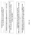
- FIG. 2B relates to a first use case. According to this use case, data is written to the cache storage area only.
- FIG. 2C which relates to a second use case (i) data is first written to the cache storage area 272 ; and (ii) at a later time, the data is copied from the cache storage area 272 to the main storage area 274 .
- FIG. 2D relating to a third use case, describes “cache bypassing.”
- data is written directly to the main storage area 274 without first being written to the cache storage area 272 .
- FIG. 3 is a flow chart describing a technique for storing data to a flash memory 270 .
- the peripheral storage device 260 receives data from host device 310 .
- this data is stored in volatile memory (for example within flash controller 280 or at any other location within non-volatile memory device 260 ).
- the data is either (i) written to cache storage area 272 before being written (if written) to main storage area 274 (use cases 1 and 2 )—i.e. the ‘first flash writing’ of the data is to cache 272 or (ii) is written to main storage area 274 without being written to cache storage area 272 (use case 3 )—i.e. the ‘first flash writing’ of the data is to the main storage area 274 .
- the ‘yes’ branch leaving step S 219 is selected, and the data is written (in step S 223 ) into the cache storage area 272 .
- the data is copied (see the optionally line leaving the box of step S 223 ) from the typically smaller cache storage area to the larger main storage area for longer-term storage. Copying the data allows the region within cache 272 in which the data was stored to be used to store new data
- the data may be written directly to main storage area 274 (according to the ‘no’ branch leaving step S 219 ) without writing the data first to the cache storage area
- flash controller 280 may be implemented using any combination of hardware (for example, including a microprocessor and optionally volatile memory such as RAM or registers), firmware and/or code-modules (for example, stored in volatile and/or non-volatile memory and executable by a microprocessor). Flash controller 280 may include any software (i.e. tangibly stored in volatile and/or non-volatile memory) and/or firmware and/or hardware element(s) including but not limited to field programmable logic array (FPLA) element(s), field programmable gate array (FPGA) element(s), and application-specific integrated circuit (ASIC) element(s). Any instruction set architecture may be used in flash controller 280 including but not limited to reduced instruction set computer (RISC) element(s) and/or complex instruction set computer (CISC).
- RISC reduced instruction set computer
- CISC complex instruction set computer
- a method of implementing a caching policy for a non-volatile storage device that has a non-volatile memory including a cache storage area and a main storage area, the method comprising: a) receiving data by the non-volatile storage device from a host device coupled to the non-volatile storage device; b) determining by the non-volatile storage device whether to write the received data to the cache storage area of the non-volatile memory before writing the received data to the main storage area of the non-volatile memory in accordance with at least one parameter selected from the group consisting of: i) a historical rate at which other data was received by the non-volatile storage device from the host device during a time period preceding the receiving of the data of step (a); and ii) an average time interval between successive host write requests received during the preceding time period; and c) in the event of a positive determining, writing the data received in step (a) to the cache storage area as determined.
- the at least one parameter includes the historical rate at which the other data was received.
- the determining to write the received data to the cache storage area of the non-volatile memory before writing the data to the main storage area is contingent upon the historical rate being above a threshold level.
- the at least one parameter includes the average time interval between successive host write requests.
- the data-receiving is carried out before the determining.
- the determining is carried out before the data-receiving.
- a method of implementing a caching policy for a non-volatile storage device that has a non-volatile memory including a cache storage area and a main storage area, the method comprising: a) receiving at least one request by the non-volatile storage device from a host device coupled to the non-volatile storage device to store data in the non-volatile memory; b) assessing a rate at which data is required to be written to the non-volatile memory in order to fulfill the at least one data storage request; c) in accordance with the assessed data-writing rate, determining whether to write the received data to the cache storage area of the non-volatile memory before writing the received data to the main storage area of the non-volatile memory; and d) in the event of a positive determining, writing the received data to the cache area as determined.
- the receiving of the at least one request includes receiving a first request and a second request; i) the rate assessing is carried out in accordance with: (A) respective amounts of data of the first and second requests; and B) a time difference between a time of receiving the first request and a time of receiving the second request.
- the receiving of the at least one request includes receiving a first request and a second request; ii) the rate assessing is carried out in accordance with a quotient between: A) the total amount of data of the first and second requests; and B) a time difference between a time of receiving the first request and a time of receiving the second request.
- a method of implementing a caching policy for a non-volatile storage device that has a non-volatile memory including a cache storage area and a main storage area, the method comprising: a) receiving a request by the non-volatile storage device from a host device coupled to the non-volatile storage device to store data in the non-volatile memory; b) if the non-volatile storage device is in a store-to-cache-first mode at a time that the request is received, write the received data to the cache storage area of the non-volatile memory before writing the received data to the main storage area of the non-volatile memory; c) if the non-volatile storage device is in a bypass-cache mode at a time that the request is received, write the received data to the main storage area of the non-volatile memory without writing the received data to the cache storage area of the non-volatile memory; and d) effecting a mode transition, by the storage device
- the method further comprises: e) in accordance with a fullness of the cache storage area, deciding whether or not to transition from the store-to-cache-first mode to the bypass-cache mode; and f) effecting the transition from the store-to-cache-first mode to the bypass-cache mode as determined.
- a method of implementing a cache flushing policy for a non-volatile storage device that has a non-volatile memory including a cache storage area and a main storage area, the method comprising: a) receiving data by the non-volatile storage device from a host device coupled to the non-volatile storage device; b) storing the received data in the cache storage area; and c) for at least one point in time: i) determining, by the non-volatile storage device, in accordance with at least one parameter selected from the group consisting of A) a historical rate at which other data was received by the non-volatile storage device from the host device during a time period preceding the receiving of the data of step (a); and B) an average time interval between successive host write requests received during the preceding time period; and whether to copy the data received in step (a) from the cache storage area of the non-volatile memory to the main storage area of the non-volatile memory; and ii) in the event of
- the at least one parameter includes the historical rate at which the other data was received.
- the at least one parameter includes the average time interval between successive host write requests.
- a non-volatile storage device comprising: a) a device interface for coupling with a host device; b) a non-volatile memory including a cache storage area and a main storage area; and c) a controller operative to: i) receive data from the host device via the device interface; ii) determine whether to write the received data to the cache storage area before writing the received data to the main storage in accordance with at least one parameter selected from the group consisting of: A) a historical rate at which other data was received by the non-volatile storage device from the host device during a time period preceding the receiving of the data of step (c)(i); and B) an average time interval between successive host write requests received during the preceding time period; and iii) in the event of a positive determining, write the data received in step (c)(i) to the cache storage area as determined.
- a non-volatile storage device comprising: a) a device interface for coupling with a host device; b) a non-volatile memory including a cache storage area and a main storage area; and c) a controller operative to: i) receive, from the host device via the device interface, at least one request to store data in the non-volatile memory; ii) assess a rate at which data is required to be written to the non-volatile memory in order to fulfill the at least one data storage request; iii) in accordance with the assessed data-writing rate, determine whether to write the received data to the cache storage area before writing the received data to the main storage area; and iv) in the event of a positive determining, write the received data to the cache storage area as determined.
- a non-volatile storage device comprising: a) a device interface for coupling with a host device; b) a non-volatile memory including a cache storage area and a main storage area; and c) a controller operative to: i) receive, from the host device via the device interface, a request to store data in the non-volatile memory; ii) if the non-volatile storage device is in a store-to-cache-first mode at a time that the request is received, write the received data to the cache storage area before writing the received data to the main storage area; iii) if the non-volatile storage device is in a bypass-cache mode at a time that the request is received, write the received data to the main storage area without writing the received data to the cache storage area of the non-volatile memory; and iv) effect a mode transition, by the storage device, from the bypass-cache mode to the store-to-cache-first mode in response
- a non-volatile storage device comprising: a) a device interface for coupling with a host device; b) a non-volatile memory including a cache storage area and a main storage area; and c) a controller operative to: i) receive data from the host device via the device interface; ii) store the received data in the cache storage area; and iii) for at least one point in time: A) determine in accordance with at least one parameter selected from the group consisting of: I) a historical rate at which other data was received by the non-volatile storage device from the host device during a time period preceding the receiving of the data of step (a); and II) an average time interval between successive host write requests received during the preceding time period; and whether to copy the data received in step c(i) from the cache storage area to the main storage area; and iv) in the event of a positive determining, copying the data received in step c(i) from the cache storage area as determined.
- FIG. 1 is a block diagram of a prior art peripheral storage device coupled to a host device.
- FIGS. 2A-2D , 3 describe prior art routines for storing data to a non-volatile memory of a peripheral storage device.
- FIG. 4 is a timeline describing information which may be utilized to enforce one or more cache-related policy(ies).
- FIGS. 5-7 , and 8 A are flow charts of routines for storing data to a non-volatile memory including a cache storage area and a main storage area.
- FIG. 8B is a flow chart of a routine for transitioning between a bypass cache mode and a store-to-cache-first mode.
- FIGS. 9-10 are flow charts of routines for enforcing a cache flushing policy.
- Some embodiments of the present invention relate to utilizing certain historical and/or predicted ‘performance data’ when deciding whether: (i) to store data to a cache storage area before storing the data to a main storage area of a non-volatile memory; or (ii) to ‘bypass’ the cache storage area by storing the data ‘directly’ in the main storage area.
- the decision of whether or not to write ‘incoming data’ to the cache storage area may be carried out in accordance with one or more of: (i) historical rates at which data has been received by a peripheral storage device from a host device (‘Parameter A’) (see FIG.
- an average time interval between successive host write requires received during a preceding time period (‘Parameter B’) (see FIG. 6 );
- an assessed data-writing rate at which data is required to be written to non-volatile memory in order to fulfill at least one data storage request (‘Parameter C’) (see FIG. 7 ); and/or (iv) one or more additional parameters described below.
- a ‘positive’ decision i.e. a decision to store the data to the cache storage area of the non-volatile memory
- the data is stored to the cache storage area as determined.
- a determining of whether or when to copy ‘cache-residing data’ (i.e. data that has already been written into the cache storage area) from the cache storage area to the main storage area may also be carried out in accordance with one or more of the aforementioned parameter(s) and/or other parameters described herein. These embodiments may be useful for determining and enforcing a ‘non-volatile cache flushing’ policy.
- peripheral storage device in the event that the peripheral storage device has recently been ‘flooded’ with a ‘large’ amount of data from the host device (i.e. data sent from the host device which needs to be stored in non-volatile storage within the peripheral storage device) in a ‘short’ period of time, then it may be assumed that there is an ‘elevated’ likelihood that in the near future, the rate at which data will be received will continue to be relatively ‘high.’
- incoming data is stored first to the cache, which is associated with a ‘faster writing speed,’ rather than directly writing to the ‘slower’ main storage region. This may be useful for minimizing the risk of a slow response time (i.e. as detectable by the host) for completing the execution of one or more write commands received from the host device.
- the rate at which data is written from the host device is historically ‘low,’ it may be preferred, when receiving data from the host device, to bypass the cache storage area and to write the received data ‘directly’ to the main storage area. In this case, refraining from storing the data to the cache storage area may be useful, for example, for minimizing the number of write operations sustained by the cache storage area of the non-volatile (for example, flash) memory, thereby extending the lifespan of cache area and/or the peripheral non-volatile storage device.
- the non-volatile for example, flash
- the rate at which data has been historically received may be indicative of an estimated rate at which data will be received from the host device in the future.
- an average time interval between successive host write-requests received during a preceding time period may be indicative of a magnitude of a workload imposed upon the peripheral storage device by the host device during the preceding time period.
- this may be indicative of (i) a situation where the host has provided many write requests in a relatively short period of time, thereby imposing a relatively ‘large’ workload upon the peripheral storage device; and (ii) an elevated likelihood that the peripheral storage device will need to handle a large workload in the future.
- the average time interval is relatively low (for example, below some threshold, pre-determined or otherwise), it may be preferred to first write incoming data received from the host device to the cache storage area, in order to minimize the risk of a slow response time (i.e. as detectable by the host) for completing the execution of one or more write commands received by the host device.
- this may be indicative of (i) a host that has been relatively ‘inactive’ in the past; and (ii) a host which has an elevated likelihood of being inactive in the future (or a reduced likelihood of being active).
- it may be preferred, when receiving data from the host device, to bypass the cache storage area and to write the received data ‘directly’ to the main storage area, despite the slower writing speed.
- refraining from storing the data to the cache storage area may be useful, for example, for minimizing the number of write operations sustained by the cache storage area of the non-volatile (for example, flash) memory, thereby extending the lifespan of cache area and/or the peripheral non-volatile storage device.
- the non-volatile for example, flash
- a rate at which data received in one or more command(s) from the host is required to be written to non-volatile memory of the peripheral non-volatile memory device is assessed.
- information describing this rate may be received explicitly from the host.
- non-volatile memory when receiving data from the host device, it may be preferred, when receiving data from the host device, to bypass the cache storage area and to write the received data ‘directly’ to the main storage area, despite the slower writing speed. In this case, refraining from storing the data to the cache storage area may be useful, for example, for minimizing the number of write operations sustained by the cache storage area of the non-volatile (for example, flash) memory, thereby extending the lifespan of cache area and/or the peripheral non-volatile storage device.
- the non-volatile for example, flash
- the decision of whether or not to write to cache before writing to main storage may be carried out “autonomously” by a peripheral non-volatile storage device, without receiving any caching instructions from the host device.
- some embodiments of the present invention relate to a technique for determining whether or when to copy ‘cache-residing data’ (i.e. data that has already been written into the cache storage area) from the cache storage area to the main storage area.
- the data is copied from the cache storage area to the main storage area contingent upon and/or in accordance with this determining.
- the determining of whether or when to copy ‘cache-residing data’ from the cache storage area may be carried out in accordance with one or more of: (i) historical rates at which data has been received by a peripheral storage device from a host device (‘Parameter A’) (see FIG. 5 ); (ii) an average time interval between successive host write requests received during a preceding time period (‘Parameter B’) (see FIG. 6 ); and/or (iiii) one or more additional parameters described below.
- the peripheral storage device in the event that the peripheral storage device has recently been ‘flooded’ with a ‘large’ amount of data from the host device (i.e. data sent from the host device which needs to be stored in non-volatile storage within the peripheral storage device) in a ‘short’ period of time, then it may be assumed that there is an ‘elevated’ likelihood that in the near future the rate at which data will be received will continue to be relatively ‘high.’ In this case, it may be advantageous to postpone flushing the cache (postpone copying data from the cache storage area to the main storage area) and/or flush the cache at a relatively ‘low rate.’ In particular, the cache copying operations whereby data is copied from the cache storage area to the main storage area may consume device resources of the peripheral non-volatile storage device, and may limit the amount of device resources available for handling “incoming data.” Thus, in the event that it is predicted that the storage device will be relatively “flooded” with new incoming data, diverting device resources to
- the rate at which data is written from the host device is historically ‘low,’ it may be preferred, when receiving data from the host device, to take advantage of the situation by dedicating device resources to the task of copying data from the cache storage area to the main storage area. Because it is anticipated that the demands placed upon the peripheral storage device by the host device will be relatively “low” in the near future, it may be assumed that the risk of the device failing to meet any of these demands will be relatively low during the time period where device resources are dedicated to copying data from the cache, providing an opportunity to “clear” the cache for new incoming data.
- an average time interval between successive host write-requests received during a preceding time period is indicative of how ‘active’ the host device has been in sending commands or specific tasks to the peripheral storage device.
- this may be indicative of (i) a situation where the host has provided many write requests in a relatively short period of time, thereby imposing a relatively ‘large’ workload upon the peripheral storage device; and (ii) an elevated likelihood that the peripheral storage device will need to handle a large workload in the future.
- the cache copying operations whereby data is copied from the cache storage area to the main storage area may consume device resources of the peripheral non-volatile storage device, and may limit the amount of device resources available for handling “incoming data.”
- diverting device resources to cache flushing may increase the risk that the peripheral storage device will not be able to “handle” the incoming data (i.e. as detectable by the host device) at the rate required and/or required.
- the decision of whether or not (or when) to copy ‘cache-residing data’ from the cache area to the main area may be carried out “autonomously” by a peripheral flash device, without receiving any caching instructions from the host device.
- FIG. 4 is a timeline describing information which may be utilized to enforce one or more cache-related policy(ies).
- a first “write request” including data D 1 is received at peripheral storage device 260 from host device 310 via respective interfaces 350 , 250 .
- a second “write request” including data D 2 is received at peripheral storage device 260 from host device 310 via respective interfaces 350 , 250 .
- a third “write request” including data D 3 is received at peripheral storage device 260 from host device 310 via respective interfaces 350 , 250 .
- a fourth “write request” including data D 4 is received at peripheral storage device 260 from host device 310 via respective interfaces 350 , 250 .
- a fifth “write request” including data D 5 is received at peripheral storage device 260 from host device 310 via respective interfaces 350 , 250 .
- the “time gap” between (i) the receiving of data D 2 /the receiving of the second write request and (ii) the receiving of data of D 1 /the receiving of the first write request is ⁇ t 12 .
- the “time gap” between (i) the receiving of data D 3 //the receiving of the third write request and (ii) the receiving of data of D 2 /the receiving of the second write request is ⁇ t 23 .
- the “time gap” between (i) the receiving of data D 4 /the receiving of the fourth write request and (ii) the receiving of data of D 3 /the receiving of the third write request is ⁇ t 34 .
- the “time gap” between (i) the receiving of data D 5 /the receiving of the fifth write request and (ii) the receiving of data of D 4 /the receiving of the fourth write request is ⁇ t 45 .
- FIG. 5 is a flow chart describing a technique for storing data to a flash memory 270 .
- the peripheral storage device 260 receives data from host device 310 .
- this data is stored in volatile memory (for example within flash controller 280 or at any other location within non-volatile memory device 260 ).
- step S 251 a historical rate at which other data was received during a time period preceding the receiving of data in step S 211 is assessed or determined.
- step S 211 is carried out at time t 4 as part of receiving command 4 .
- the “data” received is D 4 .
- the preceding time period begins at time t 2 ⁇ t 12 and ends at time t 3 + ⁇ t 34 .
- the total “length” of the preceding time interval is (t 3 + ⁇ t 34 ) ⁇ (t 2 ⁇ t 12 , and the total amount of “other data” received during the “preceding time interval” (i.e. which preceded time t 4 ) is (D 2 +D 3 ).
- the ‘historical rate’ R at which the “other data” is received during the “historical time period” is
- step S 255 it is determined in accordance with the historical data receiving rate R if the data will be cached.
- R is compared with some sort of threshold (for example, a predetermined threshold value and/or a threshold value which changes as a function of time and/or any other threshold value): (i) in the event that R exceeds the threshold, the “yes” branch leaving S 219 is taken; and (ii) otherwise, the “no” branch leaving 5219 is taken.
- some sort of threshold for example, a predetermined threshold value and/or a threshold value which changes as a function of time and/or any other threshold value
- FIG. 6 is a flow chart describing a technique for storing data to a flash memory 270 .
- the peripheral storage device 260 receives data from host device 310 .
- this data is stored in volatile memory (for example within flash controller 280 or at any other location within non-volatile memory device 260 ).
- step S 261 an average time interval between successive host write requests during a time period preceding the receiving of data in step S 211 is assessed or determined.
- step S 211 is carried out at time t 5 as part of receiving command 5 .
- the preceding time period begins at time t 2 ⁇ t 12 and ends at time t 4 + ⁇ t 45 .
- three host write requests are received: the second write request at time t 2 , the third write request at time t 3 , and the fourth write request at time t 4 .
- the average time interval between successive host write requests T AVG is
- step S 265 it is determined in accordance with the average time interval between successive host write requests T AVG if the data will be cached.
- T AVG is compared with some sort of threshold (for example, a predetermined threshold value and/or a threshold value which changes as a function of time and/or any other threshold value): (i) in the event that T AVG is less than the threshold, the “yes” branch leaving 5219 is taken; and (ii) otherwise, the “no” branch leaving S 219 is taken.
- some sort of threshold for example, a predetermined threshold value and/or a threshold value which changes as a function of time and/or any other threshold value
- FIG. 7 is a flow chart describing a technique for storing data to a flash memory 270 .
- the peripheral storage device 260 receives data from host device 310 .
- this data is stored in volatile memory (for example within flash controller 280 or at any other location within non-volatile memory device 260 ).
- step S 315 a rate at which data received in step S 311 is required to be written to non-volatile memory to fulfill the at least one data storage request may be assessed.
- this information may be received explicitly—for example, the command set of the peripheral storage device may include a write command with a syntax where the host device requests that a certain amount of data be stored within a certain amount of time.
- the rate at which data is required to be written may then be considered to be a function of (i) the amount of data received from the host device in the particular command; and (ii) the amount of time in which the data is to be written, according to the request from the host device.
- historical patterns may be used to estimate a rate in which data is required to be written to non-volatile memory.
- step S 319 it is determined in accordance with the assessed rate AR at which data is required to be written if the data will be cached.
- AR is compared with some sort of threshold (for example, a predetermined threshold value and/or a threshold value which changes as a function of time and/or any other threshold value): (i) in the event that AR is greater than the threshold (i.e. requiring that data is written relatively quickly), the “yes” branch leaving S 219 is taken; and (ii) otherwise, the “no” branch leaving S 219 is taken.
- some sort of threshold for example, a predetermined threshold value and/or a threshold value which changes as a function of time and/or any other threshold value
- FIGS. 8A-8B if the host reads a storage ready/busy flag (i.e. of the peripheral storage device 260 ) that returned a busy status, this may be indicative that the peripheral storage device is not successfully writing data to non-volatile storage at the rate “desired” by the host device. In this case, in order to provide “better performance” for the host device, it may be desirable to first write incoming data to the cache storage area, utilizing the “fast writing” property provided by the cache storage area.
- a storage ready/busy flag i.e. of the peripheral storage device 260
- this may be indicative that the peripheral storage device is not successfully writing data to non-volatile storage at the rate “desired” by the host device.
- FIG. 8A is a flow chart describing a technique for storing data to a flash memory 270 .
- peripheral storage device 260 provides at least two device “modes”: a first mode referred to as the “store-to-cache-first” device mode whereby data is stored in the cache storage area 272 before being written to the main storage area 274 , and a second mode referred to as “bypass-cache mode” whereby data is stored in the main storage area 274 without being written to the cache storage area 272 .
- Information about a “current mode” may be stored in any location, including but not limited to flash controller 280 , volatile memory 282 and flash memory 270 .
- step S 211 of FIG. 8A the peripheral storage device 260 receives data from host device 310 .
- this data is stored in volatile memory (for example within flash controller 280 or at any other location within non-volatile memory device 260 ).
- FIG. 8B is a flow chart of routine for transitioning between the two aforementioned device modes.
- the device may transition from the “bypass cache mode” to the store-to-cache-first mode in response to a reading, by the host, of a storage ready/busy flag (i.e. the host queries the peripheral storage device of its status, and the peripheral storage device returns a storage ready/busy flag to the host device which is read by the host device).
- a storage ready/busy flag i.e. the host queries the peripheral storage device of its status, and the peripheral storage device returns a storage ready/busy flag to the host device which is read by the host device.
- peripheral storage device 260 effects a transition back to bypass cache mode in accordance with one or more events.
- this transition in accordance with a “fullness” of the cache storage area (i.e. how full the cache area is 272 with previously-written data)—for example, if the cache is close to “full” it may be advisable to effect the transition from the store-to-cache-first mode to a bypass cache mode, since there is not enough space in the cache to write incoming data into the flash.
- step S 271 of FIG. 8A it is noted that: (i) in the event that peripheral device 260 is in “store-to-cache-first” mode, the “left” branch leaving step S 271 is taken; and (ii) otherwise, the “right” branch leaving step S 271 is taken.
- FIGS. 5-8 describe routines for implementing a policy for storing incoming data to non-volatile memory 270 of a peripheral storage device 260 .
- FIG. 9-10 describe routines for copying data from a cache storage area 270 of a non-volatile memory to a main storage area 274 (see the earlier section entitled “An Introductory Discussion of Techniques for Copying Data from a Cache Storage Area of Non-Volatile Memory of a Peripheral Non-Volatile Memory Storage Device to a Main Storage Area”).
- step S 511 the peripheral storage device 260 receives data from host device 310 .
- this data is stored in the cache storage area 272 of non-volatile memory 270 .
- step S 519 an historical rate at which other data was received during a time period preceding the receiving of data in step S 511 is determined (see step S 251 of FIG. 5 ).
- step S 523 it is determined, in accordance with the historical data receiving rate, if data will be copied (i.e. at a particular time or in a particular time frame or at any time) from the cache storage area 272 to the main storage area 274 .
- step S 523 if step S 523 yielded a “positive determining” (i.e. a determining that data will be copied from the cache storage area 272 to the main storage area 274 ), then data is copied from the cache storage area 272 to the main storage area 274 as determined.
- a “positive determining” i.e. a determining that data will be copied from the cache storage area 272 to the main storage area 274
- any of the step(s) of FIG. 9 may be repeated any number of times.
- the historical rate at which data was received may be monitored (for example, at a plurality of points in time), and in response to an increase (or decrease) of the historical rate (which itself may fluctuate in time), data may be copied from the cache storage area 272 to the main storage area 274 , or a process in which data is being copied from cache storage area 272 to the main storage area 274 may cease.
- step S 511 the peripheral storage device 260 receives data from host device 310 .
- this data is stored in the cache storage area 272 of non-volatile memory 270 .
- step S 519 a magnitude of an average time interval between successive host write requests sent form host 310 to peripheral storage device 260 during a historical time period preceding the receiving of data in step S 511 is determined (see step S 261 of FIG. 6 ).
- step S 531 it is determined, in accordance with the magnitude of the average time interval, if data will be copied (i.e. at a particular time or in a particular time frame or at any time) from the cache storage area 272 to the main storage area 274 .
- step S 535 if step S 523 yielded a “positive determining” (i.e. a determining that data will be copied from the cache storage area 272 to the main storage area 274 ), then data is copied from the cache storage area 272 to the main storage area 274 as determined.
- a “positive determining” i.e. a determining that data will be copied from the cache storage area 272 to the main storage area 274
- any of the step(s) of FIG. 10 may be repeated any number of times.
- the average time interval between successive host write requests may be monitored (for example, at a plurality of points in time), and in response to an increase (or decrease) of the historical rate (which itself may fluctuate in time), data may be copied from the cache storage area 272 to the main storage area 274 , or a process in which data is being copied from cache storage area 272 to the main storage area 274 may cease.
- Non-volatile memory refers to any kind of non-volatile memory including flash memory and magnetic memory.
- “Incoming data” refers to data received by a flash memory device from a host that has not yet been stored in non-volatile memory (for example, flash memory) of the flash memory device. “Incoming data” may be temporarily stored (for example, by flash controller 280 ) in volatile memory 270 within the flash memory device.
- an “extent to which the cache storage area 272 is full of previously-stored data” is determined.
- “Previously-stored data” refers to data stored in cache storage area 272 of non-volatile memory 270 before the time at which the “extent to which the flash memory storage device is full of previously-stored data” is determined.
- any of the embodiments described above may further include receiving, sending or storing instructions and/or data that implement the operations described above in conjunction with the figures upon a computer readable medium.
- a computer readable medium may include storage media or memory media such as magnetic or flash or optical media, e.g. disk or CD-ROM, volatile or non-volatile media such as RAM, ROM, etc. as well as transmission media or signals such as electrical, electromagnetic or digital signals conveyed via a communication medium such as network and/or wireless links.
Abstract
Description
Claims (14)
Priority Applications (6)
| Application Number | Priority Date | Filing Date | Title |
|---|---|---|---|
| US12/430,089 US8103822B2 (en) | 2009-04-26 | 2009-04-26 | Method and apparatus for implementing a caching policy for non-volatile memory |
| KR1020117027816A KR101201922B1 (en) | 2009-04-26 | 2010-04-17 | Method and apparatus for implementing a caching policy for non-volatile memory |
| JP2012507833A JP2012524952A (en) | 2009-04-26 | 2010-04-17 | Method and apparatus for implementing a caching policy for non-volatile memory |
| PCT/IB2010/000858 WO2010125436A1 (en) | 2009-04-26 | 2010-04-17 | Method and apparatus for implementing a caching policy for non-volatile memory |
| EP10717755.2A EP2425345B1 (en) | 2009-04-26 | 2010-04-17 | Method and apparatus for implementing a caching policy for non-volatile memory |
| TW099113201A TW201109919A (en) | 2009-04-26 | 2010-04-26 | Method and apparatus for implementing a caching policy for non-volatile memory |
Applications Claiming Priority (1)
| Application Number | Priority Date | Filing Date | Title |
|---|---|---|---|
| US12/430,089 US8103822B2 (en) | 2009-04-26 | 2009-04-26 | Method and apparatus for implementing a caching policy for non-volatile memory |
Publications (2)
| Publication Number | Publication Date |
|---|---|
| US20100274962A1 US20100274962A1 (en) | 2010-10-28 |
| US8103822B2 true US8103822B2 (en) | 2012-01-24 |
Family
ID=42288835
Family Applications (1)
| Application Number | Title | Priority Date | Filing Date |
|---|---|---|---|
| US12/430,089 Active 2030-07-20 US8103822B2 (en) | 2009-04-26 | 2009-04-26 | Method and apparatus for implementing a caching policy for non-volatile memory |
Country Status (6)
| Country | Link |
|---|---|
| US (1) | US8103822B2 (en) |
| EP (1) | EP2425345B1 (en) |
| JP (1) | JP2012524952A (en) |
| KR (1) | KR101201922B1 (en) |
| TW (1) | TW201109919A (en) |
| WO (1) | WO2010125436A1 (en) |
Cited By (2)
| Publication number | Priority date | Publication date | Assignee | Title |
|---|---|---|---|---|
| US10339053B2 (en) | 2016-12-09 | 2019-07-02 | Hewlett Packard Enterprise Development Lp | Variable cache flushing |
| US10417736B2 (en) | 2016-05-11 | 2019-09-17 | Samsung Electronics Co., Ltd. | Graphics processing unit and method of controlling cache bypass thereof |
Families Citing this family (49)
| Publication number | Priority date | Publication date | Assignee | Title |
|---|---|---|---|---|
| US10430338B2 (en) | 2008-09-19 | 2019-10-01 | Oracle International Corporation | Selectively reading data from cache and primary storage based on whether cache is overloaded |
| EP2350875A1 (en) | 2008-09-19 | 2011-08-03 | Oracle International Corporation | Storage-side storage request management |
| US8868831B2 (en) | 2009-09-14 | 2014-10-21 | Oracle International Corporation | Caching data between a database server and a storage system |
| US8499120B2 (en) * | 2008-10-17 | 2013-07-30 | Seagate Technology Llc | User selectable caching management |
| KR20110019891A (en) * | 2009-08-21 | 2011-03-02 | 삼성전자주식회사 | Remote date back-up method and remote data back-up system |
| US8566531B2 (en) | 2009-08-21 | 2013-10-22 | Google Inc. | System and method of selectively caching information based on the interarrival time of requests for the same information |
| US8924645B2 (en) * | 2010-03-08 | 2014-12-30 | Hewlett-Packard Development Company, L. P. | Data storage apparatus and methods |
| JP5434738B2 (en) * | 2010-03-26 | 2014-03-05 | 日本電気株式会社 | Disk unit |
| US8402226B1 (en) * | 2010-06-18 | 2013-03-19 | Emc Corporation | Rate proportional cache write-back in a storage server |
| US8639887B2 (en) * | 2010-06-23 | 2014-01-28 | International Business Machines Corporation | Dynamically altering a pipeline controller mode based on resource availability |
| US8635409B2 (en) | 2010-06-23 | 2014-01-21 | International Business Machines Corporation | Dynamic mode transitions for cache instructions |
| US9213628B2 (en) * | 2010-07-14 | 2015-12-15 | Nimble Storage, Inc. | Methods and systems for reducing churn in flash-based cache |
| US9977732B1 (en) * | 2011-01-04 | 2018-05-22 | Seagate Technology Llc | Selective nonvolatile data caching based on estimated resource usage |
| US8630418B2 (en) * | 2011-01-05 | 2014-01-14 | International Business Machines Corporation | Secure management of keys in a key repository |
| US8788742B2 (en) * | 2011-05-23 | 2014-07-22 | International Business Machines Corporation | Using an attribute of a write request to determine where to cache data in a storage system having multiple caches including non-volatile storage cache in a sequential access storage device |
| US8984225B2 (en) * | 2011-06-22 | 2015-03-17 | Avago Technologies General Ip (Singapore) Pte. Ltd. | Method to improve the performance of a read ahead cache process in a storage array |
| US9378142B2 (en) | 2011-09-30 | 2016-06-28 | Intel Corporation | Apparatus and method for implementing a multi-level memory hierarchy having different operating modes |
| US10592416B2 (en) | 2011-09-30 | 2020-03-17 | Oracle International Corporation | Write-back storage cache based on fast persistent memory |
| JP2013090006A (en) * | 2011-10-13 | 2013-05-13 | Nikon Corp | Electronic apparatus and program |
| US10681394B2 (en) | 2011-11-28 | 2020-06-09 | Comcast Cable Communications, Llc | Cache eviction during off-peak transaction time period |
| US20130151755A1 (en) | 2011-12-12 | 2013-06-13 | Reuven Elhamias | Non-Volatile Storage Systems with Go To Sleep Adaption |
| US10073656B2 (en) | 2012-01-27 | 2018-09-11 | Sandisk Technologies Llc | Systems and methods for storage virtualization |
| US10359972B2 (en) * | 2012-08-31 | 2019-07-23 | Sandisk Technologies Llc | Systems, methods, and interfaces for adaptive persistence |
| US9659041B2 (en) * | 2012-01-30 | 2017-05-23 | Oracle International Corporation | Model for capturing audit trail data with reduced probability of loss of critical data |
| US8996818B2 (en) * | 2012-12-09 | 2015-03-31 | Advanced Micro Devices, Inc. | Bypassing memory requests to a main memory |
| US9058282B2 (en) | 2012-12-31 | 2015-06-16 | Intel Corporation | Dynamic cache write policy |
| US9170943B2 (en) * | 2013-08-29 | 2015-10-27 | Globalfoundries U.S. 2 Llc | Selectively enabling write caching in a storage system based on performance metrics |
| US10229161B2 (en) | 2013-09-20 | 2019-03-12 | Oracle International Corporation | Automatic caching of scan and random access data in computing systems |
| US9411721B2 (en) | 2013-11-15 | 2016-08-09 | Sandisk Technologies Llc | Detecting access sequences for data compression on non-volatile memory devices |
| JP6289883B2 (en) * | 2013-11-27 | 2018-03-07 | 株式会社東芝 | Storage device |
| KR102303008B1 (en) * | 2014-08-15 | 2021-09-15 | 마이크로소프트 테크놀로지 라이센싱, 엘엘씨 | Flushing in file system |
| US10095628B2 (en) | 2015-09-29 | 2018-10-09 | International Business Machines Corporation | Considering a density of tracks to destage in groups of tracks to select groups of tracks to destage |
| US10241918B2 (en) * | 2015-09-29 | 2019-03-26 | International Business Machines Corporation | Considering a frequency of access to groups of tracks to select groups of tracks to destage |
| US10120811B2 (en) | 2015-09-29 | 2018-11-06 | International Business Machines Corporation | Considering a frequency of access to groups of tracks and density of the groups to select groups of tracks to destage |
| WO2017111891A1 (en) * | 2015-12-21 | 2017-06-29 | Hewlett Packard Enterprise Development Lp | Caching io requests |
| US10133667B2 (en) | 2016-09-06 | 2018-11-20 | Orcle International Corporation | Efficient data storage and retrieval using a heterogeneous main memory |
| US10078591B2 (en) * | 2016-09-27 | 2018-09-18 | International Business Machines Corporation | Data storage cache management |
| US10331573B2 (en) | 2016-11-04 | 2019-06-25 | Oracle International Corporation | Detection of avoidable cache thrashing for OLTP and DW workloads |
| JP2018106573A (en) * | 2016-12-28 | 2018-07-05 | 富士通株式会社 | Storage control apparatus and control program |
| US10803039B2 (en) | 2017-05-26 | 2020-10-13 | Oracle International Corporation | Method for efficient primary key based queries using atomic RDMA reads on cache friendly in-memory hash index |
| US10719446B2 (en) | 2017-08-31 | 2020-07-21 | Oracle International Corporation | Directly mapped buffer cache on non-volatile memory |
| US11086876B2 (en) | 2017-09-29 | 2021-08-10 | Oracle International Corporation | Storing derived summaries on persistent memory of a storage device |
| US10802766B2 (en) | 2017-09-29 | 2020-10-13 | Oracle International Corporation | Database with NVDIMM as persistent storage |
| US10732836B2 (en) | 2017-09-29 | 2020-08-04 | Oracle International Corporation | Remote one-sided persistent writes |
| US10956335B2 (en) | 2017-09-29 | 2021-03-23 | Oracle International Corporation | Non-volatile cache access using RDMA |
| JP2020035128A (en) * | 2018-08-29 | 2020-03-05 | キオクシア株式会社 | Memory system |
| JP7118827B2 (en) * | 2018-09-12 | 2022-08-16 | 株式会社東芝 | Information processing device, memory control method and program |
| KR102605566B1 (en) | 2018-11-22 | 2023-11-24 | 에스케이하이닉스 주식회사 | Memory controller and operating method thereof |
| KR102343599B1 (en) * | 2020-12-23 | 2021-12-27 | 주식회사 파두 | Memory controller and storage device including the same |
Citations (14)
| Publication number | Priority date | Publication date | Assignee | Title |
|---|---|---|---|---|
| US6263398B1 (en) * | 1998-02-10 | 2001-07-17 | Ramtron International Corporation | Integrated circuit memory device incorporating a non-volatile memory array and a relatively faster access time memory cache |
| US6496905B1 (en) | 1999-10-01 | 2002-12-17 | Hitachi, Ltd. | Write buffer with burst capability |
| US20040117441A1 (en) | 2002-12-09 | 2004-06-17 | Infabric Technologies, Inc. | Data-aware data flow manager |
| US20040128470A1 (en) | 2002-12-27 | 2004-07-01 | Hetzler Steven Robert | Log-structured write cache for data storage devices and systems |
| US20050066121A1 (en) | 2003-09-24 | 2005-03-24 | Keeler Stanton M. | Multi-level caching in data storage devices |
| US20050193025A1 (en) | 2004-03-01 | 2005-09-01 | M-Systems Flash Disk Pioneers, Ltd. | File system that manages files according to content |
| US20050256838A1 (en) | 2004-05-17 | 2005-11-17 | M-Systems Flash Disk Pioneers, Ltd. | Method of managing files for optimal performance |
| US20070016725A1 (en) | 2005-07-14 | 2007-01-18 | Chu Frank R | System and method for selective write to flash memory in HDD |
| US20070106842A1 (en) | 2005-11-04 | 2007-05-10 | Conley Kevin M | Enhanced first level storage caching methods using nonvolatile memory |
| US20070113000A1 (en) | 2005-11-15 | 2007-05-17 | M-Systems Flash Disk Pioneers Ltd. | Flash memory device and method |
| US20070276989A1 (en) | 2006-05-29 | 2007-11-29 | Sandisk Il Ltd. | Predictive data-loader |
| US20070283081A1 (en) | 2006-06-06 | 2007-12-06 | Msystem Ltd. | Cache control in a non-volatile memory device |
| US20080209109A1 (en) | 2007-02-25 | 2008-08-28 | Sandisk Il Ltd. | Interruptible cache flushing in flash memory systems |
| US7793061B1 (en) * | 2007-06-29 | 2010-09-07 | Emc Corporation | Techniques for using flash-based memory as a write cache and a vault |
-
2009
- 2009-04-26 US US12/430,089 patent/US8103822B2/en active Active
-
2010
- 2010-04-17 KR KR1020117027816A patent/KR101201922B1/en not_active IP Right Cessation
- 2010-04-17 EP EP10717755.2A patent/EP2425345B1/en not_active Not-in-force
- 2010-04-17 WO PCT/IB2010/000858 patent/WO2010125436A1/en active Application Filing
- 2010-04-17 JP JP2012507833A patent/JP2012524952A/en active Pending
- 2010-04-26 TW TW099113201A patent/TW201109919A/en unknown
Patent Citations (15)
| Publication number | Priority date | Publication date | Assignee | Title |
|---|---|---|---|---|
| US6263398B1 (en) * | 1998-02-10 | 2001-07-17 | Ramtron International Corporation | Integrated circuit memory device incorporating a non-volatile memory array and a relatively faster access time memory cache |
| US6496905B1 (en) | 1999-10-01 | 2002-12-17 | Hitachi, Ltd. | Write buffer with burst capability |
| US20040117441A1 (en) | 2002-12-09 | 2004-06-17 | Infabric Technologies, Inc. | Data-aware data flow manager |
| US20040128470A1 (en) | 2002-12-27 | 2004-07-01 | Hetzler Steven Robert | Log-structured write cache for data storage devices and systems |
| US20050066121A1 (en) | 2003-09-24 | 2005-03-24 | Keeler Stanton M. | Multi-level caching in data storage devices |
| US20050193025A1 (en) | 2004-03-01 | 2005-09-01 | M-Systems Flash Disk Pioneers, Ltd. | File system that manages files according to content |
| US20050256838A1 (en) | 2004-05-17 | 2005-11-17 | M-Systems Flash Disk Pioneers, Ltd. | Method of managing files for optimal performance |
| US20070016725A1 (en) | 2005-07-14 | 2007-01-18 | Chu Frank R | System and method for selective write to flash memory in HDD |
| US20070106842A1 (en) | 2005-11-04 | 2007-05-10 | Conley Kevin M | Enhanced first level storage caching methods using nonvolatile memory |
| US20070113000A1 (en) | 2005-11-15 | 2007-05-17 | M-Systems Flash Disk Pioneers Ltd. | Flash memory device and method |
| US20070276989A1 (en) | 2006-05-29 | 2007-11-29 | Sandisk Il Ltd. | Predictive data-loader |
| US20070276990A1 (en) | 2006-05-29 | 2007-11-29 | Sandisk Il Ltd. | Method for preloading data to improve data-retrieval times |
| US20070283081A1 (en) | 2006-06-06 | 2007-12-06 | Msystem Ltd. | Cache control in a non-volatile memory device |
| US20080209109A1 (en) | 2007-02-25 | 2008-08-28 | Sandisk Il Ltd. | Interruptible cache flushing in flash memory systems |
| US7793061B1 (en) * | 2007-06-29 | 2010-09-07 | Emc Corporation | Techniques for using flash-based memory as a write cache and a vault |
Cited By (2)
| Publication number | Priority date | Publication date | Assignee | Title |
|---|---|---|---|---|
| US10417736B2 (en) | 2016-05-11 | 2019-09-17 | Samsung Electronics Co., Ltd. | Graphics processing unit and method of controlling cache bypass thereof |
| US10339053B2 (en) | 2016-12-09 | 2019-07-02 | Hewlett Packard Enterprise Development Lp | Variable cache flushing |
Also Published As
| Publication number | Publication date |
|---|---|
| WO2010125436A1 (en) | 2010-11-04 |
| EP2425345A1 (en) | 2012-03-07 |
| EP2425345B1 (en) | 2013-10-23 |
| KR20120002547A (en) | 2012-01-05 |
| US20100274962A1 (en) | 2010-10-28 |
| TW201109919A (en) | 2011-03-16 |
| KR101201922B1 (en) | 2012-11-15 |
| JP2012524952A (en) | 2012-10-18 |
Similar Documents
| Publication | Publication Date | Title |
|---|---|---|
| US8103822B2 (en) | Method and apparatus for implementing a caching policy for non-volatile memory | |
| US11204696B2 (en) | Memory devices and electronic systems having a hybrid cache including static and dynamic caches that may be selectively disabled based on cache workload or availability, and related methods | |
| KR102345927B1 (en) | Managed NVM Adaptive Cache Management | |
| TWI539277B (en) | System, method and computer program product for increasing spare space in memory to extend a lifetime of the memory | |
| US9256542B1 (en) | Adaptive intelligent storage controller and associated methods | |
| CN102648457B (en) | Mixing storage is used to extend SSD life cycle | |
| TWI474335B (en) | System, method, and computer program product for increasing a lifetime of a plurality of blocks of memory | |
| US8327076B2 (en) | Systems and methods of tiered caching | |
| KR101861545B1 (en) | Method for managing data in storage device | |
| US20130060994A1 (en) | Non-volatile memory management system with time measure mechanism and method of operation thereof | |
| US20170286289A1 (en) | Data storage device and flash memory control method | |
| US20090193182A1 (en) | Information storage device and control method thereof | |
| JP5814335B2 (en) | Reduction of writing and estimation and display of remaining life of nonvolatile memory | |
| TW201333696A (en) | Method, non-transistory computer readable medium and apparatus for writing data to different portions of memory based on write frequency | |
| US20180018224A1 (en) | Method for managing data stored in flash memory and associated memory device and controller | |
| TW201227739A (en) | Method for performing block management, and associated memory device and controller thereof | |
| US20100241792A1 (en) | Storage device and method of managing a buffer memory of the storage device | |
| US20160098213A1 (en) | Hybrid storage system employing reconfigurable memory | |
| US20150127886A1 (en) | Memory system and method | |
| WO2009031727A1 (en) | Cache management method and cache device using sector set | |
| CN109690465B (en) | Storage device management method and user terminal | |
| US8234418B1 (en) | Periodic and conditional execution of DMA operations | |
| KR101718888B1 (en) | Memory system and garbage collection method thereof |
Legal Events
| Date | Code | Title | Description |
|---|---|---|---|
| AS | Assignment |
Owner name: SANDISK IL LTD., AN ISRAELI CORPORATION, ISRAEL Free format text: ASSIGNMENT OF ASSIGNORS INTEREST;ASSIGNORS:LASSER, MENAHEM;MURIN, MARK;REEL/FRAME:023380/0889 Effective date: 20090609 |
|
| AS | Assignment |
Owner name: SANDISK IL LTD., AN ISRAELI CORPORATION, ISRAEL Free format text: EMPLOYMENT AGREEMENT;ASSIGNOR:MOSEK, AMIR;REEL/FRAME:023395/0587 Effective date: 19981208 |
|
| STCF | Information on status: patent grant |
Free format text: PATENTED CASE |
|
| FPAY | Fee payment |
Year of fee payment: 4 |
|
| MAFP | Maintenance fee payment |
Free format text: PAYMENT OF MAINTENANCE FEE, 8TH YEAR, LARGE ENTITY (ORIGINAL EVENT CODE: M1552); ENTITY STATUS OF PATENT OWNER: LARGE ENTITY Year of fee payment: 8 |
|
| AS | Assignment |
Owner name: WESTERN DIGITAL ISRAEL LTD, ISRAEL Free format text: CHANGE OF NAME;ASSIGNOR:SANDISK IL LTD;REEL/FRAME:053574/0513 Effective date: 20191112 |
|
| MAFP | Maintenance fee payment |
Free format text: PAYMENT OF MAINTENANCE FEE, 12TH YEAR, LARGE ENTITY (ORIGINAL EVENT CODE: M1553); ENTITY STATUS OF PATENT OWNER: LARGE ENTITY Year of fee payment: 12 |