US8103988B2 - Use of breakouts in printed circuit board designs - Google Patents
Use of breakouts in printed circuit board designs Download PDFInfo
- Publication number
- US8103988B2 US8103988B2 US11/937,411 US93741107A US8103988B2 US 8103988 B2 US8103988 B2 US 8103988B2 US 93741107 A US93741107 A US 93741107A US 8103988 B2 US8103988 B2 US 8103988B2
- Authority
- US
- United States
- Prior art keywords
- escape
- pins
- pseudo
- pin
- traces
- Prior art date
- Legal status (The legal status is an assumption and is not a legal conclusion. Google has not performed a legal analysis and makes no representation as to the accuracy of the status listed.)
- Active
Links
Images


Classifications
-
- G—PHYSICS
- G06—COMPUTING; CALCULATING OR COUNTING
- G06F—ELECTRIC DIGITAL DATA PROCESSING
- G06F30/00—Computer-aided design [CAD]
- G06F30/30—Circuit design
- G06F30/39—Circuit design at the physical level
-
- H—ELECTRICITY
- H05—ELECTRIC TECHNIQUES NOT OTHERWISE PROVIDED FOR
- H05K—PRINTED CIRCUITS; CASINGS OR CONSTRUCTIONAL DETAILS OF ELECTRIC APPARATUS; MANUFACTURE OF ASSEMBLAGES OF ELECTRICAL COMPONENTS
- H05K1/00—Printed circuits
- H05K1/02—Details
- H05K1/11—Printed elements for providing electric connections to or between printed circuits
- H05K1/111—Pads for surface mounting, e.g. lay-out
- H05K1/112—Pads for surface mounting, e.g. lay-out directly combined with via connections
-
- H—ELECTRICITY
- H05—ELECTRIC TECHNIQUES NOT OTHERWISE PROVIDED FOR
- H05K—PRINTED CIRCUITS; CASINGS OR CONSTRUCTIONAL DETAILS OF ELECTRIC APPARATUS; MANUFACTURE OF ASSEMBLAGES OF ELECTRICAL COMPONENTS
- H05K3/00—Apparatus or processes for manufacturing printed circuits
- H05K3/0005—Apparatus or processes for manufacturing printed circuits for designing circuits by computer
Definitions
- the present invention is directed to improving the use of breakouts during the design of a printed circuit board.
- Various implementations of the invention may be useful for routing escape traces of breakouts.
- Other implementations of the invention may alternately or additionally be employed to improve the routability of traces from breakouts in a printed circuit board design.
- Integrated circuit devices are used in a wide variety of modern appliances, such as computers, automobiles, telephones, televisions, manufacturing tools, satellites and even toys. While even a small integrated circuit device can provide a great deal of functionality, almost every integrated circuit device must be electrically connected to an input or output device, to another integrated circuit device, or to some other electronic component in order to be useful. To provide these electrical connections, integrated circuit devices are typically mounted on a printed circuit board (PCB). Most printed circuit boards have a rigid, planar core. The core may be formed, for example, of a sheet of fiberglass material impregnated with epoxy. Conductive lines or “traces” then are formed on one or both surfaces of the core, to electronically connect the components attached to the printed circuit board. The traces may be formed of any desired conductive material, such as copper. With various manufacturing techniques, material, specific traces may be created by etching a single layer of conductive material in a photolithographic process.
- Simple printed circuit boards may have only a single core, with traces on one or both sides of the core. More complex printed circuit boards, however, may have multiple cores, with traces on one or both sides of one or more of the cores. These multilayered printed circuit board also may include layers of insulating material, to prevent traces on adjacent core surfaces from contacting. In addition, a multilayered printed circuit board also will include one or more “vias” to electrically connect two or more different layers of the board. A via is created by drilling or otherwise forming a hole through one or more cores. The walls of the via then may be clad with conductive material to form an electrical connection between the different layers. Alternately or additionally, the entire via may be filled with conductive material to form the electrical connection.
- Some vias will pass through every layer of the board, while other vias may connect only some of the layers in the board. Some vias, referred to as “blind” vias, will connect only internal layers of the board, and are not connected to either the uppermost or lowermost layers. As will be explained in more detail below, vias are employed where, for example, a component requires more traces than can be routed in a corresponding area of a single board layer. The vias allow the component to connect to traces on other layers of the board.
- a designer will create a schematic diagram for the system to be connected through the printed circuit board. This process includes identifying each component that will be included in the system.
- a system can include “active” components, such as field programmable gate array (FPGA) integrated circuits or application-specific integrated circuits (ASICs).
- a system also can include “passive” components, such as connectors formed as an integrated circuit, resistors, capacitors, and inductors.
- the schematic design will represent the electrical connections that must be formed between each component.
- a designer typically will verify the functionality of the system described in the schematic design. The design may, for example, use software modeling tools to ensure that the system described in the schematic will reliably perform the desired operations. If any errors are detected, then the schematic design will be corrected to address the errors, and the functional verification process repeated.
- the designer will create a physical design to implement the schematic design.
- the designer will begin by selecting a physical location in the design for each component.
- the designer will add a component object, representing that component, to that location in the printed circuit board design.
- the component object may include a variety of information regarding the physical component it represents, such as the configuration of the connection pins used to electrically connect that component to other components.
- the substrate with the integrated circuit will be encased in a package for protection from the environment.
- the pins serve to provide an electrical connection, through the packaging, to the electrical contacts of the integrated circuit.
- a component's minimum current requirement may require that the trace supplying that current have a minimum width.
- traces may require a minimum separation distance to prevent unacceptable crosstalk.
- Timing constraints may limit the length and/or impedance of a trace.
- connections between component pins may require routing traces on multiple layers of the printed circuit board.
- a designer may revise it several times before it is finished. These revisions may include, for example, moving the pathways for traces, altering the width of traces at various points along their lengths creating partial traces or “hangers,” moving the location of one or more of the components, and rotating the orientation of one or more of the components.
- revisions may itself require related revisions. For example, if a component is moved or rotated, then every existing trace associated with that component must be discarded and replaced.
- the designer may even reposition the pins relative to each other.
- the schematic design may call for first component to output a data signal to a second component.
- the pin designated for that output signal may be on a side of the first component opposite the second component.
- the designer may instead reconfigure the first component so that the data signal is output on another pin closer to the second component.
- This “pin-swapping” technique is particularly useful for field programmable gate arrays, where the configuration of a circuit layout can readily be changed by reprogramming the gate array.
- a netline is a graphical line rendered in a physical design for a printed circuit board that spans each pin in a “net” (where a “net” is represented by a single node of the schematic design).
- FIG. 1 illustrates netlines 101 extending between pins 103 of two separate components 105 and 107 .
- Crossing netlines e.g., netlines 101 A and 101 B
- FIG. 2 illustrates the components shown in FIG. 1 , with the pins reconfigured to prevent crossing netlines.
- the designer After the designer has established a physical design for the printed circuit board, it is analyzed to verify that it meets specified parameters. For example, the design may be analyzed to confirm that it complies with various manufacturing constraints, such as minimum spacing between traces, minimum trace widths, minimum or maximum turn angles for traces, etc. Alternately or additionally, the designer may verify that the signal integrity and timing delays for the physical design meet desired parameters, to ensure that the signals to be carried by the traces will not be degraded by crosstalk, overshoot or undershoot. Still further, the designer may verify that the electromagnetic radiation that will be generated by the physical design will not exceed specified parameters. These verification processes may be performed using, for example, conventional printed circuit board design verification software tools. If any errors are detected, then the physical design will be corrected to address the errors, and the verification processes repeated. Thus, complying with the verification requirements may necessitate several more changes to the physical design.
- BGA ball grid array
- the pins are formed by balls of solder mounted on the bottom of the package encasing the integrated circuit device.
- the printed circuit board in turn has a corresponding array of pads, formed of a conductive material such as copper, which matches the positions of the solder balls on the integrated circuit device.
- the integrated circuit device is placed on the printed circuit board so that the balls of solder align with the conductive pads. The solder balls then are melted onto the pads, typically in a reflow oven or by using an infrared heater.
- a ball grid array may have a square array of 1760 pins with a spacing of only 1 mm between adjacent pins. With this arrangement, there are only 160 “spaces” between adjacent pins around the perimeter of the array through which to route traces. There are 1600 pins within the perimeter of the array, however. Even if the routing constraints allow two traces to be routed between adjacent pins, traces can be directly routed to only 320 of the pins within the perimeter of the array.
- a breakout includes an “escape” trace running from a pin within a pin array to a location at or beyond the perimeter of the pin array.
- FIG. 4 illustrates breakouts 401 that may be routed for the pin array 301 shown in FIG. 3 .
- each breakout 401 has an endpoint a short distance outside of the perimeter of the pin array 301 .
- the breakout also will include the via or vias required to connect the pin to the layer on which the escape trace is routed. This type of via is conventionally referred to as a “fanout” via.
- the breakout also will include the offset trace required to connect the pin to the offset fanout via.
- breakouts help simplify routing for a printed circuit board, they also present a number of problems. For example, when creating escape traces for a breakout, it is difficult for the designer to determine how far the escape traces should extend from the pin. Without a boundary having specific properties appropriate for defining escape traces, not only is it more difficult to add and modify the traces with conventional interactive routing tools, but it is also difficult for automatic routing tools to identify which traces are escapes and apply the appropriate routing behavior for these traces. Moreover, it may be difficult for a designer or an automatic routing tool to distinguish escape traces from “hanger” traces. As shown in FIG. 5 , a hanger traces is a trace that does not extend from a pin sufficiently to be considered an escape trace, and thus does not form a breakout. Hanger traces may be manually formed by printed circuit board designer using an interactive routing tool, or may be automatically formed by an automatic routing tool. While hanger traces may appear similar to escape traces, they serve a different function, and are typically treated differently than escape traces.
- breakouts reduces the effectiveness of netline optimization analysis.
- the pins were reconfigured to prevent the netlines from crossing, to thereby simplify the process for routing traces to the pins. If new netlines are created from the endpoint of the breakouts, however, then these new netlines may cross over each other as shown in FIG. 6 .
- crossing netlines indicate the that corresponding traces would either need to be routed through different layers of the printed circuit board, require a relatively complex routing path, or both.
- the use of breakouts can frustrate the advantages offered by pin-swapping based upon a netline optimization analysis.
- an escape outline is provided to automatically identify escape traces of a breakout. Further, the escape outline can be used to associate desired properties with the identified escape traces and allows special behavior of the automatic and interactive routing routines that operate on the escapes. Still further, an escape outline according to various implementations of the invention may be employed to improve the creation of escape traces by automatic routing tools.
- FIG. 1 illustrates netlines extending between pins of two separate components.
- FIG. 2 illustrates the components shown in FIG. 1 , with the pins reconfigured to prevent crossing netlines.
- FIG. 3 illustrates a conventional ball grid array.
- FIG. 4 illustrates breakouts that may be routed for the pin array shown in FIG. 3 .
- FIG. 5 illustrates various examples of hanger traces.
- FIG. 6 illustrates netlines extending from the endpoints of the breakouts shown in FIG. 4 .
- FIG. 7 illustrates a flowchart showing a method that a first portion of an EDA process may use to generate and provide a property value to a second portion of an EDA process.
- FIG. 8 illustrates an example of a multi-core processor unit that may be employed with various embodiments of the invention.
- FIG. 9 illustrates a printed circuit board design tool that may incorporate one or more aspects of the invention.
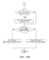
- FIGS. 10A and 10B illustrate a flowchart describing the operation of a design tool according to various examples of the invention.
- FIGS. 11A-11C illustrates an example of the use of an escape outline for component having an array of 1760 pins in a ball grid array.
- FIG. 12 illustrates a flowchart describing the operation of a design tool according to still other examples of the invention.
- FIG. 13 illustrates an example of a pseudo-pin mapping tool that may be employed according to various examples of the invention.
- FIG. 14 illustrates a flowchart describing the operation of a pseudo-pin mapping tool according to various examples of the invention.
- FIG. 15 illustrates the optimization of netlines using a pseudo-pin mapping tool according to various examples of the invention.
- printed circuit board design tools are conventionally implemented using computer-executable software instructions executed by one or more programmable computing devices. Accordingly, one or more aspects of the invention may be embodied by the execution of software instructions on a programmable computing device to perform one or more functions according to the invention. Alternately or additionally, one or more aspects of the invention may be embodied by computer-executable software instructions stored on a computer-readable medium for performing one or more functions according to the invention. Accordingly, the components and operation of a generic programmable computer system through which various embodiments of the invention may be employed will first be described with reference to FIG. 7 .
- FIG. 7 shows an illustrative example of a computing device 701 .
- the computing device 701 includes a computing unit 703 with a processing unit 705 and a system memory 707 .
- the memory 707 may be implemented using any combination of computer readable media that can be accessed by the processing unit 705 .
- the computer readable media may include, for example, microcircuit memory devices such as read-write memory (RAM), read-only memory (ROM), electronically erasable and programmable read-only memory (EEPROM) or flash memory microcircuit devices, CD-ROM disks, digital video disks (DVD), or other optical storage devices.
- the computer readable media may also include magnetic cassettes, magnetic tapes, magnetic disks or other magnetic storage devices, punched media, holographic storage devices, or any other medium that can be used to store desired information.
- the processing unit 705 may be any type of programmable electronic device for executing software instructions, but will conventionally be a microprocessor.
- the processor unit 705 may be a commercially generic programmable microprocessor, such as an Intel® Pentium® or XeonTM microprocessor, an Advanced Micro Devices AthlonTM microprocessor, or Motorola 68K/Coldfire® microprocessor.
- the processing unit 705 may be a custom-manufactured processor, such as a microprocessor designed to optimally perform specific types of mathematical operations.
- FIG. 8 illustrates an example of a multi-core processor unit 505 that may be employed with various embodiments of the invention.
- the processor unit 505 includes a plurality of processor cores 801 .
- Each processor core 801 includes a computing engine 803 and a memory cache 805 .
- a computing engine contains logic devices for performing various computing functions, such as fetching software instructions and then performing the actions specified in the fetched instructions. These actions may include, for example, adding, subtracting, multiplying, and comparing numbers, performing logical operations such as AND, OR, NOR and XOR, and retrieving data.
- Each computing engine 803 may then use its corresponding memory cache 805 to quickly store and retrieve data and/or instructions for execution.
- Each processor core 801 is connected to an interconnect 807 .
- the particular construction of the interconnect 807 may vary depending upon the architecture of the processor unit 801 . With some processor units 801 , such as the Cell microprocessor created by Sony Corporation, Toshiba Corporation and IBM Corporation, the interconnect 807 may be implemented as an interconnect bus. With other processor units 801 , however, such as the OpteronTM and AthlonTM dual-core processors available from Advanced Micro Devices of Sunnyvale, Calif., the interconnect 807 may be implemented as a system request interface device. In any case, the processor cores 801 communicate through the interconnect 807 with an input/output interfaces 809 and a memory controller 811 .
- the input/output interface 809 provides a communication interface between the processor unit 801 and the bus 713 .
- the memory controller 811 controls the exchange of information between the processor unit 801 and the system memory 707 .
- the processor units 801 may include additional components, such as a high-level cache memory accessible shared by the processor cores 801 .
- the processing unit 705 and the system memory 707 are connected, either directly or indirectly, through a bus 713 or alternate communication structure, to one or more peripheral devices.
- the processing unit 705 or the system memory 707 may be directly or indirectly connected to one or more additional memory storage devices, such as a “hard” magnetic disk drive 715 , a removable magnetic disk drive 717 , an optical disk drive 719 , or a flash memory card 721 .
- the processing unit 705 and the system memory 707 also may be directly or indirectly connected to one or more input devices 723 and one or more output devices 725 .
- the input devices 723 may include, for example, a keyboard, a pointing device (such as a mouse, touchpad, stylus, trackball, or joystick), a scanner, a camera, and a microphone.
- the output devices 725 may include, for example, a monitor display, a printer and speakers.
- one or more of the peripheral devices 715 - 125 may be internally housed with the computing unit 703 . Alternately, one or more of the peripheral devices 715 - 125 may be external to the housing for the computing unit 703 and connected to the bus 713 through, for example, a Universal Serial Bus (USB) connection.
- USB Universal Serial Bus
- the computing unit 703 may be directly or indirectly connected to one or more network interfaces 727 for communicating with other devices making up a network.
- the network interface 727 translates data and control signals from the computing unit 703 into network messages according to one or more communication protocols, such as the transmission control protocol (TCP) and the Internet protocol (IP).
- TCP transmission control protocol
- IP Internet protocol
- the interface 727 may employ any suitable connection agent (or combination of agents) for connecting to a network, including, for example, a wireless transceiver, a modem, or an Ethernet connection.
- TCP transmission control protocol
- IP Internet protocol
- connection agent or combination of agents
- the computer 701 is illustrated as an example only, and it not intended to be limiting. Various embodiments of the invention may be implemented using one or more computing devices that include the components of the computer 701 illustrated in FIG. 7 , which include only a subset of the components illustrated in FIG. 7 , or which include an alternate combination of components, including components that are not shown in FIG. 7 . For example, various embodiments of the invention may be implemented using a multi-processor computer, a plurality of single and/or multiprocessor computers arranged into a network, or some combination of both.
- an escape outline is provided in a printed circuit board design.
- the escape outline which typically will enclose a component object, automatically distinguishes escape traces of a breakout from other traces, such as hanger traces.
- a designer may designate a trace as an escape trace for a component simply by routing the trace from a pin of the component to or through the escape outline around that component.
- Some implementations of the invention may even assist a designer in creating escape traces, by “snapping” traces to the escape outline if the traces have an endpoint within a predetermined distance from the escape outline.
- a designer may use an escape outline to automatically route escape traces using an automatic trace routing tool.
- various embodiments of the invention are related to tools for the design of printed circuit boards.
- some implementations of the invention may be used to improve the operation of printed circuit board design tools for creating and modifying breakout routes in a printed circuit board design.
- the terms “design” and “design data” are intended to encompass data describing an entire printed circuit board. This term also is intended to encompass a smaller set of data describing a subset of an entire printed circuit board, however, such as a layer of an printed circuit board, or even a portion of a layer of an printed circuit board.
- the terms “design” and “design data” also are intended to encompass data describing more than one printed circuit board, such as data to be used to create a system of interconnected printed circuit boards.
- designer is intended to encompass a single person creating, modifying, or otherwise editing a printed circuit board design. This term also is intended to encompass a group of persons, collaborating as a team or working as individuals, that creates, modifies, or otherwise edits a printed circuit board design.
- FIG. 9 illustrates a printed circuit board design tool 901 that may incorporate one or more aspects of the invention.
- the design tool 901 includes a user interface module 903 and a design editing module 905 .
- the user interface module 903 may, for example, provide a graphical user interface that allows a designer to add a trace to a printed circuit board design, modify the route of a trace that already exists in a printed circuit board design, specify one or more properties for a trace, or any other conventional trace editing operation for a printed circuit board design.
- the design editing module 905 modifies a printed circuit board design to implement the additions or revisions input through the user interface module 903 .
- the design editing module 905 may perform one or more automatic editing operations. For example, if a user changes the route of a first trace so that it is too close or overlays a second trace, then the design editing module 905 may automatically revise the route to the second trace to maintain some minimum distance between the first trace and the second trace.
- the design tool 901 also includes an escape outline definition module 907 and an escape trace identification module 909 .
- the escape outline definition module 907 receives input from a designer, through the user interface module 903 , specifying the parameters of an escape outline.
- the escape outline definition module 907 creates an escape outline in the printed circuit board design based upon the instructions provided by the designer.
- the escape trace identification module 909 will use the escape outline to determine if a trace is an escape trace or some other type of trace.
- the printed circuit board design being edited by the design tool 901 may be stored in a design storage 911 .
- the design storage 911 typically will be implemented by a magnetic disc, such as the type employed by a magnetic hard disc drive.
- the design storage 911 alternately may be implemented by any desired memory medium, including, for example, a magnetic disc, an optical disc, a flash or other solid state memory device, including a RAM or ROM memory device, or some combination of these devices.
- the design storage 911 is shown as separate from the design tool 901 in FIG. 9 , it should be appreciated that some or all of the design storage 911 may be incorporated into the design tool 901 .
- a component object is a data object in a printed circuit board design representing an electrical component that will be mounted on the printed circuit board.
- the component object may represent any type of component, including active components, such as field programmable gate array device or other powered integrated circuit device.
- the component object alternately may represent a passive component, such as a connector.
- FIG. 1A illustrates an example of a component object 1101 representing a component having an array of 1760 pins in a ball grid array. Accordingly, the component object 1101 includes 1760 pins 1103 , with the location of each pin 1103 corresponding to the location of a physical solder ball pin of the component.
- the designer may input the parameters defining the escape outline through the user interface module 903 .
- the user will specify one or more perimeters for the escape outline, as well as the component object with which the escape outline will be affiliated.
- the designer also may specify one or more properties for the escape outline. As will be discussed in more detail below, these properties may be imparted to traces associated with the escape outline.
- the escape outline definition module 907 adds the escape outline to the printed circuit board design.
- the designer will create an escape outline so that it surrounds its affiliated component object, like the escape outline 1105 shown in FIG. 11B .
- the perimeter of the escape outline 1105 is the same distance from the corresponding side of the component object 1101 .
- the escape outline definition module 907 may allow a designer to specify any desired shape for the perimeter of the escape outline. A user may thus create an escape outline with a perimeter that has some edges closer to its affiliated component object than other edges. Also, in addition to having a rectangularly-shaped perimeter, various implementations of the invention may allow a designer to create an escape outline having a perimeter with other shapes, such as other polygons, circles, ellipses, etc.
- an escape outline may exist in a plurality of layers of a printed circuit board design.
- modern printed circuit boards may have a two or more layers.
- a designer may specify an escape outline having a perimeter in each of one or more different layers of the printed circuit board design. For example, if the printed circuit board design is for a printed circuit board having six layers, the designer may create an escape outline having a perimeter in the design for each of the six layers.
- the escape outline may exist on only specific layers in a printed circuit board design.
- the perimeter of the escape outline may vary from layer to layer of the printed circuit board design.
- the perimeter of the escape outline may be outside of the periphery of its affiliated component object.
- the perimeter of the escape outline may be substantially smaller than the periphery of its affiliated component object. This may be particularly useful, for example, where only a few vias extend from the component object to inner layers of the printed circuit board design. By configuring the perimeter of the escape outline to encompass only those few vias extending from pins of the component object, the designer can preserve space on these inner layers for routing traces unrelated to the component object. It should be noted that various implementations of the invention may allow a user to modify or change features of an escape outline at anytime, include the size and shape of a perimeter of the escape outline, and properties assigned to the escape outline.
- step S 1005 the designer employs the design editing module 905 to edit a trace that extends from a pin of the component object.
- the term “edit” is intended to encompass both creating a new trace and modifying an existing trace.
- the term “extend” is intended to encompass both a direct electrical connection and an indirect electrical connection through one or more intermediary vias or traces.
- a trace extending from a pin as described herein, may extend directly from that pin, or may be connected to the pin through a via which itself is connected to the pin through another trace (or a combination of multiple vias and traces).
- step S 1009 the design editing module 905 provides the trace edit to the escape trace identification module 909 .
- the escape trace identification module 909 determines if the end of the trace is within a threshold distance of the perimeter of the escape outline (more particularly, the perimeter of the escape outline for the layer in which the trace is routed). If the end of the trace is within the threshold distance of the perimeter of escape outline, then the escape trace identification module 909 instructs the design editing module 905 to “snap” the trace to the escape outline. For example, the design editing module 905 may shorten or extend the trace so that the unconnected end of the trace is positioned on the perimeter of the escape outline.
- step S 1015 the escape trace identification module 909 determines if the trace intersects the escape outline. More particularly, the escape trace identification module 909 determines if the trace crosses over the perimeter of the escape outline or if the end of the trace falls on the perimeter of the escape outline. If the trace does intersect the escape outline, then in step S 1017 the escape trace identification module 909 determines that the trace is an escape trace for the component object. With some implementations of the invention, the escape trace identification module 909 may determine that the entire trace is an escape trace. Alternately, with other implementations of the invention, the escape trace identification module 909 may determine that one the portion of the trace falling within the perimeter of the escape outline is an escape trace. If the trace does not intersect the escape outline, then in step S 1019 the escape trace identification module 909 determines that the trace is not an escape trace for the component object.
- each of steps S 1015 through S 1017 may be performed for each trace extending from a pin of the component object as it is edited.
- the escape trace identification module 909 may, for example, update a Boolean flag value for the trace after it has been edited.
- steps S 1015 through S 1017 may be performed concurrently for every trace extending from a pin of the component object.
- the escape trace identification module 909 may postpone performing steps S 1015 through S 1017 until, e.g., a designer makes an edit to the printed circuit board design that would implicate all of the escape traces for the component object, such as a rotation or movement of the component object.
- the design editing module 905 would then perform steps S 1015 through S 1017 for each trace extending from a pin of the component object concurrently, identifying the escape traces for the component object at the same time.
- various embodiments of the invention may omit this feature. That is, various embodiments of the invention may not provide a snap operation, and may instead require a designer to specifically intersect a trace with the escape outline for that trace to be identified as an escape trace by the escape trace identification module 909 .
- escape outlines can assist a designer in manually creating escape traces
- various examples of invention may alternately or additionally facilitate the automatic routing of escape traces using an autorouting operation. For example, rather than manually routing each escape trace to (or through) a point on the escape outline, a designer may instead simply designate a variety of connection points on the escape outline. Based upon these connection points, an autorouting operation can then automatically route traces from pins of the affiliated component object to a corresponding connection point. This aspect of various embodiments of the invention will be discussed with reference to the flowchart shown in FIG. 12 .
- step S 1201 the designer defines an escape outline affiliated with a component object, as discussed in detail above.
- the perimeter of the escape outline may have any desired shape.
- the escape outline may have a perimeter on multiple layers of a printed circuit board design.
- step S 1203 the designer designates one or more connection points along the perimeter (or perimeters) of the escape outline, such that each connection point corresponds to a particular pin of the component object. For example, a designer may create a connection point, C 12 , which corresponds with pin P 12 of the component object. The designer may then create a second connection point, C 637 , which corresponds with pin P 637 of the component object.
- step S 1205 the design editing module 905 employs an autorouting operation to automatically route breakouts from the pins of the component object to their corresponding connection points along the perimeter (or perimeters) of the escape outline.
- the design editing module 905 will automatically route a breakout from the pin P 12 to the connection point C 12 . It also will automatically route another breakout from the pin P 637 to the connection point C 637 .
- the designer can create a connection point for each pin of the object component that will be connected to another component object.
- the design editing module 905 (or any other desired routing tool with automatic breakout routing capability) will automatically create a breakout from each pin to its corresponding connection point.
- the designer can control where the breakout terminates. For example, if the designer wishes to connect the pin P 12 to another device that positioned to the left of the component object, then the designer can locate the connection point C 12 on the left side of the perimeter of the escape outline. Similarly, if the designer wishes to connect the pin P 637 to another device that positioned to the right of the component object, then the designer can locate the connection point C 637 on the right side of the perimeter of the escape outline.
- connection points along the perimeter of an escape outline can be order to effectively reorder the corresponding pins of the component object. This may be particularly useful for, e.g., application specific integrated circuits, since the pin outputs of this circuit cannot ordinarily be changed as with connectors or field programmable gate array circuits.
- various embodiments of the invention may assist an autorouting operation to create breakouts including one or more vias to those different layers.
- the escape outline features provided by various implementations of the invention can assist a designer in creating escape traces for breakouts of a component object.
- a designer can create a breakout for every desired pin of a component object, as illustrated in FIG. 11C .
- a designer can then perform a second routing operation to route traces from the breakouts to other component objects. Because the breakouts extend outside of the dense pin area of the component object, however, this second routing operation typically will be much simpler than attempting to route traces directly to each relevant pin of the component object.
- escape traces of the breakouts extend to or through the escape outline, escape traces of breakouts can be readily distinguished from hanger traces that extend from pins of the component object, but which were not created to extend those pins to any particular net.
- various implementation of the invention may employ an escape outline to associate desired properties with the identified escape traces.
- a designer can specify a minimum width for escape traces identified by the escape outline that is different from other traces (e.g., non-breakout traces).
- a designer may specify a minimum trace clearance for escape traces identified by the escape outline that are different from other, traces.
- escape traces or breakouts containing escape traces identified by the escape outline be moved or otherwise manipulated with their corresponding component object.
- escape traces or breakouts containing escape traces identified by the escape outline
- the escape traces or breakouts containing escape traces
- the escape traces extending from pins of that component object will similarly be rotated and/or inverted, so as to maintain their routing relative to the component object.
- the escape traces or breakouts containing escape traces
- Non-escape traces may be left in their original position and orientation.
- various implementations can ensure that an identified escape trace will continue to be treated as an escape trace unless the designer specifically indicates otherwise.
- some editing tools provide a “Push And Move” or similar feature that automatically edits a trace in response to the designer editing an adjacent trace.
- these editing tools will automatically push the portions of one or more adjacent traces in a similar manner, in order to maintain a minimum separation distance between the traces.
- the editing tool will modify these identified escape traces so that they continue to extend to or through the escape outline (and thus will continue to be identified as escape traces).
- various implementations of the invention may prevent traces from having corners or otherwise being routed along a perimeter of an escape outline.
- various implementations of invention may be used to associate various properties with non-escape traces (e.g., hangers) falling within a perimeter of the escape outline.
- non-escape traces e.g., hangers
- various implementations of the invention may permit a designer to specify minimum width and/or minimum spacing properties for all traces falling within a perimeter of an escape outline, including hangers.
- various implementations of the invention may allow a designer to specify that traces within a perimeter of an escape outline be treated differently than traces that exist outside the perimeter (or perimeters) of the escape outline. For example, if a designer activates an automatic operation that globally removes hangers from the printed circuit board design, the designer may specify that hangers existing with a perimeter of an escape outline be exempted from removal.
- some implementations of the invention may further allow a designer to associate different properties with escape traces or other traces within an escape outline depend upon the layer in which those traces are routed. For example, a designer may assign a first set of properties to escape traces or other traces falling within the perimeter of an escape outline in a first layer of the printed circuit board design. The designer may then assign a second set of properties to escape traces or other traces falling within another perimeter of the escape outline in a second layer of the printed circuit board design.
- an object component may included as part of a library item retrieved from a library.
- the library item also may include a pre-defined escape outline for the component object.
- the library item also may include pre-routed escape traces that extend to or through the escape outline.
- the escape outline can still be used to associate desired properties with escape traces or other traces falling within the escape outline, as discussed above.
- a designer may use a predefined escape outline to control editing of escape traces or other traces within the escape outline, as also discussed above. Still further, some implementations may allow the designer to modify the perimeters or other aspects of a pre-defined escape outline as desired.
- each escape outline typically will identify escape traces for pins of only its affiliated component object.
- Some implementations of the invention may allow a designer to specify different properties for each escape outline, while still other implementations of the invention may alternately or additionally allow a designer to specify one or more global properties for multiple escape outlines.
- While different implementations of the invention can assist a designer in creating and identifying breakouts, various examples of the may alternately or additionally assist a designer in organizing netlines for traces the include or connect to breakouts.
- the use of breakouts may reduce the effectiveness of netline optimization analysis. While a netline optimization analysis can be performed at anytime during the design of a printed circuit board, it typically is performed as part of the task of placing component objects in a printed circuit board design. Moreover, netline optimization analysis is usually completed before general routing of traces in the printed circuit board design is begun. Referring back to FIG. 2 , this figure shows how pins of a component object were reconfigured to prevent the netlines from crossing, to thereby simplify the process for routing traces to the pins.
- breakouts extending from these pins subsequently are created, however, the breakouts may undo or otherwise frustrate the routing advantages provided by reconfiguring the pins based upon a netline optimization analysis.
- This potential disadvantage to employing breakouts is illustrated in FIG. 6 , which show netlines extending from the endpoints of the breakouts rather than the pins. As previously noted, crossing netlines indicate the that corresponding traces would either need to be routed through different layers of the printed circuit board, require a relatively complex routing path, or both.
- Various embodiments of the invention may address this potential disadvantage of using breakouts by treating the ends of breakouts as pseudo-pins. These pseudo-pins are then mapped to a netline optimization analysis rather in place of the actual pins from which the breakouts extend. By performing a pin-swapping operation based upon these pseudo-pins rather than the corresponding pins of the component object, the pin-swapping operation can minimize the likelihood that traces extending from the breakouts will cross.
- FIG. 13 illustrates an example of a pseudo-pin mapping tool 1301 that may be employed according to various examples of the invention.
- the pseudo-pin mapping tool 1301 includes a breakout identification module 1303 and a breakout endpoint determination module 1305 .
- the pseudo-pin mapping tool 1301 may receive a printed circuit board design from, e.g., a design storage 911 .
- the design storage 911 typically will be implemented by a magnetic disc, such as the type employed by a magnetic hard disc drive.
- the design storage 911 alternately may be implemented by any desired memory medium, including, for example, a magnetic disc, an optical disc, a flash or other solid state memory device, including a RAM or ROM memory device, or some combination of these devices.
- the design storage 911 is shown as separate from the pseudo-pin mapping tool 1301 in FIG. 13 , it should be appreciated that some or all of the design storage 911 may be incorporated into the pseudo-pin mapping tool 1301 .
- the pseudo-pin mapping tool 1301 provides pseudo-pin information to a pin-swapping module 1307 .
- the pin-swapping module may employ any desired conventional pin-swapping tool, such as the pin-swapping tool provided in the IO Designer family of printed circuit board design tools available from Mentor Graphics Corporation of Wilsonville, Oreg.
- the pin-swapping module 1307 then performs a netline optimization analysis using the pseudo-pin information, and swaps the corresponding pins in the printed circuit board design accordingly.
- the pin-swapping module 1307 also is shown as separate from the pseudo-pin mapping tool 1301 in FIG. 13 , some or all of the pin-swapping module 1307 may be incorporated into the pseudo-pin mapping tool 1301 .
- the operation of the pseudo-pin mapping tool 1301 will be discussed in more detail with regard to the flowchart illustrated in FIG. 14 .
- the breakout identification module 1303 receives trace information for a component object.
- the breakout identification module 1303 identifies the breakouts for the component objects.
- the breakout identification module 1303 may simply identify any trace extending from a pin of the object component as part of a breakout.
- Still other examples of the invention may identify only those traces extending from a pin of the object component that have a minimum length as part of a breakout.
- Still other implementations of the invention may additionally provide an escape outline for the object component. With these implementations of the invention, the breakout identification module 1303 can easily identify the escape traces of breakouts as discussed in detail above.
- the breakout endpoint determination module 1305 identifies an endpoint for each breakout.
- the breakout endpoint determination module 1305 may simply determine the endpoint of a breakout as the end point of the trace in the breakout extended furthest from the object component.
- the breakout endpoint determination module 1305 may easily identify the endpoint of the breakout as the point at which a trace of the breakout intersects a perimeter of the escape outline.
- the breakout endpoint determination module 1305 provides pseudo-pin information, including the endpoint for each breakout to the pin from which the breakout extends, to the pin-swapping module 1307 . That is, the breakout endpoint determination module 1305 designates the identified endpoint of the breakout as a pseudo-pin, and provides the location of this pseudo-pin to the pin-swapping module 1307 .
- the pseudo-pin is information will also include the name of the actual component object pin represented by the pseudo-pin. With various examples of the invention, the pseudo-pin information also may include other information, such as the name of the net to which the object component pin should be connected, layer information for the pseudo-pin where the breakout may traverse multiple layers, the name of the signal to be conveyed by the breakout, etc.
- the pin-swapping module 1307 will perform a netline optimization analysis using the pseudo-pins provided by the pseudo-pin mapping tool 1301 , rather than the actual pins of the component object.
- conventional pin-swapping routines for netline optimization currently build structures that represent a map of the pins of an object component and their associated netlines. If an actual pin has a corresponding pseudo-pin, however, then the pin-swapping module 1307 will use include the location of the pseudo-pin in its map rather than the actual pin.
- the pseudo-pin mapping tool 1301 can then use the pseudo-pin information to determine which actual pins of the component object should be reordered to optimize the netline arrangement.
- the pin-swapping module 1307 may create a first netline extending from a pseudo-pin P 21 ′ and a second netline extending from a pseudo-pin P 365 ′.
- the pin-swapping module 1307 may determine that the location of pseudo-pin P 21 ′ should be swapped with the location of pseudo-pin P 365 ′.
- the pseudo-pin mapping tool 1301 can then correctly swap the actual pin P 21 with the actual pin P 365 . In this manner, the actual pins of the component object can be reordered so as to reduce the likelihood that their corresponding breakouts will create crossing netlines, as illustrated in FIG. 15 .
Abstract
Description
Claims (8)
Priority Applications (1)
| Application Number | Priority Date | Filing Date | Title |
|---|---|---|---|
| US11/937,411 US8103988B2 (en) | 2006-11-08 | 2007-11-08 | Use of breakouts in printed circuit board designs |
Applications Claiming Priority (3)
| Application Number | Priority Date | Filing Date | Title |
|---|---|---|---|
| US86497006P | 2006-11-08 | 2006-11-08 | |
| US86496906P | 2006-11-08 | 2006-11-08 | |
| US11/937,411 US8103988B2 (en) | 2006-11-08 | 2007-11-08 | Use of breakouts in printed circuit board designs |
Publications (2)
| Publication Number | Publication Date |
|---|---|
| US20080178139A1 US20080178139A1 (en) | 2008-07-24 |
| US8103988B2 true US8103988B2 (en) | 2012-01-24 |
Family
ID=39365386
Family Applications (1)
| Application Number | Title | Priority Date | Filing Date |
|---|---|---|---|
| US11/937,411 Active US8103988B2 (en) | 2006-11-08 | 2007-11-08 | Use of breakouts in printed circuit board designs |
Country Status (2)
| Country | Link |
|---|---|
| US (1) | US8103988B2 (en) |
| WO (1) | WO2008058258A2 (en) |
Cited By (1)
| Publication number | Priority date | Publication date | Assignee | Title |
|---|---|---|---|---|
| US20150198631A1 (en) * | 2014-01-15 | 2015-07-16 | Taiwan Semiconductor Manufacturing Co., Ltd. | Universal Probe Card PCB Design |
Families Citing this family (6)
| Publication number | Priority date | Publication date | Assignee | Title |
|---|---|---|---|---|
| GB2393533A (en) * | 2002-09-27 | 2004-03-31 | Zuken Ltd | Routing of interconnected regions e.g. of electrical circuits |
| JP5223790B2 (en) * | 2009-06-22 | 2013-06-26 | 富士通株式会社 | Printed circuit board design support program, printed circuit board design support method, and printed circuit board design support apparatus |
| TWI433617B (en) * | 2010-11-08 | 2014-04-01 | Delta Electronics Inc | Circuit board |
| WO2014153029A1 (en) * | 2013-03-14 | 2014-09-25 | New York University | System, method and computer-accessible medium for providing secure split manufacturing |
| US10285276B1 (en) * | 2016-09-23 | 2019-05-07 | Cadence Design Systems, Inc. | Method and apparatus to drive layout of arbitrary EM-coil through parametrized cell |
| US10485096B2 (en) | 2017-11-29 | 2019-11-19 | Dell Products L.P. | Differential trace pair system |
Citations (29)
| Publication number | Priority date | Publication date | Assignee | Title |
|---|---|---|---|---|
| US5450290A (en) | 1993-02-01 | 1995-09-12 | International Business Machines Corporation | Printed circuit board with aligned connections and method of making same |
| US5757656A (en) * | 1995-12-20 | 1998-05-26 | Mentor Graphics | Method for routing breakouts |
| US5784262A (en) | 1995-11-06 | 1998-07-21 | Symbios, Inc. | Arrangement of pads and through-holes for semiconductor packages |
| US6150729A (en) | 1999-07-01 | 2000-11-21 | Lsi Logic Corporation | Routing density enhancement for semiconductor BGA packages and printed wiring boards |
| US6198635B1 (en) | 1999-05-18 | 2001-03-06 | Vsli Technology, Inc. | Interconnect layout pattern for integrated circuit packages and the like |
| US6373139B1 (en) | 1999-10-06 | 2002-04-16 | Motorola, Inc. | Layout for a ball grid array |
| US6388890B1 (en) | 2000-06-19 | 2002-05-14 | Nortel Networks Limited | Technique for reducing the number of layers in a multilayer circuit board |
| US20020060318A1 (en) * | 1998-12-03 | 2002-05-23 | Katz Walter M. | Routable high-density interfaces for integrated circuit devices |
| US6406936B1 (en) | 2000-12-13 | 2002-06-18 | Lsi Logic Corporation | Method for increasing trace rows of a ball grid array |
| US20030047348A1 (en) | 2001-09-10 | 2003-03-13 | Rebecca Jessep | Grid array mounting arrangements |
| US20040016117A1 (en) | 2000-06-19 | 2004-01-29 | Aneta Wyrzykowska | Technique for reducing the number of layers in a signal routing device |
| US6720501B1 (en) | 1998-04-14 | 2004-04-13 | Formfactor, Inc. | PC board having clustered blind vias |
| US20040099440A1 (en) | 2000-06-19 | 2004-05-27 | Herman Kwong | Technique for accommodating electronic components on a multiplayer signal routing device |
| US6762366B1 (en) | 2001-04-27 | 2004-07-13 | Lsi Logic Corporation | Ball assignment for ball grid array package |
| US20040136168A1 (en) | 2000-06-19 | 2004-07-15 | Duxbury Guy M.A.F. | Techniques for reducing the number of layers in a multilayer signal routing device |
| US20040212103A1 (en) * | 2000-06-19 | 2004-10-28 | Herman Kwong | Techniques for pin arrangements in circuit chips |
| US20040216916A1 (en) | 2000-06-19 | 2004-11-04 | Aneta Wyrzykowska | Technique for improving power and ground flooding |
| US6833615B2 (en) | 2000-12-29 | 2004-12-21 | Intel Corporation | Via-in-pad with off-center geometry |
| US7017137B2 (en) * | 2001-06-22 | 2006-03-21 | Cadence Design Systems, Inc. | Topological global routing for automated IC package interconnect |
| US20060110848A1 (en) * | 2004-11-19 | 2006-05-25 | Alcatel | Off-width pitch for improved circuit card routing |
| US7061116B2 (en) | 2001-09-26 | 2006-06-13 | Intel Corporation | Arrangement of vias in a substrate to support a ball grid array |
| US7064431B2 (en) | 2002-08-26 | 2006-06-20 | Intel Corporation | Electronic assembly having select spacing of rows and columns of contacts to allow for routing of traces to the contacts |
| US7064279B2 (en) | 2004-09-23 | 2006-06-20 | Motorola, Inc. | Circuit board having an overlapping via |
| US7161812B1 (en) | 2003-04-08 | 2007-01-09 | Nvidia Corporation | System for arraying surface mount grid array contact pads to optimize trace escape routing for a printed circuit board |
| US7343577B2 (en) * | 2005-09-13 | 2008-03-11 | Alcatel | Area array routing masks for improved escape of devices on PCB |
| US7365568B1 (en) * | 2004-09-30 | 2008-04-29 | Xilinx, Inc. | Method and circuit for reducing programmable logic pin counts for large scale logic |
| US20080225502A1 (en) * | 2005-08-10 | 2008-09-18 | Alcatel | Alternating micro-vias and throughboard vias to create PCB routing channels in BGA interconnect grid |
| US7444623B2 (en) * | 2001-08-24 | 2008-10-28 | Formfactor, Inc. | Process and apparatus for adjusting traces |
| US20110011683A1 (en) * | 2009-07-17 | 2011-01-20 | Shimano, Inc. | Hydraulic Caliper Brake For A Bicycle |
-
2007
- 2007-11-08 WO PCT/US2007/084168 patent/WO2008058258A2/en active Application Filing
- 2007-11-08 US US11/937,411 patent/US8103988B2/en active Active
Patent Citations (32)
| Publication number | Priority date | Publication date | Assignee | Title |
|---|---|---|---|---|
| US5450290A (en) | 1993-02-01 | 1995-09-12 | International Business Machines Corporation | Printed circuit board with aligned connections and method of making same |
| US5784262A (en) | 1995-11-06 | 1998-07-21 | Symbios, Inc. | Arrangement of pads and through-holes for semiconductor packages |
| US5757656A (en) * | 1995-12-20 | 1998-05-26 | Mentor Graphics | Method for routing breakouts |
| US6720501B1 (en) | 1998-04-14 | 2004-04-13 | Formfactor, Inc. | PC board having clustered blind vias |
| US20020060318A1 (en) * | 1998-12-03 | 2002-05-23 | Katz Walter M. | Routable high-density interfaces for integrated circuit devices |
| US6198635B1 (en) | 1999-05-18 | 2001-03-06 | Vsli Technology, Inc. | Interconnect layout pattern for integrated circuit packages and the like |
| US6150729A (en) | 1999-07-01 | 2000-11-21 | Lsi Logic Corporation | Routing density enhancement for semiconductor BGA packages and printed wiring boards |
| US6373139B1 (en) | 1999-10-06 | 2002-04-16 | Motorola, Inc. | Layout for a ball grid array |
| US6388890B1 (en) | 2000-06-19 | 2002-05-14 | Nortel Networks Limited | Technique for reducing the number of layers in a multilayer circuit board |
| US20040216916A1 (en) | 2000-06-19 | 2004-11-04 | Aneta Wyrzykowska | Technique for improving power and ground flooding |
| US6545876B1 (en) | 2000-06-19 | 2003-04-08 | Nortel Networks Limited | Technique for reducing the number of layers in a multilayer circuit board |
| US20040016117A1 (en) | 2000-06-19 | 2004-01-29 | Aneta Wyrzykowska | Technique for reducing the number of layers in a signal routing device |
| US20040136168A1 (en) | 2000-06-19 | 2004-07-15 | Duxbury Guy M.A.F. | Techniques for reducing the number of layers in a multilayer signal routing device |
| US20040099440A1 (en) | 2000-06-19 | 2004-05-27 | Herman Kwong | Technique for accommodating electronic components on a multiplayer signal routing device |
| US20040212103A1 (en) * | 2000-06-19 | 2004-10-28 | Herman Kwong | Techniques for pin arrangements in circuit chips |
| US6406936B1 (en) | 2000-12-13 | 2002-06-18 | Lsi Logic Corporation | Method for increasing trace rows of a ball grid array |
| US6833615B2 (en) | 2000-12-29 | 2004-12-21 | Intel Corporation | Via-in-pad with off-center geometry |
| US6762366B1 (en) | 2001-04-27 | 2004-07-13 | Lsi Logic Corporation | Ball assignment for ball grid array package |
| US7051434B2 (en) | 2001-04-27 | 2006-05-30 | Lsi Logic Corporation | Designing a ball assignment for a ball grid array package |
| US7017137B2 (en) * | 2001-06-22 | 2006-03-21 | Cadence Design Systems, Inc. | Topological global routing for automated IC package interconnect |
| US7444623B2 (en) * | 2001-08-24 | 2008-10-28 | Formfactor, Inc. | Process and apparatus for adjusting traces |
| US20030047348A1 (en) | 2001-09-10 | 2003-03-13 | Rebecca Jessep | Grid array mounting arrangements |
| US7061116B2 (en) | 2001-09-26 | 2006-06-13 | Intel Corporation | Arrangement of vias in a substrate to support a ball grid array |
| US7064431B2 (en) | 2002-08-26 | 2006-06-20 | Intel Corporation | Electronic assembly having select spacing of rows and columns of contacts to allow for routing of traces to the contacts |
| US7161812B1 (en) | 2003-04-08 | 2007-01-09 | Nvidia Corporation | System for arraying surface mount grid array contact pads to optimize trace escape routing for a printed circuit board |
| US7064279B2 (en) | 2004-09-23 | 2006-06-20 | Motorola, Inc. | Circuit board having an overlapping via |
| US7365568B1 (en) * | 2004-09-30 | 2008-04-29 | Xilinx, Inc. | Method and circuit for reducing programmable logic pin counts for large scale logic |
| WO2006053891A1 (en) | 2004-11-19 | 2006-05-26 | Alcatel Lucent | Off-width pitch for improved circuit card routing |
| US20060110848A1 (en) * | 2004-11-19 | 2006-05-25 | Alcatel | Off-width pitch for improved circuit card routing |
| US20080225502A1 (en) * | 2005-08-10 | 2008-09-18 | Alcatel | Alternating micro-vias and throughboard vias to create PCB routing channels in BGA interconnect grid |
| US7343577B2 (en) * | 2005-09-13 | 2008-03-11 | Alcatel | Area array routing masks for improved escape of devices on PCB |
| US20110011683A1 (en) * | 2009-07-17 | 2011-01-20 | Shimano, Inc. | Hydraulic Caliper Brake For A Bicycle |
Non-Patent Citations (3)
| Title |
|---|
| Horiuchi et al, "Escape Routing Design to Reduce The Number of Layers in Area Array Packaging", IEEE Transactions on Advanced Packaging, Nov. 1, 2000, vol. 23 No. 4, IEEE, Piscataway, NJ. |
| Ozdal et al., "An Escape Routing Framework for Dense Boards With High-Speed Design Constraints" Computer-Aided Design IICCAD-2005, Nov. 6, 2005, pp. 759-766, ICCAD-2005 IEEE/ACM International Conference, IEEE, Piscataway, NJ. |
| Ozdal et al., "Simultaneous Escape Routing and Layer Assignment for Dense PCBs" Computer Aided Design ICCAD-2004, Nov. 7, 2004, pp. 822-829, ICCAD-2004, IEEE/ACM International Conference, IEEE, Piscataway, NJ. |
Cited By (2)
| Publication number | Priority date | Publication date | Assignee | Title |
|---|---|---|---|---|
| US20150198631A1 (en) * | 2014-01-15 | 2015-07-16 | Taiwan Semiconductor Manufacturing Co., Ltd. | Universal Probe Card PCB Design |
| US9372205B2 (en) * | 2014-01-15 | 2016-06-21 | Taiwan Semiconductor Manufacturing Co., Ltd. | Universal probe card PCB design |
Also Published As
| Publication number | Publication date |
|---|---|
| WO2008058258A8 (en) | 2008-08-14 |
| US20080178139A1 (en) | 2008-07-24 |
| WO2008058258A2 (en) | 2008-05-15 |
| WO2008058258A3 (en) | 2008-09-25 |
Similar Documents
| Publication | Publication Date | Title |
|---|---|---|
| US8103988B2 (en) | Use of breakouts in printed circuit board designs | |
| US6446246B1 (en) | Method and apparatus for detail routing using obstacle carving around terminals | |
| US7519929B2 (en) | Method and computer program product for interlayer connection of arbitrarily complex shapes under asymmetric via enclosure rules | |
| US20080276213A1 (en) | Method of shield line placement for semiconductor integrated circuit, design apparatus for semiconductor integrated circuit, and design program for semiconductor integrated circuit | |
| US9256707B2 (en) | Trace routing according to freeform sketches | |
| JP2006164267A (en) | Method, device, and computer program for reinforcing function of power distribution system in ceramic integrated circuit package | |
| US20080109773A1 (en) | Analyzing Impedance Discontinuities In A Printed Circuit Board | |
| US8356265B2 (en) | Offset fill | |
| US9015647B2 (en) | Dynamic printed circuit board design reuse | |
| CN112235949A (en) | Method, device and equipment for digging differential via hole in printed circuit board design | |
| US7530038B2 (en) | Method and placement tool for designing the layout of an electronic circuit | |
| US8015529B1 (en) | Methods and apparatus for diagonal route shielding | |
| US6496968B1 (en) | Hierarchical wiring method for a semiconductor integrated circuit | |
| EP2214110B1 (en) | Heuristic routing for electronic device layout designs | |
| US20090243121A1 (en) | Semiconductor integrated circuit and layout method for the same | |
| CN106560819A (en) | Control Block Size Reduction Through Ip Migration In Integrated Circuit Device | |
| US20130145340A1 (en) | Determination Of Uniform Colorability Of Layout Data For A Double Patterning Manufacturing Process | |
| JP4668974B2 (en) | Semiconductor device design method, semiconductor device design system, and computer program | |
| JP2005050072A (en) | Cad data converting method, cad data converting system, cad data converting program and method for manufacturing electronic circuit board | |
| US20110072404A1 (en) | Parallel Timing Analysis For Place-And-Route Operations | |
| US20060076547A1 (en) | Three-dimensional viewing and editing of microcircuit design | |
| US8495551B2 (en) | Shaping ports in integrated circuit design | |
| US20200387661A1 (en) | Systems and methods for photolithographic design | |
| US20230068852A1 (en) | Machine learning-based unravel engine for integrated circuit packaging design | |
| US20140201694A1 (en) | Wrap Based Fill In Layout Designs |
Legal Events
| Date | Code | Title | Description |
|---|---|---|---|
| AS | Assignment |
Owner name: MENTOR GRAPHICS CORPORATION, OREGON Free format text: ASSIGNMENT OF ASSIGNORS INTEREST;ASSIGNORS:PFEIL, CHARLES L., MR.;POTTS, HENRY, MR;REEL/FRAME:020760/0213 Effective date: 20080324 |
|
| AS | Assignment |
Owner name: MENTOR GRAPHICS CORPORATION, OREGON Free format text: ASSIGNMENT OF ASSIGNORS INTEREST;ASSIGNORS:PFEIL, CHARLES L.;POTTS, HENRY;REEL/FRAME:021123/0041 Effective date: 20080324 |
|
| STCF | Information on status: patent grant |
Free format text: PATENTED CASE |
|
| FPAY | Fee payment |
Year of fee payment: 4 |
|
| MAFP | Maintenance fee payment |
Free format text: PAYMENT OF MAINTENANCE FEE, 8TH YEAR, LARGE ENTITY (ORIGINAL EVENT CODE: M1552); ENTITY STATUS OF PATENT OWNER: LARGE ENTITY Year of fee payment: 8 |
|
| AS | Assignment |
Owner name: SIEMENS INDUSTRY SOFTWARE INC., TEXAS Free format text: MERGER AND CHANGE OF NAME;ASSIGNORS:MENTOR GRAPHICS CORPORATION;SIEMENS INDUSTRY SOFTWARE INC.;REEL/FRAME:056702/0387 Effective date: 20201230 |
|
| MAFP | Maintenance fee payment |
Free format text: PAYMENT OF MAINTENANCE FEE, 12TH YEAR, LARGE ENTITY (ORIGINAL EVENT CODE: M1553); ENTITY STATUS OF PATENT OWNER: LARGE ENTITY Year of fee payment: 12 |