US8142909B2 - Blue phosphorescent imidazophenanthridine materials - Google Patents
Blue phosphorescent imidazophenanthridine materials Download PDFInfo
- Publication number
- US8142909B2 US8142909B2 US12/044,605 US4460508A US8142909B2 US 8142909 B2 US8142909 B2 US 8142909B2 US 4460508 A US4460508 A US 4460508A US 8142909 B2 US8142909 B2 US 8142909B2
- Authority
- US
- United States
- Prior art keywords
- mmol
- complex
- host
- organic
- mixture
- Prior art date
- Legal status (The legal status is an assumption and is not a legal conclusion. Google has not performed a legal analysis and makes no representation as to the accuracy of the status listed.)
- Active, expires
Links
- 0 *C1=C(*)C2=C3C(=C1*)[Ir](C)([Y])N1=C3N(C(*)=C1*)C1=C2C(*)=C(*)C(*)=C1* Chemical compound *C1=C(*)C2=C3C(=C1*)[Ir](C)([Y])N1=C3N(C(*)=C1*)C1=C2C(*)=C(*)C(*)=C1* 0.000 description 31
- MIWIUZFKVFFPDE-UHFFFAOYSA-N CC1=CC=C2C(=C1)C1=C3C(=CC=C1)[Ir]N1=C3N2C=C1 Chemical compound CC1=CC=C2C(=C1)C1=C3C(=CC=C1)[Ir]N1=C3N2C=C1 MIWIUZFKVFFPDE-UHFFFAOYSA-N 0.000 description 6
- VIWNPTXHCKYQDH-UHFFFAOYSA-N CC.CC(C)(C)C1=C([Rb])C=CC=C1[RaH] Chemical compound CC.CC(C)(C)C1=C([Rb])C=CC=C1[RaH] VIWNPTXHCKYQDH-UHFFFAOYSA-N 0.000 description 4
- WLGRUDDPHKJJAT-UHFFFAOYSA-N CC1=CC=C2C(=C1)C1=C(C=CC=C1)C1=NC=CN21 Chemical compound CC1=CC=C2C(=C1)C1=C(C=CC=C1)C1=NC=CN21 WLGRUDDPHKJJAT-UHFFFAOYSA-N 0.000 description 4
- OYDNTBRGYMZDTM-UHFFFAOYSA-N C.C.CC(C)C1=CC(C(C)C)=C(/C2=C/N3=C4/C5=C(C=CC=C5[Ir]3)C3=CC(CC(C)(C)C)=CC=C3N24)C(C(C)C)=C1.CC(C)C1=CC(C(C)C)=C(C2=CN=C3C4=C(C=CC=C4)C4=CC(CC(C)(C)C)=CC=C4N23)C(C(C)C)=C1 Chemical compound C.C.CC(C)C1=CC(C(C)C)=C(/C2=C/N3=C4/C5=C(C=CC=C5[Ir]3)C3=CC(CC(C)(C)C)=CC=C3N24)C(C(C)C)=C1.CC(C)C1=CC(C(C)C)=C(C2=CN=C3C4=C(C=CC=C4)C4=CC(CC(C)(C)C)=CC=C4N23)C(C(C)C)=C1 OYDNTBRGYMZDTM-UHFFFAOYSA-N 0.000 description 2
- DZQATJPWCNQCHM-UHFFFAOYSA-N C/C1=C/N2C3=CC=CC=C3C3=C4C(=CC=C3)C\N1=C/42 Chemical compound C/C1=C/N2C3=CC=CC=C3C3=C4C(=CC=C3)C\N1=C/42 DZQATJPWCNQCHM-UHFFFAOYSA-N 0.000 description 2
- LJEALDHFHIEESE-UHFFFAOYSA-N C1=CC=C(C2=CC=CC(C3=CC=CC=C3)=C2C2=CN3=C4C5=C(C=CC=C5[Ir]3)C3=CC=CC=C3N24)C=C1 Chemical compound C1=CC=C(C2=CC=CC(C3=CC=CC=C3)=C2C2=CN3=C4C5=C(C=CC=C5[Ir]3)C3=CC=CC=C3N24)C=C1 LJEALDHFHIEESE-UHFFFAOYSA-N 0.000 description 2
- UDECAGDIODUDKR-UHFFFAOYSA-N C1=CC=C2C(=C1)C1=C3C(=CC=C1)[Ir]N1=C3N2C2=C1C=CC=C2 Chemical compound C1=CC=C2C(=C1)C1=C3C(=CC=C1)[Ir]N1=C3N2C2=C1C=CC=C2 UDECAGDIODUDKR-UHFFFAOYSA-N 0.000 description 2
- RNAWNROYAJUHKP-UHFFFAOYSA-N CC(C)(C)CC1=CC=C2N=C(N)C3=C(C=CC=C3)C2=C1.CC(C)C1=CC(C(C)C)=C(C(Br)C=O)C(C(C)C)=C1.CC(C)C1=CC(C(C)C)=C(C2=CN=C3C4=C(C=CC=C4)C4=CC(CC(C)(C)C)=CC=C4N23)C(C(C)C)=C1 Chemical compound CC(C)(C)CC1=CC=C2N=C(N)C3=C(C=CC=C3)C2=C1.CC(C)C1=CC(C(C)C)=C(C(Br)C=O)C(C(C)C)=C1.CC(C)C1=CC(C(C)C)=C(C2=CN=C3C4=C(C=CC=C4)C4=CC(CC(C)(C)C)=CC=C4N23)C(C(C)C)=C1 RNAWNROYAJUHKP-UHFFFAOYSA-N 0.000 description 2
- PTKSKOSCWSEQQV-UHFFFAOYSA-N CC1=C(C)C=C2C(=C1)C1=C3C(=CC=C1)[Ir]N1=C3N2C(C2=C(C3=CC=CC=C3)C=CC=C2C2=CC=CC=C2)=C1 Chemical compound CC1=C(C)C=C2C(=C1)C1=C3C(=CC=C1)[Ir]N1=C3N2C(C2=C(C3=CC=CC=C3)C=CC=C2C2=CC=CC=C2)=C1 PTKSKOSCWSEQQV-UHFFFAOYSA-N 0.000 description 2
- TYDYLORRQPJCHF-UHFFFAOYSA-N CC1=CC=C2C(=C1)C1=C3C(=CC=C1)[Ir]N1=C3N2C(C2=C(C)C=CC=C2C)=C1 Chemical compound CC1=CC=C2C(=C1)C1=C3C(=CC=C1)[Ir]N1=C3N2C(C2=C(C)C=CC=C2C)=C1 TYDYLORRQPJCHF-UHFFFAOYSA-N 0.000 description 2
- VLBNYWPWPIIWEA-UHFFFAOYSA-N CC1=CC=CC(C)=C1/C1=C/N2=C3/C4=C(C=CC=C4C2)C2=CC(CC(C)(C)C)=CC=C2N13 Chemical compound CC1=CC=CC(C)=C1/C1=C/N2=C3/C4=C(C=CC=C4C2)C2=CC(CC(C)(C)C)=CC=C2N13 VLBNYWPWPIIWEA-UHFFFAOYSA-N 0.000 description 2
- GUDHMYXEELTKBZ-UHFFFAOYSA-N CC1=CC=CC(C)=C1C1=CN2=C3C4=C(C=CC=C4[Ir]2)C2=CC(CC(C)(C)C)=CC=C2N13 Chemical compound CC1=CC=CC(C)=C1C1=CN2=C3C4=C(C=CC=C4[Ir]2)C2=CC(CC(C)(C)C)=CC=C2N13 GUDHMYXEELTKBZ-UHFFFAOYSA-N 0.000 description 2
- MPSYEVMLDRGABN-UHFFFAOYSA-N CN(C)C1=CC2=C(C=C1)N1C=CN3=C1C1=C(C=CC=C21)[Ir]3 Chemical compound CN(C)C1=CC2=C(C=C1)N1C=CN3=C1C1=C(C=CC=C21)[Ir]3 MPSYEVMLDRGABN-UHFFFAOYSA-N 0.000 description 2
- OZFBTWVMSXSPAL-UHFFFAOYSA-N COC1=CN2C3=CC=CC=C3C3=C4C(=CC=C3)[Ir]N1=C42 Chemical compound COC1=CN2C3=CC=CC=C3C3=C4C(=CC=C3)[Ir]N1=C42 OZFBTWVMSXSPAL-UHFFFAOYSA-N 0.000 description 2
- YLTONMQNOYJAAH-UHFFFAOYSA-N FC1=CC2=C3C(=C1)[Ir]N1=C3N(C=C1)C1=CC=CC=C12 Chemical compound FC1=CC2=C3C(=C1)[Ir]N1=C3N(C=C1)C1=CC=CC=C12 YLTONMQNOYJAAH-UHFFFAOYSA-N 0.000 description 2
- YUMKXFSCGOCIDT-UHFFFAOYSA-N B=NS.C.C1=CC=C2C(=C1)N=C1N2C2=C(C=CC=C2)C2=NC3=C(C=CC=C3)N21.C1=CC=C2C(=C1)N=C1N3C=CN=C3C3=CC=CC=C3N21.IC1=CC=CC=C1I.N#CC1=C(F)C=CC=C1.N#CC1=CC=CC=C1N1C2=CC=CC=C2N=C1Br.N#CC1=CC=CC=C1N1C=NC2=CC=CC=C21.N/C1=N/C2=NC3=CC=CC=C3N2C2=CC=CC=C21.O=CCCl.[H]N1C=NC2=CC=CC=C21.[NaH] Chemical compound B=NS.C.C1=CC=C2C(=C1)N=C1N2C2=C(C=CC=C2)C2=NC3=C(C=CC=C3)N21.C1=CC=C2C(=C1)N=C1N3C=CN=C3C3=CC=CC=C3N21.IC1=CC=CC=C1I.N#CC1=C(F)C=CC=C1.N#CC1=CC=CC=C1N1C2=CC=CC=C2N=C1Br.N#CC1=CC=CC=C1N1C=NC2=CC=CC=C21.N/C1=N/C2=NC3=CC=CC=C3N2C2=CC=CC=C21.O=CCCl.[H]N1C=NC2=CC=CC=C21.[NaH] YUMKXFSCGOCIDT-UHFFFAOYSA-N 0.000 description 1
- KQSXIMBWMFSXLT-UHFFFAOYSA-N B=NS.C.CC(C)(C)CC1=CC2=C(S1)N1C(Br)=CN=C1C1=C2C=CC=C1.CC(C)(C)CC1=CC2=C(S1)N1C=CN=C1C1=C2C=CC=C1 Chemical compound B=NS.C.CC(C)(C)CC1=CC2=C(S1)N1C(Br)=CN=C1C1=C2C=CC=C1.CC(C)(C)CC1=CC2=C(S1)N1C=CN=C1C1=C2C=CC=C1 KQSXIMBWMFSXLT-UHFFFAOYSA-N 0.000 description 1
- VPSCWLNQTGFFFD-UHFFFAOYSA-N B=NS.CC(C)(C)CC1=C(CC(C)(C)C)C=C(Br)C(N)=C1.CC(C)(C)CC1=C(CC(C)(C)C)C=C(N)C=C1 Chemical compound B=NS.CC(C)(C)CC1=C(CC(C)(C)C)C=C(Br)C(N)=C1.CC(C)(C)CC1=C(CC(C)(C)C)C=C(N)C=C1 VPSCWLNQTGFFFD-UHFFFAOYSA-N 0.000 description 1
- NAUHBNWYTPWBIA-UHFFFAOYSA-N B=NS.CC(C)(C)CC1=CC=C(N)C(Br)=C1.CC(C)(C)CC1=CC=C(N)C=C1 Chemical compound B=NS.CC(C)(C)CC1=CC=C(N)C(Br)=C1.CC(C)(C)CC1=CC=C(N)C=C1 NAUHBNWYTPWBIA-UHFFFAOYSA-N 0.000 description 1
- LGHVHKKUGPUFGO-UHFFFAOYSA-N B=NS.CC(C)CC1=C(CC(C)C)C=C(Br)C(N)=C1.CC(C)CC1=C(CC(C)C)C=C(N)C=C1 Chemical compound B=NS.CC(C)CC1=C(CC(C)C)C=C(Br)C(N)=C1.CC(C)CC1=C(CC(C)C)C=C(N)C=C1 LGHVHKKUGPUFGO-UHFFFAOYSA-N 0.000 description 1
- HJZYSEYAGPNJIO-UHFFFAOYSA-N B=NS.CC1=CC=CC(C)=C1C1=C(Br)N=C2C3=C(C=CC=C3)C3=CC(CC(C)(C)C)=CC=C3N21.CC1=CC=CC(C)=C1C1=CN=C2C3=C(C=CC=C3)C3=CC(CC(C)(C)C)=CC=C3N12 Chemical compound B=NS.CC1=CC=CC(C)=C1C1=C(Br)N=C2C3=C(C=CC=C3)C3=CC(CC(C)(C)C)=CC=C3N21.CC1=CC=CC(C)=C1C1=CN=C2C3=C(C=CC=C3)C3=CC(CC(C)(C)C)=CC=C3N12 HJZYSEYAGPNJIO-UHFFFAOYSA-N 0.000 description 1
- WPTRZPLNVQBWTO-UHFFFAOYSA-N B=NS.CC1=CN(C2=C(C#N)C=CC=C2)C(C)=N1.CC1=NC(C)=C(Br)N1C1=C(C#N)C=CC=C1.CC1=NC(C)=C([N+](=O)[O-])N1C1=C(C#N)C=CC=C1.N#CC1=C(F)C=CC=C1.O=[N+]([O-])O.[H]N1C=C(C)N=C1C.[NaH] Chemical compound B=NS.CC1=CN(C2=C(C#N)C=CC=C2)C(C)=N1.CC1=NC(C)=C(Br)N1C1=C(C#N)C=CC=C1.CC1=NC(C)=C([N+](=O)[O-])N1C1=C(C#N)C=CC=C1.N#CC1=C(F)C=CC=C1.O=[N+]([O-])O.[H]N1C=C(C)N=C1C.[NaH] WPTRZPLNVQBWTO-UHFFFAOYSA-N 0.000 description 1
- BUTAYZBYIGKYBP-UHFFFAOYSA-N B=NS.COC1=CC=C(OC)O1.N#CC1=C(N)C=CC=C1.N#CC1=C(N2C=CC=C2)C=CC=C1.N#CC1=C(N2C=CC=C2Br)C=CC=C1 Chemical compound B=NS.COC1=CC=C(OC)O1.N#CC1=C(N)C=CC=C1.N#CC1=C(N2C=CC=C2)C=CC=C1.N#CC1=C(N2C=CC=C2Br)C=CC=C1 BUTAYZBYIGKYBP-UHFFFAOYSA-N 0.000 description 1
- ZCFCKUVOVYXWML-UHFFFAOYSA-N B=NS.NC1=CC=C(CC2=CC=CC=C2)C=C1.NC1=CC=C(CC2=CC=CC=C2)C=C1Br Chemical compound B=NS.NC1=CC=C(CC2=CC=CC=C2)C=C1.NC1=CC=C(CC2=CC=CC=C2)C=C1Br ZCFCKUVOVYXWML-UHFFFAOYSA-N 0.000 description 1
- XITUXHISZYUABE-UHFFFAOYSA-N BrBr.CC(=O)CC(C)(C)C.CC(C)(C)CC(=O)CBr Chemical compound BrBr.CC(=O)CC(C)(C)C.CC(C)(C)CC(=O)CBr XITUXHISZYUABE-UHFFFAOYSA-N 0.000 description 1
- IMRSCYBUYOSVGG-UHFFFAOYSA-N BrBr.CC(C)(C)CC1=C(CC(C)(C)C)C=C(Br)C=C1.CC(C)(C)CC1=C(CC(C)(C)C)C=CC=C1 Chemical compound BrBr.CC(C)(C)CC1=C(CC(C)(C)C)C=C(Br)C=C1.CC(C)(C)CC1=C(CC(C)(C)C)C=CC=C1 IMRSCYBUYOSVGG-UHFFFAOYSA-N 0.000 description 1
- AZWCKCFAFRWFRY-UHFFFAOYSA-N BrBr.CC(C)(C)CC1=CC=C(Br)C=C1.CC(C)(C)CC1=CC=CC=C1 Chemical compound BrBr.CC(C)(C)CC1=CC=C(Br)C=C1.CC(C)(C)CC1=CC=CC=C1 AZWCKCFAFRWFRY-UHFFFAOYSA-N 0.000 description 1
- FAPCZHMWAQPVRS-UHFFFAOYSA-N BrBr.[H]OC(=O)C1=C(Br)C=C(CC(C)(C)C)S1.[H]OC(=O)C1=CC=C(CC(C)(C)C)S1.[Li]CCCC Chemical compound BrBr.[H]OC(=O)C1=C(Br)C=C(CC(C)(C)C)S1.[H]OC(=O)C1=CC=C(CC(C)(C)C)S1.[Li]CCCC FAPCZHMWAQPVRS-UHFFFAOYSA-N 0.000 description 1
- WZVQDEHBOSPVCZ-UHFFFAOYSA-N BrC1=CC=C2C(=C1)C1=C(C=CC=C1)C1=NC=CN21 Chemical compound BrC1=CC=C2C(=C1)C1=C(C=CC=C1)C1=NC=CN21 WZVQDEHBOSPVCZ-UHFFFAOYSA-N 0.000 description 1
- JJEHXMLQPKZLBQ-UHFFFAOYSA-N BrC1=CC=C2C(=C1)C1=C(C=CC=C1)C1=NC=CN21.BrC1=CN=C2C3=C(C=CC=C3)C3=CC(N4CCCCC4)=CC=C3N12.C1=CC2=C(C=C1)C1=NC=CN1C1=CC=C(N3CCCCC3)C=C12.CC1=CC=CC(C)=C1/C1=C/N2=C3/C4=C(C=CC=C4[Ir]2)C2=CC(N4CCCCC4)=CC=C2N13.CC1=CC=CC(C)=C1C1=CN=C2C3=C(C=CC=C3)C3=CC(N4CCCCC4)=CC=C3N12 Chemical compound BrC1=CC=C2C(=C1)C1=C(C=CC=C1)C1=NC=CN21.BrC1=CN=C2C3=C(C=CC=C3)C3=CC(N4CCCCC4)=CC=C3N12.C1=CC2=C(C=C1)C1=NC=CN1C1=CC=C(N3CCCCC3)C=C12.CC1=CC=CC(C)=C1/C1=C/N2=C3/C4=C(C=CC=C4[Ir]2)C2=CC(N4CCCCC4)=CC=C2N13.CC1=CC=CC(C)=C1C1=CN=C2C3=C(C=CC=C3)C3=CC(N4CCCCC4)=CC=C3N12 JJEHXMLQPKZLBQ-UHFFFAOYSA-N 0.000 description 1
- SLOYVHUZRIEMFJ-UHFFFAOYSA-M BrCCBr.CC(C)(C)CC1=CC2=C(N=CC3=C2C=CC=C3)S1.CC(C)(C)CC1=CC2=C(S1)N(CCBr)=CC1=C2C=CC=C1.[Br-] Chemical compound BrCCBr.CC(C)(C)CC1=CC2=C(N=CC3=C2C=CC=C3)S1.CC(C)(C)CC1=CC2=C(S1)N(CCBr)=CC1=C2C=CC=C1.[Br-] SLOYVHUZRIEMFJ-UHFFFAOYSA-M 0.000 description 1
- OUODLGHMCPABIX-UHFFFAOYSA-N C.C.CC(C)C1=CC(C(C)C)=C(/C2=C/N3=C4/C5=C(C=CC=C5[Ir]3)C3=CC(CC(C)(C)C)=C(CC(C)(C)C)C=C3N24)C(C(C)C)=C1.CC(C)C1=CC(C(C)C)=C(C2=CN=C3C4=C(C=CC=C4)C4=CC(CC(C)(C)C)=C(CC(C)(C)C)C=C4N23)C(C(C)C)=C1 Chemical compound C.C.CC(C)C1=CC(C(C)C)=C(/C2=C/N3=C4/C5=C(C=CC=C5[Ir]3)C3=CC(CC(C)(C)C)=C(CC(C)(C)C)C=C3N24)C(C(C)C)=C1.CC(C)C1=CC(C(C)C)=C(C2=CN=C3C4=C(C=CC=C4)C4=CC(CC(C)(C)C)=C(CC(C)(C)C)C=C4N23)C(C(C)C)=C1 OUODLGHMCPABIX-UHFFFAOYSA-N 0.000 description 1
- IJBGTKPJFKYXPO-UHFFFAOYSA-N C.C.CC1=CC=CC(C)=C1/C1=C/N2=C3/C4=C(C=CC=C4[Ir]2)C2=CC(CC(C)(C)C)=C(CC(C)(C)C)C=C2N13.CC1=CC=CC(C)=C1C1=CN=C2C3=C(C=CC=C3)C3=CC(CC(C)(C)C)=C(CC(C)(C)C)C=C3N12 Chemical compound C.C.CC1=CC=CC(C)=C1/C1=C/N2=C3/C4=C(C=CC=C4[Ir]2)C2=CC(CC(C)(C)C)=C(CC(C)(C)C)C=C2N13.CC1=CC=CC(C)=C1C1=CN=C2C3=C(C=CC=C3)C3=CC(CC(C)(C)C)=C(CC(C)(C)C)C=C3N12 IJBGTKPJFKYXPO-UHFFFAOYSA-N 0.000 description 1
- NSAYWEIJIHLXOU-UHFFFAOYSA-N C.C.CC1=CC=CC(C)=C1/C1=C/N2=C3/C4=C(C=CC=C4[Ir]2)C2=CC(CC(C)(C)C)=CC=C2N13.CC1=CC=CC(C)=C1C1=CN=C2C3=C(C=CC=C3)C3=CC(CC(C)(C)C)=CC=C3N12 Chemical compound C.C.CC1=CC=CC(C)=C1/C1=C/N2=C3/C4=C(C=CC=C4[Ir]2)C2=CC(CC(C)(C)C)=CC=C2N13.CC1=CC=CC(C)=C1C1=CN=C2C3=C(C=CC=C3)C3=CC(CC(C)(C)C)=CC=C3N12 NSAYWEIJIHLXOU-UHFFFAOYSA-N 0.000 description 1
- OXBXAHNWNXLHPQ-UHFFFAOYSA-N C.C.[H]N1C=CN=C1.[H]N1C=NC(C)=C1.[H]N1C=NC(C)=C1C Chemical compound C.C.[H]N1C=CN=C1.[H]N1C=NC(C)=C1.[H]N1C=NC(C)=C1C OXBXAHNWNXLHPQ-UHFFFAOYSA-N 0.000 description 1
- JUXVUTHBPXEPTA-FLCFRILYSA-M C.C1=CC=C(C2=CC3=C(C=C2C2=CC=CC=C2)C2=C(C=C(C4=CC=CC=C4)C(C4=CC=CC=C4)=C2)C2=C3C=C(C3=CC=CC=C3)C(C3=CC=CC=C3)=C2)C=C1.C=C1O[Ir]2(C3=CC(F)=CC(F)=C3C3=N2C=CC=C3)N2=C1C=CC=C2.CC1=CC=CN2=C1C1=CC=CC=C1C2.[3H]P Chemical compound C.C1=CC=C(C2=CC3=C(C=C2C2=CC=CC=C2)C2=C(C=C(C4=CC=CC=C4)C(C4=CC=CC=C4)=C2)C2=C3C=C(C3=CC=CC=C3)C(C3=CC=CC=C3)=C2)C=C1.C=C1O[Ir]2(C3=CC(F)=CC(F)=C3C3=N2C=CC=C3)N2=C1C=CC=C2.CC1=CC=CN2=C1C1=CC=CC=C1C2.[3H]P JUXVUTHBPXEPTA-FLCFRILYSA-M 0.000 description 1
- PLABXMKFNPJEJZ-UHFFFAOYSA-N C.CC(C)(C)CC1=CC=C(Br)C=C1.CC(C)(C)CC1=CC=C(N)C=C1 Chemical compound C.CC(C)(C)CC1=CC=C(Br)C=C1.CC(C)(C)CC1=CC=C(N)C=C1 PLABXMKFNPJEJZ-UHFFFAOYSA-N 0.000 description 1
- LFFMYLSURSEYSF-UHFFFAOYSA-N C.CC(C)(C)CC1=CC=C(N)C(Br)=C1.CC(C)(C)CC1=CC=C(NC2=NC3=CC=C(CC(C)(C)C)C=C3C3=C2C=CC=C3)C(Br)=C1.CC(C)(C)CC1=CC=C2N=C(Cl)C3=C(C=CC=C3)C2=C1 Chemical compound C.CC(C)(C)CC1=CC=C(N)C(Br)=C1.CC(C)(C)CC1=CC=C(NC2=NC3=CC=C(CC(C)(C)C)C=C3C3=C2C=CC=C3)C(Br)=C1.CC(C)(C)CC1=CC=C2N=C(Cl)C3=C(C=CC=C3)C2=C1 LFFMYLSURSEYSF-UHFFFAOYSA-N 0.000 description 1
- DVAVBBAWXZDGKM-UHFFFAOYSA-N C.CC(C)C1=CC(C(C)C)=C(/C2=C/N3=C4/C5=C(C=CC=C5[Ir]3)C3=CC(CC(C)(C)C)=CC=C3N24)C(C(C)C)=C1.CC1=CC=C2C(=C1)C1=C3C(=CC=C1)CN1=C\3N2/C(C2=C(C(C)C)C=CC=C2C(C)C)=C\1 Chemical compound C.CC(C)C1=CC(C(C)C)=C(/C2=C/N3=C4/C5=C(C=CC=C5[Ir]3)C3=CC(CC(C)(C)C)=CC=C3N24)C(C(C)C)=C1.CC1=CC=C2C(=C1)C1=C3C(=CC=C1)CN1=C\3N2/C(C2=C(C(C)C)C=CC=C2C(C)C)=C\1 DVAVBBAWXZDGKM-UHFFFAOYSA-N 0.000 description 1
- NEQNBBAAJIAYIP-UHFFFAOYSA-N C.CC(C)CC1=C(CC(C)C)C=C2C(=C1)N=C(N)C1=C2C=CC=C1.CC1=CC=CC(C)=C1C(Br)C=O.CC1=CC=CC(C)=C1C1=CN=C2C3=C(C=CC=C3)C3=CC(CC(C)C)=C(CC(C)C)C=C3N12 Chemical compound C.CC(C)CC1=C(CC(C)C)C=C2C(=C1)N=C(N)C1=C2C=CC=C1.CC1=CC=CC(C)=C1C(Br)C=O.CC1=CC=CC(C)=C1C1=CN=C2C3=C(C=CC=C3)C3=CC(CC(C)C)=C(CC(C)C)C=C3N12 NEQNBBAAJIAYIP-UHFFFAOYSA-N 0.000 description 1
- RTIUKTDUFSARFJ-UHFFFAOYSA-N C.CC1=CC=CC(C)=C1/C1=C/N2=C3/C4=C(C=CC=C4[Ir]2)C2=C(SC(CC(C)(C)C)=C2)N13.CC1=CC=CC(C)=C1C1=CN=C2C3=C(C=CC=C3)C3=C(SC(CC(C)(C)C)=C3)N12 Chemical compound C.CC1=CC=CC(C)=C1/C1=C/N2=C3/C4=C(C=CC=C4[Ir]2)C2=C(SC(CC(C)(C)C)=C2)N13.CC1=CC=CC(C)=C1C1=CN=C2C3=C(C=CC=C3)C3=C(SC(CC(C)(C)C)=C3)N12 RTIUKTDUFSARFJ-UHFFFAOYSA-N 0.000 description 1
- UODRAPVQVUCEPS-UHFFFAOYSA-N C.CC1=CC=CC(C)=C1C(Br)C=O.CC1=CC=CC(C)=C1C1=CN=C2C3=C(C=CC=C3)C3=CC(CC4=CC=CC=C4)=CC=C3N12.NC1=NC2=CC=C(CC3=CC=CC=C3)C=C2C2=C1C=CC=C2 Chemical compound C.CC1=CC=CC(C)=C1C(Br)C=O.CC1=CC=CC(C)=C1C1=CN=C2C3=C(C=CC=C3)C3=CC(CC4=CC=CC=C4)=CC=C3N12.NC1=NC2=CC=C(CC3=CC=CC=C3)C=C2C2=C1C=CC=C2 UODRAPVQVUCEPS-UHFFFAOYSA-N 0.000 description 1
- FBPBNPXIQDIQQN-UHFFFAOYSA-N C.CC1=CC=CC(C)=C1C1=CN2=C3C4=C(/C=C\C=C/4[Ir]2)C2=C(N=C(C)N2CC(C)(C)C)N13.CC1=CC=CC(C)=C1C1=CN=C2C3=C(C=CC=C3)C3=C(N=C(C)N3CC(C)(C)C)N12 Chemical compound C.CC1=CC=CC(C)=C1C1=CN2=C3C4=C(/C=C\C=C/4[Ir]2)C2=C(N=C(C)N2CC(C)(C)C)N13.CC1=CC=CC(C)=C1C1=CN=C2C3=C(C=CC=C3)C3=C(N=C(C)N3CC(C)(C)C)N12 FBPBNPXIQDIQQN-UHFFFAOYSA-N 0.000 description 1
- WCAJPVSMGOHRRV-UHFFFAOYSA-N C.CC1=CC=CC(C)=C1C1=CN2=C3C4=C(/C=C\C=C/4[Ir]2)C2=C(N=C(CC(C)(C)C)N2CC(C)(C)C)N13.CC1=CC=CC(C)=C1C1=CN=C2C3=C(C=CC=C3)C3=C(N=C(CC(C)(C)C)N3CC(C)(C)C)N12 Chemical compound C.CC1=CC=CC(C)=C1C1=CN2=C3C4=C(/C=C\C=C/4[Ir]2)C2=C(N=C(CC(C)(C)C)N2CC(C)(C)C)N13.CC1=CC=CC(C)=C1C1=CN=C2C3=C(C=CC=C3)C3=C(N=C(CC(C)(C)C)N3CC(C)(C)C)N12 WCAJPVSMGOHRRV-UHFFFAOYSA-N 0.000 description 1
- SKINZTJQXXPSJN-UHFFFAOYSA-N C/C1=C(C)/N2=C3/C4=C(C=CC=C4[Ir]2)C2=CC=CC=C2N13.C/C1=C/N2C3=C(C=C(CC(C)(C)C)C=C3)C3=C4C(=CC=C3)[Ir]\N1=C/42.C/C1=C/N2C3=CC=CC=C3C3=C4C(=CC=C3)[Ir]\N1=C/42.CC(C)(C)CC1=CC2=C(C=C1)N1C3=C(C=CC(CC(C)(C)C)=C3)/N3=C\1C1=C2C=CC=C1[Ir]3.CC(C)C1=CC(C(C)C)=C(/C2=C/N3=C4/C5=C(C=CC=C5[Ir]3)C3=C(C=CC(CC(C)(C)C)=C3)N24)C(C(C)C)=C1 Chemical compound C/C1=C(C)/N2=C3/C4=C(C=CC=C4[Ir]2)C2=CC=CC=C2N13.C/C1=C/N2C3=C(C=C(CC(C)(C)C)C=C3)C3=C4C(=CC=C3)[Ir]\N1=C/42.C/C1=C/N2C3=CC=CC=C3C3=C4C(=CC=C3)[Ir]\N1=C/42.CC(C)(C)CC1=CC2=C(C=C1)N1C3=C(C=CC(CC(C)(C)C)=C3)/N3=C\1C1=C2C=CC=C1[Ir]3.CC(C)C1=CC(C(C)C)=C(/C2=C/N3=C4/C5=C(C=CC=C5[Ir]3)C3=C(C=CC(CC(C)(C)C)=C3)N24)C(C(C)C)=C1 SKINZTJQXXPSJN-UHFFFAOYSA-N 0.000 description 1
- VRJGIWHGDQRWAR-UHFFFAOYSA-N C/C1=C(C)/N2=C3/C4=C(C=CC=C4[Ir]2)C2=CC=CC=C2N13.CC1=C(C)N2C3=CC=CC=C3C3=C(C=CC=C3)C2=N1 Chemical compound C/C1=C(C)/N2=C3/C4=C(C=CC=C4[Ir]2)C2=CC=CC=C2N13.CC1=C(C)N2C3=CC=CC=C3C3=C(C=CC=C3)C2=N1 VRJGIWHGDQRWAR-UHFFFAOYSA-N 0.000 description 1
- JGLUYCODTBNOQJ-UHFFFAOYSA-N C/C1=C/N2C3=CC=C(CC(C)(C)C)C=C3C3=C4C(=CC=C3)[Ir]\N1=C/42.CC1=CN2C3=CC=C(CC(C)(C)C)C=C3C3=C(C=CC=C3)C2=N1 Chemical compound C/C1=C/N2C3=CC=C(CC(C)(C)C)C=C3C3=C4C(=CC=C3)[Ir]\N1=C/42.CC1=CN2C3=CC=C(CC(C)(C)C)C=C3C3=C(C=CC=C3)C2=N1 JGLUYCODTBNOQJ-UHFFFAOYSA-N 0.000 description 1
- LNDNBULYDOSJCY-UHFFFAOYSA-N C/C1=C/N2C3=CC=CC=C3C3=C4C(=CC=C3)[Ir]\N1=C/42.C1=CC=C2C(=C1)C1=C3C(=CC=C1)[Ir]N1=C\3N2/C=C\1.CCCC.CCCC.CCCC Chemical compound C/C1=C/N2C3=CC=CC=C3C3=C4C(=CC=C3)[Ir]\N1=C/42.C1=CC=C2C(=C1)C1=C3C(=CC=C1)[Ir]N1=C\3N2/C=C\1.CCCC.CCCC.CCCC LNDNBULYDOSJCY-UHFFFAOYSA-N 0.000 description 1
- HUTAYTVCIFTOMW-UHFFFAOYSA-N C/C1=C/N2C3=CC=CC=C3C3=C4C(=CC=C3)[Ir]\N1=C/42.CC1=CN2C3=CC=CC=C3C3=C(C=CC=C3)C2=N1 Chemical compound C/C1=C/N2C3=CC=CC=C3C3=C4C(=CC=C3)[Ir]\N1=C/42.CC1=CN2C3=CC=CC=C3C3=C(C=CC=C3)C2=N1 HUTAYTVCIFTOMW-UHFFFAOYSA-N 0.000 description 1
- SEACOMXULQNYSY-UHFFFAOYSA-N C1=C2C(=CC=C1C1CCCCC1)N1/C=C\N3=C1C1=C2/C=C\C=C/1[Ir]3 Chemical compound C1=C2C(=CC=C1C1CCCCC1)N1/C=C\N3=C1C1=C2/C=C\C=C/1[Ir]3 SEACOMXULQNYSY-UHFFFAOYSA-N 0.000 description 1
- NAIQEKFLJNQWIG-UHFFFAOYSA-N C1=CC2=C(C=C1)C1=C(S2)N2C=CN3=C2C2=C(C=CC=C21)[Ir]3 Chemical compound C1=CC2=C(C=C1)C1=C(S2)N2C=CN3=C2C2=C(C=CC=C21)[Ir]3 NAIQEKFLJNQWIG-UHFFFAOYSA-N 0.000 description 1
- LHSVKGMDTIEPGH-UHFFFAOYSA-N C1=CC2=C(C=C1)C1=C3C(=CC=C1)C1=C4C(=CC=C1)[Ir]N1=C4N3C2=C1 Chemical compound C1=CC2=C(C=C1)C1=C3C(=CC=C1)C1=C4C(=CC=C1)[Ir]N1=C4N3C2=C1 LHSVKGMDTIEPGH-UHFFFAOYSA-N 0.000 description 1
- CEQAVKPAHRHFMO-UHFFFAOYSA-N C1=CC2=C(C=C1)N1C3=CC=CC4=C3C3=N(C=CN3C1=N2)[Ir]4 Chemical compound C1=CC2=C(C=C1)N1C3=CC=CC4=C3C3=N(C=CN3C1=N2)[Ir]4 CEQAVKPAHRHFMO-UHFFFAOYSA-N 0.000 description 1
- DNLRHQVNTQLFFW-UHFFFAOYSA-N C1=CC2=C(C=C1)N1C3=CC=CC4=C3C3=N([Ir]4)C4=C(C=CC=C4)N3C1=N2 Chemical compound C1=CC2=C(C=C1)N1C3=CC=CC4=C3C3=N([Ir]4)C4=C(C=CC=C4)N3C1=N2 DNLRHQVNTQLFFW-UHFFFAOYSA-N 0.000 description 1
- XFMKDMPGDPSWTG-UHFFFAOYSA-N C1=CC2=C(C=C1)N1C3=CC=CC4=C3C3=N([Ir]4)C4=C(C=CC=C4)N3C1=N2.C1=CC=C2C(=C1)C1=NC3=C(C=CC=C3)N1C1=NC3=C(C=CC=C3)N21 Chemical compound C1=CC2=C(C=C1)N1C3=CC=CC4=C3C3=N([Ir]4)C4=C(C=CC=C4)N3C1=N2.C1=CC=C2C(=C1)C1=NC3=C(C=CC=C3)N1C1=NC3=C(C=CC=C3)N21 XFMKDMPGDPSWTG-UHFFFAOYSA-N 0.000 description 1
- DBVRTRZRXXYXMS-UHFFFAOYSA-N C1=CC2=C3C(=C1)C1=C(SC=C1)N1C=CN(=C31)[Ir]2 Chemical compound C1=CC2=C3C(=C1)C1=C(SC=C1)N1C=CN(=C31)[Ir]2 DBVRTRZRXXYXMS-UHFFFAOYSA-N 0.000 description 1
- CYXFCDKMRMKAPC-UHFFFAOYSA-N C1=CC2=C3C(=C1)N1C(=NC4=C1C=CN=C4)N1C4=C(C=CN=C4)N(=C31)[Ir]2 Chemical compound C1=CC2=C3C(=C1)N1C(=NC4=C1C=CN=C4)N1C4=C(C=CN=C4)N(=C31)[Ir]2 CYXFCDKMRMKAPC-UHFFFAOYSA-N 0.000 description 1
- JXBLFGZGLUBIOS-UHFFFAOYSA-N C1=CC2=C3C(=C1)N1C=CC=C1C1=C3N(=CO1)[Ir]2 Chemical compound C1=CC2=C3C(=C1)N1C=CC=C1C1=C3N(=CO1)[Ir]2 JXBLFGZGLUBIOS-UHFFFAOYSA-N 0.000 description 1
- XEZLEZLUMHUQMN-UHFFFAOYSA-N C1=CC2=C3C(=C1)N1C=CC=C1N1C=CN(=C31)[Ir]2 Chemical compound C1=CC2=C3C(=C1)N1C=CC=C1N1C=CN(=C31)[Ir]2 XEZLEZLUMHUQMN-UHFFFAOYSA-N 0.000 description 1
- HYHDIHOMSQXLNR-UHFFFAOYSA-N C1=CC2=C3C(=C1)N1C=CN=C1N1C4=C(C=CN=C4)N(=C31)[Ir]2 Chemical compound C1=CC2=C3C(=C1)N1C=CN=C1N1C4=C(C=CN=C4)N(=C31)[Ir]2 HYHDIHOMSQXLNR-UHFFFAOYSA-N 0.000 description 1
- QBZOWAZZDGNLPN-UHFFFAOYSA-N C1=CC2=C3C(=C1)N1C=CN=C1N1C4=C(N=CS4)N([Ir]2)C31 Chemical compound C1=CC2=C3C(=C1)N1C=CN=C1N1C4=C(N=CS4)N([Ir]2)C31 QBZOWAZZDGNLPN-UHFFFAOYSA-N 0.000 description 1
- BUDBZTSTABAVMV-UHFFFAOYSA-N C1=CC2=C3C(=C1)N1C=CN=C1N1C=CN(=C31)[Ir]2 Chemical compound C1=CC2=C3C(=C1)N1C=CN=C1N1C=CN(=C31)[Ir]2 BUDBZTSTABAVMV-UHFFFAOYSA-N 0.000 description 1
- OYFAXXRWBKXJLQ-UHFFFAOYSA-N C1=CC2=C3C(=C1)N1C=NC=C1C1=C3N(=CO1)[Ir]2 Chemical compound C1=CC2=C3C(=C1)N1C=NC=C1C1=C3N(=CO1)[Ir]2 OYFAXXRWBKXJLQ-UHFFFAOYSA-N 0.000 description 1
- FQIZGJCUMAZXKP-UHFFFAOYSA-N C1=CC2=C3C(=C1)N1C=NC=C1N1C=CN(=C31)[Ir]2 Chemical compound C1=CC2=C3C(=C1)N1C=NC=C1N1C=CN(=C31)[Ir]2 FQIZGJCUMAZXKP-UHFFFAOYSA-N 0.000 description 1
- FDZZNUUXZVKGLO-UHFFFAOYSA-N C1=CC2=C3C(=C1)N1N=CC=C1N1C4=C(C=CC=C4)N(=C31)[Ir]2 Chemical compound C1=CC2=C3C(=C1)N1N=CC=C1N1C4=C(C=CC=C4)N(=C31)[Ir]2 FDZZNUUXZVKGLO-UHFFFAOYSA-N 0.000 description 1
- DOUXSBQECCLIDR-UHFFFAOYSA-N C1=CC2=C3C(=C1)N1N=CC=C1N1C=CN(=C31)[Ir]2 Chemical compound C1=CC2=C3C(=C1)N1N=CC=C1N1C=CN(=C31)[Ir]2 DOUXSBQECCLIDR-UHFFFAOYSA-N 0.000 description 1
- CFQZBVANOORJEF-UHFFFAOYSA-N C1=CC2=C3C(=C1)[Ir]N1=C3N(C=C1)C1=C(C3=CC=NC=C3)C=CC=C21 Chemical compound C1=CC2=C3C(=C1)[Ir]N1=C3N(C=C1)C1=C(C3=CC=NC=C3)C=CC=C21 CFQZBVANOORJEF-UHFFFAOYSA-N 0.000 description 1
- OCCONMIOXIUFMQ-UHFFFAOYSA-N C1=CC2=C3C(=C1)[Ir]N1=C3N(C=C1)C1=C(C3=CN=CN=C3)C=CC=C21 Chemical compound C1=CC2=C3C(=C1)[Ir]N1=C3N(C=C1)C1=C(C3=CN=CN=C3)C=CC=C21 OCCONMIOXIUFMQ-UHFFFAOYSA-N 0.000 description 1
- UGVJUWWGVBRALJ-UHFFFAOYSA-N C1=CC2=C3C(=C1)[Ir]N1=C3N(C=C1)C1=CC3=C(C=C12)CCC3 Chemical compound C1=CC2=C3C(=C1)[Ir]N1=C3N(C=C1)C1=CC3=C(C=C12)CCC3 UGVJUWWGVBRALJ-UHFFFAOYSA-N 0.000 description 1
- LWMSEMHZPHFBIZ-UHFFFAOYSA-N C1=CC2=C3C(=C1)[Ir]N1=C3N(C=C1)C1=CC3=C4C(=C12)CCCN4CCC3 Chemical compound C1=CC2=C3C(=C1)[Ir]N1=C3N(C=C1)C1=CC3=C4C(=C12)CCCN4CCC3 LWMSEMHZPHFBIZ-UHFFFAOYSA-N 0.000 description 1
- MVQWULHZPUNAEJ-UHFFFAOYSA-N C1=CC2=C3C(=C1)[Ir]N1=C3N(C=C1)C1=CC=NC=C12 Chemical compound C1=CC2=C3C(=C1)[Ir]N1=C3N(C=C1)C1=CC=NC=C12 MVQWULHZPUNAEJ-UHFFFAOYSA-N 0.000 description 1
- OYTXDKYLYOJPPR-UHFFFAOYSA-N C1=CC2=C3C(=C1)[Ir]N1=C3N(C=C1)C1=CN=CC=C12 Chemical compound C1=CC2=C3C(=C1)[Ir]N1=C3N(C=C1)C1=CN=CC=C12 OYTXDKYLYOJPPR-UHFFFAOYSA-N 0.000 description 1
- XGFGLCKZJNTCPW-UHFFFAOYSA-N C1=CC2=C3C(=C1)[Ir]N1=C3N(C=N1)C1=CN=CC=C12 Chemical compound C1=CC2=C3C(=C1)[Ir]N1=C3N(C=N1)C1=CN=CC=C12 XGFGLCKZJNTCPW-UHFFFAOYSA-N 0.000 description 1
- CKWFUFIYHFLPRC-UHFFFAOYSA-N C1=CC2=C3C(=C1)[Ir]N1=C\3N(\C=C/1)C1=CC=C(C3CCCCC3)C=C12.CC1=C(C)C=C2C(=C1)C1=C3C(=CC=C1)[Ir]N1=C\3N2/C=C\1.CC1=CC(C)=C2C(=C1)C1=C3C(=CC=C1)[Ir]N1=C\3N2/C=C\1.CC1=CC=C(C2=C3C(=CC(C)=C2)C2=C4C(=CC=C2)[Ir]N2=C\4N3/C=C\2)C=C1.CC1=CC=C2C(=C1)C1=C3C(=CC=C1)[Ir]N1=C\3N2/C=C\1.CC1=CC=CC(C)=C1C1=CC=C2C(=C1)C1=C3C(=CC=C1)[Ir]N1=C\3N2/C=C\1 Chemical compound C1=CC2=C3C(=C1)[Ir]N1=C\3N(\C=C/1)C1=CC=C(C3CCCCC3)C=C12.CC1=C(C)C=C2C(=C1)C1=C3C(=CC=C1)[Ir]N1=C\3N2/C=C\1.CC1=CC(C)=C2C(=C1)C1=C3C(=CC=C1)[Ir]N1=C\3N2/C=C\1.CC1=CC=C(C2=C3C(=CC(C)=C2)C2=C4C(=CC=C2)[Ir]N2=C\4N3/C=C\2)C=C1.CC1=CC=C2C(=C1)C1=C3C(=CC=C1)[Ir]N1=C\3N2/C=C\1.CC1=CC=CC(C)=C1C1=CC=C2C(=C1)C1=C3C(=CC=C1)[Ir]N1=C\3N2/C=C\1 CKWFUFIYHFLPRC-UHFFFAOYSA-N 0.000 description 1
- YSJNPJXLPFQUDT-UHFFFAOYSA-N C1=CC2=C3C(=C1)[Pt]14C5=C6C(=CC=C5)N5C=CN=C5N5C=C(CCC7=CN(C8=NC=CN82)C3=N71)N4=C65 Chemical compound C1=CC2=C3C(=C1)[Pt]14C5=C6C(=CC=C5)N5C=CN=C5N5C=C(CCC7=CN(C8=NC=CN82)C3=N71)N4=C65 YSJNPJXLPFQUDT-UHFFFAOYSA-N 0.000 description 1
- DIOGAVGHKWNVES-PIEMELFGSA-N C1=CC=C(C/C2=C/N3C4=C(C=CC=C4)C4=C5C(=CC=C4)C\N2=C/53)C=C1.CC.CC(C)(C)CC1=CC2=C(C=C1)N1C=C3CCc4c-c5cC(=C4)CC/C4=C/N6C7=C(C=C(CC(C)(C)C)C=C7)C7=C8C(=CC=C7)[Ir]79(C%10=CC=CC%11=C%10/C%10=N7/C(=C\N%10C7=C%11C=C(CC(C)(C)C)C=C7)CC5)(/C5=C/C=C\C2=C5C1=N39)\N4=C/86.CC(C)/C1=C/N2C3=C(C=CC=C3)C3=C4C(=CC=C3)C\N1=C/42.CC/C1=C/N2C3=C(C=CC=C3)C3=C4C(=CC=C3)C\N1=C/42.CC1=CC2=C(C=C1)N1/C=C(CC(C)(C)C)\N3=C/1C1=C2C=CC=C1C3.CCC/C1=C/N2C3=C(C=C(CC(C)(C)C)C=C3)C3=C4C(=CC=C3)[Ir]356(C7=CC=CC8=C7/C7=N3/C(=C\N7C3=C8C=C(CC(C)(C)C)C=C3)CC3=C[C@H](CCC3)CC3=CN7C8=C(C=C(CC(C)(C)C)C=C8)C8=C(C7=N35)/C6=C\C=C/8)\N1=C/42.CN(C)/C1=C/N2C3=C(C=CC=C3)C3=C4C(=CC=C3)C\N1=C/42.CO/C1=C/N2C3=C(C=CC=C3)C3=C4C(=CC=C3)C\N1=C/42.C[Si](C)(C)/C1=C/N2C3=C(C=CC=C3)C3=C4C(=CC=C3)C\N1=C/42 Chemical compound C1=CC=C(C/C2=C/N3C4=C(C=CC=C4)C4=C5C(=CC=C4)C\N2=C/53)C=C1.CC.CC(C)(C)CC1=CC2=C(C=C1)N1C=C3CCc4c-c5cC(=C4)CC/C4=C/N6C7=C(C=C(CC(C)(C)C)C=C7)C7=C8C(=CC=C7)[Ir]79(C%10=CC=CC%11=C%10/C%10=N7/C(=C\N%10C7=C%11C=C(CC(C)(C)C)C=C7)CC5)(/C5=C/C=C\C2=C5C1=N39)\N4=C/86.CC(C)/C1=C/N2C3=C(C=CC=C3)C3=C4C(=CC=C3)C\N1=C/42.CC/C1=C/N2C3=C(C=CC=C3)C3=C4C(=CC=C3)C\N1=C/42.CC1=CC2=C(C=C1)N1/C=C(CC(C)(C)C)\N3=C/1C1=C2C=CC=C1C3.CCC/C1=C/N2C3=C(C=C(CC(C)(C)C)C=C3)C3=C4C(=CC=C3)[Ir]356(C7=CC=CC8=C7/C7=N3/C(=C\N7C3=C8C=C(CC(C)(C)C)C=C3)CC3=C[C@H](CCC3)CC3=CN7C8=C(C=C(CC(C)(C)C)C=C8)C8=C(C7=N35)/C6=C\C=C/8)\N1=C/42.CN(C)/C1=C/N2C3=C(C=CC=C3)C3=C4C(=CC=C3)C\N1=C/42.CO/C1=C/N2C3=C(C=CC=C3)C3=C4C(=CC=C3)C\N1=C/42.C[Si](C)(C)/C1=C/N2C3=C(C=CC=C3)C3=C4C(=CC=C3)C\N1=C/42 DIOGAVGHKWNVES-PIEMELFGSA-N 0.000 description 1
- PKFPVPJMODEXBT-VYSHPSCMSA-N C1=CC=C(C/C2=C/N3C4=C(C=CC=C4)C4=C5C(=CC=C4)C\N2=C/53)C=C1.CC.CC.CC(C)(C)CC1=CC2=C(C=C1)N1C=C3CCc4c-c5cC(=C4)CC/C4=C/N6C7=C(C=C(CC(C)(C)C)C=C7)C7=C8C(=CC=C7)[Ir]79(C%10=CC=CC%11=C%10/C%10=N7/C(=C\N%10C7=C%11C=C(CC(C)(C)C)C=C7)CC5)(/C5=C/C=C\C2=C5C1=N39)\N4=C/86.CC(C)(C)CC1=CC2=C(C=C1)N1C=C3C[C@@H]4C=C5C/C6=C/N7C8=C(C=C(CC(C)(C)C)C=C8)C8=C9C(=CC=C8)[Ir]8%10(C%11=CC=CC%12=C%11/C%11=N8/C(=C\N%11C8=C%12C=C(CC(C)(C)C)C=C8)CC(C5)C4)(/C4=C/C=C\C2=C4C1=N3%10)\N6=C/97.CC(C)/C1=C/N2C3=C(C=CC=C3)C3=C4C(=CC=C3)C\N1=C/42.CC/C1=C/N2C3=C(C=CC=C3)C3=C4C(=CC=C3)C\N1=C/42.CC1=CC2=C(C=C1)N1/C=C(CC(C)(C)C)\N3=C/1C1=C2C=CC=C1C3.CN(C)/C1=C/N2C3=C(C=CC=C3)C3=C4C(=CC=C3)C\N1=C/42.CO/C1=C/N2C3=C(C=CC=C3)C3=C4C(=CC=C3)C\N1=C/42.C[Si](C)(C)/C1=C/N2C3=C(C=CC=C3)C3=C4C(=CC=C3)C\N1=C/42 Chemical compound C1=CC=C(C/C2=C/N3C4=C(C=CC=C4)C4=C5C(=CC=C4)C\N2=C/53)C=C1.CC.CC.CC(C)(C)CC1=CC2=C(C=C1)N1C=C3CCc4c-c5cC(=C4)CC/C4=C/N6C7=C(C=C(CC(C)(C)C)C=C7)C7=C8C(=CC=C7)[Ir]79(C%10=CC=CC%11=C%10/C%10=N7/C(=C\N%10C7=C%11C=C(CC(C)(C)C)C=C7)CC5)(/C5=C/C=C\C2=C5C1=N39)\N4=C/86.CC(C)(C)CC1=CC2=C(C=C1)N1C=C3C[C@@H]4C=C5C/C6=C/N7C8=C(C=C(CC(C)(C)C)C=C8)C8=C9C(=CC=C8)[Ir]8%10(C%11=CC=CC%12=C%11/C%11=N8/C(=C\N%11C8=C%12C=C(CC(C)(C)C)C=C8)CC(C5)C4)(/C4=C/C=C\C2=C4C1=N3%10)\N6=C/97.CC(C)/C1=C/N2C3=C(C=CC=C3)C3=C4C(=CC=C3)C\N1=C/42.CC/C1=C/N2C3=C(C=CC=C3)C3=C4C(=CC=C3)C\N1=C/42.CC1=CC2=C(C=C1)N1/C=C(CC(C)(C)C)\N3=C/1C1=C2C=CC=C1C3.CN(C)/C1=C/N2C3=C(C=CC=C3)C3=C4C(=CC=C3)C\N1=C/42.CO/C1=C/N2C3=C(C=CC=C3)C3=C4C(=CC=C3)C\N1=C/42.C[Si](C)(C)/C1=C/N2C3=C(C=CC=C3)C3=C4C(=CC=C3)C\N1=C/42 PKFPVPJMODEXBT-VYSHPSCMSA-N 0.000 description 1
- PCEUOOUBWFPRAI-UHFFFAOYSA-N C1=CC=C(C/C2=C/N3C4=C(C=CC=C4)C4=C5C(=CC=C4)[Ir]\N2=C/53)C=C1.CC(C)/C1=C/N2C3=C(C=CC=C3)C3=C4C(=CC=C3)C\N1=C/42.CC/C1=C/N2C3=C(C=CC=C3)C3=C4C(=CC=C3)C\N1=C/42.CO/C1=C/N2C3=C(C=CC=C3)C3=C4C(=CC=C3)C\N1=C/42 Chemical compound C1=CC=C(C/C2=C/N3C4=C(C=CC=C4)C4=C5C(=CC=C4)[Ir]\N2=C/53)C=C1.CC(C)/C1=C/N2C3=C(C=CC=C3)C3=C4C(=CC=C3)C\N1=C/42.CC/C1=C/N2C3=C(C=CC=C3)C3=C4C(=CC=C3)C\N1=C/42.CO/C1=C/N2C3=C(C=CC=C3)C3=C4C(=CC=C3)C\N1=C/42 PCEUOOUBWFPRAI-UHFFFAOYSA-N 0.000 description 1
- BHSJYGZDRJCPND-UHFFFAOYSA-N C1=CC=C(C2=C3C(=CC=C2)C2=C4C(=CC=C2)[Ir]N2=C4N3C=C2)C=C1 Chemical compound C1=CC=C(C2=C3C(=CC=C2)C2=C4C(=CC=C2)[Ir]N2=C4N3C=C2)C=C1 BHSJYGZDRJCPND-UHFFFAOYSA-N 0.000 description 1
- ODVYYUMRWCAEED-UHFFFAOYSA-N C1=CC=C(C2=CC=CC(C3=CC=CC=C3)=C2/C2=C/N3=C4/C5=C(C=CC=C5[Ir]3)C3=CC=CC=C3N24)C=C1.CC1=CC(C2=C(C)C=CC=C2C)=C2C(=C1)C1=C3C(=CC=C1)[Ir]N1=C\3N2/C=C\1.CC1=CC2=C(C=C1)/N1=C3/C4=C(C(C)=CC=C4[Ir]1)C1=CC=CC=C1N23.CC1=CC=C2C(=C1)C1=C3C(=CC=C1)[Ir]N1=C\3N2/C=C\1.CC1=CC=CC(C)=C1/C1=C/N2=C3/C4=C(C=CC=C4[Ir]2)C2=CC(C)=C(C)C=C2N13 Chemical compound C1=CC=C(C2=CC=CC(C3=CC=CC=C3)=C2/C2=C/N3=C4/C5=C(C=CC=C5[Ir]3)C3=CC=CC=C3N24)C=C1.CC1=CC(C2=C(C)C=CC=C2C)=C2C(=C1)C1=C3C(=CC=C1)[Ir]N1=C\3N2/C=C\1.CC1=CC2=C(C=C1)/N1=C3/C4=C(C(C)=CC=C4[Ir]1)C1=CC=CC=C1N23.CC1=CC=C2C(=C1)C1=C3C(=CC=C1)[Ir]N1=C\3N2/C=C\1.CC1=CC=CC(C)=C1/C1=C/N2=C3/C4=C(C=CC=C4[Ir]2)C2=CC(C)=C(C)C=C2N13 ODVYYUMRWCAEED-UHFFFAOYSA-N 0.000 description 1
- ZSXUYGQEDSZBHM-UHFFFAOYSA-N C1=CC=C(C2=CC=CC(C3=CC=CC=C3)=C2C2=CC=C3C(=C2)C2=C4C(=CC=C2)[Ir]N2=C4N3C=C2)C=C1 Chemical compound C1=CC=C(C2=CC=CC(C3=CC=CC=C3)=C2C2=CC=C3C(=C2)C2=C4C(=CC=C2)[Ir]N2=C4N3C=C2)C=C1 ZSXUYGQEDSZBHM-UHFFFAOYSA-N 0.000 description 1
- UMTMEUQIYDTNBC-UHFFFAOYSA-N C1=CC=C2C(=C1)C1=C3C(=CC4=C1CCCC4)[Ir]N1=C3N2C=C1 Chemical compound C1=CC=C2C(=C1)C1=C3C(=CC4=C1CCCC4)[Ir]N1=C3N2C=C1 UMTMEUQIYDTNBC-UHFFFAOYSA-N 0.000 description 1
- RDSPCFRXSJKISM-UHFFFAOYSA-N C1=CC=C2C(=C1)C1=C3C(=CC=C1)C/N1=C\3N2C2=C1C=CC=C2.C1=CC=C2C(=C1)C1=C3C(=CC=C1)CN1=C\3N2/C=C\1.C1=CC=C2C(=C1)C1=C3C(=CC=C1)[Ir]/N1=C\3N2C2=C1C=CC=C2.CC1=CC2=C(C=C1)/N1=C3/C4=C(C=CC=C4[Ir]1)C1=CC=CC=C1N23.FC1=CC2=C3C(=C1)[Ir]N1=C\3N(\C=C/1)C1=CC=CC=C12 Chemical compound C1=CC=C2C(=C1)C1=C3C(=CC=C1)C/N1=C\3N2C2=C1C=CC=C2.C1=CC=C2C(=C1)C1=C3C(=CC=C1)CN1=C\3N2/C=C\1.C1=CC=C2C(=C1)C1=C3C(=CC=C1)[Ir]/N1=C\3N2C2=C1C=CC=C2.CC1=CC2=C(C=C1)/N1=C3/C4=C(C=CC=C4[Ir]1)C1=CC=CC=C1N23.FC1=CC2=C3C(=C1)[Ir]N1=C\3N(\C=C/1)C1=CC=CC=C12 RDSPCFRXSJKISM-UHFFFAOYSA-N 0.000 description 1
- NOHXEUDQSRFIIL-UHFFFAOYSA-N C1=CC=C2C(=C1)C1=C3C(=CC=C1)[Ir]C1C4=C(C=CC=C4)N2N31 Chemical compound C1=CC=C2C(=C1)C1=C3C(=CC=C1)[Ir]C1C4=C(C=CC=C4)N2N31 NOHXEUDQSRFIIL-UHFFFAOYSA-N 0.000 description 1
- ZHDDRZTYSPZGGW-UHFFFAOYSA-N C1=CC=C2C(=C1)C1=C3C(=CC=C1)[Ir]N1=C3N2C2=C1C1=C(C=CC=N1)S2 Chemical compound C1=CC=C2C(=C1)C1=C3C(=CC=C1)[Ir]N1=C3N2C2=C1C1=C(C=CC=N1)S2 ZHDDRZTYSPZGGW-UHFFFAOYSA-N 0.000 description 1
- ASCGBQNAYFRGQO-UHFFFAOYSA-N C1=CC=C2C(=C1)C1=C3C(=CC=C1)[Ir]N1=C3N2C2=C1C=C1C=CC=CC1=C2 Chemical compound C1=CC=C2C(=C1)C1=C3C(=CC=C1)[Ir]N1=C3N2C2=C1C=C1C=CC=CC1=C2 ASCGBQNAYFRGQO-UHFFFAOYSA-N 0.000 description 1
- NPPKRNUSYFJWIT-UHFFFAOYSA-N C1=CC=C2C(=C1)C1=C3C(=CC=C1)[Ir]N1=C3N2C2=C1C=CS2 Chemical compound C1=CC=C2C(=C1)C1=C3C(=CC=C1)[Ir]N1=C3N2C2=C1C=CS2 NPPKRNUSYFJWIT-UHFFFAOYSA-N 0.000 description 1
- CGRRORRLGMMAKE-UHFFFAOYSA-N C1=CC=C2C(=C1)C1=C3C(=CC=C1)[Ir]N1=C3N2C2=C1N=CC=N2 Chemical compound C1=CC=C2C(=C1)C1=C3C(=CC=C1)[Ir]N1=C3N2C2=C1N=CC=N2 CGRRORRLGMMAKE-UHFFFAOYSA-N 0.000 description 1
- IFXBJMBCCCKNDB-UHFFFAOYSA-N C1=CC=C2C(=C1)C1=C3C(=CC=C1)[Ir]N1=C3N2C2=C1N=CS2 Chemical compound C1=CC=C2C(=C1)C1=C3C(=CC=C1)[Ir]N1=C3N2C2=C1N=CS2 IFXBJMBCCCKNDB-UHFFFAOYSA-N 0.000 description 1
- IIIUBSBLACNQEO-UHFFFAOYSA-N C1=CC=C2C(=C1)C1=C3C(=CC=C1)[Ir]N1=C3N2C2=C1SC=C2 Chemical compound C1=CC=C2C(=C1)C1=C3C(=CC=C1)[Ir]N1=C3N2C2=C1SC=C2 IIIUBSBLACNQEO-UHFFFAOYSA-N 0.000 description 1
- SUSUNAMVLCHRSL-UHFFFAOYSA-N C1=CC=C2C(=C1)C1=C3C(=CC=C1)[Ir]N1=C3N2C=C1 Chemical compound C1=CC=C2C(=C1)C1=C3C(=CC=C1)[Ir]N1=C3N2C=C1 SUSUNAMVLCHRSL-UHFFFAOYSA-N 0.000 description 1
- FEWQWXAZUQKLIC-UHFFFAOYSA-N C1=CC=C2C(=C1)C1=C3C(=CC=C1)[Ir]N1=C3N2C=N1 Chemical compound C1=CC=C2C(=C1)C1=C3C(=CC=C1)[Ir]N1=C3N2C=N1 FEWQWXAZUQKLIC-UHFFFAOYSA-N 0.000 description 1
- IFODBBDFURPCKZ-UHFFFAOYSA-N C1=CC=C2C(=C1)C1=C3C(=CC=C1)[Ir]N1C=C(C4=C(C5=CC=NC=C5)C=CC=C4C4=CC=NC=C4)N2C31 Chemical compound C1=CC=C2C(=C1)C1=C3C(=CC=C1)[Ir]N1C=C(C4=C(C5=CC=NC=C5)C=CC=C4C4=CC=NC=C4)N2C31 IFODBBDFURPCKZ-UHFFFAOYSA-N 0.000 description 1
- RHXFXSOPQGWJND-UHFFFAOYSA-N C1=CC=C2C(=C1)C1=CC=CC3=C1/C1=N(/C=C\N21)[Ir]3.C1=CC=C2C(=C1)C1=CC=CC=C1N1C=CN=C21.COC(CN)OC.ClC1=NC2=CC=CC=C2C2=CC=CC=C21.ClP(Cl)(Cl)(Cl)Cl.[H]N1C(=O)C2=CC=CC=C2C2=CC=CC=C21 Chemical compound C1=CC=C2C(=C1)C1=CC=CC3=C1/C1=N(/C=C\N21)[Ir]3.C1=CC=C2C(=C1)C1=CC=CC=C1N1C=CN=C21.COC(CN)OC.ClC1=NC2=CC=CC=C2C2=CC=CC=C21.ClP(Cl)(Cl)(Cl)Cl.[H]N1C(=O)C2=CC=CC=C2C2=CC=CC=C21 RHXFXSOPQGWJND-UHFFFAOYSA-N 0.000 description 1
- DQKXFPDLDBHIKM-UHFFFAOYSA-N C1=CC=C2C(=C1)C1=CC=N3[Ir]C4=CC=CC2=C4N13 Chemical compound C1=CC=C2C(=C1)C1=CC=N3[Ir]C4=CC=CC2=C4N13 DQKXFPDLDBHIKM-UHFFFAOYSA-N 0.000 description 1
- ICLZNZWDOLKBSR-UHFFFAOYSA-N C1=CC=C2C(=C1)C1=NC=C3[Ir]N4=CC=CC2=C4N31 Chemical compound C1=CC=C2C(=C1)C1=NC=C3[Ir]N4=CC=CC2=C4N31 ICLZNZWDOLKBSR-UHFFFAOYSA-N 0.000 description 1
- BBZVVFUQXSFLSE-UHFFFAOYSA-N C1=CC=C2C(=C1)N=CC1=C2C=CC=C1.CC(=O)C(C)Br.CC(=O)C(C)[N+]1=CC2=C(C=CC=C2)C2=CC=CC=C21.[Br-] Chemical compound C1=CC=C2C(=C1)N=CC1=C2C=CC=C1.CC(=O)C(C)Br.CC(=O)C(C)[N+]1=CC2=C(C=CC=C2)C2=CC=CC=C21.[Br-] BBZVVFUQXSFLSE-UHFFFAOYSA-N 0.000 description 1
- WJNOFOHWEFNTAE-UHFFFAOYSA-N C1=CC=C2C(=C1)N=CC1=C2C=CC=C1.CC(=O)CCl.CC(=O)C[N+]1=CC2=C(C=CC=C2)C2=CC=CC=C21.[Cl-] Chemical compound C1=CC=C2C(=C1)N=CC1=C2C=CC=C1.CC(=O)CCl.CC(=O)C[N+]1=CC2=C(C=CC=C2)C2=CC=CC=C21.[Cl-] WJNOFOHWEFNTAE-UHFFFAOYSA-N 0.000 description 1
- HFJFGQQUNYCNDF-UHFFFAOYSA-N C1=CN=C2C(=C1)C1=C3C(=CC=C1)[Ir]N1=C3N2C2=C1C=CC=N2 Chemical compound C1=CN=C2C(=C1)C1=C3C(=CC=C1)[Ir]N1=C3N2C2=C1C=CC=N2 HFJFGQQUNYCNDF-UHFFFAOYSA-N 0.000 description 1
- VOQSCJUYOLUVNU-UHFFFAOYSA-N CB1OB(C)OB(C)O1.CC1=CC=CC(C)=C1C1=C(Br)N=C2C3=C(C=CC=C3)C3=CC(CC(C)(C)C)=CC=C3N21.CC1=CC=CC(C)=C1C1=C(C)N=C2C3=C(C=CC=C3)C3=CC(CC(C)(C)C)=CC=C3N21.[Pd] Chemical compound CB1OB(C)OB(C)O1.CC1=CC=CC(C)=C1C1=C(Br)N=C2C3=C(C=CC=C3)C3=CC(CC(C)(C)C)=CC=C3N21.CC1=CC=CC(C)=C1C1=C(C)N=C2C3=C(C=CC=C3)C3=CC(CC(C)(C)C)=CC=C3N21.[Pd] VOQSCJUYOLUVNU-UHFFFAOYSA-N 0.000 description 1
- CYEQWVIXIQIKCD-UHFFFAOYSA-N CC(=O)C(C)[N+]1=CC2=C(C=CC=C2)C2=CC=CC=C21.CC1=C(C)N2C3=CC=CC=C3C3=C(C=CC=C3)C2=N1.[Br-] Chemical compound CC(=O)C(C)[N+]1=CC2=C(C=CC=C2)C2=CC=CC=C21.CC1=C(C)N2C3=CC=CC=C3C3=C(C=CC=C3)C2=N1.[Br-] CYEQWVIXIQIKCD-UHFFFAOYSA-N 0.000 description 1
- QKQADABNAVGKFQ-UHFFFAOYSA-N CC(=O)CBr.CC(=O)C[N+]1=CC2=C(C=CC=C2)C2=CC(CC(C)(C)C)=CC=C21.CC(C)(C)CC1=CC=C2N=CC3=C(C=CC=C3)C2=C1.[Br-] Chemical compound CC(=O)CBr.CC(=O)C[N+]1=CC2=C(C=CC=C2)C2=CC(CC(C)(C)C)=CC=C21.CC(C)(C)CC1=CC=C2N=CC3=C(C=CC=C3)C2=C1.[Br-] QKQADABNAVGKFQ-UHFFFAOYSA-N 0.000 description 1
- JCMPXPSYSGYGBN-UHFFFAOYSA-N CC(=O)C[N+]1=CC2=C(C=CC=C2)C2=CC(CC(C)(C)C)=CC=C21.CC(=O)O.CC1=CN2C3=CC=C(CC(C)(C)C)C=C3C3=C(C=CC=C3)C2=N1.N.O=[Mn]=O.[Br-] Chemical compound CC(=O)C[N+]1=CC2=C(C=CC=C2)C2=CC(CC(C)(C)C)=CC=C21.CC(=O)O.CC1=CN2C3=CC=C(CC(C)(C)C)C=C3C3=C(C=CC=C3)C2=N1.N.O=[Mn]=O.[Br-] JCMPXPSYSGYGBN-UHFFFAOYSA-N 0.000 description 1
- REBQGTHSHYTUDD-UHFFFAOYSA-N CC(=O)C[N+]1=CC2=C(C=CC=C2)C2=CC=CC=C21.CC(=O)O.CC1=CN2C3=CC=CC=C3C3=C(C=CC=C3)C2=N1.N.[Cl-] Chemical compound CC(=O)C[N+]1=CC2=C(C=CC=C2)C2=CC=CC=C21.CC(=O)O.CC1=CN2C3=CC=CC=C3C3=C(C=CC=C3)C2=N1.N.[Cl-] REBQGTHSHYTUDD-UHFFFAOYSA-N 0.000 description 1
- OBNPXEFHVWWVOC-UHFFFAOYSA-N CC(=O)O.CC(C)(C)CC1=NC(N)=C(Br)N1CC(C)(C)C.CC(C)(C)CC1=NC([N+](=O)[O-])=C(Br)N1CC(C)(C)C.[Fe] Chemical compound CC(=O)O.CC(C)(C)CC1=NC(N)=C(Br)N1CC(C)(C)C.CC(C)(C)CC1=NC([N+](=O)[O-])=C(Br)N1CC(C)(C)C.[Fe] OBNPXEFHVWWVOC-UHFFFAOYSA-N 0.000 description 1
- GTCLYMZACHIELU-UHFFFAOYSA-N CC(=O)O.CC1=NC(N)=C(Br)N1CC(C)(C)C.CC1=NC([N+](=O)[O-])=C(Br)N1CC(C)(C)C.[Fe] Chemical compound CC(=O)O.CC1=NC(N)=C(Br)N1CC(C)(C)C.CC1=NC([N+](=O)[O-])=C(Br)N1CC(C)(C)C.[Fe] GTCLYMZACHIELU-UHFFFAOYSA-N 0.000 description 1
- YXCFAWRZOHKHNQ-UHFFFAOYSA-N CC(C)(C)CC(=O)CBr.CC1=CC=C2C(=C1)C1=C(C=CC=C1)C=[N+]2CC(=O)CC(C)(C)C.CC1=CC=C2N=CC3=C(C=CC=C3)C2=C1 Chemical compound CC(C)(C)CC(=O)CBr.CC1=CC=C2C(=C1)C1=C(C=CC=C1)C=[N+]2CC(=O)CC(C)(C)C.CC1=CC=C2N=CC3=C(C=CC=C3)C2=C1 YXCFAWRZOHKHNQ-UHFFFAOYSA-N 0.000 description 1
- YIRXSPAJEAHMOD-UHFFFAOYSA-N CC(C)(C)CC1=C(CC(C)(C)C)C=C(Br)C(N)=C1.CC(C)(C)CC1=C(CC(C)(C)C)C=C2C(=C1)N=C(N)C1=C2C=CC=C1.CC1(C)OB(C2=C(C#N)C=CC=C2)OC1(C)C.II.[Pd] Chemical compound CC(C)(C)CC1=C(CC(C)(C)C)C=C(Br)C(N)=C1.CC(C)(C)CC1=C(CC(C)(C)C)C=C2C(=C1)N=C(N)C1=C2C=CC=C1.CC1(C)OB(C2=C(C#N)C=CC=C2)OC1(C)C.II.[Pd] YIRXSPAJEAHMOD-UHFFFAOYSA-N 0.000 description 1
- OXQUSVWOGWBEGZ-UHFFFAOYSA-N CC(C)(C)CC1=C(CC(C)(C)C)C=C(Br)C=C1.CC(C)(C)CC1=C(CC(C)(C)C)C=C(N)C=C1 Chemical compound CC(C)(C)CC1=C(CC(C)(C)C)C=C(Br)C=C1.CC(C)(C)CC1=C(CC(C)(C)C)C=C(N)C=C1 OXQUSVWOGWBEGZ-UHFFFAOYSA-N 0.000 description 1
- PXJNLRAVDWKZNF-UHFFFAOYSA-N CC(C)(C)CC1=C(CC(C)(C)C)C=C2C(=C1)N=C(N)C1=C2C=CC=C1.CC(C)C1=CC(C(C)C)=C(C(Br)C=O)C(C(C)C)=C1.CC(C)C1=CC(C(C)C)=C(C2=CN=C3C4=C(C=CC=C4)C4=CC(CC(C)(C)C)=C(CC(C)(C)C)C=C4N23)C(C(C)C)=C1 Chemical compound CC(C)(C)CC1=C(CC(C)(C)C)C=C2C(=C1)N=C(N)C1=C2C=CC=C1.CC(C)C1=CC(C(C)C)=C(C(Br)C=O)C(C(C)C)=C1.CC(C)C1=CC(C(C)C)=C(C2=CN=C3C4=C(C=CC=C4)C4=CC(CC(C)(C)C)=C(CC(C)(C)C)C=C4N23)C(C(C)C)=C1 PXJNLRAVDWKZNF-UHFFFAOYSA-N 0.000 description 1
- USAFXRDQGSHONO-UHFFFAOYSA-N CC(C)(C)CC1=C(CC(C)(C)C)C=C2C(=C1)N=C(N)C1=C2C=CC=C1.CC1=CC=CC(C)=C1C(Br)C=O.CC1=CC=CC(C)=C1C1=CN=C2C3=C(C=CC=C3)C3=CC(CC(C)(C)C)=C(CC(C)(C)C)C=C3N12 Chemical compound CC(C)(C)CC1=C(CC(C)(C)C)C=C2C(=C1)N=C(N)C1=C2C=CC=C1.CC1=CC=CC(C)=C1C(Br)C=O.CC1=CC=CC(C)=C1C1=CN=C2C3=C(C=CC=C3)C3=CC(CC(C)(C)C)=C(CC(C)(C)C)C=C3N12 USAFXRDQGSHONO-UHFFFAOYSA-N 0.000 description 1
- GTHYCMOXHYSPCF-UHFFFAOYSA-N CC(C)(C)CC1=CC(Br)=C(NC(=O)OC(C)(C)C)S1.CC(C)(C)CC1=CC2=C(N=CC3=C2C=CC=C3)S1.O=CC1=C(B(O)O)C=CC=C1 Chemical compound CC(C)(C)CC1=CC(Br)=C(NC(=O)OC(C)(C)C)S1.CC(C)(C)CC1=CC2=C(N=CC3=C2C=CC=C3)S1.O=CC1=C(B(O)O)C=CC=C1 GTHYCMOXHYSPCF-UHFFFAOYSA-N 0.000 description 1
- VLZBEUFZRCGMIL-UHFFFAOYSA-N CC(C)(C)CC1=CC(Br)=C(NC(=O)OC(C)(C)C)S1.[H]OC(=O)C1=C(Br)C=C(CC(C)(C)C)S1.[N-]=[N+]=NP(=O)(OC1=CC=CC=C1)OC1=CC=CC=C1 Chemical compound CC(C)(C)CC1=CC(Br)=C(NC(=O)OC(C)(C)C)S1.[H]OC(=O)C1=C(Br)C=C(CC(C)(C)C)S1.[N-]=[N+]=NP(=O)(OC1=CC=CC=C1)OC1=CC=CC=C1 VLZBEUFZRCGMIL-UHFFFAOYSA-N 0.000 description 1
- CFZYTZBPEGZNKQ-UHFFFAOYSA-N CC(C)(C)CC1=CC2=C(C=C1)N1C=C3CCc4c-c5c-c(c-4)CC/C4=C/N6C7=C(C=C(CC(C)(C)C)C=C7)C7=C8C(=CC=C7)[Ir]79(C%10=CC=CC2=C%10C1=N37)(C1=CC=CC2=C1/C1=N9/C(=C\N1C1=C2C=C(CC(C)(C)C)C=C1)CC5)\N4=C/86.CC(C)(C)CC1=CC2=C(C=C1)N1C=C3Cc4c-c5c-c(c-4)C/C4=C/N6C7=C(C=C(CC(C)(C)C)C=C7)C7=C8C(=CC=C7)[Ir]79(C%10=CC=CC2=C%10C1=N37)(C1=CC=CC2=C1/C1=N9/C(=C\N1C1=C2C=C(CC(C)(C)C)C=C1)C5)\N4=C/86.CC1=CC=C2C(=C1)C1=C3C(=CC=C1)[Ir]N1=C\3N2/C(C2=C(C(C)C)C=CC=C2C(C)C)=C\1.CC1=CC=C2C(=C1)C1=C3C(=CC=C1)[Ir]N1=C\3N2/C=C\1CC(C)(C)C Chemical compound CC(C)(C)CC1=CC2=C(C=C1)N1C=C3CCc4c-c5c-c(c-4)CC/C4=C/N6C7=C(C=C(CC(C)(C)C)C=C7)C7=C8C(=CC=C7)[Ir]79(C%10=CC=CC2=C%10C1=N37)(C1=CC=CC2=C1/C1=N9/C(=C\N1C1=C2C=C(CC(C)(C)C)C=C1)CC5)\N4=C/86.CC(C)(C)CC1=CC2=C(C=C1)N1C=C3Cc4c-c5c-c(c-4)C/C4=C/N6C7=C(C=C(CC(C)(C)C)C=C7)C7=C8C(=CC=C7)[Ir]79(C%10=CC=CC2=C%10C1=N37)(C1=CC=CC2=C1/C1=N9/C(=C\N1C1=C2C=C(CC(C)(C)C)C=C1)C5)\N4=C/86.CC1=CC=C2C(=C1)C1=C3C(=CC=C1)[Ir]N1=C\3N2/C(C2=C(C(C)C)C=CC=C2C(C)C)=C\1.CC1=CC=C2C(=C1)C1=C3C(=CC=C1)[Ir]N1=C\3N2/C=C\1CC(C)(C)C CFZYTZBPEGZNKQ-UHFFFAOYSA-N 0.000 description 1
- KKWXGAKKDVTXKT-UHFFFAOYSA-M CC(C)(C)CC1=CC2=C(S1)N(CCBr)=CC1=C2C=CC=C1.CC(C)(C)CC1=CC2=C(S1)N1C=CN=C1C1=C2C=CC=C1.N.O=[Mn]=O.[Br-] Chemical compound CC(C)(C)CC1=CC2=C(S1)N(CCBr)=CC1=C2C=CC=C1.CC(C)(C)CC1=CC2=C(S1)N1C=CN=C1C1=C2C=CC=C1.N.O=[Mn]=O.[Br-] KKWXGAKKDVTXKT-UHFFFAOYSA-M 0.000 description 1
- DLMQNDUZGJSDLL-UHFFFAOYSA-N CC(C)(C)CC1=CC2=C(S1)N1C(Br)=CN=C1C1=C2C=CC=C1.CC1=CC=CC(C)=C1B(O)O.CC1=CC=CC(C)=C1C1=CN=C2C3=C(C=CC=C3)C3=C(SC(CC(C)(C)C)=C3)N12 Chemical compound CC(C)(C)CC1=CC2=C(S1)N1C(Br)=CN=C1C1=C2C=CC=C1.CC1=CC=CC(C)=C1B(O)O.CC1=CC=CC(C)=C1C1=CN=C2C3=C(C=CC=C3)C3=C(SC(CC(C)(C)C)=C3)N12 DLMQNDUZGJSDLL-UHFFFAOYSA-N 0.000 description 1
- LOZJSHDXQXBDSX-UHFFFAOYSA-N CC(C)(C)CC1=CC=C(N)C(Br)=C1.CC(C)(C)CC1=CC=C2N=C(N)C3=C(C=CC=C3)C2=C1.CC1(C)OB(C2=C(C#N)C=CC=C2)OC1(C)C.[Pd] Chemical compound CC(C)(C)CC1=CC=C(N)C(Br)=C1.CC(C)(C)CC1=CC=C2N=C(N)C3=C(C=CC=C3)C2=C1.CC1(C)OB(C2=C(C#N)C=CC=C2)OC1(C)C.[Pd] LOZJSHDXQXBDSX-UHFFFAOYSA-N 0.000 description 1
- AMAKRZNRZOFJRY-UHFFFAOYSA-N CC(C)(C)CC1=CC=C(N)C(Br)=C1.CC(C)(C)CC1=CC=C2N=CC3=C(C=CC=C3)C2=C1.O=CC1=C(B(O)O)C=CC=C1 Chemical compound CC(C)(C)CC1=CC=C(N)C(Br)=C1.CC(C)(C)CC1=CC=C2N=CC3=C(C=CC=C3)C2=C1.O=CC1=C(B(O)O)C=CC=C1 AMAKRZNRZOFJRY-UHFFFAOYSA-N 0.000 description 1
- VYXLWDCWBIUACV-UHFFFAOYSA-N CC(C)(C)CC1=CC=C(N)C(Br)=C1.CC(C)(C)CC1=CC=C2NC(=O)C3=C(C=CC=C3)C2=C1.COC(=O)C1=C(B(O)O)C=CC=C1 Chemical compound CC(C)(C)CC1=CC=C(N)C(Br)=C1.CC(C)(C)CC1=CC=C2NC(=O)C3=C(C=CC=C3)C2=C1.COC(=O)C1=C(B(O)O)C=CC=C1 VYXLWDCWBIUACV-UHFFFAOYSA-N 0.000 description 1
- CEHAVXUBTCCTJH-UHFFFAOYSA-N CC(C)(C)CC1=CC=C(NC2=NC3=CC=C(CC(C)(C)C)C=C3C3=C2C=CC=C3)C(Br)=C1.CC(C)(C)CC1=CC=C2C(=C1)C1=C(C=CC=C1)C1=NC3=C(C=C(CC(C)(C)C)C=C3)N21.[Pd] Chemical compound CC(C)(C)CC1=CC=C(NC2=NC3=CC=C(CC(C)(C)C)C=C3C3=C2C=CC=C3)C(Br)=C1.CC(C)(C)CC1=CC=C2C(=C1)C1=C(C=CC=C1)C1=NC3=C(C=C(CC(C)(C)C)C=C3)N21.[Pd] CEHAVXUBTCCTJH-UHFFFAOYSA-N 0.000 description 1
- KYHCWLPIDRJDES-UHFFFAOYSA-N CC(C)(C)CC1=CC=C([N+](=O)[O-])C=C1.CC(C)(C)CC1=CC=CC=C1.O=[N+]([O-])O[Cu]O[N+](=O)[O-] Chemical compound CC(C)(C)CC1=CC=C([N+](=O)[O-])C=C1.CC(C)(C)CC1=CC=CC=C1.O=[N+]([O-])O[Cu]O[N+](=O)[O-] KYHCWLPIDRJDES-UHFFFAOYSA-N 0.000 description 1
- IDMDWWGIPQFQNY-UHFFFAOYSA-N CC(C)(C)CC1=CC=C2C(=C1)C1=C(C=CC=C1)C1=NC3=C(C=C(CC(C)(C)C)C=C3)N21.CC(C)(C)CC1=CC=C2C(=C1)C1=C3C(=CC=C1)[Ir]/N1=C\3N2C2=C1C=CC(CC(C)(C)C)=C2 Chemical compound CC(C)(C)CC1=CC=C2C(=C1)C1=C(C=CC=C1)C1=NC3=C(C=C(CC(C)(C)C)C=C3)N21.CC(C)(C)CC1=CC=C2C(=C1)C1=C3C(=CC=C1)[Ir]/N1=C\3N2C2=C1C=CC(CC(C)(C)C)=C2 IDMDWWGIPQFQNY-UHFFFAOYSA-N 0.000 description 1
- UVLCWHJZSNRAKA-UHFFFAOYSA-N CC(C)(C)CC1=CC=C2N=C(Cl)C3=C(C=CC=C3)C2=C1.CC(C)(C)CC1=CC=C2NC(=O)C3=C(C=CC=C3)C2=C1.ClP(Cl)(Cl)(Cl)Cl.O=P(Cl)(Cl)Cl Chemical compound CC(C)(C)CC1=CC=C2N=C(Cl)C3=C(C=CC=C3)C2=C1.CC(C)(C)CC1=CC=C2NC(=O)C3=C(C=CC=C3)C2=C1.ClP(Cl)(Cl)(Cl)Cl.O=P(Cl)(Cl)Cl UVLCWHJZSNRAKA-UHFFFAOYSA-N 0.000 description 1
- QZRLIKYULZDVBV-UHFFFAOYSA-N CC(C)(C)CC1=CC=C2N=C(N)C3=C(C=CC=C3)C2=C1.CC1=CC=CC(C)=C1C(Br)C=O.CC1=CC=CC(C)=C1C1=CN=C2C3=C(C=CC=C3)C3=CC(CC(C)(C)C)=CC=C3N12 Chemical compound CC(C)(C)CC1=CC=C2N=C(N)C3=C(C=CC=C3)C2=C1.CC1=CC=CC(C)=C1C(Br)C=O.CC1=CC=CC(C)=C1C1=CN=C2C3=C(C=CC=C3)C3=CC(CC(C)(C)C)=CC=C3N12 QZRLIKYULZDVBV-UHFFFAOYSA-N 0.000 description 1
- RNPZAQCWKXPNKY-UHFFFAOYSA-N CC(C)(C)CC1=CC=CS1.O=C=O.[H]OC(=O)C1=CC=C(CC(C)(C)C)S1.[Li]CCCC Chemical compound CC(C)(C)CC1=CC=CS1.O=C=O.[H]OC(=O)C1=CC=C(CC(C)(C)C)S1.[Li]CCCC RNPZAQCWKXPNKY-UHFFFAOYSA-N 0.000 description 1
- YKTOBTMIZPJDDL-UHFFFAOYSA-N CC(C)(C)CC1=NC(N)=C(Br)N1CC(C)(C)C.CC(C)(C)CC1=NC2=C(C3=C(C=CC=C3)C(N)=N2)N1CC(C)(C)C.CC1(C)OB(C2=C(C#N)C=CC=C2)OC1(C)C.[Pd] Chemical compound CC(C)(C)CC1=NC(N)=C(Br)N1CC(C)(C)C.CC(C)(C)CC1=NC2=C(C3=C(C=CC=C3)C(N)=N2)N1CC(C)(C)C.CC1(C)OB(C2=C(C#N)C=CC=C2)OC1(C)C.[Pd] YKTOBTMIZPJDDL-UHFFFAOYSA-N 0.000 description 1
- MMFSFGDGLAFECM-UHFFFAOYSA-N CC(C)(C)CC1=NC2=C(C3=C(C=CC=C3)C(N)=N2)N1CC(C)(C)C.CC1=CC=CC(C)=C1C(Br)C=O.CC1=CC=CC(C)=C1C1=CN=C2C3=C(C=CC=C3)C3=C(N=C(CC(C)(C)C)N3CC(C)(C)C)N12 Chemical compound CC(C)(C)CC1=NC2=C(C3=C(C=CC=C3)C(N)=N2)N1CC(C)(C)C.CC1=CC=CC(C)=C1C(Br)C=O.CC1=CC=CC(C)=C1C1=CN=C2C3=C(C=CC=C3)C3=C(N=C(CC(C)(C)C)N3CC(C)(C)C)N12 MMFSFGDGLAFECM-UHFFFAOYSA-N 0.000 description 1
- SNZRUNVBWRWMIH-UHFFFAOYSA-N CC(C)C(O)C1=C(C(O)C(C)C)C=CC=C1.CC(C)CC1=C(CC(C)C)C=CC=C1.[HH] Chemical compound CC(C)C(O)C1=C(C(O)C(C)C)C=CC=C1.CC(C)CC1=C(CC(C)C)C=CC=C1.[HH] SNZRUNVBWRWMIH-UHFFFAOYSA-N 0.000 description 1
- RGAXOPWQSGNDLN-UHFFFAOYSA-M CC(C)C(O)C1=C(C(O)C(C)C)C=CC=C1.CC(C)[Mg]Cl.O=CC1=C(C=O)C=CC=C1 Chemical compound CC(C)C(O)C1=C(C(O)C(C)C)C=CC=C1.CC(C)[Mg]Cl.O=CC1=C(C=O)C=CC=C1 RGAXOPWQSGNDLN-UHFFFAOYSA-M 0.000 description 1
- XLSVNPRUIRTBQM-UHFFFAOYSA-N CC(C)C1=CC(Br)=CC(C(C)C)=C1C(Br)C=O.CC1=CC=C2C(=C1)C1=C(C=CC=C1)C1=NC=C(C3=C(C(C)C)C=C(Br)C=C3C(C)C)N21.CC1=CC=C2N=C(N)C3=C(C=CC=C3)C2=C1 Chemical compound CC(C)C1=CC(Br)=CC(C(C)C)=C1C(Br)C=O.CC1=CC=C2C(=C1)C1=C(C=CC=C1)C1=NC=C(C3=C(C(C)C)C=C(Br)C=C3C(C)C)N21.CC1=CC=C2N=C(N)C3=C(C=CC=C3)C2=C1 XLSVNPRUIRTBQM-UHFFFAOYSA-N 0.000 description 1
- GJWPYHVEWXKGEX-UHFFFAOYSA-N CC(C)C1=CC(C(C)C)=C(/C2=C/N3=C4/C5=C(C=CC=C5[Ir]3)C3=C(C=C(CC(C)(C)C)C(CC(C)(C)C)=C3)N24)C(C(C)C)=C1.CC1=CC(C2=CC=CC=C2)=CC(C)=C1/C1=C/N2=C3/C4=C(C=CC=C4[Ir]2)C2=CC(C)=C(C)C=C2N13.CC1=CC=CC(C)=C1/C1=C/N2=C3/C4=C(C=CC=C4[Ir]2)C2=C(C=C(CC(C)(C)C)C(CC(C)(C)C)=C2)N13.CC1=CC=CC(C)=C1/C1=C/N2=C3/C4=C(C=CC=C4[Ir]2)C2=CC(CC(C)(C)C)=CC=C2N13 Chemical compound CC(C)C1=CC(C(C)C)=C(/C2=C/N3=C4/C5=C(C=CC=C5[Ir]3)C3=C(C=C(CC(C)(C)C)C(CC(C)(C)C)=C3)N24)C(C(C)C)=C1.CC1=CC(C2=CC=CC=C2)=CC(C)=C1/C1=C/N2=C3/C4=C(C=CC=C4[Ir]2)C2=CC(C)=C(C)C=C2N13.CC1=CC=CC(C)=C1/C1=C/N2=C3/C4=C(C=CC=C4[Ir]2)C2=C(C=C(CC(C)(C)C)C(CC(C)(C)C)=C2)N13.CC1=CC=CC(C)=C1/C1=C/N2=C3/C4=C(C=CC=C4[Ir]2)C2=CC(CC(C)(C)C)=CC=C2N13 GJWPYHVEWXKGEX-UHFFFAOYSA-N 0.000 description 1
- PKEUJHMLYUARKV-UHFFFAOYSA-N CC(C)C1=CC(C(C)C)=C(/C2=C/N3=C4C5=C(/C=C\C=C/5[Ir]3)C3=C(C=CC(CC(C)(C)C)=C3)N42)C(C(C)C)=C1.CC1=CC=C2C(=C1)C1=C3C4=N(/C=C(/C5=C(C(C)C)C=CC=C5C(C)C)N24)[Ir]/C3=C/C=C\1 Chemical compound CC(C)C1=CC(C(C)C)=C(/C2=C/N3=C4C5=C(/C=C\C=C/5[Ir]3)C3=C(C=CC(CC(C)(C)C)=C3)N42)C(C(C)C)=C1.CC1=CC=C2C(=C1)C1=C3C4=N(/C=C(/C5=C(C(C)C)C=CC=C5C(C)C)N24)[Ir]/C3=C/C=C\1 PKEUJHMLYUARKV-UHFFFAOYSA-N 0.000 description 1
- BPIKSTZWUQJKKD-UHFFFAOYSA-N CC(C)C1=CC(C(C)C)=C(C(Br)C=O)C(C(C)C)=C1.CC1=CC=C2C(=C1)C1=C(C=CC=C1)C1=NC=C(C3=C(C(C)C)C=C(C(C)C)C=C3C(C)C)N21.CC1=CC=C2N=C(N)C3=C(C=CC=C3)C2=C1 Chemical compound CC(C)C1=CC(C(C)C)=C(C(Br)C=O)C(C(C)C)=C1.CC1=CC=C2C(=C1)C1=C(C=CC=C1)C1=NC=C(C3=C(C(C)C)C=C(C(C)C)C=C3C(C)C)N21.CC1=CC=C2N=C(N)C3=C(C=CC=C3)C2=C1 BPIKSTZWUQJKKD-UHFFFAOYSA-N 0.000 description 1
- PJUFZTGDHPPPNE-UHFFFAOYSA-N CC(C)C1=CC=C2C(=C1)C1=C3C(=CC=C1)[Ir]N1=C3N2C2=C1C=CN=C2 Chemical compound CC(C)C1=CC=C2C(=C1)C1=C3C(=CC=C1)[Ir]N1=C3N2C2=C1C=CN=C2 PJUFZTGDHPPPNE-UHFFFAOYSA-N 0.000 description 1
- RWDFVHCFCHTXID-UHFFFAOYSA-N CC(C)CC1=C(CC(C)C)C=C(Br)C(N)=C1.CC(C)CC1=C(CC(C)C)C=C2C(=C1)N=C(N)C1=C2C=CC=C1.CC1(C)OB(C2=C(C#N)C=CC=C2)OC1(C)C Chemical compound CC(C)CC1=C(CC(C)C)C=C(Br)C(N)=C1.CC(C)CC1=C(CC(C)C)C=C2C(=C1)N=C(N)C1=C2C=CC=C1.CC1(C)OB(C2=C(C#N)C=CC=C2)OC1(C)C RWDFVHCFCHTXID-UHFFFAOYSA-N 0.000 description 1
- QRYBPWMAYKRVBZ-UHFFFAOYSA-N CC(C)CC1=C(CC(C)C)C=C(N)C=C1.CC(C)CC1=C(CC(C)C)C=C([N+](=O)[O-])C=C1.[HH] Chemical compound CC(C)CC1=C(CC(C)C)C=C(N)C=C1.CC(C)CC1=C(CC(C)C)C=C([N+](=O)[O-])C=C1.[HH] QRYBPWMAYKRVBZ-UHFFFAOYSA-N 0.000 description 1
- WMLJOKIHKPQUMB-UHFFFAOYSA-N CC(C)CC1=C(CC(C)C)C=C([N+](=O)[O-])C=C1.CC(C)CC1=C(CC(C)C)C=CC=C1.O=[N+]([O-])O Chemical compound CC(C)CC1=C(CC(C)C)C=C([N+](=O)[O-])C=C1.CC(C)CC1=C(CC(C)C)C=CC=C1.O=[N+]([O-])O WMLJOKIHKPQUMB-UHFFFAOYSA-N 0.000 description 1
- SXMRWDMDYSNPAB-UHFFFAOYSA-N CC.CC(C)(C)CC1=CC=C(N)C=C1.CC(C)(C)CC1=CC=C([N+](=O)[O-])C=C1 Chemical compound CC.CC(C)(C)CC1=CC=C(N)C=C1.CC(C)(C)CC1=CC=C([N+](=O)[O-])C=C1 SXMRWDMDYSNPAB-UHFFFAOYSA-N 0.000 description 1
- IDMLKHXDJINICZ-UHFFFAOYSA-N CC1(C)OB(C2=C(C#N)C=CC=C2)OC1(C)C.CC1=CC=C(N)C(Br)=C1.CC1=CC=C2N=C(N)C3=C(C=CC=C3)C2=C1.[Pd] Chemical compound CC1(C)OB(C2=C(C#N)C=CC=C2)OC1(C)C.CC1=CC=C(N)C(Br)=C1.CC1=CC=C2N=C(N)C3=C(C=CC=C3)C2=C1.[Pd] IDMLKHXDJINICZ-UHFFFAOYSA-N 0.000 description 1
- GZWCAMGNRUWBLB-UHFFFAOYSA-N CC1(C)OB(C2=C(C#N)C=CC=C2)OC1(C)C.CC1=NC(N)=C(Br)N1CC(C)(C)C.CC1=NC2=C(C3=C(C=CC=C3)C(N)=N2)N1CC(C)(C)C.[Pd] Chemical compound CC1(C)OB(C2=C(C#N)C=CC=C2)OC1(C)C.CC1=NC(N)=C(Br)N1CC(C)(C)C.CC1=NC2=C(C3=C(C=CC=C3)C(N)=N2)N1CC(C)(C)C.[Pd] GZWCAMGNRUWBLB-UHFFFAOYSA-N 0.000 description 1
- FQKDDHWNFOQKPT-UHFFFAOYSA-N CC1(C)OB(C2=C(C#N)C=CC=C2)OC1(C)C.NC1=CC=C(CC2=CC=CC=C2)C=C1Br.NC1=NC2=CC=C(CC3=CC=CC=C3)C=C2C2=C1C=CC=C2.[Pd] Chemical compound CC1(C)OB(C2=C(C#N)C=CC=C2)OC1(C)C.NC1=CC=C(CC2=CC=CC=C2)C=C1Br.NC1=NC2=CC=C(CC3=CC=CC=C3)C=C2C2=C1C=CC=C2.[Pd] FQKDDHWNFOQKPT-UHFFFAOYSA-N 0.000 description 1
- DEVMECBFEBTCOR-UHFFFAOYSA-N CC1(C)OB(C2=C(C=O)C=CC=C2)OC1(C)C.CC1=CC=C(N)C(Br)=C1.CC1=CC=C2N=CC3=C(C=CC=C3)C2=C1 Chemical compound CC1(C)OB(C2=C(C=O)C=CC=C2)OC1(C)C.CC1=CC=C(N)C(Br)=C1.CC1=CC=C2N=CC3=C(C=CC=C3)C2=C1 DEVMECBFEBTCOR-UHFFFAOYSA-N 0.000 description 1
- KJWJVUJMSCQYKS-UHFFFAOYSA-N CC1=C(C)C2=C(C(C)=C1C)N1C3=CC=CC4=C3C3=N([Ir]4)C4=C(C=CC=C4)N3C1=N2 Chemical compound CC1=C(C)C2=C(C(C)=C1C)N1C3=CC=CC4=C3C3=N([Ir]4)C4=C(C=CC=C4)N3C1=N2 KJWJVUJMSCQYKS-UHFFFAOYSA-N 0.000 description 1
- CAAAMNJTRQVNPN-UHFFFAOYSA-N CC1=C(C)C=C2C(=C1)C1=C3C(=CC=C1)[Ir]N1=C3N2C(C(C)C)=C1C(C)C Chemical compound CC1=C(C)C=C2C(=C1)C1=C3C(=CC=C1)[Ir]N1=C3N2C(C(C)C)=C1C(C)C CAAAMNJTRQVNPN-UHFFFAOYSA-N 0.000 description 1
- IFVHWOJORRPHBE-UHFFFAOYSA-N CC1=C(C)C=C2C(=C1)C1=C3C(=CC=C1)[Ir]N1=C3N2C=C1 Chemical compound CC1=C(C)C=C2C(=C1)C1=C3C(=CC=C1)[Ir]N1=C3N2C=C1 IFVHWOJORRPHBE-UHFFFAOYSA-N 0.000 description 1
- KULNPNOJMQDLEY-UHFFFAOYSA-N CC1=C(C)C=C2C(=C1)C1=C3C(=CC=C1)[Ir]N1=C\3N2/C(C2=C(C3=CC=CC=C3)C=CC=C2C2=CC=CC=C2)=C\1.CC1=CC(C)=C(C2=CC=C3C(=C2)C2=C4C(=CC=C2)[Ir]N2=C\4N3/C=C\2)C(C)=C1.CC1=CC=C2C(=C1)C1=C3C(=CC(C)=C1)[Ir]N1=C\3N2/C=C\1.CC1=CC=C2C(=C1)C1=C3C(=CC=C1)[Ir]N1=C\3N2/C(C2=C(C)C=CC=C2C)=C\1.CC1=CC=CC(C)=C1/C1=C/N2=C3/C4=C(C=CC=C4[Ir]2)C2=CC(C)=C(C)C=C2N13 Chemical compound CC1=C(C)C=C2C(=C1)C1=C3C(=CC=C1)[Ir]N1=C\3N2/C(C2=C(C3=CC=CC=C3)C=CC=C2C2=CC=CC=C2)=C\1.CC1=CC(C)=C(C2=CC=C3C(=C2)C2=C4C(=CC=C2)[Ir]N2=C\4N3/C=C\2)C(C)=C1.CC1=CC=C2C(=C1)C1=C3C(=CC(C)=C1)[Ir]N1=C\3N2/C=C\1.CC1=CC=C2C(=C1)C1=C3C(=CC=C1)[Ir]N1=C\3N2/C(C2=C(C)C=CC=C2C)=C\1.CC1=CC=CC(C)=C1/C1=C/N2=C3/C4=C(C=CC=C4[Ir]2)C2=CC(C)=C(C)C=C2N13 KULNPNOJMQDLEY-UHFFFAOYSA-N 0.000 description 1
- QUKUIHCLUWODSK-UHFFFAOYSA-N CC1=C2C3=C4C(=CC=C3)[Ir]N3=C4N(C=C3)C2=C(C)C=C1 Chemical compound CC1=C2C3=C4C(=CC=C3)[Ir]N3=C4N(C=C3)C2=C(C)C=C1 QUKUIHCLUWODSK-UHFFFAOYSA-N 0.000 description 1
- DBBPTXPLNDOCBG-UHFFFAOYSA-N CC1=CC(C)=C(/C2=C/N3=C4/C5=C(C=CC=C5[Ir]3)C3=CC(C)=C(C)C=C3N24)C(C)=C1.CC1=CC(C2=CC=CC=C2)=C(/C2=C/N3=C4/C5=C(C=CC=C5[Ir]3)C3=CC(C)=C(C)C=C3N24)C(C2=CC=CC=C2)=C1.CC1=CC(C2=CC=CC=C2)=CC(C)=C1/C1=C/N2=C3/C4=C(C=CC=C4[Ir]2)C2=CC(C)=C(C)C=C2N13.CC1=CC(C2CC2)=C(/C2=C/N3=C4/C5=C(C=CC=C5[Ir]3)C3=CC(C)=C(C)C=C3N24)C(C2CC2)=C1.CC1=CC=C2C(=C1)N1/C=C\N3=C/1C1=C2C=CC=C1[Ir]3 Chemical compound CC1=CC(C)=C(/C2=C/N3=C4/C5=C(C=CC=C5[Ir]3)C3=CC(C)=C(C)C=C3N24)C(C)=C1.CC1=CC(C2=CC=CC=C2)=C(/C2=C/N3=C4/C5=C(C=CC=C5[Ir]3)C3=CC(C)=C(C)C=C3N24)C(C2=CC=CC=C2)=C1.CC1=CC(C2=CC=CC=C2)=CC(C)=C1/C1=C/N2=C3/C4=C(C=CC=C4[Ir]2)C2=CC(C)=C(C)C=C2N13.CC1=CC(C2CC2)=C(/C2=C/N3=C4/C5=C(C=CC=C5[Ir]3)C3=CC(C)=C(C)C=C3N24)C(C2CC2)=C1.CC1=CC=C2C(=C1)N1/C=C\N3=C/1C1=C2C=CC=C1[Ir]3 DBBPTXPLNDOCBG-UHFFFAOYSA-N 0.000 description 1
- XENCSKOFZIIDDG-UHFFFAOYSA-N CC1=CC(C)=C(C2=CC=C3C(=C2)C2=C4C(=CC=C2)[Ir]N2=C4N3C=C2)C(C)=C1 Chemical compound CC1=CC(C)=C(C2=CC=C3C(=C2)C2=C4C(=CC=C2)[Ir]N2=C4N3C=C2)C(C)=C1 XENCSKOFZIIDDG-UHFFFAOYSA-N 0.000 description 1
- XHLOLTLOZXWQMY-UHFFFAOYSA-N CC1=CC(C)=C(C2=CN3=C4C5=C(C(C6=CC=CC=C6)=CC=C5[Ir]3)C3=CC(C)=C(C)C=C3N24)C(C)=C1 Chemical compound CC1=CC(C)=C(C2=CN3=C4C5=C(C(C6=CC=CC=C6)=CC=C5[Ir]3)C3=CC(C)=C(C)C=C3N24)C(C)=C1 XHLOLTLOZXWQMY-UHFFFAOYSA-N 0.000 description 1
- MTJKNJWRZMBYTQ-UHFFFAOYSA-N CC1=CC(C)=C2C(=C1)C1=C3C(=CC=C1)[Ir]N1=C(C)N=C2N31 Chemical compound CC1=CC(C)=C2C(=C1)C1=C3C(=CC=C1)[Ir]N1=C(C)N=C2N31 MTJKNJWRZMBYTQ-UHFFFAOYSA-N 0.000 description 1
- BYHOPBCKWPHCDU-UHFFFAOYSA-N CC1=CC(C)=C2C(=C1)C1=C3C(=CC=C1)[Ir]N1=C3N2C=C1 Chemical compound CC1=CC(C)=C2C(=C1)C1=C3C(=CC=C1)[Ir]N1=C3N2C=C1 BYHOPBCKWPHCDU-UHFFFAOYSA-N 0.000 description 1
- MCHPFDCKDOVXBJ-LWFKIUJUSA-M CC1=CC(C)=O[Ir]2(O1)C1=CC=CC3=C1C1=N2C2=C(N=C4C=CC=CC4=N2)N1C1=CC=CC=C13 Chemical compound CC1=CC(C)=O[Ir]2(O1)C1=CC=CC3=C1C1=N2C2=C(N=C4C=CC=CC4=N2)N1C1=CC=CC=C13 MCHPFDCKDOVXBJ-LWFKIUJUSA-M 0.000 description 1
- LYELYQNXZJLKIW-UHFFFAOYSA-N CC1=CC(C2=C(C)C=CC=C2C)=C2C(=C1)C1=C3C(=CC=C1)[Ir]N1=C3N2C=C1 Chemical compound CC1=CC(C2=C(C)C=CC=C2C)=C2C(=C1)C1=C3C(=CC=C1)[Ir]N1=C3N2C=C1 LYELYQNXZJLKIW-UHFFFAOYSA-N 0.000 description 1
- VNQBCGZVNAKWEM-UHFFFAOYSA-N CC1=CC(C2=CC=CC=C2)=CC(C)=C1C1=CN2=C3C4=C(C=CC=C4C4=CC(C)=C(C)C=C4N13)[Ir]2 Chemical compound CC1=CC(C2=CC=CC=C2)=CC(C)=C1C1=CN2=C3C4=C(C=CC=C4C4=CC(C)=C(C)C=C4N13)[Ir]2 VNQBCGZVNAKWEM-UHFFFAOYSA-N 0.000 description 1
- LVPHTOMUAPEGPL-UHFFFAOYSA-N CC1=CC(C2=CC=CC=C2)=CC(C)=C1C1=CN2=C3C4=C(C=CC=C4[Ir]2)C2=CC=CC=C2N13 Chemical compound CC1=CC(C2=CC=CC=C2)=CC(C)=C1C1=CN2=C3C4=C(C=CC=C4[Ir]2)C2=CC=CC=C2N13 LVPHTOMUAPEGPL-UHFFFAOYSA-N 0.000 description 1
- FUTVRPAIRHJHGC-UHFFFAOYSA-N CC1=CC2=C(C=C1)/N1=C3/C4=C(C=CC=C4[Ir]1)C1=CC=CC=C1N23.CC1=CC=C2C(=C1)C1=C3C(=CC=C1)[Ir]N1=C\3N2/C(C2=C(C)C=C(C)C=C2C)=C\1.CC1=CC=CC(C)=C1/C1=C/N2=C3/C4=C(C=CC=C4[Ir]2)C2=CC(N4CCCCC4)=CC=C2N13.CC1=CC=CC(C)=C1/C1=C/N2=C3/C4=C(C=CC=C4[Ir]2)C2=CC4=C(C=C2N13)CC(C)(C)C4 Chemical compound CC1=CC2=C(C=C1)/N1=C3/C4=C(C=CC=C4[Ir]1)C1=CC=CC=C1N23.CC1=CC=C2C(=C1)C1=C3C(=CC=C1)[Ir]N1=C\3N2/C(C2=C(C)C=C(C)C=C2C)=C\1.CC1=CC=CC(C)=C1/C1=C/N2=C3/C4=C(C=CC=C4[Ir]2)C2=CC(N4CCCCC4)=CC=C2N13.CC1=CC=CC(C)=C1/C1=C/N2=C3/C4=C(C=CC=C4[Ir]2)C2=CC4=C(C=C2N13)CC(C)(C)C4 FUTVRPAIRHJHGC-UHFFFAOYSA-N 0.000 description 1
- MBVRJYPIGRUWPA-UHFFFAOYSA-N CC1=CC2=C(C=C1)N1=C3C4=C(/C=C\C=C/4[Ir]1)C1=CC=CC=C1N23 Chemical compound CC1=CC2=C(C=C1)N1=C3C4=C(/C=C\C=C/4[Ir]1)C1=CC=CC=C1N23 MBVRJYPIGRUWPA-UHFFFAOYSA-N 0.000 description 1
- OBXOUVIJXOYPTE-UHFFFAOYSA-N CC1=CC2=C(C=C1)N1=C3C4=C(C(C)=CC=C4[Ir]1)C1=CC=CC=C1N23 Chemical compound CC1=CC2=C(C=C1)N1=C3C4=C(C(C)=CC=C4[Ir]1)C1=CC=CC=C1N23 OBXOUVIJXOYPTE-UHFFFAOYSA-N 0.000 description 1
- RFBGLBZNSLHFDD-UHFFFAOYSA-N CC1=CC2=C(C=C1C)N1/C=C\N3=C/1C1=C(C=CC=C21)[Ir]3.CC1=CC2=C(C=C1C)N1C=CN=C1C1=CC=CC=C12 Chemical compound CC1=CC2=C(C=C1C)N1/C=C\N3=C/1C1=C(C=CC=C21)[Ir]3.CC1=CC2=C(C=C1C)N1C=CN=C1C1=CC=CC=C12 RFBGLBZNSLHFDD-UHFFFAOYSA-N 0.000 description 1
- PKAYNMRTJQFPEL-UHFFFAOYSA-N CC1=CC2=C(C=C1C)N1C(C3=C(C(C)C)C=C(Br)C=C3C(C)C)=CN=C1C1=CC=CC=C12.CC1=CC2=C(C=C1C)N1C(C3=C(C(C)C)C=C(C4=CC=CC=C4)C=C3C(C)C)=CN=C1C1=CC=CC=C12.CC1=CC2=C(C=C1C)N1C(C3=C(C(C)C)C=CC=C3C(C)C)=CN=C1C1=CC=CC=C12 Chemical compound CC1=CC2=C(C=C1C)N1C(C3=C(C(C)C)C=C(Br)C=C3C(C)C)=CN=C1C1=CC=CC=C12.CC1=CC2=C(C=C1C)N1C(C3=C(C(C)C)C=C(C4=CC=CC=C4)C=C3C(C)C)=CN=C1C1=CC=CC=C12.CC1=CC2=C(C=C1C)N1C(C3=C(C(C)C)C=CC=C3C(C)C)=CN=C1C1=CC=CC=C12 PKAYNMRTJQFPEL-UHFFFAOYSA-N 0.000 description 1
- TXZXLDOXTQTHIL-UHFFFAOYSA-N CC1=CC2=C(C=C1C)N1C(C3=C(C(C)C)C=C(C(C)C)C=C3C(C)C)=CN3=C1C1=C(C=CC=C21)[Ir]3 Chemical compound CC1=CC2=C(C=C1C)N1C(C3=C(C(C)C)C=C(C(C)C)C=C3C(C)C)=CN3=C1C1=C(C=CC=C21)[Ir]3 TXZXLDOXTQTHIL-UHFFFAOYSA-N 0.000 description 1
- CDDIBYXXTUARSU-UHFFFAOYSA-N CC1=CC2=C(C=C1C)N1C(C3=C(C(C)C)C=C(C4=CC=CC=C4)C=C3C(C)C)=CN3=C1C1=C(C=CC=C21)[Ir]3 Chemical compound CC1=CC2=C(C=C1C)N1C(C3=C(C(C)C)C=C(C4=CC=CC=C4)C=C3C(C)C)=CN3=C1C1=C(C=CC=C21)[Ir]3 CDDIBYXXTUARSU-UHFFFAOYSA-N 0.000 description 1
- INMIFHRRHWFASC-UHFFFAOYSA-N CC1=CC2=C(C=C1C)N1C(C3=C(C(C)C)C=CC=C3C(C)C)=CN3=C1C1=C(C=CC=C21)[Ir]3 Chemical compound CC1=CC2=C(C=C1C)N1C(C3=C(C(C)C)C=CC=C3C(C)C)=CN3=C1C1=C(C=CC=C21)[Ir]3 INMIFHRRHWFASC-UHFFFAOYSA-N 0.000 description 1
- GDXOLCIHMGVAPH-UHFFFAOYSA-N CC1=CC2=C(C=C1C)N1C3=CC=CC4=C3C3=N([Ir]4)C4=C(C=CC=C4)N3C1=N2 Chemical compound CC1=CC2=C(C=C1C)N1C3=CC=CC4=C3C3=N([Ir]4)C4=C(C=CC=C4)N3C1=N2 GDXOLCIHMGVAPH-UHFFFAOYSA-N 0.000 description 1
- BTOXBFUAIAYPBV-UHFFFAOYSA-N CC1=CC2=C(N=C3N2C2=CC=CC4=C2C2=N([Ir]4)C4=C(C=CC=C4)N32)C(C)=C1C Chemical compound CC1=CC2=C(N=C3N2C2=CC=CC4=C2C2=N([Ir]4)C4=C(C=CC=C4)N32)C(C)=C1C BTOXBFUAIAYPBV-UHFFFAOYSA-N 0.000 description 1
- LNWXIXYLPDCOIY-UHFFFAOYSA-N CC1=CC=C(C2=C3C(=CC(C)=C2)C2=C4C(=CC=C2)[Ir]N2=C4N3C=C2)C=C1 Chemical compound CC1=CC=C(C2=C3C(=CC(C)=C2)C2=C4C(=CC=C2)[Ir]N2=C4N3C=C2)C=C1 LNWXIXYLPDCOIY-UHFFFAOYSA-N 0.000 description 1
- REQHDNMLCLWVGZ-UHFFFAOYSA-N CC1=CC=C(C2=C3C(=CC=C2)C2=C4C(=CC=C2)[Ir]N2=C\4N3/C=C\2)C=C1.CC1=CC=C(C2=CC=C3C(=C2)C2=C4C(=CC=C2)[Ir]N2=C\4N3/C=C\2)C=C1.CC1=CC=C2C(=C1)C1=C3C(=CC=C1)[Ir]/N1=C\3N2C2=C1N=CC=N2.CC1=CC=C2C(=C1)C1=C3C(=CC=C1)[Ir]N1=C\3N2/C=C\1.CC1=CC=C2C(=C1)C1=C3C(=CC=C1)[Ir]N1=C\3N2/C=C\1.CC1=CC=C2C(=C1)C1=C3C(=CC=C1)[Ir]N1=C\3N2/C=C\1 Chemical compound CC1=CC=C(C2=C3C(=CC=C2)C2=C4C(=CC=C2)[Ir]N2=C\4N3/C=C\2)C=C1.CC1=CC=C(C2=CC=C3C(=C2)C2=C4C(=CC=C2)[Ir]N2=C\4N3/C=C\2)C=C1.CC1=CC=C2C(=C1)C1=C3C(=CC=C1)[Ir]/N1=C\3N2C2=C1N=CC=N2.CC1=CC=C2C(=C1)C1=C3C(=CC=C1)[Ir]N1=C\3N2/C=C\1.CC1=CC=C2C(=C1)C1=C3C(=CC=C1)[Ir]N1=C\3N2/C=C\1.CC1=CC=C2C(=C1)C1=C3C(=CC=C1)[Ir]N1=C\3N2/C=C\1 REQHDNMLCLWVGZ-UHFFFAOYSA-N 0.000 description 1
- HVLCCZMINHBVMH-UHFFFAOYSA-N CC1=CC=C(C2=C3C(=CC=C2)C2=C4C5=N(/C=C\N35)[Ir]/C4=C/C=C\2)C=C1 Chemical compound CC1=CC=C(C2=C3C(=CC=C2)C2=C4C5=N(/C=C\N35)[Ir]/C4=C/C=C\2)C=C1 HVLCCZMINHBVMH-UHFFFAOYSA-N 0.000 description 1
- IZAYYAVVDVHECY-UHFFFAOYSA-N CC1=CC=C(NC2=NC3=CC=CC=C3C3=C2C=CC=C3C)C(Br)=C1 Chemical compound CC1=CC=C(NC2=NC3=CC=CC=C3C3=C2C=CC=C3C)C(Br)=C1 IZAYYAVVDVHECY-UHFFFAOYSA-N 0.000 description 1
- MASNHGSGFOTONQ-UHFFFAOYSA-N CC1=CC=C2C(=C1)C1=C(C=CC=C1)C1=NC(CC(C)(C)C)=CN21.CC1=CC=C2C(=C1)C1=C(C=CC=C1)C=[N+]2CC(=O)CC(C)(C)C Chemical compound CC1=CC=C2C(=C1)C1=C(C=CC=C1)C1=NC(CC(C)(C)C)=CN21.CC1=CC=C2C(=C1)C1=C(C=CC=C1)C=[N+]2CC(=O)CC(C)(C)C MASNHGSGFOTONQ-UHFFFAOYSA-N 0.000 description 1
- PJVXZFKXGPGHMV-UHFFFAOYSA-N CC1=CC=C2C(=C1)C1=C(C=CC=C1)C1=NC(CC(C)(C)C)=CN21.CC1=CC=C2C(=C1)C1=C3C(=CC=C1)[Ir]N1=C\3N2/C=C\1CC(C)(C)C Chemical compound CC1=CC=C2C(=C1)C1=C(C=CC=C1)C1=NC(CC(C)(C)C)=CN21.CC1=CC=C2C(=C1)C1=C3C(=CC=C1)[Ir]N1=C\3N2/C=C\1CC(C)(C)C PJVXZFKXGPGHMV-UHFFFAOYSA-N 0.000 description 1
- JKZFXPRJORBEIK-UHFFFAOYSA-N CC1=CC=C2C(=C1)C1=C(C=CC=C1)C1=NC=C(C3=C(C(C)C)C=C(Br)C=C3C(C)C)N21.CC1=CC=C2C(=C1)C1=C(C=CC=C1)C1=NC=C(C3=C(C(C)C)C=C(C)C=C3C(C)C)N21.[Li]CCCC Chemical compound CC1=CC=C2C(=C1)C1=C(C=CC=C1)C1=NC=C(C3=C(C(C)C)C=C(Br)C=C3C(C)C)N21.CC1=CC=C2C(=C1)C1=C(C=CC=C1)C1=NC=C(C3=C(C(C)C)C=C(C)C=C3C(C)C)N21.[Li]CCCC JKZFXPRJORBEIK-UHFFFAOYSA-N 0.000 description 1
- GIFARJZIVQEZPO-UHFFFAOYSA-N CC1=CC=C2C(=C1)C1=C(C=CC=C1)C1=NC=C(C3=C(C(C)C)C=C(C(C)C)C=C3C(C)C)N21.CC1=CC=C2C(=C1)C1=C3C(=CC=C1)[Ir]N1=C\3N2/C(C2=C(C(C)C)C=C(C(C)C)C=C2C(C)C)=C\1 Chemical compound CC1=CC=C2C(=C1)C1=C(C=CC=C1)C1=NC=C(C3=C(C(C)C)C=C(C(C)C)C=C3C(C)C)N21.CC1=CC=C2C(=C1)C1=C3C(=CC=C1)[Ir]N1=C\3N2/C(C2=C(C(C)C)C=C(C(C)C)C=C2C(C)C)=C\1 GIFARJZIVQEZPO-UHFFFAOYSA-N 0.000 description 1
- FRHAXQJVHYLSQY-UHFFFAOYSA-N CC1=CC=C2C(=C1)C1=C(C=CC=C1)C1=NC=C(C3=C(C(C)C)C=CC=C3C(C)C)N21.CC1=CC=C2C(=C1)C1=C3C(=CC=C1)[Ir]N1=C\3N2/C(C2=C(C(C)C)C=CC=C2C(C)C)=C\1 Chemical compound CC1=CC=C2C(=C1)C1=C(C=CC=C1)C1=NC=C(C3=C(C(C)C)C=CC=C3C(C)C)N21.CC1=CC=C2C(=C1)C1=C3C(=CC=C1)[Ir]N1=C\3N2/C(C2=C(C(C)C)C=CC=C2C(C)C)=C\1 FRHAXQJVHYLSQY-UHFFFAOYSA-N 0.000 description 1
- CVQLBPBVWMIFPJ-UHFFFAOYSA-N CC1=CC=C2C(=C1)C1=C3C(=CC(C)=C1)[Ir]N1=C3N2C=C1 Chemical compound CC1=CC=C2C(=C1)C1=C3C(=CC(C)=C1)[Ir]N1=C3N2C=C1 CVQLBPBVWMIFPJ-UHFFFAOYSA-N 0.000 description 1
- IUXXKFBKJAHWOY-UHFFFAOYSA-N CC1=CC=C2C(=C1)C1=C3C(=CC=C1)[Ir]N1=C3N2C(C2=C(C)C(C)=C(C)C(C)=C2C)=C1 Chemical compound CC1=CC=C2C(=C1)C1=C3C(=CC=C1)[Ir]N1=C3N2C(C2=C(C)C(C)=C(C)C(C)=C2C)=C1 IUXXKFBKJAHWOY-UHFFFAOYSA-N 0.000 description 1
- MGXDXRQRRRCGGG-UHFFFAOYSA-N CC1=CC=C2C(=C1)C1=C3C(=CC=C1)[Ir]N1=C3N2C(C2=C(C)C=C(C)C=C2C)=C1 Chemical compound CC1=CC=C2C(=C1)C1=C3C(=CC=C1)[Ir]N1=C3N2C(C2=C(C)C=C(C)C=C2C)=C1 MGXDXRQRRRCGGG-UHFFFAOYSA-N 0.000 description 1
- GHOKUKOEMFRLND-UHFFFAOYSA-N CC1=CC=C2C(=C1)C1=C3C(=CC=C1)[Ir]N1=C3N2C(C2=C(C3=CC=CC=C3)C=CC=C2C2=CC=CC=C2)=C1 Chemical compound CC1=CC=C2C(=C1)C1=C3C(=CC=C1)[Ir]N1=C3N2C(C2=C(C3=CC=CC=C3)C=CC=C2C2=CC=CC=C2)=C1 GHOKUKOEMFRLND-UHFFFAOYSA-N 0.000 description 1
- DOPLXAQGAPMLJU-UHFFFAOYSA-N CC1=CC=C2C(=C1)N1/C=C\N3=C/1C1=C2C=CC=C1[Ir]3.CC1=CC=C2C(=C1)N1C=CN=C1C1=C2C=CC=C1.ClC1=CC=C2C(=C1)N1C=CN=C1C1=C2C=CC=C1.NC1=CC=C2C(=C1)N1C=CN=C1C1=C2C=CC=C1 Chemical compound CC1=CC=C2C(=C1)N1/C=C\N3=C/1C1=C2C=CC=C1[Ir]3.CC1=CC=C2C(=C1)N1C=CN=C1C1=C2C=CC=C1.ClC1=CC=C2C(=C1)N1C=CN=C1C1=C2C=CC=C1.NC1=CC=C2C(=C1)N1C=CN=C1C1=C2C=CC=C1 DOPLXAQGAPMLJU-UHFFFAOYSA-N 0.000 description 1
- YBZDDUXOYDBEPL-UHFFFAOYSA-N CC1=CC=CC(C)=C1/C1=C(C)/N2=C3/C4=C(C=CC=C4[Ir]2)C2=CC(CC(C)(C)C)=CC=C2N13.CC1=CC=CC(C)=C1/C1=C/N2=C3/C4=C(C=CC=C4C2)C2=CC(CC4=CC=CC=C4)=CC=C2N13.CC1=CC=CC(C)=C1/C1=C/N2=C3/C4=C(C=CC=C4[Ir]2)C2=CC(CC(C)C)=C(CC(C)C)C=C2N13 Chemical compound CC1=CC=CC(C)=C1/C1=C(C)/N2=C3/C4=C(C=CC=C4[Ir]2)C2=CC(CC(C)(C)C)=CC=C2N13.CC1=CC=CC(C)=C1/C1=C/N2=C3/C4=C(C=CC=C4C2)C2=CC(CC4=CC=CC=C4)=CC=C2N13.CC1=CC=CC(C)=C1/C1=C/N2=C3/C4=C(C=CC=C4[Ir]2)C2=CC(CC(C)C)=C(CC(C)C)C=C2N13 YBZDDUXOYDBEPL-UHFFFAOYSA-N 0.000 description 1
- ZKZBTGAFNGTKCB-UHFFFAOYSA-N CC1=CC=CC(C)=C1/C1=C(C)/N2=C3/C4=C(C=CC=C4[Ir]2)C2=CC(CC(C)(C)C)=CC=C2N13.CC1=CC=CC(C)=C1C1=C(C)N=C2C3=C(C=CC=C3)C3=CC(CC(C)(C)C)=CC=C3N21 Chemical compound CC1=CC=CC(C)=C1/C1=C(C)/N2=C3/C4=C(C=CC=C4[Ir]2)C2=CC(CC(C)(C)C)=CC=C2N13.CC1=CC=CC(C)=C1C1=C(C)N=C2C3=C(C=CC=C3)C3=CC(CC(C)(C)C)=CC=C3N21 ZKZBTGAFNGTKCB-UHFFFAOYSA-N 0.000 description 1
- GMNRQNIVWRICFK-UHFFFAOYSA-N CC1=CC=CC(C)=C1/C1=C/N2=C3/C4=C(C=CC=C4C2)C2=C(N=C(C)N2CC(C)(C)C)N13.CC1=CC=CC(C)=C1/C1=C/N2=C3/C4=C(C=CC=C4C2)C2=C(N=C(CC(C)(C)C)N2CC(C)(C)C)N13.CC1=CC=CC(C)=C1/C1=C/N2=C3/C4=C(C=CC=C4C2)C2=C(SC(CC(C)(C)C)=C2)N13.CN(C)(C)/C1=C/N2C3=C(C=CC=C3)C3=C4C(=CC=C3)C\N1=C/42.CS(C)(C)/C1=C/N2C3=C(C=CC=C3)C3=C4C(=CC=C3)C\N1=C/42 Chemical compound CC1=CC=CC(C)=C1/C1=C/N2=C3/C4=C(C=CC=C4C2)C2=C(N=C(C)N2CC(C)(C)C)N13.CC1=CC=CC(C)=C1/C1=C/N2=C3/C4=C(C=CC=C4C2)C2=C(N=C(CC(C)(C)C)N2CC(C)(C)C)N13.CC1=CC=CC(C)=C1/C1=C/N2=C3/C4=C(C=CC=C4C2)C2=C(SC(CC(C)(C)C)=C2)N13.CN(C)(C)/C1=C/N2C3=C(C=CC=C3)C3=C4C(=CC=C3)C\N1=C/42.CS(C)(C)/C1=C/N2C3=C(C=CC=C3)C3=C4C(=CC=C3)C\N1=C/42 GMNRQNIVWRICFK-UHFFFAOYSA-N 0.000 description 1
- XCDVFPUDZROOCD-UHFFFAOYSA-N CC1=CC=CC(C)=C1/C1=C/N2=C3/C4=C(C=CC=C4[Ir]2)C2=CC(CC(C)C)=C(CC(C)C)C=C2N13.CC1=CC=CC(C)=C1C1=CN=C2C3=C(C=CC=C3)C3=CC(CC(C)C)=C(CC(C)C)C=C3N12 Chemical compound CC1=CC=CC(C)=C1/C1=C/N2=C3/C4=C(C=CC=C4[Ir]2)C2=CC(CC(C)C)=C(CC(C)C)C=C2N13.CC1=CC=CC(C)=C1C1=CN=C2C3=C(C=CC=C3)C3=CC(CC(C)C)=C(CC(C)C)C=C3N12 XCDVFPUDZROOCD-UHFFFAOYSA-N 0.000 description 1
- DAKUVZVSKVATHN-UHFFFAOYSA-N CC1=CC=CC(C)=C1/C1=C/N2=C3/C4=C(C=CC=C4[Ir]2)C2=CC(CC4=CC=CC=C4)=CC=C2N13.CC1=CC=CC(C)=C1C1=CN=C2C3=C(C=CC=C3)C3=CC(CC4=CC=CC=C4)=CC=C3N12 Chemical compound CC1=CC=CC(C)=C1/C1=C/N2=C3/C4=C(C=CC=C4[Ir]2)C2=CC(CC4=CC=CC=C4)=CC=C2N13.CC1=CC=CC(C)=C1C1=CN=C2C3=C(C=CC=C3)C3=CC(CC4=CC=CC=C4)=CC=C3N12 DAKUVZVSKVATHN-UHFFFAOYSA-N 0.000 description 1
- RYSJKXYTSXEGIF-UHFFFAOYSA-N CC1=CC=CC(C)=C1C(Br)C=O.CC1=CC=CC(C)=C1C1=CN=C2C3=C(C=CC=C3)C3=C(N=C(C)N3CC(C)(C)C)N12.CC1=NC2=C(C3=C(C=CC=C3)C(N)=N2)N1CC(C)(C)C Chemical compound CC1=CC=CC(C)=C1C(Br)C=O.CC1=CC=CC(C)=C1C1=CN=C2C3=C(C=CC=C3)C3=C(N=C(C)N3CC(C)(C)C)N12.CC1=NC2=C(C3=C(C=CC=C3)C(N)=N2)N1CC(C)(C)C RYSJKXYTSXEGIF-UHFFFAOYSA-N 0.000 description 1
- KSGYJHUMMQSYCO-UHFFFAOYSA-N CC1=CC=CC(C)=C1C1=CC=C2C(=C1)C1=C(C=CC=C1)C1=NC=CN21 Chemical compound CC1=CC=CC(C)=C1C1=CC=C2C(=C1)C1=C(C=CC=C1)C1=NC=CN21 KSGYJHUMMQSYCO-UHFFFAOYSA-N 0.000 description 1
- BUZIKOXZKQONHR-UHFFFAOYSA-N CC1=CC=CC(C)=C1C1=CC=C2C(=C1)C1=C3C(=CC=C1)[Ir]N1=C3N2C=C1 Chemical compound CC1=CC=CC(C)=C1C1=CC=C2C(=C1)C1=C3C(=CC=C1)[Ir]N1=C3N2C=C1 BUZIKOXZKQONHR-UHFFFAOYSA-N 0.000 description 1
- IZGCBJZNLQRVGQ-UHFFFAOYSA-N CC1=CC=CC(C)=C1C1=CN2=C3C4=C(C=CC=C4N4C(=NC5=C4C=CC=C5)N13)[Ir]2 Chemical compound CC1=CC=CC(C)=C1C1=CN2=C3C4=C(C=CC=C4N4C(=NC5=C4C=CC=C5)N13)[Ir]2 IZGCBJZNLQRVGQ-UHFFFAOYSA-N 0.000 description 1
- HUUXOEWSFKZUEU-UHFFFAOYSA-N CC1=CC=CC(C)=C1C1=CN2=C3C4=C(C=CC=C4[Ir]2)C2=C4CCCN5CCCC(=C45)C=C2N13 Chemical compound CC1=CC=CC(C)=C1C1=CN2=C3C4=C(C=CC=C4[Ir]2)C2=C4CCCN5CCCC(=C45)C=C2N13 HUUXOEWSFKZUEU-UHFFFAOYSA-N 0.000 description 1
- SPDFOSVZMBIDMF-UHFFFAOYSA-N CC1=CC=CC(C)=C1C1=CN2=C3C4=C(C=CC=C4[Ir]2)C2=CC(C)=C(C)C=C2N13 Chemical compound CC1=CC=CC(C)=C1C1=CN2=C3C4=C(C=CC=C4[Ir]2)C2=CC(C)=C(C)C=C2N13 SPDFOSVZMBIDMF-UHFFFAOYSA-N 0.000 description 1
- PUZASQHIZYTZPL-UHFFFAOYSA-N CC1=CC=CC(C)=C1C1=CN2=C3C4=C(C=CC=C4[Ir]2)C2=CC4=C(C=C2N13)C(C)(C)CC4(C)C Chemical compound CC1=CC=CC(C)=C1C1=CN2=C3C4=C(C=CC=C4[Ir]2)C2=CC4=C(C=C2N13)C(C)(C)CC4(C)C PUZASQHIZYTZPL-UHFFFAOYSA-N 0.000 description 1
- VAMUIHTXWLSFRB-UHFFFAOYSA-N CC1=CC=CC(C)=C1C1=CN2=C3C4=C(C=CC=C4[Ir]2)C2=CC=CC=C2N13 Chemical compound CC1=CC=CC(C)=C1C1=CN2=C3C4=C(C=CC=C4[Ir]2)C2=CC=CC=C2N13 VAMUIHTXWLSFRB-UHFFFAOYSA-N 0.000 description 1
- TVGGSZHQGHALDW-UHFFFAOYSA-N CC1=CC=CC(C)=C1C1=CN=C2N1C1=CC=CC3=C1C1=N(C=C(C4=C(C)C=CC=C4C)N21)[Ir]3 Chemical compound CC1=CC=CC(C)=C1C1=CN=C2N1C1=CC=CC3=C1C1=N(C=C(C4=C(C)C=CC=C4C)N21)[Ir]3 TVGGSZHQGHALDW-UHFFFAOYSA-N 0.000 description 1
- VQWNKSTVELTAJR-UHFFFAOYSA-N CC1=CC=CC(C)=C1N1C=N2[Ir]C3=C4C(=CC(F)=C3)C3=C(C=CC=C3)C1=C42 Chemical compound CC1=CC=CC(C)=C1N1C=N2[Ir]C3=C4C(=CC(F)=C3)C3=C(C=CC=C3)C1=C42 VQWNKSTVELTAJR-UHFFFAOYSA-N 0.000 description 1
- QRNGUFRNVDPEGH-UHFFFAOYSA-N CC1=CN2=C3C4=C(C=CC=C4[Ir]2)C2=CC=CC=C2N13 Chemical compound CC1=CN2=C3C4=C(C=CC=C4[Ir]2)C2=CC=CC=C2N13 QRNGUFRNVDPEGH-UHFFFAOYSA-N 0.000 description 1
- PBXKRDQBZVIKJT-UHFFFAOYSA-N CC1=NC(C)=C(C)C(C2=CN3=C4C5=C(C=CC=C5[Ir]3)C3=CC=CC=C3N24)=C1C Chemical compound CC1=NC(C)=C(C)C(C2=CN3=C4C5=C(C=CC=C5[Ir]3)C3=CC=CC=C3N24)=C1C PBXKRDQBZVIKJT-UHFFFAOYSA-N 0.000 description 1
- LCBPOWGWWNSACJ-UHFFFAOYSA-N CC1=NC(C)=C(C2=CN3=C4C5=C(C=CC=C5[Ir]3)C3=CC=CC=C3N24)C(C)=N1 Chemical compound CC1=NC(C)=C(C2=CN3=C4C5=C(C=CC=C5[Ir]3)C3=CC=CC=C3N24)C(C)=N1 LCBPOWGWWNSACJ-UHFFFAOYSA-N 0.000 description 1
- IKRWCDNHITWROQ-UHFFFAOYSA-N CC1=NC(C)=C2N3C=CN4=C3C3=C(C=CC=C3N12)[Ir]4 Chemical compound CC1=NC(C)=C2N3C=CN4=C3C3=C(C=CC=C3N12)[Ir]4 IKRWCDNHITWROQ-UHFFFAOYSA-N 0.000 description 1
- UCTVUTUDFPPOIE-UHFFFAOYSA-N CC1=NC=C2C(=N1)N1C3=C(C=NC(C)=N3)N3=C1C1=C2C=CC=C1[Ir]3 Chemical compound CC1=NC=C2C(=N1)N1C3=C(C=NC(C)=N3)N3=C1C1=C2C=CC=C1[Ir]3 UCTVUTUDFPPOIE-UHFFFAOYSA-N 0.000 description 1
- IVUQSQANDXJIQU-UHFFFAOYSA-N CC1=NN2C3=CC=CC=C3C3=C4C(=CC=C3)[Ir]N1=C42 Chemical compound CC1=NN2C3=CC=CC=C3C3=C4C(=CC=C3)[Ir]N1=C42 IVUQSQANDXJIQU-UHFFFAOYSA-N 0.000 description 1
- KGJIGDVKBLDRCT-UHFFFAOYSA-N CC1=NN2C3=CN=CC=C3C3=C4C(=CC=C3)[Ir]N1=C42 Chemical compound CC1=NN2C3=CN=CC=C3C3=C4C(=CC=C3)[Ir]N1=C42 KGJIGDVKBLDRCT-UHFFFAOYSA-N 0.000 description 1
- CQFOHQCLVDTLON-UHFFFAOYSA-N CC1=NN2C3=NC=NC=C3C3=C4C(=CC=C3)[Ir]N1=C42 Chemical compound CC1=NN2C3=NC=NC=C3C3=C4C(=CC=C3)[Ir]N1=C42 CQFOHQCLVDTLON-UHFFFAOYSA-N 0.000 description 1
- NGEUCEFTATWPOM-UHFFFAOYSA-N CC1=NN=C(C)N1C1=CN2[Ir]C3=CC=CC4=C3C2N1C1=CC=CC=C14 Chemical compound CC1=NN=C(C)N1C1=CN2[Ir]C3=CC=CC4=C3C2N1C1=CC=CC=C14 NGEUCEFTATWPOM-UHFFFAOYSA-N 0.000 description 1
- HYLKJXFUSRSLFU-UHFFFAOYSA-N CC1CCCC(C)C1C1=C(C2C(C)CCCC2C)N2C3=CC=CC4=C3C3=N([Ir]4)C(C4C(C)CCCC4C)=C(C4C(C)CCCC4C)N3C2=N1 Chemical compound CC1CCCC(C)C1C1=C(C2C(C)CCCC2C)N2C3=CC=CC4=C3C3=N([Ir]4)C(C4C(C)CCCC4C)=C(C4C(C)CCCC4C)N3C2=N1 HYLKJXFUSRSLFU-UHFFFAOYSA-N 0.000 description 1
- RFNGFBQULBPUPC-UHFFFAOYSA-N CC1CCCC(C)C1C1=C(C2C(C)CCCC2C)N2C3=CC=CC4=C3C3=N([Ir]4)C4=C(C=CC=C4)N3C2=N1 Chemical compound CC1CCCC(C)C1C1=C(C2C(C)CCCC2C)N2C3=CC=CC4=C3C3=N([Ir]4)C4=C(C=CC=C4)N3C2=N1 RFNGFBQULBPUPC-UHFFFAOYSA-N 0.000 description 1
- HKVYCNLGSDLOIK-UHFFFAOYSA-N CC1CCCC(C)C1C1=CN=C2N1C1=CC=CC3=C1C1=N(C=C(C4C(C)CCCC4C)N21)[Ir]3 Chemical compound CC1CCCC(C)C1C1=CN=C2N1C1=CC=CC3=C1C1=N(C=C(C4C(C)CCCC4C)N21)[Ir]3 HKVYCNLGSDLOIK-UHFFFAOYSA-N 0.000 description 1
- GZNDLEJVNNJXFX-UHFFFAOYSA-N CCCOC1=CN2C3=CC=CC=C3C3=C4C(=CC(F)=C3)[Ir]N1=C42 Chemical compound CCCOC1=CN2C3=CC=CC=C3C3=C4C(=CC(F)=C3)[Ir]N1=C42 GZNDLEJVNNJXFX-UHFFFAOYSA-N 0.000 description 1
- FBVMSISSQLNVKR-UHFFFAOYSA-N CCCOC1=CN2C3=CC=CC=C3C3=C4C(=CC=C3)[Ir]N1=C42 Chemical compound CCCOC1=CN2C3=CC=CC=C3C3=C4C(=CC=C3)[Ir]N1=C42 FBVMSISSQLNVKR-UHFFFAOYSA-N 0.000 description 1
- IMHGMQOXOOKGHK-UHFFFAOYSA-N CN(C)C1=C2C(=CC=C1)C1=C3C(=CC=C1)[Ir]N1=C3N2C=C1 Chemical compound CN(C)C1=C2C(=CC=C1)C1=C3C(=CC=C1)[Ir]N1=C3N2C=C1 IMHGMQOXOOKGHK-UHFFFAOYSA-N 0.000 description 1
- POHHFLMRZPVVNB-UHFFFAOYSA-N CN(C)C1=CC=C2C(=C1)N1C3=C(C=CC=C3)N3=C1C1=C2C=CC=C1[Ir]3 Chemical compound CN(C)C1=CC=C2C(=C1)N1C3=C(C=CC=C3)N3=C1C1=C2C=CC=C1[Ir]3 POHHFLMRZPVVNB-UHFFFAOYSA-N 0.000 description 1
- XTGAUNZNXHOQON-UHFFFAOYSA-N CN(C)C1=CC=C2C(=C1)N1C=CN3=C1C1=C2C=CC=C1[Ir]3 Chemical compound CN(C)C1=CC=C2C(=C1)N1C=CN3=C1C1=C2C=CC=C1[Ir]3 XTGAUNZNXHOQON-UHFFFAOYSA-N 0.000 description 1
- AWACQWJIEBUZND-UHFFFAOYSA-N CN1C=C2C3=CC=CC=C3C3=C4C(=CC=C3)[Ir]C1N24 Chemical compound CN1C=C2C3=CC=CC=C3C3=C4C(=CC=C3)[Ir]C1N24 AWACQWJIEBUZND-UHFFFAOYSA-N 0.000 description 1
- YXURCBBPWOBDSX-UHFFFAOYSA-N CN1C=N2C3=C1C1=C(C=CC=C1)C1=CC(F)=CC(=C13)[Ir]21C2=C3C(=CC(F)=C2)C2=C(C=CC=C2)C2=C3N1=CN2C1=C(C2=CC=CC=C2)C=CC=C1C1=CC=CC=C1 Chemical compound CN1C=N2C3=C1C1=C(C=CC=C1)C1=CC(F)=CC(=C13)[Ir]21C2=C3C(=CC(F)=C2)C2=C(C=CC=C2)C2=C3N1=CN2C1=C(C2=CC=CC=C2)C=CC=C1C1=CC=CC=C1 YXURCBBPWOBDSX-UHFFFAOYSA-N 0.000 description 1
- OOARFJKRYOPWRG-UHFFFAOYSA-N CN1C=N2[Ir]C3=C4C(=CC=C3)C3=C(C=CC=C3)C1=C42 Chemical compound CN1C=N2[Ir]C3=C4C(=CC=C3)C3=C(C=CC=C3)C1=C42 OOARFJKRYOPWRG-UHFFFAOYSA-N 0.000 description 1
- GNBLKICGOMYYHA-UHFFFAOYSA-N CN1C=N2[Ir]C3=C4C(=CC=C3)N3C=NC=C3C1=C42 Chemical compound CN1C=N2[Ir]C3=C4C(=CC=C3)N3C=NC=C3C1=C42 GNBLKICGOMYYHA-UHFFFAOYSA-N 0.000 description 1
- GEPZYRMHWXJNRN-UHFFFAOYSA-N COC1=CN2=C3C4=C(C=CC=C4[Ir]2)C2=CC=CC=C2N13 Chemical compound COC1=CN2=C3C4=C(C=CC=C4[Ir]2)C2=CC=CC=C2N13 GEPZYRMHWXJNRN-UHFFFAOYSA-N 0.000 description 1
- FKUHFWHGUNEWPH-UHFFFAOYSA-N CSC1=C2C(=CC(C)=C1)C1=C3C(=CC=C1)[Ir]N1=C3N2C=C1 Chemical compound CSC1=C2C(=CC(C)=C1)C1=C3C(=CC=C1)[Ir]N1=C3N2C=C1 FKUHFWHGUNEWPH-UHFFFAOYSA-N 0.000 description 1
- RJISKRYRYIGUSA-UHFFFAOYSA-N CSC1=C2C(=CC=C1)C1=C3C(=CC=C1)[Ir]N1=C3N2C=C1 Chemical compound CSC1=C2C(=CC=C1)C1=C3C(=CC=C1)[Ir]N1=C3N2C=C1 RJISKRYRYIGUSA-UHFFFAOYSA-N 0.000 description 1
- ZOIKYOBBLAWEOY-UHFFFAOYSA-N C[Si](C)(C)C1=C2C(=CC=C1)C1=C3C(=CC=C1)[Ir]N1=C3N2C=C1 Chemical compound C[Si](C)(C)C1=C2C(=CC=C1)C1=C3C(=CC=C1)[Ir]N1=C3N2C=C1 ZOIKYOBBLAWEOY-UHFFFAOYSA-N 0.000 description 1
- OAHFINIUAWNEAZ-UHFFFAOYSA-N FC1=CC2=C3C(=C1)[Ir]N1=C3N(C3=CC=CC=C32)C2=C1C1=C(C=CC=C1)O2 Chemical compound FC1=CC2=C3C(=C1)[Ir]N1=C3N(C3=CC=CC=C32)C2=C1C1=C(C=CC=C1)O2 OAHFINIUAWNEAZ-UHFFFAOYSA-N 0.000 description 1
- DKFFYLFVVFLYFU-UHFFFAOYSA-N FC1=CC2=C3C(=C1)[Ir]N1=C3N(C3=CC=CC=C32)C2=C1C1=C(C=CC=C1)S2 Chemical compound FC1=CC2=C3C(=C1)[Ir]N1=C3N(C3=CC=CC=C32)C2=C1C1=C(C=CC=C1)S2 DKFFYLFVVFLYFU-UHFFFAOYSA-N 0.000 description 1
- RBJKRYSDCSCCKM-UHFFFAOYSA-N FC1=CC2=C3C(=C1)[Ir]N1=C3N(C3=CC=CC=C32)C2=C1C=CS2 Chemical compound FC1=CC2=C3C(=C1)[Ir]N1=C3N(C3=CC=CC=C32)C2=C1C=CS2 RBJKRYSDCSCCKM-UHFFFAOYSA-N 0.000 description 1
- FCWVNQCRGQILGJ-UHFFFAOYSA-N FC1=CC2=C3C(=C1)[Ir]N1=C3N(C3=CC=CC=C32)C2=C1SC=C2 Chemical compound FC1=CC2=C3C(=C1)[Ir]N1=C3N(C3=CC=CC=C32)C2=C1SC=C2 FCWVNQCRGQILGJ-UHFFFAOYSA-N 0.000 description 1
- YPQNZBVEUMQLPF-UHFFFAOYSA-N [C-]#[N+]C1=CC(C)=C(C2=CC=C3C(=C2)C2=C4C(=CC=C2)[Ir]N2=C4N3C=C2)C(C)=C1 Chemical compound [C-]#[N+]C1=CC(C)=C(C2=CC=C3C(=C2)C2=C4C(=CC=C2)[Ir]N2=C4N3C=C2)C(C)=C1 YPQNZBVEUMQLPF-UHFFFAOYSA-N 0.000 description 1
- AMCBLWGIZKNSCL-UHFFFAOYSA-N [C-]#[N+]C1=CC=C(C2=C3C4=C(C=CC(N(C)C)=C4)N4C=CN5=C4C3=C(C=C2)[Ir]5)C=C1 Chemical compound [C-]#[N+]C1=CC=C(C2=C3C4=C(C=CC(N(C)C)=C4)N4C=CN5=C4C3=C(C=C2)[Ir]5)C=C1 AMCBLWGIZKNSCL-UHFFFAOYSA-N 0.000 description 1
- OVJMDUHZLCWNFO-UHFFFAOYSA-N [C-]#[N+]C1=CC=CC(C2=C3C4=C(C=CC=C4)N4C=CN5=C4C3=C(C=C2)[Ir]5)=C1 Chemical compound [C-]#[N+]C1=CC=CC(C2=C3C4=C(C=CC=C4)N4C=CN5=C4C3=C(C=C2)[Ir]5)=C1 OVJMDUHZLCWNFO-UHFFFAOYSA-N 0.000 description 1
- PQKYCCUIXOIKDF-UHFFFAOYSA-N [Pr]C1=CC=C(C2=CC=C3C(=C2)C2=C4C5=N(/C=C\N35)[Ir]/C4=C/C=C\2)C=C1 Chemical compound [Pr]C1=CC=C(C2=CC=C3C(=C2)C2=C4C5=N(/C=C\N35)[Ir]/C4=C/C=C\2)C=C1 PQKYCCUIXOIKDF-UHFFFAOYSA-N 0.000 description 1
Images


Classifications
-
- C—CHEMISTRY; METALLURGY
- C09—DYES; PAINTS; POLISHES; NATURAL RESINS; ADHESIVES; COMPOSITIONS NOT OTHERWISE PROVIDED FOR; APPLICATIONS OF MATERIALS NOT OTHERWISE PROVIDED FOR
- C09K—MATERIALS FOR MISCELLANEOUS APPLICATIONS, NOT PROVIDED FOR ELSEWHERE
- C09K11/00—Luminescent, e.g. electroluminescent, chemiluminescent materials
- C09K11/06—Luminescent, e.g. electroluminescent, chemiluminescent materials containing organic luminescent materials
-
- C—CHEMISTRY; METALLURGY
- C07—ORGANIC CHEMISTRY
- C07F—ACYCLIC, CARBOCYCLIC OR HETEROCYCLIC COMPOUNDS CONTAINING ELEMENTS OTHER THAN CARBON, HYDROGEN, HALOGEN, OXYGEN, NITROGEN, SULFUR, SELENIUM OR TELLURIUM
- C07F15/00—Compounds containing elements of Groups 8, 9, 10 or 18 of the Periodic System
- C07F15/0006—Compounds containing elements of Groups 8, 9, 10 or 18 of the Periodic System compounds of the platinum group
- C07F15/0033—Iridium compounds
-
- H—ELECTRICITY
- H05—ELECTRIC TECHNIQUES NOT OTHERWISE PROVIDED FOR
- H05B—ELECTRIC HEATING; ELECTRIC LIGHT SOURCES NOT OTHERWISE PROVIDED FOR; CIRCUIT ARRANGEMENTS FOR ELECTRIC LIGHT SOURCES, IN GENERAL
- H05B33/00—Electroluminescent light sources
- H05B33/12—Light sources with substantially two-dimensional radiating surfaces
- H05B33/14—Light sources with substantially two-dimensional radiating surfaces characterised by the chemical or physical composition or the arrangement of the electroluminescent material, or by the simultaneous addition of the electroluminescent material in or onto the light source
-
- H—ELECTRICITY
- H10—SEMICONDUCTOR DEVICES; ELECTRIC SOLID-STATE DEVICES NOT OTHERWISE PROVIDED FOR
- H10K—ORGANIC ELECTRIC SOLID-STATE DEVICES
- H10K85/00—Organic materials used in the body or electrodes of devices covered by this subclass
- H10K85/30—Coordination compounds
- H10K85/341—Transition metal complexes, e.g. Ru(II)polypyridine complexes
- H10K85/342—Transition metal complexes, e.g. Ru(II)polypyridine complexes comprising iridium
-
- C—CHEMISTRY; METALLURGY
- C09—DYES; PAINTS; POLISHES; NATURAL RESINS; ADHESIVES; COMPOSITIONS NOT OTHERWISE PROVIDED FOR; APPLICATIONS OF MATERIALS NOT OTHERWISE PROVIDED FOR
- C09K—MATERIALS FOR MISCELLANEOUS APPLICATIONS, NOT PROVIDED FOR ELSEWHERE
- C09K2211/00—Chemical nature of organic luminescent or tenebrescent compounds
- C09K2211/10—Non-macromolecular compounds
- C09K2211/1003—Carbocyclic compounds
- C09K2211/1007—Non-condensed systems
-
- C—CHEMISTRY; METALLURGY
- C09—DYES; PAINTS; POLISHES; NATURAL RESINS; ADHESIVES; COMPOSITIONS NOT OTHERWISE PROVIDED FOR; APPLICATIONS OF MATERIALS NOT OTHERWISE PROVIDED FOR
- C09K—MATERIALS FOR MISCELLANEOUS APPLICATIONS, NOT PROVIDED FOR ELSEWHERE
- C09K2211/00—Chemical nature of organic luminescent or tenebrescent compounds
- C09K2211/10—Non-macromolecular compounds
- C09K2211/1018—Heterocyclic compounds
- C09K2211/1025—Heterocyclic compounds characterised by ligands
- C09K2211/1029—Heterocyclic compounds characterised by ligands containing one nitrogen atom as the heteroatom
-
- C—CHEMISTRY; METALLURGY
- C09—DYES; PAINTS; POLISHES; NATURAL RESINS; ADHESIVES; COMPOSITIONS NOT OTHERWISE PROVIDED FOR; APPLICATIONS OF MATERIALS NOT OTHERWISE PROVIDED FOR
- C09K—MATERIALS FOR MISCELLANEOUS APPLICATIONS, NOT PROVIDED FOR ELSEWHERE
- C09K2211/00—Chemical nature of organic luminescent or tenebrescent compounds
- C09K2211/10—Non-macromolecular compounds
- C09K2211/1018—Heterocyclic compounds
- C09K2211/1025—Heterocyclic compounds characterised by ligands
- C09K2211/1044—Heterocyclic compounds characterised by ligands containing two nitrogen atoms as heteroatoms
- C09K2211/1051—Heterocyclic compounds characterised by ligands containing two nitrogen atoms as heteroatoms with sulfur
-
- C—CHEMISTRY; METALLURGY
- C09—DYES; PAINTS; POLISHES; NATURAL RESINS; ADHESIVES; COMPOSITIONS NOT OTHERWISE PROVIDED FOR; APPLICATIONS OF MATERIALS NOT OTHERWISE PROVIDED FOR
- C09K—MATERIALS FOR MISCELLANEOUS APPLICATIONS, NOT PROVIDED FOR ELSEWHERE
- C09K2211/00—Chemical nature of organic luminescent or tenebrescent compounds
- C09K2211/10—Non-macromolecular compounds
- C09K2211/1018—Heterocyclic compounds
- C09K2211/1025—Heterocyclic compounds characterised by ligands
- C09K2211/1059—Heterocyclic compounds characterised by ligands containing three nitrogen atoms as heteroatoms
- C09K2211/1066—Heterocyclic compounds characterised by ligands containing three nitrogen atoms as heteroatoms with sulfur
-
- C—CHEMISTRY; METALLURGY
- C09—DYES; PAINTS; POLISHES; NATURAL RESINS; ADHESIVES; COMPOSITIONS NOT OTHERWISE PROVIDED FOR; APPLICATIONS OF MATERIALS NOT OTHERWISE PROVIDED FOR
- C09K—MATERIALS FOR MISCELLANEOUS APPLICATIONS, NOT PROVIDED FOR ELSEWHERE
- C09K2211/00—Chemical nature of organic luminescent or tenebrescent compounds
- C09K2211/10—Non-macromolecular compounds
- C09K2211/1018—Heterocyclic compounds
- C09K2211/1025—Heterocyclic compounds characterised by ligands
- C09K2211/1074—Heterocyclic compounds characterised by ligands containing more than three nitrogen atoms as heteroatoms
-
- C—CHEMISTRY; METALLURGY
- C09—DYES; PAINTS; POLISHES; NATURAL RESINS; ADHESIVES; COMPOSITIONS NOT OTHERWISE PROVIDED FOR; APPLICATIONS OF MATERIALS NOT OTHERWISE PROVIDED FOR
- C09K—MATERIALS FOR MISCELLANEOUS APPLICATIONS, NOT PROVIDED FOR ELSEWHERE
- C09K2211/00—Chemical nature of organic luminescent or tenebrescent compounds
- C09K2211/10—Non-macromolecular compounds
- C09K2211/1018—Heterocyclic compounds
- C09K2211/1025—Heterocyclic compounds characterised by ligands
- C09K2211/1092—Heterocyclic compounds characterised by ligands containing sulfur as the only heteroatom
-
- C—CHEMISTRY; METALLURGY
- C09—DYES; PAINTS; POLISHES; NATURAL RESINS; ADHESIVES; COMPOSITIONS NOT OTHERWISE PROVIDED FOR; APPLICATIONS OF MATERIALS NOT OTHERWISE PROVIDED FOR
- C09K—MATERIALS FOR MISCELLANEOUS APPLICATIONS, NOT PROVIDED FOR ELSEWHERE
- C09K2211/00—Chemical nature of organic luminescent or tenebrescent compounds
- C09K2211/18—Metal complexes
- C09K2211/185—Metal complexes of the platinum group, i.e. Os, Ir, Pt, Ru, Rh or Pd
-
- H—ELECTRICITY
- H10—SEMICONDUCTOR DEVICES; ELECTRIC SOLID-STATE DEVICES NOT OTHERWISE PROVIDED FOR
- H10K—ORGANIC ELECTRIC SOLID-STATE DEVICES
- H10K2101/00—Properties of the organic materials covered by group H10K85/00
- H10K2101/10—Triplet emission
-
- H—ELECTRICITY
- H10—SEMICONDUCTOR DEVICES; ELECTRIC SOLID-STATE DEVICES NOT OTHERWISE PROVIDED FOR
- H10K—ORGANIC ELECTRIC SOLID-STATE DEVICES
- H10K50/00—Organic light-emitting devices
- H10K50/10—OLEDs or polymer light-emitting diodes [PLED]
- H10K50/11—OLEDs or polymer light-emitting diodes [PLED] characterised by the electroluminescent [EL] layers
-
- Y—GENERAL TAGGING OF NEW TECHNOLOGICAL DEVELOPMENTS; GENERAL TAGGING OF CROSS-SECTIONAL TECHNOLOGIES SPANNING OVER SEVERAL SECTIONS OF THE IPC; TECHNICAL SUBJECTS COVERED BY FORMER USPC CROSS-REFERENCE ART COLLECTIONS [XRACs] AND DIGESTS
- Y10—TECHNICAL SUBJECTS COVERED BY FORMER USPC
- Y10S—TECHNICAL SUBJECTS COVERED BY FORMER USPC CROSS-REFERENCE ART COLLECTIONS [XRACs] AND DIGESTS
- Y10S428/00—Stock material or miscellaneous articles
- Y10S428/917—Electroluminescent
Definitions
- the claimed invention was made by, on behalf of, and/or in connection with one or more of the following parties to a joint university corporation research agreement: Regents of the University of Michigan, Princeton University, The University of Southern California, and the Universal Display Corporation. The agreement was in effect on and before the date the claimed invention was made, and the claimed invention was made as a result of activities undertaken within the scope of the agreement.
- the present invention generally relates to organic light emitting devices (OLEDs), and organic compounds used in these devices.
- Opto-electronic devices that make use of organic materials are becoming increasingly desirable for a number of reasons. Many of the materials used to make such devices are relatively inexpensive, so organic opto-electronic devices have the potential for cost advantages over inorganic devices. In addition, the inherent properties of organic materials, such as their flexibility, may make them well suited for particular applications such as fabrication on a flexible substrate. Examples of organic opto-electronic devices include organic light emitting devices (OLEDs), organic phototransistors, organic photovoltaic cells, and organic photodetectors. For OLEDs, the organic materials may have performance advantages over conventional materials. For example, the wavelength at which an organic emissive layer emits light may generally be readily tuned with appropriate dopants.
- OLEDs organic light emitting devices
- the wavelength at which an organic emissive layer emits light may generally be readily tuned with appropriate dopants.
- organic includes polymeric materials as well as small molecule organic materials that may be used to fabricate organic opto-electronic devices.
- Small molecule refers to any organic material that is not a polymer, and “small molecules” may actually be quite large. Small molecules may include repeat units in some circumstances. For example, using a long chain alkyl group as a substituent does not remove a molecule from the “small molecule” class. Small molecules may also be incorporated into polymers, for example as a pendent group on a polymer backbone or as a part of the backbone. Small molecules may also serve as the core moiety of a dendrimer, which consists of a series of chemical shells built on the core moiety.
- the core moiety of a dendrimer may be a fluorescent or phosphorescent small molecule emitter.
- a dendrimer may be a “small molecule,” and it is believed that all dendrimers currently used in the field of OLEDs are small molecules.
- a small molecule has a well-defined chemical formula with a single molecular weight, whereas a polymer has a chemical formula and a molecular weight that may vary from molecule to molecule.
- organic includes metal complexes of hydrocarbyl and heteroatom-substituted hydrocarbyl ligands.
- OLEDs make use of thin organic films that emit light when voltage is applied across the device. OLEDs are becoming an increasingly interesting technology for use in applications such as flat panel displays, illumination, and backlighting. Several OLED materials and configurations are described in U.S. Pat. Nos. 5,844,363, 6,303,238, and 5,707,745, which are incorporated herein by reference in their entirety.
- OLED devices are generally (but not always) intended to emit light through at least one of the electrodes, and one or more transparent electrodes may be useful in an organic opto-electronic devices.
- a transparent electrode material such as indium tin oxide (ITO)
- ITO indium tin oxide
- a transparent top electrode such as disclosed in U.S. Pat. Nos. 5,703,436 and 5,707,745, which are incorporated by reference in their entireties, may also be used.
- the top electrode does not need to be transparent, and may be comprised of a thick and reflective metal layer having a high electrical conductivity.
- the bottom electrode may be opaque and/or reflective.
- using a thicker layer may provide better conductivity, and using a reflective electrode may increase the amount of light emitted through the other electrode, by reflecting light back towards the transparent electrode.
- Fully transparent devices may also be fabricated, where both electrodes are transparent. Side emitting OLEDs may also be fabricated, and one or both electrodes may be opaque or reflective in such devices.
- top means furthest away from the substrate
- bottom means closest to the substrate.
- the bottom electrode is the electrode closest to the substrate, and is generally the first electrode fabricated.
- the bottom electrode has two surfaces, a bottom surface closest to the substrate, and a top surface further away from the substrate.
- a first layer is described as “disposed over” a second layer
- the first layer is disposed further away from substrate.
- a cathode may be described as “disposed over” an anode, even though there are various organic layers in between.
- solution processible means capable of being dissolved, dispersed, or transported in and/or deposited from a liquid medium, either in solution or suspension form.
- a first “Highest Occupied Molecular Orbital” (HOMO) or “Lowest Unoccupied Molecular Orbital” (LUMO) energy level is “greater than” or “higher than” a second HOMO or LUMO energy level if the first energy level is closer to the vacuum energy level.
- IP ionization potentials
- a higher HOMO energy level corresponds to an IP having a smaller absolute value (an IP that is less negative).
- a higher LUMO energy level corresponds to an electron affinity (EA) having a smaller absolute value (an EA that is less negative).
- the LUMO energy level of a material is higher than the HOMO energy level of the same material.
- a “higher” HOMO or LUMO energy level appears closer to the top of such a diagram than a “lower” HOMO or LUMO energy level.
- phosphorescent metal complexes and OLED devices comprising cyclometallated imidazo[1,2-f]phenanthridine or diimidazo[1,2-a:1′,2′-c]quinazoline ligands, or isoelectronic or benzannulated analogs thereof, useful in the preparation of long-lived and efficient blue, green and red emissive OLED devices.
- Many of these complexes have surprisingly narrow phosphorescent emission lineshapes, or triplet energies which are surprisingly high for such highly conjugated molecules, or both.
- DFT Density Functional Theory
- iridium complexes having Formula I:
- R 1a , R 1b , R 1c , R 1d , R 1e , R 1f , R 1g , R 1h , and R 1i are each, independently, H, hydrocarbyl, heteroatom substituted hydrocarbyl, cyano, fluoro, OR 2a , SR 2a , NR 2a R 2b , BR 2a R 2b , or SiR 2a R 2b R 2c , where R 2a-c are each, independently, hydrocarbyl or heteroatom substituted hydrocarbyl, and where any two of R 1a-i and R 2a-c , may be linked to form a saturated or unsaturated, aromatic or non-aromatic ring; and X—Y is an ancillary ligand.
- iridium complexes having Formula I are provided, where R 1e is a branched alkyl containing at least 4 carbon atoms and where the branching occurs at a position further than the benzylic position.
- iridium complexes having Formula I are provided, where R 1b is an aryl group having the structure:
- Ra, Rb and Rc are independently H, alkyl or aryl, and at least one of Ra and Rb is an alkyl or aryl. Ra, Rb and Rc can join to form fused rings.
- iridium complexes having Formula I are provided, where R 1a is an electron donating group.
- emissive complexes provided herein, and particularly iridium complexes having Formula I, may be incorporated into organic light emitting devices.
- the emissive layer of such devices may include a host in addition to the emissive complex.
- Preferred hosts include organic material that contains a carbazole group.
- mCBP is a particularly preferred host.
- FIG. 1 shows an organic light emitting device having separate electron transport, hole transport, and emissive layers, as well as other layers.
- FIG. 2 shows an inverted organic light emitting device that does not have a separate electron transport layer.
- FIG. 3 shows IVL, spectral and lifetime data for a device comprising compound es1.
- FIG. 4 shows IVL, spectral and lifetime data for a device comprising compound es6.
- FIG. 5 shows IVL, spectral and lifetime data for a device comprising compound es8.
- FIG. 6 shows IVL, spectral and lifetime data for a device comprising compound es9.
- FIG. 7 shows IVL, spectral and lifetime data for a device comprising compound es13.
- FIG. 8 shows IVL, spectral and lifetime data for a device comprising compound es14.
- FIG. 9 shows IVL, spectral and lifetime data for a device comprising compound es16.
- FIG. 10 shows IVL, spectral and lifetime data for a device comprising compound es17.
- FIG. 11 shows IVL, and spectral data for a device comprising compound es19.
- FIG. 12 shows IVL, spectral and lifetime data for a device comprising compound es20.
- FIG. 13 shows IVL, spectral and lifetime data for a device comprising compound es4.
- FIG. 14 shows the emission spectrum of es101 in methylene chloride solution.
- FIG. 15 shows IVL, spectral and lifetime data for a device comprising compound es20 as the emitter and Ir(3-Meppy) 3 as the hole injection layer material.
- FIG. 16 shows IVL, spectral and lifetime data for a device comprising compound es20 as both emitter and hole injection layer material.
- FIG. 17 shows IV, quantum efficiency, spectral and lifetime data for a device comprising compound es38 having an emissive layer 80 nm thick.
- FIG. 18 shows IV, quantum efficiency, spectral and lifetime data for a device comprising compound es38 having an emissive layer 60 nm thick.
- FIG. 19 shows IV, quantum efficiency, spectral and lifetime data for a device comprising compound es38 as the emitter and Ir(3-Meppy) 3 as the hole injection layer material, the device having an emissive layer 80 nm thick.
- FIG. 20 shows IV, quantum efficiency, spectral and lifetime data for a device comprising compound es38 as the emitter and Ir(3-Meppy) 3 as the hole injection layer material, the device having an emissive layer 60 nm thick.
- FIG. 21 shows IV, quantum efficiency, spectral and lifetime data for a device comprising compound es38 as the emitter and LG101 as the hole injection layer material, the device having an emissive layer 20 nm thick.
- LG101 was obtained from LG Chem. Ltd., Seoul, South Korea.
- FIG. 22 shows an emissive iridium complex
- an OLED comprises at least one organic layer disposed between and electrically connected to an anode and a cathode.
- the anode injects holes and the cathode injects electrons into the organic layer(s).
- the injected holes and electrons each migrate toward the oppositely charged electrode.
- an “exciton,” which is a localized electron-hole pair having an excited energy state is formed.
- Light is emitted when the exciton relaxes via a photoemissive mechanism.
- the exciton may be localized on an excimer or an exciplex. Non-radiative mechanisms, such as thermal relaxation, may also occur, but are generally considered undesirable.
- the initial OLEDs used emissive molecules that emitted light from their singlet states (“fluorescence”) as disclosed, for example, in U.S. Pat. No. 4,769,292, which is incorporated by reference in its entirety. Fluorescent emission generally occurs in a time frame of less than 10 nanoseconds.
- Phosphorescence may be referred to as a “forbidden” transition because the transition requires a change in spin states, and quantum mechanics indicates that such a transition is not favored.
- phosphorescence generally occurs in a time frame exceeding at least 10 nanoseconds, and typically greater than 100 nanoseconds. If the natural radiative lifetime of phosphorescence is too long, triplets may decay by a non-radiative mechanism, such that no light is emitted.
- Organic phosphorescence is also often observed in molecules containing heteroatoms with unshared pairs of electrons at very low temperatures. 2,2′-bipyridine is such a molecule.
- Non-radiative decay mechanisms are typically temperature dependent, such that an organic material that exhibits phosphorescence at liquid nitrogen temperatures typically does not exhibit phosphorescence at room temperature. But, as demonstrated by Baldo, this problem may be addressed by selecting phosphorescent compounds that do phosphoresce at room temperature.
- Representative emissive layers include doped or un-doped phosphorescent organometallic materials such as disclosed in U.S. Pat. Nos. 6,303,238; 6,310,360; 6,830,828; and 6,835,469; U.S. Patent Application Publication No. 2002-0182441; and WO-02/074015.
- the excitons in an OLED are believed to be created in a ratio of about 3:1, i.e., approximately 75% triplets and 25% singlets. See, Adachi et al., “Nearly 100% Internal Phosphorescent Efficiency In An Organic Light Emitting Device,” J. Appl. Phys., 90, 5048 (2001), which is incorporated by reference in its entirety.
- singlet excitons may readily transfer their energy to triplet excited states via “intersystem crossing,” whereas triplet excitons may not readily transfer their energy to singlet excited states.
- 100% internal quantum efficiency is theoretically possible with phosphorescent OLEDs.
- Phosphorescence may be preceded by a transition from a triplet excited state to an intermediate non-triplet state from which the emissive decay occurs.
- organic molecules coordinated to lanthanide elements often phosphoresce from excited states localized on the lanthanide metal.
- such materials do not phosphoresce directly from a triplet excited state but instead emit from an atomic excited state centered on the lanthanide metal ion.
- the europium diketonate complexes illustrate one group of these types of species.
- Phosphorescence from triplets can be enhanced over fluorescence by confining, preferably through bonding, the organic molecule in close proximity to an atom of high atomic number.
- This phenomenon called the heavy atom effect, is created by a mechanism known as spin-orbit coupling.
- Such a phosphorescent transition may be observed from an excited metal-to-ligand charge transfer (MLCT) state of an organometallic molecule such as tris(2-phenylpyridine)iridium(III).
- MLCT excited metal-to-ligand charge transfer
- organometallic molecule such as tris(2-phenylpyridine)iridium(III).
- the organic metal to carbon bond in an organometallic complex is an especially preferred method of achieving the desired proximity of the organic molecule to an atom of high atomic number.
- the presence of the organic carbon-metal bond in the organometallic complex may promote greater MLCT character, which can be useful for the production of highly efficient devices.
- triplet energy refers to an energy corresponding to the highest energy feature discernable in the phosphorescence spectrum of a given material.
- the highest energy feature is not necessarily the peak having the greatest intensity in the phosphorescence spectrum, and could, for example, be a local maximum of a clear shoulder on the high energy side of such a peak.
- organometallic refers to compounds which have an organic group bonded to a metal through a carbon-metal bond. This class does not include per se coordination compounds, which are substances having only donor bonds from heteroatoms, such as metal complexes of amines, halides, pseudohalides (CN, etc.), and the like. In practice organometallic compounds may comprise, in addition to one or more carbon-metal bonds to an organic species, one or more donor bonds from a heteroatom.
- the carbon-metal bond to an organic species refers to a direct bond between a metal and a carbon atom of an organic group, such as phenyl, alkyl, alkenyl, etc., but does not refer to a metal bond to an “inorganic carbon,” such as the carbon of CN or CO.
- FIG. 1 shows an organic light emitting device 100 .
- Device 100 may include a substrate 110 , an anode 115 , a hole injection layer 120 , a hole transport layer 125 , an electron blocking layer 130 , an emissive layer 135 , a hole blocking layer 140 , an electron transport layer 145 , an electron injection layer 150 , a protective layer 155 , and a cathode 160 .
- Cathode 160 is a compound cathode having a first conductive layer 162 and a second conductive layer 164 .
- Device 100 may be fabricated by depositing the layers described, in order.
- Substrate 110 may be any suitable substrate that provides desired structural properties.
- Substrate 110 may be flexible or rigid.
- Substrate 110 may be transparent, translucent or opaque.
- Plastic and glass are examples of preferred rigid substrate materials.
- Plastic and metal foils are examples of preferred flexible substrate materials.
- Substrate 110 may be a semiconductor material in order to facilitate the fabrication of circuitry.
- substrate 110 may be a silicon wafer upon which circuits are fabricated, capable of controlling OLEDs subsequently deposited on the substrate. Other substrates may be used.
- the material and thickness of substrate 110 may be chosen to obtain desired structural and optical properties.
- Anode 115 may be any suitable anode that is sufficiently conductive to transport holes to the organic layers.
- the material of anode 115 preferably has a work function higher than about 4 eV (a “high work function material”).
- Preferred anode materials include conductive metal oxides, such as indium tin oxide (ITO) and indium zinc oxide (IZO), aluminum zinc oxide (AlZnO), and metals.
- Anode 115 (and substrate 110 ) may be sufficiently transparent to create a bottom-emitting device.
- a preferred transparent substrate and anode combination is commercially available ITO (anode) deposited on glass or plastic (substrate).
- a flexible and transparent substrate-anode combination is disclosed in U.S. Pat. Nos.
- Anode 115 may be opaque and/or reflective. A reflective anode 115 may be preferred for some top-emitting devices, to increase the amount of light emitted from the top of the device.
- the material and thickness of anode 115 may be chosen to obtain desired conductive and optical properties. Where anode 115 is transparent, there may be a range of thickness for a particular material that is thick enough to provide the desired conductivity, yet thin enough to provide the desired degree of transparency. Other anode materials and structures may be used.
- Hole transport layer 125 may include a material capable of transporting holes.
- Hole transport layer 130 may be intrinsic (undoped), or doped. Doping may be used to enhance conductivity.
- ⁇ -NPD and TPD are examples of intrinsic hole transport layers.
- An example of a p-doped hole transport layer is m-MTDATA doped with F 4 -TCNQ at a molar ratio of 50:1, as disclosed in United States Patent Application Publication No. 2003-0230980 to Forrest et al., which is incorporated by reference in its entirety. Other hole transport layers may be used.
- Emissive layer 135 may include an organic material capable of emitting light when a current is passed between anode 115 and cathode 160 .
- emissive layer 135 contains a phosphorescent emissive material, although fluorescent emissive materials may also be used. Phosphorescent materials are preferred because of the higher luminescent efficiencies associated with such materials.
- Emissive layer 135 may also comprise a host material capable of transporting electrons and/or holes, doped with an emissive material that may trap electrons, holes, and/or excitons, such that excitons relax from the emissive material via a photoemissive mechanism.
- Emissive layer 135 may comprise a single material that combines transport and emissive properties.
- emissive layer 135 may comprise other materials, such as dopants that tune the emission of the emissive material.
- Emissive layer 135 may include a plurality of emissive materials capable of, in combination, emitting a desired spectrum of light. Examples of phosphorescent emissive materials include Ir(Ppy) 3 . Examples of fluorescent emissive materials include DCM and DMQA. Examples of host materials include Alq 3 , CBP and mCP. Examples of emissive and host materials are disclosed in U.S. Pat. No. 6,303,238 to Thompson et al., which is incorporated by reference in its entirety.
- Emissive material may be included in emissive layer 135 in a number of ways.
- an emissive small molecule may be incorporated into a polymer. This may be accomplished by several ways: by doping the small molecule into the polymer either as a separate and distinct molecular species; or by incorporating the small molecule into the backbone of the polymer, so as to form a co-polymer; or by bonding the small molecule as a pendant group on the polymer.
- Other emissive layer materials and structures may be used.
- a small molecule emissive material may be present as the core of a dendrimer.
- a ligand may be referred to as “photoactive” if it contributes directly to the photoactive properties of an organometallic emissive material.
- a “photoactive” ligand may provide, in conjunction with a metal, the energy levels from which and to which an electron moves when a photon is emitted.
- Other ligands may be referred to as “ancillary.”
- Ancillary ligands may modify the photoactive properties of the molecule, for example by shifting the energy levels of a photoactive ligand, but ancillary ligands do not directly provide the energy levels involved in light emission.
- a ligand that is photoactive in one molecule may be ancillary in another.
- Electron transport layer 145 may include a material capable of transporting electrons. Electron transport layer 145 may be intrinsic (undoped), or doped. Doping may be used to enhance conductivity. Alq 3 is an example of an intrinsic electron transport layer. An example of an n-doped electron transport layer is BPhen doped with Li at a molar ratio of 1:1, as disclosed in United States Patent Application Publication No. 2003-0230980 to Forrest et al., which is incorporated by reference in its entirety. Other electron transport layers may be used.
- the charge carrying component of the electron transport layer may be selected such that electrons can be efficiently injected from the cathode into the LUMO (Lowest Unoccupied Molecular Orbital) energy level of the electron transport layer.
- the “charge carrying component” is the material responsible for the LUMO energy level that actually transports electrons. This component may be the base material, or it may be a dopant.
- the LUMO energy level of an organic material may be generally characterized by the electron affinity of that material and the relative electron injection efficiency of a cathode may be generally characterized in terms of the work function of the cathode material.
- the preferred properties of an electron transport layer and the adjacent cathode may be specified in terms of the electron affinity of the charge carrying component of the ETL and the work function of the cathode material.
- the work function of the cathode material is preferably not greater than the electron affinity of the charge carrying component of the electron transport layer by more than about 0.75 eV, more preferably, by not more than about 0.5 eV. Similar considerations apply to any layer into which electrons are being injected.
- Cathode 160 may be any suitable material or combination of materials known to the art, such that cathode 160 is capable of conducting electrons and injecting them into the organic layers of device 100 .
- Cathode 160 may be transparent or opaque, and may be reflective.
- Metals and metal oxides are examples of suitable cathode materials.
- Cathode 160 may be a single layer, or may have a compound structure.
- FIG. 1 shows a compound cathode 160 having a thin metal layer 162 and a thicker conductive metal oxide layer 164 .
- preferred materials for the thicker layer 164 include ITO, IZO, and other materials known to the art.
- cathodes including compound cathodes having a thin layer of metal such as Mg:Ag with an overlying transparent, electrically-conductive, sputter-deposited ITO layer.
- the part of cathode 160 that is in contact with the underlying organic layer, whether it is a single layer cathode 160 , the thin metal layer 162 of a compound cathode, or some other part, is preferably made of a material having a work function lower than about 4 eV (a “low work function material”).
- Other cathode materials and structures may be used.
- Blocking layers may be used to reduce the number of charge carriers (electrons or holes) and/or excitons that leave the emissive layer.
- An electron blocking layer 130 may be disposed between emissive layer 135 and the hole transport layer 125 , to block electrons from leaving emissive layer 135 in the direction of hole transport layer 125 .
- a hole blocking layer 140 may be disposed between emissive layer 135 and electron transport layer 145 , to block holes from leaving emissive layer 135 in the direction of electron transport layer 145 .
- Blocking layers may also be used to block excitons from diffusing out of the emissive layer. The theory and use of blocking layers is described in more detail in U.S. Pat. No. 6,097,147 and United States Patent Application Publication No. 2003-0230980 to Forrest et al., which are incorporated by reference in their entireties.
- blocking layer means that the layer provides a barrier that significantly inhibits transport of charge carriers and/or excitons through the device, without suggesting that the layer necessarily completely blocks the charge carriers and/or excitons.
- the presence of such a blocking layer in a device may result in substantially higher efficiencies as compared to a similar device lacking a blocking layer.
- a blocking layer may be used to confine emission to a desired region of an OLED.
- injection layers are comprised of a material that may improve the injection of charge carriers from one layer, such as an electrode or an organic layer, into an adjacent organic layer. Injection layers may also perform a charge transport function.
- hole injection layer 120 may be any layer that improves the injection of holes from anode 115 into hole transport layer 125 .
- CuPc is an example of a material that may be used as a hole injection layer from an ITO anode 115 , and other anodes.
- electron injection layer 150 may be any layer that improves the injection of electrons into electron transport layer 145 .
- LiF/Al is an example of a material that may be used as an electron injection layer into an electron transport layer from an adjacent layer.
- a hole injection layer may comprise a solution deposited material, such as a spin-coated polymer, e.g., PEDOT:PSS, or it may be a vapor deposited small molecule material, e.g., CuPc or MTDATA.
- a solution deposited material such as a spin-coated polymer, e.g., PEDOT:PSS, or it may be a vapor deposited small molecule material, e.g., CuPc or MTDATA.
- a hole injection layer may planarize or wet the anode surface so as to provide efficient hole injection from the anode into the hole injecting material.
- a hole injection layer may also have a charge carrying component having HOMO (Highest Occupied Molecular Orbital) energy levels that favorably match up, as defined by their herein-described relative ionization potential (IP) energies, with the adjacent anode layer on one side of the HIL and the hole transporting layer on the opposite side of the HIL.
- the “charge carrying component” is the material responsible for the HOMO energy level that actually transports holes. This component may be the base material of the HIL, or it may be a dopant.
- a doped HIL allows the dopant to be selected for its electrical properties, and the host to be selected for morphological properties such as wetting, flexibility, toughness, etc.
- Preferred properties for the HIL material are such that holes can be efficiently injected from the anode into the HIL material.
- the charge carrying component of the HIL preferably has an IP not more than about 0.7 eV greater that the IP of the anode material. More preferably, the charge carrying component has an IP not more than about 0.5 eV greater than the anode material. Similar considerations apply to any layer into which holes are being injected.
- HIL materials are further distinguished from conventional hole transporting materials that are typically used in the hole transporting layer of an OLED in that such HIL materials may have a hole conductivity that is substantially less than the hole conductivity of conventional hole transporting materials.
- the thickness of the HIL of the present invention may be thick enough to help planarize or wet the surface of the anode layer. For example, an HIL thickness of as little as 10 nm may be acceptable for a very smooth anode surface. However, since anode surfaces tend to be very rough, a thickness for the HIL of up to 50 nm may be desired in some cases.
- a protective layer may be used to protect underlying layers during subsequent fabrication processes.
- the processes used to fabricate metal or metal oxide top electrodes may damage organic layers, and a protective layer may be used to reduce or eliminate such damage.
- protective layer 155 may reduce damage to underlying organic layers during the fabrication of cathode 160 .
- a protective layer has a high carrier mobility for the type of carrier that it transports (electrons in device 100 ), such that it does not significantly increase the operating voltage of device 100 .
- CuPc, BCP, and various metal phthalocyanines are examples of materials that may be used in protective layers. Other materials or combinations of materials may be used.
- protective layer 155 is preferably thick enough that there is little or no damage to underlying layers due to fabrication processes that occur after organic protective layer 160 is deposited, yet not so thick as to significantly increase the operating voltage of device 100 .
- Protective layer 155 may be doped to increase its conductivity.
- a CuPc or BCP protective layer 160 may be doped with Li.
- FIG. 2 shows an inverted OLED 200 .
- the device includes a substrate 210 , an cathode 215 , an emissive layer 220 , a hole transport layer 225 , and an anode 230 .
- Device 200 may be fabricated by depositing the layers described, in order. Because the most common OLED configuration has a cathode disposed over the anode, and device 200 has cathode 215 disposed under anode 230 , device 200 may be referred to as an “inverted” OLED. Materials similar to those described with respect to device 100 may be used in the corresponding layers of device 200 .
- FIG. 2 provides one example of how some layers may be omitted from the structure of device 100 .
- FIGS. 1 and 2 The simple layered structure illustrated in FIGS. 1 and 2 is provided by way of non-limiting example, and it is understood that embodiments of the invention may be used in connection with a wide variety of other structures.
- the specific materials and structures described are exemplary in nature, and other materials and structures may be used.
- Functional OLEDs may be achieved by combining the various layers described in different ways, or layers may be omitted entirely, based on design, performance, and cost factors. Other layers not specifically described may also be included. Materials other than those specifically described may be used. Although many of the examples provided herein describe various layers as comprising a single material, it is understood that combinations of materials, such as a mixture of host and dopant, or more generally a mixture, may be used. Also, the layers may have various sublayers.
- hole transport layer 225 transports holes and injects holes into emissive layer 220 , and may be described as a hole transport layer or a hole injection layer.
- an OLED may be described as having an “organic layer” disposed between a cathode and an anode. This organic layer may comprise a single layer, or may further comprise multiple layers of different organic materials as described, for example, with respect to FIGS. 1 and 2 .
- OLEDs comprised of polymeric materials (PLEDs) such as disclosed in U.S. Pat. No. 5,247,190, Friend et al., which is incorporated by reference in its entirety.
- PLEDs polymeric materials
- OLEDs having a single organic layer may be used.
- OLEDs may be stacked, for example as described in U.S. Pat. No. 5,707,745 to Forrest et al, which is incorporated by reference in its entirety.
- the OLED structure may deviate from the simple layered structure illustrated in FIGS. 1 and 2 .
- the substrate may include an angled reflective surface to improve out-coupling, such as a mesa structure as described in U.S. Pat. No. 6,091,195 to Forrest et al., and/or a pit structure as described in U.S. Pat. No. 5,834,893 to Bulovic et al., which are incorporated by reference in their entireties.
- any of the layers of the various embodiments may be deposited by any suitable method.
- preferred methods include thermal evaporation, ink-jet, such as described in U.S. Pat. Nos. 6,013,982 and 6,087,196, which are incorporated by reference in their entireties, organic vapor phase deposition (OVPD), such as described in U.S. Pat. No. 6,337,102 to Forrest et al., which is incorporated by reference in its entirety, and deposition by organic vapor jet printing (OVJP), such as described in U.S. patent application No. 10/233,470, now U.S. Pat. No. 7,431,968, which is incorporated by reference in its entirety.
- OVPD organic vapor phase deposition
- OJP organic vapor jet printing
- deposition methods include spin coating and other solution based processes. Solution based processes are preferably carried out in nitrogen or an inert atmosphere.
- preferred methods include thermal evaporation.
- Preferred patterning methods include deposition through a mask, cold welding such as described in U.S. Pat. Nos. 6,294,398 and 6,468,819, which are incorporated by reference in their entireties, and patterning associated with some of the deposition methods such as ink-jet and OVJD. Other methods may also be used. The materials to be deposited may be modified to make them compatible with a particular deposition method.
- substituents such as alkyl and aryl groups, branched or unbranched, and preferably containing at least 3 carbons, may be used in small molecules to enhance their ability to undergo solution processing.
- Substituents having 20 carbons or more may be used, and 3-20 carbons is a preferred range.
- Materials with asymmetric structures may have better solution processibility than those having symmetric structures, because asymmetric materials may have a lower tendency to recrystallize.
- Dendrimer substituents may be used to enhance the ability of small molecules to undergo solution processing.
- substituents may be added to a compound having three bidentate ligands, such that after the substituents are added, one or more of the bidentate ligands are linked together to form, for example, a tetradentate or hexadentate ligand. Other such linkages may be formed. It is believed that this type of linking may increase stability relative to a similar compound without linking, due to what is generally understood in the art as a “chelating effect.”
- Devices fabricated in accordance with embodiments of the invention may be incorporated into a wide variety of consumer products, including flat panel displays, computer monitors, televisions, billboards, lights for interior or exterior illumination and/or signaling, heads up displays, fully transparent displays, flexible displays, laser printers, telephones, cell phones, personal digital assistants (PDAs), laptop computers, digital cameras, camcorders, viewfinders, micro-displays, vehicles, a large area wall, theater or stadium screen, or a sign.
- PDAs personal digital assistants
- Various control mechanisms may be used to control devices fabricated in accordance with the present invention, including passive matrix and active matrix. Many of the devices are intended for use in a temperature range comfortable to humans, such as 18 degrees C. to 30 degrees C., and more preferably at room temperature (20-25 degrees C.).
- the materials and structures described herein may have applications in devices other than OLEDs.
- other optoelectronic devices such as organic solar cells and organic photodetectors may employ the materials and structures.
- organic devices such as organic transistors, may employ the materials and structures.
- aryl refers to an aromatic carbocyclic monoradical. Unless otherwise specified, the aromatic carbocyclic monoradical may be substituted or unsubstituted.
- the substituents can be F, hydrocarbyl, heteroatom-substituted hydrocarbyl, cyano, and the like.
- a “hydrocarbyl” group means a monovalent or divalent, linear, branched or cyclic group which contains only carbon and hydrogen atoms.
- monovalent hydrocarbyls include the following: C 1 -C 20 alkyl; C 1 -C 20 alkyl substituted with one or more groups selected from C 1 -C 20 alkyl, C 3 -C 8 cycloalkyl, and aryl; C 3 -C 8 cycloalkyl; C 3 -C 8 cycloalkyl substituted with one or more groups selected from C 1 -C 20 alkyl, C 3 -C 8 cycloalkyl, and aryl; C 6 -C 18 aryl; and C 6 -C 18 aryl substituted with one or more groups selected from C 1 -C 20 alkyl, C 3 -C 8 cycloalkyl, and aryl.
- divalent (bridging) hydrocarbyls include: —CH 2 —; —CH 2 CH 2
- heteroatom refers to an atom other than carbon or hydrogen.
- heteroatoms include oxygen, nitrogen, phosphorus, sulfur, selenium, arsenic, chlorine, bromine, silicon, and fluorine.
- heteroaryl refers to a heterocyclic monoradical that is aromatic. Unless otherwise specified, the aromatic heterocyclic monoradical may be substituted or unsubstituted.
- the substituents can be F, hydrocarbyl, heteroatom-substituted hydrocarbyl, cyano, and the like.
- heteroaryls examples include 1-pyrrolyl, 2-pyrrolyl, 3-pyrrolyl, furyl, thienyl, indenyl, imidazolyl, oxazolyl, isoxazolyl, carbazolyl, thiazolyl, pyrimidinyl, pyridyl, pyridazinyl, pyrazinyl, benzothienyl, and the like, and substituted derivatives thereof.
- ortho positions we mean the positions on the aryl or heteroaryl group which are adjacent to the point of attachment of the second ring to the first ring.
- 2- and 6-positions are the ortho positions.
- 5-membered ring heteroaryl group attached via the 1-position such as 2,5-diphenylpyrrol-1-yl
- the 2- and 5-positions are the ortho positions.
- ring fusion at a carbon adjacent to the point of attachment is considered to be a type of ortho substitution.
- this invention relates to a compound comprising a phosphorescent metal complex comprising a monoanionic, bidentate ligand selected from Set 1, wherein the metal is selected from the group consisting of the non-radioactive metals with atomic numbers greater than 40, and wherein the bidentate ligand may be linked with other ligands to comprise a tridentate, tetradentate, pentadentate or hexadentate ligand;
- E 1a-q are selected from the group consisting of C and N and collectively comprise an 18 pi-electron system; provided that E 1a and E 1p are different; and
- R 1a-i are each, independently, H, hydrocarbyl, heteroatom substituted hydrocarbyl, cyano, fluoro, OR 2a , SR 2a , NR 2a R 2b , BR 2a R 2b , or SiR 2a R 2b R 2c , where R 2a-c are each, independently, hydrocarbyl or heteroatom substituted hydrocarbyl, and where any two of R 1a-i and R 2a-c may be linked to form a saturated or unsaturated, aromatic or non-aromatic ring; provided that R 1a-i is other than H when attached to N.
- the metal is selected from the group consisting of Re, Ru, Os, Rh, Ir, Pd, Pt, Cu, and Au
- the bidentate ligand is selected from Set 2; even more preferably, the bidentate ligand is of formula gs1-1 in Set 2;
- R 1a-i are each, independently, H, hydrocarbyl, heteroatom substituted hydrocarbyl, cyano, fluoro, OR 2a , SR 2a , NR 2a R 2b , BR 2a R 2b , or SiR 2a R 2b R 2c , where R 2a-c are each, independently, hydrocarbyl or heteroatom substituted hydrocarbyl, and where any two of R 1a-i and R 2a-c may be linked to form a saturated or unsaturated, aromatic or non-aromatic ring.
- the metal is Ir or Pt and the bidentate ligand is selected from Set 2.
- the metal complex is a homoleptic Ir complex of a ligand selected from Set 2.
- the metal complex is a heteroleptic Ir complex comprising two bidentate ligands selected from Set 2 and a third mono anionic bidentate ligand, preferably acetylacetonate or a substituted acetylacetonate.
- the metal is selected from the group consisting of Re, Ru, Os, Rh, Ir, Pd, Pt, Cu, and Au, and at least one of R 1a-i is a 2,6-di-substituted aryl group.
- the metal is selected from the group consisting of Ir and Pt
- the ligand is of formula gs1-1
- R 1b is a 2,6-di-substituted aryl group, preferably selected from the group consisting of 2,6-dimethylphenyl; 2,4,6-trimethylphenyl; 2,6-di-isopropylphenyl; 2,4,6-triisopropylphenyl; 2,6-di-isopropyl-4-phenylphenyl; 2,6-dimethyl-4-phenylphenyl; 2,6-dimethyl-4-(2,6-dimethylpyridin-4-yl)phenyl; 2,6-diphenylphenyl; 2,6-diphenyl-4-isopropylphenyl; 2,4,6-triphenylphenyl; 2,6-di-isopropyl-4-(4-isopropylphenyl); 2,6-di-isopropyl;
- this invention relates to a compound selected from Set 3, wherein acac is acetylacetonate;
- this invention relates to an OLED device comprising any of the compounds of the first or second aspects.
- this invention relates to a compound comprising a phosphorescent metal complex comprising a monoanionic, bidentate ligand selected from Set 4, wherein the metal is selected from the group consisting of the non-radioactive metals with atomic numbers greater than 40, and wherein the bidentate ligand may be linked with other ligands to comprise a tridentate, tetradentate, pentadentate or hexadentate ligand;
- E 1a-q are each, independently, selected from the group consisting of C and N, and collectively comprise an 18 pi-electron system; provided that E 1a and E 1p are different; and
- R 1a-i are each, independently, H, hydrocarbyl, heteroatom substituted hydrocarbyl, cyano, fluoro, OR 2a , SR 2a , NR 2a R 2b , BR 2a R 2b , or SiR 2a R 2b R 2c , where R 2a-c are each, independently, hydrocarbyl or heteroatom substituted hydrocarbyl, and where any two of R 1a-i and R 2a-c may be linked to form a saturated or unsaturated, aromatic or non-aromatic ring; provided that R 1a-i is other than H when attached to N.
- the bidentate ligand is selected from Set 5;
- R 1a-i are each, independently, H, hydrocarbyl, heteroatom substituted hydrocarbyl, cyano, fluoro, OR 2a , SR 2a , NR 2a R 2b , BR 2a R 2b , or SiR 2a R 2b R 2c , where R 2a-c are each, independently, hydrocarbyl or heteroatom substituted hydrocarbyl, and where any two of R 1a-i and R 2a-c may be linked to form a ring.
- the bidentate ligand is selected from Set 6;
- R 1a-i are each, independently, H, hydrocarbyl, heteroatom substituted hydrocarbyl, cyano, fluoro, OR 2a , SR 2a , NR 2a R 2b , BR 2a R 2b , or SiR 2a R 2b R 2c , where R 2a-c are each, independently, hydrocarbyl or heteroatom substituted hydrocarbyl, and where any two of R 1a-i and R 2a-c may be linked to form a ring.
- the bidentate ligand is substituted by one or more 2,6-disubstituted aryl or heteroaryl groups, preferably selected from the group consisting of 2,6-dimethylphenyl; 2,4,6-trimethylphenyl; 2,6-di-isopropylphenyl; 2,4,6-triisopropylphenyl; 2,6-di-isopropyl-4-phenylphenyl; 2,6-dimethyl-4-phenylphenyl; 2,6-dimethyl-4-(2,6-dimethylpyridin-4-yl)phenyl; 2,6-diphenylphenyl; 2,6-diphenyl-4-isopropylphenyl; 2,4,6-triphenylphenyl; 2,6-di-isopropyl-4-(4-isopropylphenyl); 2,6-di-isopropyl-4-(3,5-dimethylphenyl)phen
- the metal is selected from the group consisting of Re, Ru, Os, Rh, Ir, Pd, Pt, Cu and Au, and is more preferably selected from the group consisting of Os, Ir and Pt, and is most preferably Ir.
- this invention relates to an OLED device comprising a compound of the fourth aspect.
- this invention relates to a compound corresponding to a ligand of the fourth aspect, wherein the metal has been replaced by H.
- this invention relates to a compound comprising a phosphorescent metal complex comprising a monoanionic, bidentate ligand selected from Set 7, wherein the metal is selected from the group consisting of the non-radioactive metals with atomic numbers greater than 40, and wherein the bidentate ligand comprises a carbene donor and may be linked with other ligands to comprise a tridentate, tetradentate, pentadentate or hexadentate ligand;
- E 1a-q are selected from the group consisting of C and N and collectively comprise an 18 pi-electron system; provided that E 1a and E 1p are both carbon; and
- R 1a-i are each, independently, H, hydrocarbyl, heteroatom substituted hydrocarbyl, cyano, fluoro, OR 2a , SR 2a , NR 2a R 2b , BR 2a R 2b , or SiR 2a R 2b R 2c , where R 2a-c are each, independently, hydrocarbyl or heteroatom substituted hydrocarbyl, and where any two of R 1a-i and R 2a-c may be linked to form a saturated or unsaturated, aromatic or non-aromatic ring; provided that R 1a-i is other than H when attached to N.
- the compound is selected from Set 8;
- R 1a-i are each, independently, H, hydrocarbyl, heteroatom substituted hydrocarbyl, cyano, fluoro, OR 21 , SR 2a , NR 2a R 2b , BR 2a R 2b , or SiR 2a R 2b R 2c , where R 2a-c c are each, independently, hydrocarbyl or heteroatom substituted hydrocarbyl, and where any two of R 1a-i and R 2a-c may be linked to form a saturated or unsaturated, aromatic or non-aromatic ring; provided that R 1a-i is other than H when attached to N.
- this invention relates to an OLED device comprising a compound of the seventh aspect.
- this invention relates to a compound comprising a phosphorescent metal complex comprising a monoanionic, bidentate ligand selected from Set 9, wherein the metal is selected from the group consisting of the non-radioactive metals with atomic numbers greater than 40, and wherein the bidentate ligand comprises a carbene donor and may be linked with other ligands to comprise a tridentate, tetradentate, pentadentate or hexadentate ligand;
- E 1a-q are selected from the group consisting of C and N and collectively comprise an 18 pi-electron system; provided that E 1a and E 1p are both carbon; and
- R 1a-i are each, independently, H, hydrocarbyl, heteroatom substituted hydrocarbyl, cyano, fluoro, OR 2a , SR 2a , NR 2a R 2b , BR 2a R 2b , or SiR 2a R 2b R 2c , where R 2a-c are each, independently, hydrocarbyl or heteroatom substituted hydrocarbyl, and where any two of R 1a-i and R 2a-c may be linked to form a saturated or unsaturated, aromatic or non-aromatic ring; provided that R 1a-i is other than H when attached to N.
- the compound is selected from Set 10;
- R 1a-i are each, independently, H, hydrocarbyl, heteroatom substituted hydrocarbyl, cyano, fluoro, OR 2a , SR 2a , NR 2a R 2b , BR 2a R 2b , or SiR 2a R 2b R 2c , where R 2a-c c are each, independently, hydrocarbyl or heteroatom substituted hydrocarbyl, and where any two of R 1a-i and R 2a-c may be linked to form a saturated or unsaturated, aromatic or non-aromatic ring; provided that R 1a-i is other than H when attached to N.
- this invention relates to an OLED device comprising a compound of the ninth aspect.
- this invention relates to a compound comprising a phosphorescent metal complex comprising a monoanionic, bidentate ligand selected from Set 11, wherein the metal is selected from the group consisting of the non-radioactive metals with atomic numbers greater than 40, and wherein the bidentate ligand may be linked with other ligands to comprise a tridentate, tetradentate, pentadentate or hexadentate ligand;
- R 1a-i are each, independently, H, hydrocarbyl, heteroatom substituted hydrocarbyl, cyano, fluoro, OR 2a , SR 2a , NR 2a R 2b , BR 2a R 2b , or SiR 2a R 2b R 2c , where R 2a-c are each, independently, hydrocarbyl or heteroatom substituted hydrocarbyl, and where any two of R 1a-i and R 2a-c may be linked to form a saturated or unsaturated, aromatic or non-aromatic ring; provided that R 1a-i is other than H when attached to N.
- this invention relates to an OLED device comprising a compound of the eleventh aspect.
- this invention relates to a compound corresponding to a ligand of the eleventh aspect, wherein the metal has been replaced by H.
- this invention relates to a compound comprising a metal complex selected from Table 1.
- this invention relates to an OLED device comprising a compound of the fourteenth aspect.
- Table 1 below provides Density Function Theory (DFT) calculations using the G98/B31yp/cep-31g basis set to obtain estimates of the HOMO, LUMO, gap, dipole, S1, and T1 for various compounds of the present invention.
- DFT Density Function Theory
- iridium complexes having Formula I:
- R 1a , R 1b , R 1c , R 1d , R 1e , R 1g , R 1h , and R 1i are each, independently, H, hydrocarbyl, heteroatom substituted hydrocarbyl, cyano, fluoro, OR 2a , SR 2a , NR 2a R 2b , BR 2a R 2b , or SiR 2a R 2b R 2c , where R 2a-c are each, independently, hydrocarbyl or heteroatom substituted hydrocarbyl, and where any two of R 1a and R 2a-c may be linked to form a saturated or unsaturated, aromatic or non-aromatic ring.
- X—Y is an ancillary ligand.
- the complex of Formula I is illustrated in FIG. 22 .
- neopentyl or benzyl in the R 1e position are provided. Both neopentyl and benzyl posses a benzyl methylene group, allowing for free rotation of the alkyl or phenyl group with respect to the ring to which the R 1e substituent is attached. Without limiting aspects of the invention to any theory, it is believed that such substituents result in devices with significantly longer lifetimes through the inhibition of pi-pi stacking which in turn allows for cleaner sublimation and deposition as well as limiting exciton migration in the device.
- a complex having Formula I, where at least one of R 1A , R 1b , R 1c , R 1d , R 1e , R 1f , R 1g , R 1h , and R 1i is a branched alkyl containing at least 4 carbon atoms and where the branching occurs at a position further than the benzylic position. Neopentyl is a preferred branched alkyl. In a particularly preferred embodiment, a branched alkyl is provided in the R 1e position.
- Preferred complexes include those having the ligands gs1-32-gs1-62.
- Preferred complexes also include those having the ligands gs1-32-gs1-62, where all R groups R 1a -R 1i that are not already specified in the formula gs1-32-gs1-62 are H.
- Ra, Rb and Rc are independently H, alkyl or aryl, where at least one of Ra and Rb is an alkyl or aryl; and where Ra, Rb and Rc can join to form fused rings.
- at least one of Ra and Rb is an alkyl.
- the steric bulk provided by an alkyl or aryl in the Ra and/or Rb position causes the aryl in the R 1b position to twist.
- the twisting results in a complex where R 1b is an aryl group with a dihedral angle of more than 70 degrees from the imidazole ring.
- Ra and Rb may both be alkyl or aryl, which may result in more twisting.
- Methyl is a preferred alkyl for the Ra and/or Rb positions due to ease of fabrication.
- Isopropyl is a preferred alkyl for the Ra and/or Rb positions due to a combination of added steric bulk relative to methyl.
- Preferred compounds having a “twisted aryl” in the R 1b position include es45 and es46:
- twisted aryl examples include gs1-57 and gs1-58.
- R 1a is an aryl group with a dihedral angle of more than 70 degrees from the imidazole ring and R 1a is alkyl.
- the complex is es38:
- long lived phosphorescent OLEDs with neopentyl substituted iridium imidazo[1,2-f]phenanthridine and diimidazo[1,2-a: 1′,2′-c]quinazoline complexes as emitters are provided.
- Phosphorescent organic light emitting devices with neopentyl substituted imidazo[1,2-f]phenanthridine and neopentyl substituted diimidazo[1,2-a: 1′,2′-c]quinazoline complexes as the emitting materials showed, in many cases, much longer lifetimes than devices with emitting materials lacking the neopentyl group.
- the complexes provided herein may advantageously be used as emissive materials in an organic light emitting device.
- such complexes are preferably iridium complexes.
- Such a device generally includes an anode, a cathode, and an organic emissive layer disposed between the anode and the cathode, where the organic layer includes the emissive complex.
- the organic emissive layer also includes a host, and the emissive complex is provided as a dopant in the organic emissive layer.
- Such devices may include other layers as illustrated and described with respect to FIGS. 1 and 2 .
- Preferred hosts for the emissive materials disclosed herein include organic material that contains a carbazole group, due to the electronic properties of such materials and the superior results observed with such materials.
- a preferred host is mCBP due to the superior results observed with mCBP.
- All devices are fabricated by high vacuum ( ⁇ 10 ⁇ 7 Torr) thermal evaporation.
- the anode electrode is approximately 80-120 nm of indium tin oxide (ITO).
- the cathode consists of approximately 0.5-1 nm of LiF followed by 100 nm of Al. All devices are encapsulated with a glass lid sealed with an epoxy resin in a nitrogen glove box ( ⁇ 1 ppm of H 2 O and O 2 ) immediately after fabrication, and a moisture getter was incorporated inside the package.
- All device examples have organic stacks consisted of sequentially, from the ITO surface, 10 nm of copper phthalocyanine (CuPc), Ir(3-Meppy) 3 or es20 as the hole injection layer (HIL), 0 or 30 nm of 4,4′-bis[N-(1-naphthyl)-N-phenylamino]biphenyl ( ⁇ -NPD), as the hole transport layer (HTL), 30, 60 or 80 nm of 3,3′-bis(N-carbazolyl)biphenyl (mCBP) or 4,4′-bis(N-carbazolyl)biphenyl (CBP) doped with 6-15 wt % of the dopant emitter (invention compounds and comparative compounds) as the emissive layer (EML).
- CuPc copper phthalocyanine
- HIL hole injection layer
- HIL hole injection layer
- ⁇ -NPD 4,4′-bis[N-(1-nap
- the electron transport layers consisted of 5 nm of HPT or mCBP, or 40 nm of BAlq as the ETL2, and 20-45 nm of tris(8-hydroxyquinolinato)aluminum (Alq 3 ) as the ETL1 when HPT or mCBP was used as the ETL, or no ETL1 when BAlq was used as the ETL2.
- Alq 3 tris(8-hydroxyquinolinato)aluminum
- Device example 1 with es1 as the phosphorescent emitter has CIE of 0.15, 0.21 compared to 0.17, 0.38 of comparative example 1 using Compound A, a commonly used blue phosphorescent dopant, as the emitter.
- a blue phosphorescent OLED having a CIE as blue as 0.15, 0.21 is more desirable than one having a CIE of 0.17, 0.38.
- the external quantum efficiency (EQE) of device example 1 is 2.7% compared to 4.7% of comparative example 1
- the energy gap between 3 MLCT and 3 MC become smaller and the low-lying MC state may be thermally populated, making it more susceptible to degradation and leading to loss in quantum yield.
- devices having Ir(imidazophenanthridine) based blue dopants generally have 6-8% EQE (Table 2).
- EQE EQE
- Increasing the energy gap between 3 MLCT and 3 MC for Ir(imidazophenanthridine) based dopants may boost the device efficiency.
- the MC state of the metal complex is related to the ligand field strength. Generally speaking, a stronger donor leads to an increase in the 10 Dq value and higher MC state. In this case, the ligand field strength of dimethylimidazole>methyl imidazole>imidazole:
- es43 illustrates a preferred substitution of a methyl group at the R 1a position relative to es1.
- the color is not shifted much from the non-substituted version.
- Such EQE is very high in blue phosphorescent OLEDs to date.
- the higher MC state of the compound es43 may be less thermally populated during the device operation and lead to higher efficiency ( FIG. 3 ).
- an electron donating group in the R 1a position of complexes having Formula I is preferred for the same reasons that lead to superior results due to the methyl substitution in es43.
- Methyl is a preferred substituent R 1a position based on ease of fabrication.
- es43 is a preferred compound.
- Other preferred compounds include es47, es48, es49, es50, es51, es52, es53, es54, and es55.
- the preparation and purification of the phosphorescent metal complexes described herein were carried out in dim room light or with yellow filters over the lights or using aluminum foil-wrapped glassware so as to minimize photo-oxidation of the metal complexes.
- the complexes vary considerably in their sensitivity. For example, some complexes such as es20 require only modest care and some complexes such as es1 are quite prone to light-induced decomposition in air and in certain halogenated solvents. Unless otherwise specified, the fac-isomers were isolated.
- Phenanthridinone (5.0 grams, 0.027 mole) was added to a reaction flask containing phosphorus pentachloride (6.1 grams, 0.29 mole) and 50 mL of phosphoryl chloride. The reaction mixture was refluxed for 1 hour, cooled to room temperature and diluted with toluene. The excess phosphoryl chloride and toluene were removed on a rotary evaporator. The residue was dissolved into ethyl acetate and washed with distilled water followed by brine. The solvent layer was dried over magnesium sulfate, filtered and concentrated to give pl2-i1 (5.5 grams, 96%) as an off-white solid. The product was confirmed by Mass Spectrometry and 1 H NMR and used directly in the next step.
- the oil was purified on a column of silica using 95/5/0.05 CH 2 Cl 2 /MeOH/NH 4 OH as eluent.
- the ligand could be purified using automated chromatography with an Al 2 O 3 column and a gradient of 2% EtOAc/hexanes—20% EtOAc/hexanes as eluent.
- the product fractions from these purifications were evaporated of solvent and recrystallized from methylene chloride/hexanes to yield a total of 10.8 g es9 ligand as a white solid (76.1% yield, NMR confirmed).
- the oil was then dried on silica and purified on a column of silica using 70% ethyl acetate/hexanes ⁇ 100% ethyl acetate as eluent.
- the product fractions from this purification were evaporated of solvent and recrystallized from ethyl acetate/hexanes to yield a total of 4.9 g es8 ligand as a white solid (55.1% yield, GC-MS confirmed).
- a 50 ml schlenk tube was charged with 2.9 grams (9.6 mmol) of es8 ligand, 0.94 g (1.9 mmol) iridium acetylacetonate, and 20 drops of tridecane.
- the reactor was evacuated and backfilled three times with nitrogen gas.
- the reaction was heated to 240° C. for 70 hours.
- the reaction was cooled and dichloromethane was added.
- the product was purified by column chromatography with dichloromethane as the eluent. The fractions containing the desired product were combined and the solvent was removed by rotary evaporation.
- the product was crystallized from toluene to yielded 300 mg es8, which was further purified by sublimation.
- the mixture was enriched with ethyl acetate and methylene chloride and filtered to remove the base. The filtrate was then pooled with 854-8741-076 (1 g scale r ⁇ n) and evaporated down to give a dark oil.
- the oil was dried on silica (using methylene chloride) and the product chromatographed using automated chromatography with a gradient of 5% EtOAc/hexanes ⁇ 50% EtOAc/hexanes over a period of 1 hour. The pure fractions were evaporated down to give 3.40 g of a khaki colored solid (76.2% yield, 98% HPLC assay, NMR confirmed).
- the reaction mixture was cooled and passed through a filter.
- the solids were washed with ethyl acetate to remove organics from the collected base.
- the filtrate was then evaporated down and dried on silica.
- the sample was purified using silica gel chromatography with 100% ethyl acetate as the eluent.
- the product fractions were then evaporated down to a minimal amount and the product recrystallized from EtOAc/hexanes to give 12.0 g of the title compound as light yellow solids (65.9% yield, GC-MS confirmed).
- the oil was then dried on silica and purified on a column of silica using 70% ethyl acetate/hexanes ⁇ 100% ethyl acetate as eluent.
- the product fractions from this purification were evaporated of solvent and recrystallized from ethyl acetate/hexanes to yield a total of 5.22 g es15 ligand as an off-white solid (40.5% yield, NMR confirmed).
- the solids were collected by filtration and the solvent removed from filtrate.
- the product was purified by silica gel chromatography using 94.5% dichloromethane, 5% methanol, 0.5% ammonium hydroxide as the eluent. The fractions containing the desired product were combined and the solvent removed. The product was confirmed by NMR and mass spectroscopy.
- a 50 ml schlenk tube was charged with 2.8 grams (10.8 mmol) of 7-Isopropyl-imidazo[1,2-f]phenanthridine and 1.05 g (2.2 mmol) iridium acetylacetonate.
- the reactor was evacuated and backfilled three times with nitrogen gas. The reaction was heated to 250° C. for 24 hours. The reaction was cooled and dichloromethane was added and then the solids were filtered to yield 1.5 grams of a yellow solid. The solids were dissolved in hot 1,2-dichlorobenzene. The mixture was cooled and the solids filtered to yield 0.4 grams of es6 as a yellow solid. The material was further purified by sublimation.
- a 50 ml schlenk tube was charged with 2.9 grams (9.6 mmol) of es8 ligand, 0.94 g (1.9 mmol) iridium acetylacetonate, and 20 drops of tridecane.
- the reactor was evacuated and backfilled three times with nitrogen gas.
- the reaction was heated to 240° C. for 70 hours.
- the reaction was cooled and dichloromethane was added.
- the product was purified by column chromatography with dichloromethane as the eluent. The fractions containing the desired product were combined and the solvent was removed by rotary evaporation.
- the product was crystallized from toluene to yielded 300 mg of es8, which was further purified by sublimation.
- a 50 ml schlenk tube was charged with 2.1 grams (9.6 mmol) of 10-fluoro-imidazo[1,2-f]phenanthridine, 0.87 g (1.9 mmol) iridium acetylacetonate, and 15 drops of tridecane.
- the reactor was evacuated and backfilled three times with nitrogen gas. The reaction was heated to 230° C. for 40 hours. The reaction was cooled and dichloromethane was added. The product was purified by column chromatography with dichloromethane as the eluent. The fractions containing the desired product were combined and the solvent was removed by rotary evaporation. The product was crystallized from a dichloromethane/hexane mixture to yield 500 mg of es5, which was further purified by sublimation.
- N-formyl-2-amino-3′,5-di-t-butyl biphenyl (6.5 g, 21 mmol) was dissolved into 50 mL of chlorobenzene to which 5 equivalents of di-t-butyl peroxide was added.
- the reaction mixture was heated to 110° C. for 72 hours.
- the reaction mixture was concentrated in half and cooled to 0° C.
- the precipitate that formed was collected by vacuum filtration.
- the off-white solid was washed with hexanes to give 2,9-di-tert-butylphenanthridinone as determined by GCMS and not purified any further.
- 2,9-Di-t-butyl-6-chlorophenanthridine (3.7 grams, 11.0 mmole) was added to a reaction flask containing aminoacetaldehyde dimethylacetal (2.4 grams, 23 mmole) dissolved into 200 mL of diglyme, heated to reflux and stirred under a nitrogen atmosphere. After 96 hours the reaction was complete as determined by TLC. The reaction mixture was cooled to room temperature and the excess solvent removed by distillation. The residue was taken up into methylene chloride. The solvent was dried over magnesium sulfate filtered and concentrated. The crude product was purified by silica gel chromatography using 10% ethyl acetate and 90% methylene chloride as the eluents. The purified product was collected, washed with hexanes, and dried to give 7,10-di-tert-butyl-imidazo[1,2-f]phenanthridine (2.0 grams, 56% yield) as a white solid.
- a 50 ml schlenk tube was charged with 2.0 grams (6.1 mmol) of 10-fluoro-imidazo[1,2-f]phenanthridine, 0.84 g (1.7 mmol) iridium acetylacetonate, and 10 drops of tridecane.
- the reactor was evacuated and backfilled three times with nitrogen gas. The reaction was heated to 240° C. for 18 hours. The reaction was cooled and dichloromethane was added. The product was purified by column chromatography with dichloromethane as the eluent. The fractions containing the desired product were combined and the solvent was removed by rotary evaporation. The product was crystallized from a dichloromethane/hexane mixture to yield 0.6 g of es19, which was further purified by sublimation.
- 3,5-Dimethyl-6-phenanthridinamine (8.6 g, 39 mmol), a 50% solution of acetyl chloride (4.6 g, 58 mmol) in water, sodium bicarbonate (6.5 g, 77.4 mmol) in 258 mL of isopropyl alcohol were heated to reflux for 40 hours. After cooling the crude product was dissolve into methylene chloride and vacuum filtered. The filtrate was concentrated and the crude product was crystallized in methylene chloride and ethyl acetate mixture. The pure product was collected by vacuum filtration to give 5,7-dimethyl-imidazo[1,2-f]phenanthridine) (3.8 g, 40% yield) as determined by NMR.
- N-ethoxycarbonyl-2-amino-2′methyl biphenyl (6.7 g, 26 mmol) was added to polyphosphoric acid (15 g) and heated to 170° C. overnight. After cooling, water was added and the white precipitate collected by vacuum filtration to give the 10-methyl-phenanthridinone (3.5 g, 65% yield) whose structure was consistent with CGMS and NMR.
- Benzimidazole (2.00 grams, 16.9 mmol) was dissolved in 30 mL of anhydrous dimethylformamide. To this was added sodium hydride (0.68 grams 60%, 16.9 mmol). This was stirred at ambient temperature for 30 min. before addition of 1.80 mL (16.9 mmol) of 2-fluorobenzonitrile. The reaction was stirred at 50° C. for 18 hours after which time the mixture was cooled in an ice-water bath and diluted with 100 mL of water. The product was extracted with ethyl acetate. The organic layer was washed with water, dried over sodium sulfate and evaporated in vacuo giving the title compound. Mass spectral and NMR data agree with the structure. Also synthesized analogously was the 5,6-dimethyl benzimidazole analog.
- 6-chloroimidazo[1,2,-f]phenanthridine 5 g, 19.78 mmole, prepared from the general procedure
- pd 2 (dba) 3 (1.08 g, 1.18 mmol
- 2-(di-cyclohexyl)phosphinobiphenyl 998 mg, 2.84 mmol
- lithium bis(trimethylsilyl)amide in THF 23.75 ml, 1 M, 23.74 ml
- Methoxymethyl triphenylphosphonium chloride (18.68 g, 54.5 mmol) was suspended in 200 mL of THF at ⁇ 78° C.
- Lithium hexamethyldisilazide (1.0 M in THF, 50 mL) was added dropwise. The resulting mixture was warmed up to 0° C. with stirring. After cooling the solution to ⁇ 78° C., 2,6-diisopropyl-4-bromobenzaldehyde (11.5 g, 42.7 mmol) in 20 mL of THF was added dropwise. The mixture was slowly warmed up to room temperature and continually stirred overnight. After regular work up, the crude product was distilled at 165° C.
- An OLED device comprising es101 as the emissive compound is fabricated according to procedures described by Lin et al. in U.S. patent application Ser. No. 11/241,981 and by Tung et al. in U.S. patent application Ser. No. 11/242,025 and emits blue-green light when a 10 mA/cm 2 current is passed through the device.
- OLED devices comprising dopants of the present invention were fabricated according to procedures described by Lin et al. in U.S. patent application Ser. No. 11/241,981 and by Tung et al. in U.S. patent application Ser. No. 11/242,025 and gave rise to the data detailed in FIGS. 3-13 , 15 and 16 .
- Neopentylbenzene (43.17 grams, 0.29 mol) was charged into a 1 liter round bottom flask. To this was added acetic anhydride (400 mls). The flask was then placed into an ice-water bath and copper (II) nitrate hydrate (54.4 grams, 0.29 mol) was added. The reaction was stirred for one hour at 0-5° C. The ice bath was then removed and the reaction stirred to ambient temperature for one additional hour after which time the mixture was poured into ice-water. The pH was adjusted to 7 using aqueous ammonium hydroxide. The product was then extracted with ethyl acetate. The organic layer was sequentially washed with aqueous sodium carbonate and brine and dried over sodium sulfate. Evaporation of solvents in vacuo gave an oil (55.9 grams, >99%) which was used without further purification.
- the 4-nitro neopentylbenzene from the above reaction was hydrogenated approximately 10 grams at a time in ethyl acetate (100 mls) using Pd—C 10% (1 gram) and H 2 (40 psi) for 20 minutes.
- the crude product was then filtered through a bed of celite and concentrated in vacuo.
- the product was purified on a silica gel column eluting first with 9:1 hexane-ethyl acetate then 4:1 hexane—ethyl acetate.
- the undesired isomer elutes first.
- 2-bromo-4-neopenyl aniline 22.12 grams, 0.091 mol
- 2-cyanophenyl boronic ester 20.93 grams, 0.091 mol
- bis(triphenylphosphine) palladium(II) dichloride 6.3 grams
- potassium phosphate monohydrate 31.4 grams, 0.14 mol
- water 1.8 mls, 0.1 mol
- toluene 200 mls
- Example 45 provides a method of preparing es38 that is improved relative to Example 44.
- a one liter 3-necked flask was equipped with an overhead stirrer and nitrogen inlet. To this was added neopentyl benzene (20.0 grams, 0.13 mol) and neutral alumina (50 grams). This was stirred to assure complete adsorption. In a beaker were added bromine (22.5 grams, 0.14 mol) and neutral alumuna (50 grams). This was stirred with a spatula and then added portion wise to the neopentyl benzene with stirring. The mixture goes from dark orange to a cream color within a few minutes. The alumina was then placed on a silica gel column and eluted with dichloro methane to give 28.6 grams of product as an oil which was used without further purification.
- the filtrate was extracted 2 ⁇ 250 mls ethyl acetate. These ethyl acetate extracts were combined and washed 1 ⁇ 100 mls aqueous 10% LiCl. These extracts were then dried over magnesium sulfate, filtered and stripped under vacuum.
- the solid was purified by flash column chromatography (SiO2; CH 2 Cl 2 ). The solid after column chromatography was re-crystallized from Ethyl Acetate. The yield after crystallization is 0.8 g. Structure was confirmed by proton nmr.
- O-dineopentyl benzene can be synthesized using the methodology of Nakayama et. al. J. Org. Chem. 1998, 63, 4912-4924.
- the O-dineopentyl benzene could be brominated using bromine and neutral alumina as described in example 45.
- the 3,4-dineopentylbromobenzene could be aminated using lithium hexamethyldisilazane and a palladium (0) catalyst as described in example 45.
- the 3,4-dineopentylaniline could be brominated using N-bromosuccinimide in dimethylformamide as demonstrated in example 44.
- the 2-bromo-4,5-dineopentylaniline could be reacted with the 2-cyanophenyl boronic acid pinacol ester using the conditions described in example 44 to give the amidine intermediate.
- amidine intermediate can be reacted with the 2-bromo-2-(2,6-dimethylphenyl)acetaldehyde as described in example 44 to give the ligand.
- the ligand can be reacted with tris(acetylacetonate)iridium(III) at a temperature of 250° C. as described in example 44 to give the emitter.
- amidine intermediate can be reacted with 2-bromo-2-(2,4,6-triisopropyl)acetaldehyde in isopropanol as described in example 46 to give the ligand.
- the ligand can be ligated with tris(acetylacetonate)iridium(III) at 250° C. as described in example 46 to give the emitter.
- the 2-bromo-4-neopentyl aniline described in example 44 can be reacted with the ester substituted phenyl boronic acid in a solvent such as toluene and using a palladium catalyst such as bis(triphenylphosphine)palladium dichloride to give the phenanthridinone.
- a palladium catalyst such as bis(triphenylphosphine)palladium dichloride
- the phenanthridinone can be stirred at reflux in phosphorus oxychloride with phosphorus pentachloride to give the chlorophenanthridine.
- the chlorophenanthridine can be reacted with the 2-bromo-4-neopentyl aniline at reflux in a solvent such as diglyme (di-ethyleneglycol dimethyl ether) to give the phenylamino substituted phenanthridine shown.
- a solvent such as diglyme (di-ethyleneglycol dimethyl ether)
- the phenylamino substituted phenanthridine can be with a palladium catalyst such as palladium acetate in a solvent such as toluene to give the benzannulated ligand.
- a palladium catalyst such as palladium acetate in a solvent such as toluene to give the benzannulated ligand.
- the Brominated nitro imidazole can be prepared using the synthetic procedures reported by Singh et. al. J. Org. Chem. 1992, 57, pp 3240-3242. Treatment of the imidazole with iron powder in acetic acid would yield the amino imidazole.
- the amino imidazole can be reacted with 2-cyano phenylboronic acid pinacol ester in a Suzuki coupling reaction analogous to that described in example 44 to give the amidine intermediate.
- amidine intermediate can be reacted with the 2-bromo-2-(2,6-dimethylphenyl)acetaldehyde as described in example 44 to give the target ligand.
- the ligand can be treated with tris(acetylacetonate)iridium(III) at 250° C. to give the desired emitter.
- the starting imidazole can be prepared by the same reference as in Example 50. Reduction of the nitro group using iron powder in acetic acid would provide the amino imidazole.
- the amino imidazole can be reacted with 2-cyanophenyl boronic acid pinacol ester in a Suzuki reaction analogously to the reaction described in example 44 to give the amidine.
- amidine can be reacted with 2-bromo-2-(2,6-dimethylphenyl)acetaldehyde in a solvent such as isopropanol as described in example 44 to afford the ligand.
- the ligand can be treated with tris(acetylacetonate)iridium(III) at 250° C. as described in example 46 to give the target emitter.
- Neopentyl thiophene can be lithiated upon treatment with n-butyllithium in a solvent such as tetrahydrofuran. Treatment of the lithiated specie with dry ice (CO 2 ) would give the carboxylic acid.
- the starting thiophene carboxylic acid can be reacted with the commercially available diphenoxyphosphoryl azide in tertiary butanol at reflux temperature for approximately 15 hours to give the protected amine. This follows the general procedure of Yang et. al. Chemica Scripta 1988, 28, pp 275-279.
- the starting thiophene can be reacted with 2-formylphenyl boronic acid using an adaptation of Gronowitz et. al. J Heterocyclic Chem., 26, pp 865-868 (1989) to give the resulting thienoisoquinoline.
- the thienoisoquinoline can be reacted with ethylene dibromide as the solvent to give the salt.
- the salt can be reacted first with ammonia in toluene and the manganese dioxide using the general procedure of Cronin et. al. Organic Letters vol 9 (12) pp 2253-2256 (2007).
- the imidazole ring can be selectively Brominated at the indicated position using n-bromo succinimide in dimethylformamide at ambient temperature.
- the Brominated intermediate can be reacted with the commercially available 2,6-dimethylphenyl boronic acid in toluene using a palladium catalyst such as tris(dibenzylidene)dipalladium to provide the ligand.
- a palladium catalyst such as tris(dibenzylidene)dipalladium
- the ligand can be treated with tris(acetylacetonate)iridium(III) at 250° C. to give the desired emitter.
- the 2-bromo-4-neopentyl aniline can be reacted with the commercially available 2-formylphenyl boronic acid in a Suzuki reaction employing a palladium (0) catalyst such as the commercially available tetrakis(triphenylphosphine)palladium (0) to give the neopentyl substituted phenanthridine.
- a palladium (0) catalyst such as the commercially available tetrakis(triphenylphosphine)palladium (0)
- the phenanthridine can be reacted with bromoacetone in a refluxing solvent such as acetonitrile using an adaptation of Cronin et. Al. Organic Letters vol 9 (12) pp 2253-2256 (2007) to provide the quaternary salt.
- the quaternary salt can be treated with ammonium acetate and manganese dioxide to give the ligand shown above.
- the ligand can be treated with tris(acetylacetonate)iridium(III) at 250° C. to give the desired dopant.
- the diol can be dissolved in a solvent such as methanol with a catalytic amount of p-toluene sulfonic acid and a catalyst such as palladium on carbon and hydrogenated to give the di-isobutyl benzene.
- Di-isobutyl benzene can be nitrated using nitric acid or fuming nitric acid to provide the nitrated intermediate shown above.
- the 3,4-di-isobutylnitrobenzene can be hydrogenated in a solvent such as ethyl acetate using palladium on carbon to afford the aniline.
- the 3,4-di-isobutyl aniline could be brominated in dimethylformamide using n-bromosuccinimide at ambient temperature to yield the Brominated product.
- the 2-bromo-4,5-di-isobutyl aniline can undergo a Suzuki reaction with the commercially available 2-cyanophenyl boronic acid pinacol ester in a solvent such as toluene or dioxane and using a catalyst such as bis(triphenyl phosphine) palladium (II) dichloride to provide the desired amino phenanthridine.
- a catalyst such as bis(triphenyl phosphine) palladium (II) dichloride
- the amino phenanthridine can be reacted with the (2,6-dimethyl)phenylbromoacetaldehyde in isopropanol to give the ligand.
- the ligand can be treated with tris (acetylacetonate) iridium (III) and tridecane at 250° C. for 48-72 hours to give the desired emitter.
- the commercially available 4-benzyl aniline can be selectively brominated at the ortho position using n-bromosuccinimide in dimethylformamide to give the desired 2-bromo-4-benzyl aniline.
- the 2-bromo-4-benzyl aniline can be reacted with the 2-cyano phenyl boronic acid pinacol ester in a Suzuki reaction using a palladium (II) catalyst to give the desired amino phenanthridine.
- the amino phenanthridine can be reacted with (2,6-dimethyl)phenyl bromoacetaldehyde in isopropanol using sodium carbonate as base to yield the desired ligand.
- the ligand can be treated with tris (acetylacetonate) iridium (III) and tridecane at 250° C. for 48-72 hours to give the desired emitter.
- the starting imidazophenanthridine (5.0 grams, 0.013 mol) was dissolved in 75 mls of dimethylformamide. To this was added dropwise, a solution of n-bromo succinimide (3.07 grams, 0.017 mol) in dimethylformamide (15 mls). The solution was stirred under nitrogen at ambient temperature for 48 hours before being diluted with water (200 mls). The mixture was made basic by addition of sodium bicarbonate. The product was extracted with ethyl acetate (2 ⁇ 150 mls). The combined extracts were washed with 10% aqueous lithium chloride, dried over magnesium sulfate and concentrated in vacuo.
- bromo-imidazophenanthridine (0.45 grams, 0.96 mmol), trimethylboroxine 0.93 grams, 7.4 mmol), Palladium (II) acetate (0.018 grams, 0.08 mmol), 2-dicyclohexylphosphino-2′,6′-dimethoxy biphenyl (S-Phos) (0.17 grams, 0.42 mmol), toluene (20 mls) and potassium phosphate tribasic (0.88 grams 3.8 mmol dissolved in 5 mls of water).
- ligand from step 4 (2.72 g, 8.99 mmol), tris(acetylacetonate)iridium (III) (0.885 g, 1.79 mmol, which was purified by an Al 2 O 3 column with CH 2 Cl 2 as eluent) and tridecane (50 drops).
- the mixture was degassed and back filled with nitrogen before being heated in a sand bath (outside sand bath temperature was 235° C.) with stirring under a nitrogen atmosphere for 67 h.
- reaction mixture was dissolved with a mixture of CH 2 Cl 2 and hexanes (4:6) and subjected to column chromatography (SiO 2 , 40% CH 2 Cl 2 in hexanes) and yielded desired compound (0.58 g; 30%).
- the solid was purified by flash column chromatography (SiO 2 ; CH 2 Cl 2 ). The solid after column chromatography was re-crystallized from Ethyl Acetate. The yield after crystallization is 0.8 g. Structure was confirmed by proton nmr.
Abstract
Description

where n=1, 2 or 3; R1a, R1b, R1c, R1d, R1e, R1f, R1g, R1h, and R1i are each, independently, H, hydrocarbyl, heteroatom substituted hydrocarbyl, cyano, fluoro, OR2a, SR2a, NR2aR2b, BR2aR2b, or SiR2aR2bR2c, where R2a-c are each, independently, hydrocarbyl or heteroatom substituted hydrocarbyl, and where any two of R1a-i and R2a-c, may be linked to form a saturated or unsaturated, aromatic or non-aromatic ring; and X—Y is an ancillary ligand.

where Ra, Rb and Rc are independently H, alkyl or aryl, and at least one of Ra and Rb is an alkyl or aryl. Ra, Rb and Rc can join to form fused rings.

wherein:


wherein:


wherein:


wherein:
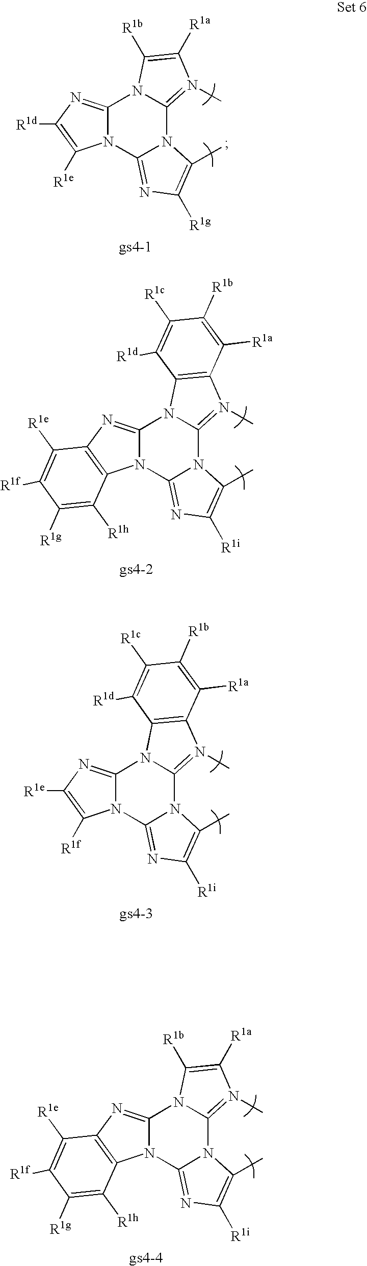
wherein:

wherein:

wherein:

wherein:


wherein:


wherein:
| TABLE 1 | |||||||
| Cal. | Cal. | Cal. | Cal. | Cal. | Cal. | ||
| HOMO | LUMO | Gap | Dipole | S1 | T1 | ||
| Entry | Compounds | (ev) | (ev) | (ev) | (Debye) | (nm) | (nm) |
| 1 |
 |
−4.73 | −1.17 | 3.57 | 4.72 | 446 | 475 |
| 2 |
 |
−4.99 | −1.33 | 3.65 | 0.21 | 434 | 470 |
| 3 |
 |
−5.11 | −1.21 | 3.90 | 3.44 | 394 | 477 |
| 4 |
 |
−4.88 | −1.42 | 3.46 | 3.06 | 465 | 493 |
| 5 |
 |
−5.17 | −1.47 | 3.69 | 11.40 | 427 | 467 |
| 6 |
 |
−4.83 | −0.93 | 3.90 | 8.28 | 425 | 490 |
| 7 |
 |
−4.52 | −0.77 | 3.75 | 11.91 | 396 | 493 |
| 8 |
 |
−4.96 | −1.04 | 3.92 | 18.02 | 401 | 485 |
| 9 |
 |
−4.92 | −1.43 | 3.49 | 18.06 | 414 | 488 |
| 10 |
 |
−5.15 | −1.65 | 3.49 | 11.79 | 444 | 479 |
| 11 |
 |
−4.38 | −0.81 | 3.57 | 2.90 | 447 | 471 |
| 12 |
 |
−4.93 | −1.62 | 3.31 | 14.71 | 455 | 492 |
| 13 |
 |
−4.51 | −0.99 | 3.52 | 5.76 | 459 | 495 |
| 14 |
 |
−5.45 | −1.98 | 3.47 | 4.41 | 454 | 478 |
| 15 |
 |
−4.55 | −0.94 | 3.61 | 8.96 | 442 | 478 |
| 16 |
 |
−4.58 | −0.96 | 3.62 | 4.96 | 443 | 476 |
| 17 |
 |
−4.61 | −1.09 | 3.52 | 6.18 | 450 | 480 |
| 18 |
 |
−4.90 | −1.54 | 3.36 | 4.74 | 476 | 552 |
| 19 |
 |
−4.94 | −1.74 | 3.19 | 2.12 | 485 | 613 |
| 20 |
 |
−5.13 | −2.01 | 3.12 | 1.52 | 511 | 540 |
| 21 |
 |
−4.88 | −1.30 | 3.58 | 3.14 | 450 | 479 |
| 22 |
 |
−4.53 | −1.01 | 3.52 | 8.65 | 454 | 478 |
| 23 |
 |
−4.67 | −1.06 | 3.60 | 8.96 | 447 | 481 |
| 24 |
 |
−4.82 | −1.36 | 3.46 | 3.33 | 454 | 517 |
| 25 |
 |
−5.28 | −1.60 | 3.68 | 10.11 | 435 | 473 |
| 26 |
 |
−5.21 | −1.64 | 3.57 | 10.21 | 439 | 510 |
| 27 |
 |
−5.25 | −1.61 | 3.64 | 9.35 | 440 | 476 |
| 28 |
 |
−5.13 | −2.45 | 2.68 | 2.31 | 590 | 674 |
| 29 |
 |
−5.10 | −1.37 | 3.74 | 16.13 | 430 | 474 |
| 30 |
 |
−5.25 | −1.61 | 3.63 | 10.28 | 438 | 481 |
| 31 |
 |
−4.66 | −1.17 | 3.49 | 4.35 | 448 | 479 |
| 32 |
 |
−4.50 | −0.91 | 3.59 | 7.98 | 444 | 480 |
| 33 |
 |
−4.33 | −0.67 | 3.66 | 8.45 | 433 | 474 |
| 34 |
 |
−4.38 | −0.80 | 3.57 | 2.77 | 447 | 471 |
| 35 |
 |
−4.64 | −1.31 | 3.33 | 7.04 | 479 | 486 |
| 36 |
 |
−4.88 | −1.47 | 3.41 | 1.43 | 456 | 483 |
| 37 |
 |
−5.02 | −1.90 | 3.12 | 2.82 | 471 | 486 |
| 38 |
 |
−4.79 | −1.32 | 3.47 | 0.10 | 456 | 484 |
| 39 |
 |
−4.85 | −1.40 | 3.45 | 3.14 | 458 | 487 |
| 40 |
 |
−4.66 | −1.11 | 3.55 | 5.48 | 445 | 478 |
| 41 |
 |
−4.67 | −1.12 | 3.55 | 5.76 | 448 | 477 |
| 42 |
 |
−4.54 | −1.08 | 3.46 | 7.01 | 460 | 484 |
| 43 |
 |
−4.52 | −1.05 | 3.47 | 2.72 | 462 | 483 |
| 44 |
 |
−5.11 | −1.62 | 3.49 | 10.59 | 453 | 478 |
| 45 |
 |
−4.75 | −1.45 | 3.30 | 5.02 | 487 | 518 |
| 46 |
 |
−5.08 | −2.18 | 2.90 | 13.63 | 531 | 623 |
| 47 |
 |
−5.22 | −1.76 | 3.46 | 5.70 | 467 | 485 |
| 48 |
 |
−4.87 | −1.37 | 3.50 | 3.13 | 468 | 481 |
| 49 |
 |
−4.56 | −0.97 | 3.85 | 5.02 | 442 | 474 |
| 50 |
 |
−4.57 | −0.97 | 3.60 | 5.03 | 441 | 477 |
| 51 |
 |
−4.57 | −1.10 | 3.47 | 4.94 | 447 | 480 |
| 52 |
 |
−4.51 | −1.06 | 3.45 | 4.36 | 447 | 479 |
| 53 |
 |
−4.45 | −1.01 | 3.44 | 4.77 | 441 | 478 |
| 54 |
 |
−4.58 | −0.98 | 3.60 | 4.92 | 442 | 476 |
| 55 |
 |
−4.65 | −1.04 | 3.60 | 5.43 | 442 | 476 |
| 56 |
 |
−4.52 | −0.92 | 3.60 | 6.23 | 442 | 476 |
| 57 |
 |
−4.45 | −0.85 | 3.60 | 7.72 | 442 | 476 |
| 58 |
 |
−4.49 | −0.87 | 3.62 | 5.45 | 438 | 474 |
| 59 |
 |
−5.27 | −1.91 | 3.36 | 2.99 | 478 | 501 |
| 60 |
 |
−5.75 | −2.39 | 3.37 | 4.27 | 476 | 507 |
| 61 |
 |
−5.22 | −1.46 | 3.77 | 0.08 | 427 | 463 |
| 62 |
 |
−5.68 | −2.05 | 3.64 | 4.12 | 441 | 467 |
| 63 |
 |
−5.88 | −2.40 | 3.48 | 3.83 | 460 | 472 |
| 64 |
 |
−4.74 | −1.65 | 3.08 | 9.02 | 469 | 484 |
| 65 |
 |
−5.37 | −1.69 | 3.68 | 8.08 | 434 | 472 |
| 66 |
 |
−5.32 | −1.33 | 4.00 | 0.25 | 389 | 476 |
| 67 |
 |
−4.24 | −0.65 | 3.60 | 3.14 | 449 | 480 |
| 68 |
 |
−4.28 | −0.71 | 3.57 | 3.23 | 454 | 479 |
| 69 |
 |
−4.82 | −1.20 | 3.62 | 1.03 | 440 | 475 |
| 70 |
 |
−4.95 | −1.36 | 3.59 | 0.28 | 441 | 476 |
| 71 |
 |
−4.65 | −1.18 | 3.47 | 5.66 | 442 | 476 |
| 72 |
 |
−4.44 | −0.82 | 3.62 | 5.50 | 439 | 479 |
| 73 |
 |
−5.19 | −1.79 | 3.40 | 0.50 | 468 | 483 |
| 74 |
 |
−5.16 | −1.64 | 3.51 | 7.01 | 452 | 479 |
| 75 |
 |
−4.49 | −0.80 | 3.69 | 6.62 | 434 | 475 |
| 76 |
 |
−5.01 | −0.97 | 4.04 | 3.07 | 375 | 446 |
| 77 |
 |
−5.46 | −1.44 | 4.01 | 2.34 | 377 | 448 |
| 78 |
 |
−5.22 | −1.24 | 3.97 | 8.24 | 382 | 451 |
| 79 |
 |
−5.10 | −0.99 | 4.11 | 10.38 | 400 | 465 |
| 80 |
 |
−5.84 | −1.96 | 3.88 | 0.91 | 409 | 529 |
| 81 |
 |
−5.30 | −1.48 | 3.82 | 1.26 | 412 | 542 |
| 82 |
 |
−5.19 | −1.18 | 4.01 | 2.09 | 377 | 449 |
| 83 |
 |
−5.33 | −1.31 | 4.02 | 2.45 | 376 | 448 |
| 84 |
 |
−5.34 | −1.53 | 3.82 | 1.53 | 403 | 463 |
| 85 |
 |
−5.40 | −1.70 | 3.70 | 1.70 | 419 | 480 |
| 86 |
 |
−5.39 | −1.52 | 3.87 | 3.36 | 428 | 461 |
| 87 |
 |
−5.31 | −1.61 | 3.70 | 7.43 | 423 | 473 |
| 88 |
 |
−4.85 | −1.17 | 3.68 | 2.60 | 427 | 485 |
| 89 |
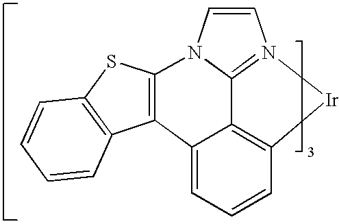 |
−4.88 | −1.33 | 3.55 | 2.32 | 442 | 496 |
| 90 |
 |
−5.46 | −1.66 | 3.80 | 0.78 | 412 | 494 |
| 91 |
 |
−5.28 | −1.57 | 3.71 | 2.81 | 419 | 479 |
| 92 |
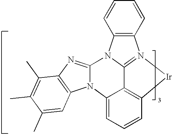 |
−5.24 | −1.53 | 3.71 | 1.74 | 421 | 479 |
| 93 |
 |
−5.19 | −1.51 | 3.68 | 2.80 | 432 | 483 |
| 94 |
 |
−6.19 | −2.54 | 3.66 | 9.25 | 429 | 472 |
| 95 |
 |
−5.86 | −2.11 | 3.74 | 10.90 | 426 | 460 |
| 96 |
 |
−5.06 | −1.11 | 3.95 | 2.69 | 381 | 456 |
| 97 |
 |
−5.22 | −1.45 | 3.76 | 0.68 | 397 | 473 |
| 98 |
 |
−4.91 | −0.96 | 3.95 | 2.51 | 383 | 460 |
| 99 |
 |
— | — | — | — | — | — |
| 100 |
 |
−5.13 | −1.39 | 3.74 | 2.52 | 422 | 472 |
| 101 |
 |
||||||

where n=1, 2 or 3; R1a, R1b, R1c, R1d, R1e, R1g, R1h, and R1i are each, independently, H, hydrocarbyl, heteroatom substituted hydrocarbyl, cyano, fluoro, OR2a, SR2a, NR2aR2b, BR2aR2b, or SiR2aR2bR2c, where R2a-c are each, independently, hydrocarbyl or heteroatom substituted hydrocarbyl, and where any two of R1a and R2a-c may be linked to form a saturated or unsaturated, aromatic or non-aromatic ring. X—Y is an ancillary ligand. The complex of Formula I is illustrated in

where Ra, Rb and Rc are independently H, alkyl or aryl, where at least one of Ra and Rb is an alkyl or aryl; and where Ra, Rb and Rc can join to form fused rings. Preferably, at least one of Ra and Rb is an alkyl. The steric bulk provided by an alkyl or aryl in the Ra and/or Rb position causes the aryl in the R1b position to twist. Preferably, the twisting results in a complex where R1b is an aryl group with a dihedral angle of more than 70 degrees from the imidazole ring. Ra and Rb may both be alkyl or aryl, which may result in more twisting. Methyl is a preferred alkyl for the Ra and/or Rb positions due to ease of fabrication. Isopropyl is a preferred alkyl for the Ra and/or Rb positions due to a combination of added steric bulk relative to methyl. Preferred compounds having a “twisted aryl” in the R1b position include es45 and es46:


| TABLE 1 |
| Device example structures |
| Device | EML | thickness | ETL2 | ETL1 |
| Example | HIL | HTL | Host | Compound | Doping % | (nm) | (nm) | (nm) |
| Comparative | CuPc | NPD | CBP | A | 9 | 30 | BAlq (40) | none |
| 1 | ||||||||
| 1 | CuPc | NPD | mCBP | es1 | 9 | 30 | BAlq (40) | none |
| 2 | CuPc | NPD | mCBP | es6 | 9 | 30 | BAlq (40) | none |
| 3 | CuPc | NPD | mCBP | es8 | 9 | 30 | BAlq (40) | none |
| 4 | CuPc | NPD | mCBP | es9 | 9 | 30 | BAlq (40) | none |
| 5 | CuPc | NPD | mCBP | es13 | 9 | 30 | BAlq (40) | none |
| 6 | CuPc | NPD | mCBP | es14 | 9 | 30 | BAlq (40) | none |
| 7 | CuPc | NPD | mCBP | es16 | 9 | 30 | BAlq (40) | none |
| 8 | CuPc | NPD | mCBP | es17 | 9 | 30 | BAlq (40) | none |
| 9 | CuPc | NPD | mCBP | es19 | 9 | 30 | BAlq (40) | none |
| 10 | Ir(3-Meppy)3 | NPD | mCBP | es20 | 9 | 30 | BAlq (40) | none |
| 11 | CuPc | NPD | CBP | es4 | 6 | 30 | HPT (5) | Alq3 (45) |
| 12 | Ir(3-Meppy)3 | none | mCBP | es20 | 15 | 60 | mCBP (5) | Alq3 (20) |
| 13 | es20 | none | mCBP | es20 | 15 | 60 | mCBP (5) | Alq3 (20) |
| 14 | CuPc | none | mCBP | es38 | 15 | 80 | mCBP (5) | Alq3 (20) |
| 15 | CuPc | none | mCBP | es38 | 15 | 60 | mCBP (5) | Alq3 (20) |
| 16 | Ir(3-Meppy)3 | none | mCBP | es38 | 15 | 80 | mCBP (5) | Alq3 (20) |
| 17 | Ir(3-Meppy)3 | none | mCBP | es38 | 15 | 60 | mCBP (5) | Alq3 (20) |
| 18 | LG101 | NPD | mCBP | es38 | 9 | 20 | mCBP (5) | Alq3 (20) |
| 19 | Ir(3-Meppy)3 | NPD | mCBP | es43 | 9 | 30 | mCBP (5) | Alq3 (40) |
| 20 | Ir(3-Meppy)3 | NPD | mCBP | es46 | 9 | 30 | mCBP (5) | Alq3 (40) |
| 21 | Ir(3-Meppy)3 | NPD | mCBP | es49 | 9 | 30 | mCBP (5) | Alq3 (40) |
| 22 | Ir(3-Meppy)3 | NPD | mCBP | es45 | 9 | 30 | none | Alq3 (40) |
| TABLE 2 |
| Device properties of device examples |
| Device | J = 10 mA/cm2 | At L = 1000 cd/m2 | Stability |
| Example | Emmax(nm) | CIE x | CIE y | V (V) | LE (cd/A) | EQE (%) | PE (Im/W) | L0 (cd/m2) | T1/2 (hr) | Figure |
| Comparative | 472 | 0.170 | 0.380 | 10.0 | 10.5 | 4.7 | 3.30 | 100 | 170 | no figure |
| 1 | ||||||||||
| 1 | 460 | 0.150 | 0.210 | 14.0 | 4.116 | 2.672 | 0.92 | 450 | 273 | 3 |
| 2 | 460 | 0.150 | 0.190 | >15 | <2.5 | <1.7 | <0.5 | 270 | 700 | 4 |
| 3 | 460 | 0.140 | 0.190 | 14.6 | 4.433 | 3.079 | 0.95 | 470 | 400 | 5 |
| 4 | 459 | 0.140 | 0.180 | 14.4 | 4.13 | 3.01 | 0.90 | 420 | 210 | 6 |
| 5 | 462 | 0.14 | 0.18 | 13.4 | 6.836 | 4.573 | 1.60 | 680 | 310 | 7 |
| 6 | 460 | 0.15 | 0.21 | 14.4 | 6.352 | 4.169 | 1.39 | 1240 | 115 | 8 |
| 7 | 460 | 0.150 | 0.210 | 13.8 | 5.07 | 3.56 | 1.14 | 525 | 320 | 9 |
| 8 | 464 | 0.16 | 0.28 | 12.8 | 9.387 | 4.957 | 2.30 | 938 | 104 | 10 |
| 9 | 464 | 0.16 | 0.28 | >15 | <2 | <1.2 | <.4 | not tested | not tested | 11 |
| 10 | 462 | 0.150 | 0.240 | 12.0 | 13.378 | 8.042 | 3.50 | 2300 | 106 | 12 |
| 11 | 498 | 0.250 | 0.590 | 9.0 | 13.4 | 4.5 | 4.70 | 4300 | 340 | 13 |
| 12 | 462 | 0.160 | 0.250 | 10.4 | 12.26 | 7.07 | 3.70 | 500 | 2200 | 15 |
| 13 | 462 | 0.160 | 0.240 | 13.0 | 9.534 | 5.603 | 2.30 | 500 | 2500 | 16 |
| 14 | 462 | 0.150 | 0.260 | 16.4 | 7.9 | 4.5 | 1.51 | 500 | >10,000 | 17 |
| 15 | 462 | 0.15 | 0.22 | 13.3 | 6.5 | 4 | 1.54 | 1000 | 1000 | 18 |
| 16 | 462 | 0.160 | 0.270 | 14.9 | 12.7 | 6.9 | 2.67 | 500 | >10,000 | 19 |
| 17 | 462 | 0.160 | 0.240 | 11.9 | 11.7 | 6.7 | 3.07 | 1000 | 1400 | 20 |
| 18 | 462 | 0.15 | 0.200 | 7.2 | 10.1 | 6.8 | 4.40 | 1000 | 200 | 21 |
| 19 | 464 | 0.15 | 0.24 | 8.2 | 19.9 | 12.2 | 7.60 | 1,000 | 270 | no figure |
| 20 | 462 | 0.15 | 0.25 | 9.5 | 14 | 8.1 | 4.60 | 2,000 | 220 | no figure |
| 21 | 462 | 0.15 | 0.23 | 6.9 | 11.5 | 7.1 | 5.20 | 2,000 | 40 | no figure |
| 22 | 460 | 0.15 | 0.24 | 9.3 | 10.8 | 6.5 | 3.70 | 2,000 | 81 | no figure |


| TABLE 3 |
| Effect on color by methyl substitution on the imidazole ring |
 |
| Emission | CIE | |||||
| Cpd # | R1b | R1a | Max. (nm) | (Soln. PL) | ||
| es1 | H | H | 462 | 0.17, 0.26 | ||
| | H | Methyl | 460 | 0.17, 0.28 | ||
| es44 | Methyl | Methyl | 470 | 0.19, 0.35 | ||

Proposed Energy Diagram of es1 and es43.


Step 1: Ligand Synthesis

Step 1: Ligand Synthesis

Step 1: Ligand Synthesis
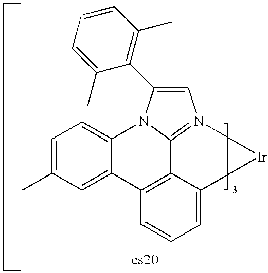


0.389 mmol) and 30 drops of tridecane. The flask was evacuated and re-filled refilled with nitrogen three times and then heated to 240 C for 26 h. The resultant mixture was dissolved in methylene chloride and subjected to silica gel column chromatography to afford es101, the structure of which was confirmed by mass spectrometry.


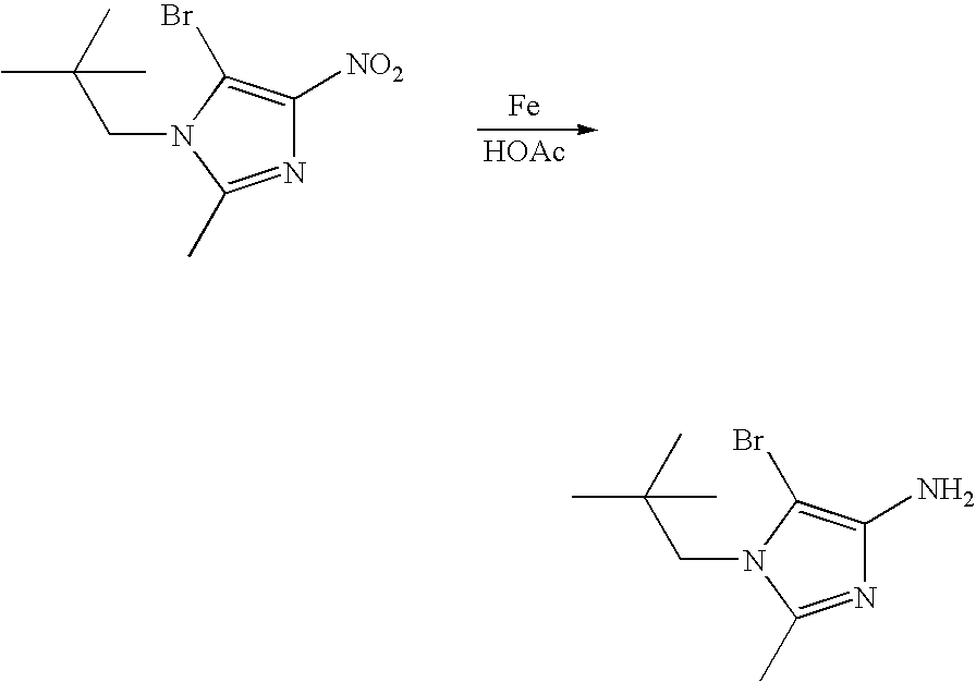


10.

Claims (44)


Priority Applications (5)
| Application Number | Priority Date | Filing Date | Title |
|---|---|---|---|
| US12/044,605 US8142909B2 (en) | 2006-02-10 | 2008-03-07 | Blue phosphorescent imidazophenanthridine materials |
| PCT/US2008/056297 WO2008156879A1 (en) | 2007-06-20 | 2008-03-07 | Blue phosphorescent imidazophenanthridine materials |
| TW107117543A TWI683884B (en) | 2007-06-20 | 2008-05-05 | Blue phosphorescent imidazophenanthridine materials |
| TW108131926A TWI743556B (en) | 2007-06-20 | 2008-05-05 | Organic emissive layer and organic light emitting device comprising the same |
| TW097116557A TWI637955B (en) | 2007-06-20 | 2008-05-05 | Blue phosphorescent imidazophenanthridine materials |
Applications Claiming Priority (6)
| Application Number | Priority Date | Filing Date | Title |
|---|---|---|---|
| US77215406P | 2006-02-10 | 2006-02-10 | |
| US85682406P | 2006-11-03 | 2006-11-03 | |
| US87419006P | 2006-12-11 | 2006-12-11 | |
| US11/704,585 US7915415B2 (en) | 2006-02-10 | 2007-02-09 | Metal complexes of cyclometallated imidazo[1,2-f]phenanthridine and diimidazo[1,2-a:1′,2′-c]quinazoline ligands and isoelectronic and benzannulated analogs thereof |
| US93664307P | 2007-06-20 | 2007-06-20 | |
| US12/044,605 US8142909B2 (en) | 2006-02-10 | 2008-03-07 | Blue phosphorescent imidazophenanthridine materials |
Related Parent Applications (1)
| Application Number | Title | Priority Date | Filing Date |
|---|---|---|---|
| US11/704,585 Continuation-In-Part US7915415B2 (en) | 2006-02-10 | 2007-02-09 | Metal complexes of cyclometallated imidazo[1,2-f]phenanthridine and diimidazo[1,2-a:1′,2′-c]quinazoline ligands and isoelectronic and benzannulated analogs thereof |
Publications (2)
| Publication Number | Publication Date |
|---|---|
| US20080297033A1 US20080297033A1 (en) | 2008-12-04 |
| US8142909B2 true US8142909B2 (en) | 2012-03-27 |
Family
ID=39684211
Family Applications (1)
| Application Number | Title | Priority Date | Filing Date |
|---|---|---|---|
| US12/044,605 Active 2029-10-31 US8142909B2 (en) | 2006-02-10 | 2008-03-07 | Blue phosphorescent imidazophenanthridine materials |
Country Status (3)
| Country | Link |
|---|---|
| US (1) | US8142909B2 (en) |
| TW (3) | TWI637955B (en) |
| WO (1) | WO2008156879A1 (en) |
Cited By (17)
| Publication number | Priority date | Publication date | Assignee | Title |
|---|---|---|---|---|
| US20100148663A1 (en) * | 2008-12-12 | 2010-06-17 | Universal Display Corporation | Blue Emitter with High Efficiency Based on Imidazo[1,2-f] Phenanthridine Iridium Complexes |
| US20110073849A1 (en) * | 2006-02-10 | 2011-03-31 | Knowles David B | METAL COMPLEXES OF CYCLOMETALLATED IMIDAZO[1,2-f ]PHENANTHRIDINE AND DIIMIDAZO[1,2-a:1',2'-c ]QUNIAZOLINE LIGANDS AND ISOELECTRONIC AND BENZANNULATED ANALOGS THEREOF |
| US20110101854A1 (en) * | 2009-11-02 | 2011-05-05 | Semiconductor Energy Laboratory Co., Ltd. | Organometallic Complex, Light-Emitting Element, Display Device, Electronic Device, and Lighting Device |
| US20110220882A1 (en) * | 2010-03-15 | 2011-09-15 | Semiconductor Energy Laboratory Co., Ltd. | Organometallic Complex, Light-Emitting Element, Display Device, Electronic Device, and Lighting Device |
| US20140191227A1 (en) * | 2011-08-30 | 2014-07-10 | Konica Minolta, Inc. | Organic electroluminescence element |
| US8784690B2 (en) | 2010-08-20 | 2014-07-22 | Rhodia Operations | Polymer compositions, polymer films, polymer gels, polymer foams, and electronic devices containing such films, gels and foams |
| EP2887417A2 (en) | 2013-12-17 | 2015-06-24 | The Regents Of The University Of Michigan | Extended OLED operational lifetime through phosphorescent dopant profile mangement |
| US9155158B2 (en) | 2011-04-01 | 2015-10-06 | Semiconductor Energy Laboratory Co., Ltd. | Organometallic complex, light-emitting element, display device, electronic device, and lighting device |
| US20150295192A1 (en) * | 2014-04-14 | 2015-10-15 | Universal Display Corporation | Organic Electroluminescent Materials and Devices |
| US20150295190A1 (en) * | 2014-04-14 | 2015-10-15 | Universal Display Corporation | Organic Electroluminescent Materials and Devices |
| US9512123B2 (en) | 2014-05-09 | 2016-12-06 | Pimera, Inc. | Compositions, uses and methods for making them |
| US9634266B2 (en) | 2013-12-25 | 2017-04-25 | Industrial Technology Research Institute | Organic metal compound, organic light-emitting device, and lighting device employing the same |
| US9758518B2 (en) | 2015-03-04 | 2017-09-12 | Pimera, Inc. | Compositions, uses and methods for making them |
| US10164198B2 (en) | 2015-02-05 | 2018-12-25 | Samsung Electronics Co., Ltd. | Organometallic compound, composition containing organometallic compound, and organic light-emitting device including the same |
| US10326086B2 (en) | 2015-02-06 | 2019-06-18 | Samsung Electronics Co., Ltd. | Organometallic compound, composition containing the organometallic compound, and organic light-emitting device including the organometallic compound or composition |
| US10411199B2 (en) | 2012-12-12 | 2019-09-10 | Samsung Electronics Co., Ltd. | Organometallic complexes, and organic electroluminescent device and display using the same |
| US11912706B2 (en) | 2017-03-28 | 2024-02-27 | Pimera, Inc. | Crystal forms of a POL1 inhibitor |
Families Citing this family (608)
| Publication number | Priority date | Publication date | Assignee | Title |
|---|---|---|---|---|
| US9070884B2 (en) | 2005-04-13 | 2015-06-30 | Universal Display Corporation | Hybrid OLED having phosphorescent and fluorescent emitters |
| US8586204B2 (en) | 2007-12-28 | 2013-11-19 | Universal Display Corporation | Phosphorescent emitters and host materials with improved stability |
| US9051344B2 (en) | 2005-05-06 | 2015-06-09 | Universal Display Corporation | Stability OLED materials and devices |
| US8007927B2 (en) | 2007-12-28 | 2011-08-30 | Universal Display Corporation | Dibenzothiophene-containing materials in phosphorescent light emitting diodes |
| US8142909B2 (en) * | 2006-02-10 | 2012-03-27 | Universal Display Corporation | Blue phosphorescent imidazophenanthridine materials |
| US20130032785A1 (en) | 2011-08-01 | 2013-02-07 | Universal Display Corporation | Materials for organic light emitting diode |
| US9130177B2 (en) | 2011-01-13 | 2015-09-08 | Universal Display Corporation | 5-substituted 2 phenylquinoline complexes materials for light emitting diode |
| JP5638246B2 (en) | 2007-03-08 | 2014-12-10 | ユニバーサル ディスプレイ コーポレイション | Phosphorescent material |
| JP5482201B2 (en) | 2007-05-16 | 2014-05-07 | コニカミノルタ株式会社 | Organic electroluminescence element, display device and lighting device |
| WO2008142976A1 (en) * | 2007-05-16 | 2008-11-27 | Konica Minolta Holdings, Inc. | Organic electroluminescence element, display device, illuminating device and organic electroluminescence element material |
| TWI511964B (en) | 2007-08-08 | 2015-12-11 | Universal Display Corp | Benzo-fused thiophene/triphenylen hybrid materials |
| TWI562975B (en) | 2007-08-08 | 2016-12-21 | Universal Display Corp | Single triphenylene chromophores in phosphorescent light emitting diodes |
| US8476822B2 (en) | 2007-11-09 | 2013-07-02 | Universal Display Corporation | Saturated color organic light emitting devices |
| US8815411B2 (en) | 2007-11-09 | 2014-08-26 | The Regents Of The University Of Michigan | Stable blue phosphorescent organic light emitting devices |
| WO2009073245A1 (en) | 2007-12-06 | 2009-06-11 | Universal Display Corporation | Light-emitting organometallic complexes |
| WO2009150150A1 (en) * | 2008-06-10 | 2009-12-17 | Basf Se | Novel transition metal complex and use thereof in organic light-emitting diodes - iii |
| KR20170070273A (en) | 2008-06-10 | 2017-06-21 | 유디씨 아일랜드 리미티드 | Deuterated transition metal complex and use thereof in organic light-emitting diodes ⅴ |
| JP5591800B2 (en) | 2008-06-30 | 2014-09-17 | ユニバーサル・ディスプレイ・コーポレーション | Hole transport material containing triphenylene |
| WO2010027583A1 (en) | 2008-09-03 | 2010-03-11 | Universal Display Corporation | Phosphorescent materials |
| US9034483B2 (en) | 2008-09-16 | 2015-05-19 | Universal Display Corporation | Phosphorescent materials |
| JP5272608B2 (en) * | 2008-09-20 | 2013-08-28 | コニカミノルタ株式会社 | Organic electroluminescence element, display device, and lighting device |
| KR101678235B1 (en) | 2008-09-25 | 2016-11-21 | 유니버셜 디스플레이 코포레이션 | Organoselenium materials and their uses in organic light emitting devices |
| US8368062B2 (en) | 2008-11-03 | 2013-02-05 | Lg Chem, Ltd. | Nitrogen-containing heterocyclic compound and organic electronic device using the same |
| KR101843201B1 (en) * | 2008-11-11 | 2018-03-28 | 유니버셜 디스플레이 코포레이션 | Phosphorescent emitters |
| US9067947B2 (en) | 2009-01-16 | 2015-06-30 | Universal Display Corporation | Organic electroluminescent materials and devices |
| DE102009007038A1 (en) | 2009-02-02 | 2010-08-05 | Merck Patent Gmbh | metal complexes |
| KR101398711B1 (en) | 2009-02-27 | 2014-05-27 | 주식회사 엘지화학 | Nitrogen containing compound and organic electronic device using the same |
| JP5600884B2 (en) * | 2009-03-17 | 2014-10-08 | コニカミノルタ株式会社 | ORGANIC ELECTROLUMINESCENT ELEMENT, ORGANIC ELECTROLUMINESCENT ELEMENT MATERIAL, DISPLAY DEVICE AND LIGHTING DEVICE |
| US8709615B2 (en) | 2011-07-28 | 2014-04-29 | Universal Display Corporation | Heteroleptic iridium complexes as dopants |
| US11910700B2 (en) | 2009-03-23 | 2024-02-20 | Universal Display Corporation | Heteroleptic iridium complexes as dopants |
| US8722205B2 (en) | 2009-03-23 | 2014-05-13 | Universal Display Corporation | Heteroleptic iridium complex |
| TWI687408B (en) | 2009-04-28 | 2020-03-11 | 美商環球展覽公司 | Iridium complex with methyl-D3 substitution |
| US8586203B2 (en) | 2009-05-20 | 2013-11-19 | Universal Display Corporation | Metal complexes with boron-nitrogen heterocycle containing ligands |
| JP4523992B1 (en) | 2009-07-31 | 2010-08-11 | 富士フイルム株式会社 | Organic electroluminescence device |
| JP5382887B2 (en) | 2009-08-27 | 2014-01-08 | 独立行政法人産業技術総合研究所 | Iridium complex and light-emitting material comprising the compound |
| JP4542607B1 (en) | 2009-08-31 | 2010-09-15 | 富士フイルム株式会社 | Method for sublimation purification of iridium complex and method for producing organic electroluminescent device |
| JP4564588B1 (en) * | 2009-08-31 | 2010-10-20 | 富士フイルム株式会社 | Material for organic electroluminescence device and organic electroluminescence device |
| JP4551480B1 (en) | 2009-08-31 | 2010-09-29 | 富士フイルム株式会社 | Organic electroluminescence device |
| JP5779318B2 (en) | 2009-08-31 | 2015-09-16 | ユー・ディー・シー アイルランド リミテッド | Organic electroluminescence device |
| JP4599469B1 (en) * | 2009-08-31 | 2010-12-15 | 富士フイルム株式会社 | Organic electroluminescent element material and organic electroluminescent element |
| JP5457907B2 (en) | 2009-08-31 | 2014-04-02 | ユー・ディー・シー アイルランド リミテッド | Organic electroluminescence device |
| JP4474492B1 (en) | 2009-08-31 | 2010-06-02 | 富士フイルム株式会社 | Material for organic electroluminescence device and organic electroluminescence device |
| JP5926477B2 (en) | 2009-08-31 | 2016-05-25 | ユー・ディー・シー アイルランド リミテッド | Method for producing metal complex compound and organic electroluminescent device |
| JP5770441B2 (en) | 2009-09-30 | 2015-08-26 | ユー・ディー・シー アイルランド リミテッド | Material for organic electroluminescence device and organic electroluminescence device |
| JP5627896B2 (en) * | 2009-09-30 | 2014-11-19 | ユー・ディー・シー アイルランド リミテッド | Organic electroluminescence device |
| US8545996B2 (en) | 2009-11-02 | 2013-10-01 | The University Of Southern California | Ion-pairing soft salts based on organometallic complexes and their applications in organic light emitting diodes |
| US8580394B2 (en) | 2009-11-19 | 2013-11-12 | Universal Display Corporation | 3-coordinate copper(I)-carbene complexes |
| KR101288574B1 (en) * | 2009-12-02 | 2013-07-22 | 제일모직주식회사 | Filler for filling a gap and method for manufacturing semiconductor capacitor using the same |
| JP5463897B2 (en) * | 2009-12-18 | 2014-04-09 | コニカミノルタ株式会社 | ORGANIC ELECTROLUMINESCENT ELEMENT, ORGANIC ELECTROLUMINESCENT ELEMENT MATERIAL, DISPLAY DEVICE AND LIGHTING DEVICE |
| JP6014304B2 (en) * | 2010-01-15 | 2016-10-25 | ユー・ディー・シー アイルランド リミテッド | Organic electroluminescence device |
| US8288187B2 (en) | 2010-01-20 | 2012-10-16 | Universal Display Corporation | Electroluminescent devices for lighting applications |
| US9156870B2 (en) * | 2010-02-25 | 2015-10-13 | Universal Display Corporation | Phosphorescent emitters |
| US9175211B2 (en) * | 2010-03-03 | 2015-11-03 | Universal Display Corporation | Phosphorescent materials |
| US8963132B2 (en) | 2010-03-25 | 2015-02-24 | Universal Display Corporation | Solution processable doped triarylamine hole injection materials |
| JP5724204B2 (en) * | 2010-04-07 | 2015-05-27 | コニカミノルタ株式会社 | Organic electroluminescence element, display device, and lighting device |
| JP5646733B2 (en) | 2010-04-28 | 2014-12-24 | ユニバーサル ディスプレイ コーポレイション | Premixed material deposition |
| US8968887B2 (en) | 2010-04-28 | 2015-03-03 | Universal Display Corporation | Triphenylene-benzofuran/benzothiophene/benzoselenophene compounds with substituents joining to form fused rings |
| US8742657B2 (en) | 2010-06-11 | 2014-06-03 | Universal Display Corporation | Triplet-Triplet annihilation up conversion (TTA-UC) for display and lighting applications |
| US8673458B2 (en) | 2010-06-11 | 2014-03-18 | Universal Display Corporation | Delayed fluorescence OLED |
| JP5846119B2 (en) | 2010-06-17 | 2016-01-20 | コニカミノルタ株式会社 | ORGANIC ELECTROLUMINESCENT MATERIAL, ORGANIC ELECTROLUMINESCENT ELEMENT, METHOD FOR PRODUCING ORGANIC ELECTROLUMINESCENT ELEMENT, DISPLAY DEVICE AND LIGHTING DEVICE |
| US9435021B2 (en) | 2010-07-29 | 2016-09-06 | University Of Southern California | Co-deposition methods for the fabrication of organic optoelectronic devices |
| KR101925158B1 (en) | 2010-08-02 | 2018-12-04 | 가부시키가이샤 한도오따이 에네루기 켄큐쇼 | Triazole derivative, heterocyclic compound, light-emitting element, light-emitting device, electronic device and lighting device |
| TW201223956A (en) * | 2010-08-13 | 2012-06-16 | Solvay | Light emitting materials for electronics |
| EP2423214A1 (en) * | 2010-08-13 | 2012-02-29 | Solvay SA | Light emitting materials for Electronics |
| US9954180B2 (en) | 2010-08-20 | 2018-04-24 | Universal Display Corporation | Bicarbazole compounds for OLEDs |
| US8932734B2 (en) | 2010-10-08 | 2015-01-13 | Universal Display Corporation | Organic electroluminescent materials and devices |
| US8269317B2 (en) | 2010-11-11 | 2012-09-18 | Universal Display Corporation | Phosphorescent materials |
| US20120138906A1 (en) | 2010-12-07 | 2012-06-07 | The University of Southern California USC Stevens Institute for Innovation | Capture agents for unsaturated metal complexes |
| US20130331577A1 (en) | 2010-12-23 | 2013-12-12 | Solvay Sa | Preparation of a fac-isomer for a tris homoleptic metal complex |
| US10008677B2 (en) | 2011-01-13 | 2018-06-26 | Universal Display Corporation | Materials for organic light emitting diode |
| US8415031B2 (en) | 2011-01-24 | 2013-04-09 | Universal Display Corporation | Electron transporting compounds |
| US8748011B2 (en) | 2011-02-23 | 2014-06-10 | Universal Display Corporation | Ruthenium carbene complexes for OLED material |
| US9005772B2 (en) | 2011-02-23 | 2015-04-14 | Universal Display Corporation | Thioazole and oxazole carbene metal complexes as phosphorescent OLED materials |
| US8563737B2 (en) | 2011-02-23 | 2013-10-22 | Universal Display Corporation | Methods of making bis-tridentate carbene complexes of ruthenium and osmium |
| CN115448957A (en) | 2011-02-23 | 2022-12-09 | 通用显示公司 | Novel tetradentate platinum complexes |
| US8492006B2 (en) | 2011-02-24 | 2013-07-23 | Universal Display Corporation | Germanium-containing red emitter materials for organic light emitting diode |
| JP5747736B2 (en) * | 2011-03-01 | 2015-07-15 | コニカミノルタ株式会社 | Organic electroluminescence element, display device and lighting device |
| US8883322B2 (en) | 2011-03-08 | 2014-11-11 | Universal Display Corporation | Pyridyl carbene phosphorescent emitters |
| US8580399B2 (en) | 2011-04-08 | 2013-11-12 | Universal Display Corporation | Substituted oligoazacarbazoles for light emitting diodes |
| US8432095B2 (en) | 2011-05-11 | 2013-04-30 | Universal Display Corporation | Process for fabricating metal bus lines for OLED lighting panels |
| US8564192B2 (en) | 2011-05-11 | 2013-10-22 | Universal Display Corporation | Process for fabricating OLED lighting panels |
| US8927308B2 (en) | 2011-05-12 | 2015-01-06 | Universal Display Corporation | Method of forming bus line designs for large-area OLED lighting |
| US9212197B2 (en) | 2011-05-19 | 2015-12-15 | Universal Display Corporation | Phosphorescent heteroleptic phenylbenzimidazole dopants |
| US8795850B2 (en) | 2011-05-19 | 2014-08-05 | Universal Display Corporation | Phosphorescent heteroleptic phenylbenzimidazole dopants and new synthetic methodology |
| US8748012B2 (en) | 2011-05-25 | 2014-06-10 | Universal Display Corporation | Host materials for OLED |
| US10158089B2 (en) | 2011-05-27 | 2018-12-18 | Universal Display Corporation | Organic electroluminescent materials and devices |
| US10079349B2 (en) | 2011-05-27 | 2018-09-18 | Universal Display Corporation | Organic electroluminescent materials and devices |
| JP2014517009A (en) | 2011-06-08 | 2014-07-17 | ユニバーサル ディスプレイ コーポレイション | Heteroleptic iridium carbene complex and light emitting device using the same |
| US8884316B2 (en) | 2011-06-17 | 2014-11-11 | Universal Display Corporation | Non-common capping layer on an organic device |
| US8659036B2 (en) | 2011-06-17 | 2014-02-25 | Universal Display Corporation | Fine tuning of emission spectra by combination of multiple emitter spectra |
| US9397310B2 (en) | 2011-07-14 | 2016-07-19 | Universal Display Corporation | Organice electroluminescent materials and devices |
| WO2013009708A1 (en) | 2011-07-14 | 2013-01-17 | Universal Display Corporation | Inorganic hosts in oleds |
| US9023420B2 (en) | 2011-07-14 | 2015-05-05 | Universal Display Corporation | Composite organic/inorganic layer for organic light-emitting devices |
| US9783564B2 (en) | 2011-07-25 | 2017-10-10 | Universal Display Corporation | Organic electroluminescent materials and devices |
| US8409729B2 (en) | 2011-07-28 | 2013-04-02 | Universal Display Corporation | Host materials for phosphorescent OLEDs |
| US8926119B2 (en) | 2011-08-04 | 2015-01-06 | Universal Display Corporation | Extendable light source with variable light emitting area |
| US8552420B2 (en) | 2011-08-09 | 2013-10-08 | Universal Display Corporation | OLED light panel with controlled brightness variation |
| JP5742586B2 (en) * | 2011-08-25 | 2015-07-01 | コニカミノルタ株式会社 | Organic electroluminescence element, lighting device and display device |
| US9493698B2 (en) | 2011-08-31 | 2016-11-15 | Universal Display Corporation | Organic electroluminescent materials and devices |
| KR101992874B1 (en) | 2011-09-12 | 2019-06-26 | 닛테츠 케미컬 앤드 머티리얼 가부시키가이샤 | Organic electroluminescent element |
| JPWO2013038929A1 (en) | 2011-09-12 | 2015-03-26 | 新日鉄住金化学株式会社 | Material for organic electroluminescence device having silicon-containing four-membered ring structure and organic electroluminescence device |
| JP5914500B2 (en) | 2011-09-12 | 2016-05-11 | 新日鉄住金化学株式会社 | Organic electroluminescence device |
| JP6011542B2 (en) * | 2011-10-25 | 2016-10-19 | コニカミノルタ株式会社 | Organic electroluminescence element, display device and lighting device |
| US8652656B2 (en) | 2011-11-14 | 2014-02-18 | Universal Display Corporation | Triphenylene silane hosts |
| US9193745B2 (en) | 2011-11-15 | 2015-11-24 | Universal Display Corporation | Heteroleptic iridium complex |
| US9217004B2 (en) | 2011-11-21 | 2015-12-22 | Universal Display Corporation | Organic light emitting materials |
| US9512355B2 (en) | 2011-12-09 | 2016-12-06 | Universal Display Corporation | Organic light emitting materials |
| EP2793280B1 (en) | 2011-12-12 | 2017-03-29 | Nippon Steel & Sumikin Chemical Co., Ltd. | Organic electroluminescent element material and organic electroluminescent element using same |
| US20130146875A1 (en) | 2011-12-13 | 2013-06-13 | Universal Display Corporation | Split electrode for organic devices |
| US8987451B2 (en) | 2012-01-03 | 2015-03-24 | Universal Display Corporation | Synthesis of cyclometallated platinum(II) complexes |
| US9461254B2 (en) | 2012-01-03 | 2016-10-04 | Universal Display Corporation | Organic electroluminescent materials and devices |
| US9163174B2 (en) | 2012-01-04 | 2015-10-20 | Universal Display Corporation | Highly efficient phosphorescent materials |
| KR102012047B1 (en) | 2012-01-06 | 2019-08-19 | 유니버셜 디스플레이 코포레이션 | Highly efficient phosphorescent materials |
| US8969592B2 (en) | 2012-01-10 | 2015-03-03 | Universal Display Corporation | Heterocyclic host materials |
| US10211413B2 (en) | 2012-01-17 | 2019-02-19 | Universal Display Corporation | Organic electroluminescent materials and devices |
| JP5978843B2 (en) | 2012-02-02 | 2016-08-24 | コニカミノルタ株式会社 | Iridium complex compound, organic electroluminescence device material, organic electroluminescence device, lighting device and display device |
| US9118017B2 (en) | 2012-02-27 | 2015-08-25 | Universal Display Corporation | Host compounds for red phosphorescent OLEDs |
| WO2013137001A1 (en) | 2012-03-12 | 2013-09-19 | 新日鉄住金化学株式会社 | Organic electroluminescent element |
| US9386657B2 (en) | 2012-03-15 | 2016-07-05 | Universal Display Corporation | Organic Electroluminescent materials and devices |
| US9054323B2 (en) | 2012-03-15 | 2015-06-09 | Universal Display Corporation | Secondary hole transporting layer with diarylamino-phenyl-carbazole compounds |
| US8723209B2 (en) | 2012-04-27 | 2014-05-13 | Universal Display Corporation | Out coupling layer containing particle polymer composite |
| US9184399B2 (en) | 2012-05-04 | 2015-11-10 | Universal Display Corporation | Asymmetric hosts with triaryl silane side chains |
| US9773985B2 (en) | 2012-05-21 | 2017-09-26 | Universal Display Corporation | Organic electroluminescent materials and devices |
| US9670404B2 (en) | 2012-06-06 | 2017-06-06 | Universal Display Corporation | Organic electroluminescent materials and devices |
| US9502672B2 (en) | 2012-06-21 | 2016-11-22 | Universal Display Corporation | Organic electroluminescent materials and devices |
| EP2869356B1 (en) | 2012-06-28 | 2016-10-12 | Nippon Steel & Sumikin Chemical Co., Ltd. | Organic electroluminescence element and material for organic electroluminescence element |
| US9725476B2 (en) | 2012-07-09 | 2017-08-08 | Universal Display Corporation | Silylated metal complexes |
| US9231218B2 (en) | 2012-07-10 | 2016-01-05 | Universal Display Corporation | Phosphorescent emitters containing dibenzo[1,4]azaborinine structure |
| CN104471734B (en) | 2012-07-19 | 2016-11-09 | 新日铁住金化学株式会社 | Organic electric-field light-emitting element |
| US9540329B2 (en) | 2012-07-19 | 2017-01-10 | Universal Display Corporation | Organic electroluminescent materials and devices |
| US9059412B2 (en) | 2012-07-19 | 2015-06-16 | Universal Display Corporation | Transition metal complexes containing substituted imidazole carbene as ligands and their application in OLEDs |
| US9663544B2 (en) | 2012-07-25 | 2017-05-30 | Universal Display Corporation | Organic electroluminescent materials and devices |
| US9318710B2 (en) | 2012-07-30 | 2016-04-19 | Universal Display Corporation | Organic electroluminescent materials and devices |
| EP2890221A4 (en) | 2012-08-24 | 2016-09-14 | Konica Minolta Inc | Transparent electrode, electronic device, and method for manufacturing transparent electrode |
| US9978958B2 (en) | 2012-08-24 | 2018-05-22 | Universal Display Corporation | Phosphorescent emitters with phenylimidazole ligands |
| US8952362B2 (en) | 2012-08-31 | 2015-02-10 | The Regents Of The University Of Michigan | High efficiency and brightness fluorescent organic light emitting diode by triplet-triplet fusion |
| US10957870B2 (en) | 2012-09-07 | 2021-03-23 | Universal Display Corporation | Organic light emitting device |
| CN104662023B (en) | 2012-09-20 | 2017-08-18 | Udc 爱尔兰有限责任公司 | The azepine dibenzofurans of supplied for electronic application |
| US9287513B2 (en) | 2012-09-24 | 2016-03-15 | Universal Display Corporation | Organic electroluminescent materials and devices |
| US9312505B2 (en) | 2012-09-25 | 2016-04-12 | Universal Display Corporation | Organic electroluminescent materials and devices |
| TWI599570B (en) | 2012-09-28 | 2017-09-21 | 新日鐵住金化學股份有限公司 | Compounds for organic electroluminescent devices and organic electroluminescent devices |
| US9252363B2 (en) | 2012-10-04 | 2016-02-02 | Universal Display Corporation | Aryloxyalkylcarboxylate solvent compositions for inkjet printing of organic layers |
| US8692241B1 (en) | 2012-11-08 | 2014-04-08 | Universal Display Corporation | Transition metal complexes containing triazole and tetrazole carbene ligands |
| US8946697B1 (en) | 2012-11-09 | 2015-02-03 | Universal Display Corporation | Iridium complexes with aza-benzo fused ligands |
| US9685617B2 (en) | 2012-11-09 | 2017-06-20 | Universal Display Corporation | Organic electronuminescent materials and devices |
| US9748500B2 (en) | 2015-01-15 | 2017-08-29 | Universal Display Corporation | Organic light emitting materials |
| US9634264B2 (en) | 2012-11-09 | 2017-04-25 | Universal Display Corporation | Organic electroluminescent materials and devices |
| US9190623B2 (en) | 2012-11-20 | 2015-11-17 | Universal Display Corporation | Organic electroluminescent materials and devices |
| US10069090B2 (en) | 2012-11-20 | 2018-09-04 | Universal Display Corporation | Organic electroluminescent materials and devices |
| US9512136B2 (en) | 2012-11-26 | 2016-12-06 | Universal Display Corporation | Organic electroluminescent materials and devices |
| US9166175B2 (en) | 2012-11-27 | 2015-10-20 | Universal Display Corporation | Organic electroluminescent materials and devices |
| US9196860B2 (en) | 2012-12-04 | 2015-11-24 | Universal Display Corporation | Compounds for triplet-triplet annihilation upconversion |
| US8716484B1 (en) | 2012-12-05 | 2014-05-06 | Universal Display Corporation | Hole transporting materials with twisted aryl groups |
| US9209411B2 (en) | 2012-12-07 | 2015-12-08 | Universal Display Corporation | Organic electroluminescent materials and devices |
| US9653691B2 (en) | 2012-12-12 | 2017-05-16 | Universal Display Corporation | Phosphorescence-sensitizing fluorescence material system |
| WO2014097813A1 (en) | 2012-12-17 | 2014-06-26 | 新日鉄住金化学株式会社 | Organic electrical field light-emitting element |
| US10400163B2 (en) | 2013-02-08 | 2019-09-03 | Universal Display Corporation | Organic electroluminescent materials and devices |
| US10367154B2 (en) | 2013-02-21 | 2019-07-30 | Universal Display Corporation | Organic electroluminescent materials and devices |
| US8927749B2 (en) | 2013-03-07 | 2015-01-06 | Universal Display Corporation | Organic electroluminescent materials and devices |
| US9419225B2 (en) | 2013-03-14 | 2016-08-16 | Universal Display Corporation | Organic electroluminescent materials and devices |
| CN105051927B (en) | 2013-03-20 | 2020-10-16 | Udc 爱尔兰有限责任公司 | Azabenzimidazole carbene ligands as efficiency enhancers in OLEDs |
| US9997712B2 (en) | 2013-03-27 | 2018-06-12 | Universal Display Corporation | Organic electroluminescent materials and devices |
| KR101798307B1 (en) | 2013-03-29 | 2017-11-15 | 코니카 미놀타 가부시키가이샤 | Material for organic electroluminescent elements, organic electroluminescent element, display device and lighting device |
| KR101798308B1 (en) | 2013-03-29 | 2017-11-15 | 코니카 미놀타 가부시키가이샤 | Organic electroluminescent element, and lighting device and display device which are provided with same |
| US9537106B2 (en) | 2013-05-09 | 2017-01-03 | Universal Display Corporation | Organic electroluminescent materials and devices |
| US9735373B2 (en) | 2013-06-10 | 2017-08-15 | Universal Display Corporation | Organic electroluminescent materials and devices |
| US9673401B2 (en) | 2013-06-28 | 2017-06-06 | Universal Display Corporation | Organic electroluminescent materials and devices |
| US10199581B2 (en) | 2013-07-01 | 2019-02-05 | Universal Display Corporation | Organic electroluminescent materials and devices |
| EP3016960B1 (en) | 2013-07-02 | 2017-04-26 | UDC Ireland Limited | Monosubstituted diazabenzimidazole carbene metal complexes for use in organic light emitting diodes |
| US10121975B2 (en) | 2013-07-03 | 2018-11-06 | Universal Display Corporation | Organic electroluminescent materials and devices |
| US9761807B2 (en) | 2013-07-15 | 2017-09-12 | Universal Display Corporation | Organic light emitting diode materials |
| US9553274B2 (en) | 2013-07-16 | 2017-01-24 | Universal Display Corporation | Organic electroluminescent materials and devices |
| US9324949B2 (en) | 2013-07-16 | 2016-04-26 | Universal Display Corporation | Organic electroluminescent materials and devices |
| US9224958B2 (en) | 2013-07-19 | 2015-12-29 | Universal Display Corporation | Organic electroluminescent materials and devices |
| US20150028290A1 (en) | 2013-07-25 | 2015-01-29 | Universal Display Corporation | Heteroleptic osmium complex and method of making the same |
| US9673408B2 (en) | 2013-07-31 | 2017-06-06 | Udc Ireland Limited | Luminescent diazabenzimidazole carbene metal complexes |
| US10074806B2 (en) | 2013-08-20 | 2018-09-11 | Universal Display Corporation | Organic electroluminescent materials and devices |
| US9831437B2 (en) | 2013-08-20 | 2017-11-28 | Universal Display Corporation | Organic electroluminescent materials and devices |
| US9932359B2 (en) | 2013-08-30 | 2018-04-03 | University Of Southern California | Organic electroluminescent materials and devices |
| US10199582B2 (en) | 2013-09-03 | 2019-02-05 | University Of Southern California | Organic electroluminescent materials and devices |
| US9735378B2 (en) | 2013-09-09 | 2017-08-15 | Universal Display Corporation | Organic electroluminescent materials and devices |
| US9748503B2 (en) | 2013-09-13 | 2017-08-29 | Universal Display Corporation | Organic electroluminescent materials and devices |
| US10003034B2 (en) | 2013-09-30 | 2018-06-19 | Universal Display Corporation | Organic electroluminescent materials and devices |
| US9831447B2 (en) | 2013-10-08 | 2017-11-28 | Universal Display Corporation | Organic electroluminescent materials and devices |
| US9293712B2 (en) | 2013-10-11 | 2016-03-22 | Universal Display Corporation | Disubstituted pyrene compounds with amino group containing ortho aryl group and devices containing the same |
| US9853229B2 (en) | 2013-10-23 | 2017-12-26 | University Of Southern California | Organic electroluminescent materials and devices |
| US20150115250A1 (en) | 2013-10-29 | 2015-04-30 | Universal Display Corporation | Organic electroluminescent materials and devices |
| EP3063153B1 (en) | 2013-10-31 | 2018-03-07 | Idemitsu Kosan Co., Ltd. | Azadibenzothiophenes for electronic applications |
| US9306179B2 (en) | 2013-11-08 | 2016-04-05 | Universal Display Corporation | Organic electroluminescent materials and devices |
| US9647218B2 (en) | 2013-11-14 | 2017-05-09 | Universal Display Corporation | Organic electroluminescent materials and devices |
| US9905784B2 (en) | 2013-11-15 | 2018-02-27 | Universal Display Corporation | Organic electroluminescent materials and devices |
| US10056565B2 (en) | 2013-11-20 | 2018-08-21 | Universal Display Corporation | Organic electroluminescent materials and devices |
| US10644251B2 (en) | 2013-12-04 | 2020-05-05 | Universal Display Corporation | Organic electroluminescent materials and devices |
| US9876173B2 (en) | 2013-12-09 | 2018-01-23 | Universal Display Corporation | Organic electroluminescent materials and devices |
| US10355227B2 (en) | 2013-12-16 | 2019-07-16 | Universal Display Corporation | Metal complex for phosphorescent OLED |
| KR20160100961A (en) | 2013-12-20 | 2016-08-24 | 바스프 에스이 | Highly efficient oled devices with very short decay times |
| US9847496B2 (en) | 2013-12-23 | 2017-12-19 | Universal Display Corporation | Organic electroluminescent materials and devices |
| US10135008B2 (en) | 2014-01-07 | 2018-11-20 | Universal Display Corporation | Organic electroluminescent materials and devices |
| US9978961B2 (en) | 2014-01-08 | 2018-05-22 | Universal Display Corporation | Organic electroluminescent materials and devices |
| US9755159B2 (en) | 2014-01-23 | 2017-09-05 | Universal Display Corporation | Organic materials for OLEDs |
| US9935277B2 (en) | 2014-01-30 | 2018-04-03 | Universal Display Corporation | Organic electroluminescent materials and devices |
| US9590194B2 (en) * | 2014-02-14 | 2017-03-07 | Universal Display Corporation | Organic electroluminescent materials and devices |
| US9847497B2 (en) | 2014-02-18 | 2017-12-19 | Universal Display Corporation | Organic electroluminescent materials and devices |
| US10003033B2 (en) | 2014-02-18 | 2018-06-19 | Universal Display Corporation | Organic electroluminescent materials and devices |
| US10707423B2 (en) | 2014-02-21 | 2020-07-07 | Universal Display Corporation | Organic electroluminescent materials and devices |
| US9647217B2 (en) | 2014-02-24 | 2017-05-09 | Universal Display Corporation | Organic electroluminescent materials and devices |
| US9502656B2 (en) | 2014-02-24 | 2016-11-22 | Universal Display Corporation | Organic electroluminescent materials and devices |
| US10403825B2 (en) | 2014-02-27 | 2019-09-03 | Universal Display Corporation | Organic electroluminescent materials and devices |
| US9673407B2 (en) | 2014-02-28 | 2017-06-06 | Universal Display Corporation | Organic electroluminescent materials and devices |
| US9590195B2 (en) | 2014-02-28 | 2017-03-07 | Universal Display Corporation | Organic electroluminescent materials and devices |
| US9181270B2 (en) | 2014-02-28 | 2015-11-10 | Universal Display Corporation | Method of making sulfide compounds |
| US9190620B2 (en) | 2014-03-01 | 2015-11-17 | Universal Display Corporation | Organic electroluminescent materials and devices |
| US9397309B2 (en) | 2014-03-13 | 2016-07-19 | Universal Display Corporation | Organic electroluminescent devices |
| US10208026B2 (en) | 2014-03-18 | 2019-02-19 | Universal Display Corporation | Organic electroluminescent materials and devices |
| US9748504B2 (en) | 2014-03-25 | 2017-08-29 | Universal Display Corporation | Organic electroluminescent materials and devices |
| US9862739B2 (en) | 2014-03-31 | 2018-01-09 | Udc Ireland Limited | Metal complexes, comprising carbene ligands having an O-substituted non-cyclometalated aryl group and their use in organic light emitting diodes |
| US9929353B2 (en) | 2014-04-02 | 2018-03-27 | Universal Display Corporation | Organic electroluminescent materials and devices |
| US9691993B2 (en) | 2014-04-09 | 2017-06-27 | Universal Display Corporation | Organic electroluminescent materials and devices |
| US9450198B2 (en) | 2014-04-15 | 2016-09-20 | Universal Display Corporation | Organic electroluminescent materials and devices |
| US10256427B2 (en) | 2014-04-15 | 2019-04-09 | Universal Display Corporation | Efficient organic electroluminescent devices |
| US9741941B2 (en) | 2014-04-29 | 2017-08-22 | Universal Display Corporation | Organic electroluminescent materials and devices |
| US10457699B2 (en) | 2014-05-02 | 2019-10-29 | Universal Display Corporation | Organic electroluminescent materials and devices |
| US10636983B2 (en) | 2014-05-08 | 2020-04-28 | Universal Display Corporation | Organic electroluminescent materials and devices |
| US10301338B2 (en) | 2014-05-08 | 2019-05-28 | Universal Display Corporation | Organic electroluminescent materials and devices |
| US10403830B2 (en) | 2014-05-08 | 2019-09-03 | Universal Display Corporation | Organic electroluminescent materials and devices |
| EP3473635B1 (en) * | 2014-05-08 | 2020-07-22 | Universal Display Corporation | Stabilized imidazophenanthridine materials |
| US9997716B2 (en) | 2014-05-27 | 2018-06-12 | Universal Display Corporation | Organic electroluminescent materials and devices |
| US10461260B2 (en) | 2014-06-03 | 2019-10-29 | Universal Display Corporation | Organic electroluminescent materials and devices |
| US9911931B2 (en) | 2014-06-26 | 2018-03-06 | Universal Display Corporation | Organic electroluminescent materials and devices |
| US10297762B2 (en) | 2014-07-09 | 2019-05-21 | Universal Display Corporation | Organic electroluminescent materials and devices |
| US10566546B2 (en) | 2014-07-14 | 2020-02-18 | Universal Display Corporation | Organic electroluminescent materials and devices |
| US9929357B2 (en) | 2014-07-22 | 2018-03-27 | Universal Display Corporation | Organic electroluminescent materials and devices |
| EP3174885B1 (en) | 2014-07-28 | 2019-10-02 | Idemitsu Kosan Co., Ltd. | 2,9-functionalized benzimidazolo[1,2-a]benzimidazoles as hosts for organic light emitting diodes (oleds) |
| US11108000B2 (en) | 2014-08-07 | 2021-08-31 | Unniversal Display Corporation | Organic electroluminescent materials and devices |
| US10411200B2 (en) | 2014-08-07 | 2019-09-10 | Universal Display Corporation | Electroluminescent (2-phenylpyridine)iridium complexes and devices |
| EP2982676B1 (en) | 2014-08-07 | 2018-04-11 | Idemitsu Kosan Co., Ltd. | Benzimidazo[2,1-B]benzoxazoles for electronic applications |
| EP2993215B1 (en) | 2014-09-04 | 2019-06-19 | Idemitsu Kosan Co., Ltd. | Azabenzimidazo[2,1-a]benzimidazoles for electronic applications |
| US10749113B2 (en) | 2014-09-29 | 2020-08-18 | Universal Display Corporation | Organic electroluminescent materials and devices |
| US10043987B2 (en) | 2014-09-29 | 2018-08-07 | Universal Display Corporation | Organic electroluminescent materials and devices |
| US10135007B2 (en) | 2014-09-29 | 2018-11-20 | Universal Display Corporation | Organic electroluminescent materials and devices |
| US10361375B2 (en) | 2014-10-06 | 2019-07-23 | Universal Display Corporation | Organic electroluminescent materials and devices |
| US9397302B2 (en) | 2014-10-08 | 2016-07-19 | Universal Display Corporation | Organic electroluminescent materials and devices |
| US10854826B2 (en) | 2014-10-08 | 2020-12-01 | Universal Display Corporation | Organic electroluminescent compounds, compositions and devices |
| US10950803B2 (en) | 2014-10-13 | 2021-03-16 | Universal Display Corporation | Compounds and uses in devices |
| US9484541B2 (en) | 2014-10-20 | 2016-11-01 | Universal Display Corporation | Organic electroluminescent materials and devices |
| EP3015469B1 (en) | 2014-10-30 | 2018-12-19 | Idemitsu Kosan Co., Ltd. | 5-(benzimidazol-2-yl)benzimidazo[1,2-a]benzimidazoles for electronic applications |
| US10868261B2 (en) | 2014-11-10 | 2020-12-15 | Universal Display Corporation | Organic electroluminescent materials and devices |
| US10038151B2 (en) | 2014-11-12 | 2018-07-31 | Universal Display Corporation | Organic electroluminescent materials and devices |
| US10411201B2 (en) | 2014-11-12 | 2019-09-10 | Universal Display Corporation | Organic electroluminescent materials and devices |
| US9871212B2 (en) | 2014-11-14 | 2018-01-16 | Universal Display Corporation | Organic electroluminescent materials and devices |
| US9882151B2 (en) | 2014-11-14 | 2018-01-30 | Universal Display Corporation | Organic electroluminescent materials and devices |
| WO2016079667A1 (en) | 2014-11-17 | 2016-05-26 | Idemitsu Kosan Co., Ltd. | Indole derivatives for electronic applications |
| US9761814B2 (en) | 2014-11-18 | 2017-09-12 | Universal Display Corporation | Organic light-emitting materials and devices |
| US20220052295A1 (en) * | 2014-11-19 | 2022-02-17 | Mitchell C. Nelson | Quarter-wave oled |
| US9444075B2 (en) | 2014-11-26 | 2016-09-13 | Universal Display Corporation | Emissive display with photo-switchable polarization |
| EP3034507A1 (en) | 2014-12-15 | 2016-06-22 | Idemitsu Kosan Co., Ltd | 1-functionalized dibenzofurans and dibenzothiophenes for organic light emitting diodes (OLEDs) |
| EP3034506A1 (en) | 2014-12-15 | 2016-06-22 | Idemitsu Kosan Co., Ltd | 4-functionalized carbazole derivatives for electronic applications |
| US9450195B2 (en) | 2014-12-17 | 2016-09-20 | Universal Display Corporation | Organic electroluminescent materials and devices |
| US10636978B2 (en) | 2014-12-30 | 2020-04-28 | Universal Display Corporation | Organic electroluminescent materials and devices |
| US10253252B2 (en) | 2014-12-30 | 2019-04-09 | Universal Display Corporation | Organic electroluminescent materials and devices |
| US9312499B1 (en) | 2015-01-05 | 2016-04-12 | Universal Display Corporation | Organic electroluminescent materials and devices |
| US9406892B2 (en) | 2015-01-07 | 2016-08-02 | Universal Display Corporation | Organic electroluminescent materials and devices |
| US10418569B2 (en) | 2015-01-25 | 2019-09-17 | Universal Display Corporation | Organic electroluminescent materials and devices |
| US9711730B2 (en) | 2015-01-25 | 2017-07-18 | Universal Display Corporation | Organic electroluminescent materials and devices |
| EP3053918B1 (en) | 2015-02-06 | 2018-04-11 | Idemitsu Kosan Co., Ltd. | 2-carbazole substituted benzimidazoles for electronic applications |
| US10644247B2 (en) | 2015-02-06 | 2020-05-05 | Universal Display Corporation | Organic electroluminescent materials and devices |
| US10418562B2 (en) | 2015-02-06 | 2019-09-17 | Universal Display Corporation | Organic electroluminescent materials and devices |
| US10355222B2 (en) | 2015-02-06 | 2019-07-16 | Universal Display Corporation | Organic electroluminescent materials and devices |
| EP3054498B1 (en) | 2015-02-06 | 2017-09-20 | Idemitsu Kosan Co., Ltd. | Bisimidazodiazocines |
| US10177316B2 (en) | 2015-02-09 | 2019-01-08 | Universal Display Corporation | Organic electroluminescent materials and devices |
| JP5831654B1 (en) | 2015-02-13 | 2015-12-09 | コニカミノルタ株式会社 | Aromatic heterocycle derivative, organic electroluminescence device using the same, illumination device and display device |
| US10144867B2 (en) | 2015-02-13 | 2018-12-04 | Universal Display Corporation | Organic electroluminescent materials and devices |
| US10680183B2 (en) | 2015-02-15 | 2020-06-09 | Universal Display Corporation | Organic electroluminescent materials and devices |
| US9929361B2 (en) | 2015-02-16 | 2018-03-27 | Universal Display Corporation | Organic electroluminescent materials and devices |
| EP3061759B1 (en) | 2015-02-24 | 2019-12-25 | Idemitsu Kosan Co., Ltd | Nitrile substituted dibenzofurans |
| US10600966B2 (en) | 2015-02-27 | 2020-03-24 | Universal Display Corporation | Organic electroluminescent materials and devices |
| US11056657B2 (en) | 2015-02-27 | 2021-07-06 | University Display Corporation | Organic electroluminescent materials and devices |
| US10686143B2 (en) | 2015-03-05 | 2020-06-16 | Universal Display Corporation | Organic electroluminescent materials and devices |
| US10270046B2 (en) | 2015-03-06 | 2019-04-23 | Universal Display Corporation | Organic electroluminescent materials and devices |
| US9780316B2 (en) | 2015-03-16 | 2017-10-03 | Universal Display Corporation | Organic electroluminescent materials and devices |
| EP3070144B1 (en) | 2015-03-17 | 2018-02-28 | Idemitsu Kosan Co., Ltd. | Seven-membered ring compounds |
| US9911928B2 (en) | 2015-03-19 | 2018-03-06 | Universal Display Corporation | Organic electroluminescent materials and devices |
| US9871214B2 (en) | 2015-03-23 | 2018-01-16 | Universal Display Corporation | Organic electroluminescent materials and devices |
| US10529931B2 (en) | 2015-03-24 | 2020-01-07 | Universal Display Corporation | Organic Electroluminescent materials and devices |
| EP3072943B1 (en) | 2015-03-26 | 2018-05-02 | Idemitsu Kosan Co., Ltd. | Dibenzofuran/carbazole-substituted benzonitriles |
| US10297770B2 (en) | 2015-03-27 | 2019-05-21 | Universal Display Corporation | Organic electroluminescent materials and devices |
| EP3075737B1 (en) | 2015-03-31 | 2019-12-04 | Idemitsu Kosan Co., Ltd | Benzimidazolo[1,2-a]benzimidazole carrying aryl- or heteroarylnitril groups for organic light emitting diodes |
| US20160293855A1 (en) | 2015-04-06 | 2016-10-06 | Universal Display Corporation | Organic Electroluminescent Materials and Devices |
| US11495749B2 (en) | 2015-04-06 | 2022-11-08 | Universal Display Corporation | Organic electroluminescent materials and devices |
| US11818949B2 (en) | 2015-04-06 | 2023-11-14 | Universal Display Corporation | Organic electroluminescent materials and devices |
| KR102584846B1 (en) * | 2015-05-05 | 2023-10-04 | 유니버셜 디스플레이 코포레이션 | Organic electroluminescent materials and devices |
| US10403826B2 (en) | 2015-05-07 | 2019-09-03 | Universal Display Corporation | Organic electroluminescent materials and devices |
| US10777749B2 (en) | 2015-05-07 | 2020-09-15 | Universal Display Corporation | Organic electroluminescent materials and devices |
| US9478758B1 (en) | 2015-05-08 | 2016-10-25 | Universal Display Corporation | Organic electroluminescent materials and devices |
| US9859510B2 (en) | 2015-05-15 | 2018-01-02 | Universal Display Corporation | Organic electroluminescent materials and devices |
| KR101753741B1 (en) * | 2015-05-18 | 2017-07-06 | (주)위델소재 | Iridium complex compounds and organic electroluminescent device using the same |
| US10256411B2 (en) | 2015-05-21 | 2019-04-09 | Universal Display Corporation | Organic electroluminescent materials and devices |
| US10109799B2 (en) | 2015-05-21 | 2018-10-23 | Universal Display Corporation | Organic electroluminescent materials and devices |
| US10418568B2 (en) | 2015-06-01 | 2019-09-17 | Universal Display Corporation | Organic electroluminescent materials and devices |
| US10033004B2 (en) | 2015-06-01 | 2018-07-24 | Universal Display Corporation | Organic electroluminescent materials and devices |
| CN111668392B (en) | 2015-06-03 | 2024-01-23 | Udc 爱尔兰有限责任公司 | High efficiency OLED device with extremely short decay time |
| US11925102B2 (en) | 2015-06-04 | 2024-03-05 | Universal Display Corporation | Organic electroluminescent materials and devices |
| US10825997B2 (en) | 2015-06-25 | 2020-11-03 | Universal Display Corporation | Organic electroluminescent materials and devices |
| US10873036B2 (en) | 2015-07-07 | 2020-12-22 | Universal Display Corporation | Organic electroluminescent materials and devices |
| US9978956B2 (en) | 2015-07-15 | 2018-05-22 | Universal Display Corporation | Organic electroluminescent materials and devices |
| US11127905B2 (en) | 2015-07-29 | 2021-09-21 | Universal Display Corporation | Organic electroluminescent materials and devices |
| US11018309B2 (en) | 2015-08-03 | 2021-05-25 | Universal Display Corporation | Organic electroluminescent materials and devices |
| US11522140B2 (en) | 2015-08-17 | 2022-12-06 | Universal Display Corporation | Organic electroluminescent materials and devices |
| US10522769B2 (en) | 2015-08-18 | 2019-12-31 | Universal Display Corporation | Organic electroluminescent materials and devices |
| US10181564B2 (en) | 2015-08-26 | 2019-01-15 | Universal Display Corporation | Organic electroluminescent materials and devices |
| US10361381B2 (en) | 2015-09-03 | 2019-07-23 | Universal Display Corporation | Organic electroluminescent materials and devices |
| US11706972B2 (en) | 2015-09-08 | 2023-07-18 | Universal Display Corporation | Organic electroluminescent materials and devices |
| US11302872B2 (en) | 2015-09-09 | 2022-04-12 | Universal Display Corporation | Organic electroluminescent materials and devices |
| US10770664B2 (en) | 2015-09-21 | 2020-09-08 | Universal Display Corporation | Organic electroluminescent materials and devices |
| US20170092880A1 (en) | 2015-09-25 | 2017-03-30 | Universal Display Corporation | Organic electroluminescent materials and devices |
| EP3150604B1 (en) | 2015-10-01 | 2021-07-14 | Idemitsu Kosan Co., Ltd. | Benzimidazolo[1,2-a]benzimidazole carrying benzimidazolo[1,2-a]benzimidazolylyl groups, carbazolyl groups, benzofurane groups or benzothiophene groups for organic light emitting diodes |
| US10593892B2 (en) | 2015-10-01 | 2020-03-17 | Universal Display Corporation | Organic electroluminescent materials and devices |
| EP3356368B1 (en) | 2015-10-01 | 2021-07-21 | Idemitsu Kosan Co., Ltd | Benzimidazolo[1,2-a]benzimidazole carrying benzimidazolo[1,2-a]benzimidazolyl groups, carbazolyl groups, benzofurane groups or benzothiophene groups for organic light emitting diodes |
| EP3150606B1 (en) | 2015-10-01 | 2019-08-14 | Idemitsu Kosan Co., Ltd. | Benzimidazolo[1,2-a]benzimidazoles carrying benzofurane or benzothiophene groups for organic light emitting diodes |
| US10847728B2 (en) | 2015-10-01 | 2020-11-24 | Universal Display Corporation | Organic electroluminescent materials and devices |
| WO2017056055A1 (en) | 2015-10-01 | 2017-04-06 | Idemitsu Kosan Co., Ltd. | Benzimidazolo[1,2-a]benzimidazole carrying triazine groups for organic light emitting diodes |
| US10991895B2 (en) | 2015-10-06 | 2021-04-27 | Universal Display Corporation | Organic electroluminescent materials and devices |
| US10388892B2 (en) | 2015-10-29 | 2019-08-20 | Universal Display Corporation | Organic electroluminescent materials and devices |
| US10177318B2 (en) | 2015-10-29 | 2019-01-08 | Universal Display Corporation | Organic electroluminescent materials and devices |
| US10388893B2 (en) | 2015-10-29 | 2019-08-20 | Universal Display Corporation | Organic electroluminescent materials and devices |
| CN108349987A (en) | 2015-11-04 | 2018-07-31 | 出光兴产株式会社 | Benzimidazole fused heteroaromatics |
| US10998507B2 (en) | 2015-11-23 | 2021-05-04 | Universal Display Corporation | Organic electroluminescent materials and devices |
| US10476010B2 (en) | 2015-11-30 | 2019-11-12 | Universal Display Corporation | Organic electroluminescent materials and devices |
| US11174258B2 (en) | 2015-12-04 | 2021-11-16 | Idemitsu Kosan Co., Ltd. | Benzimidazolo[1,2-a]benzimidazole derivatives for organic light emitting diodes |
| US11024808B2 (en) | 2015-12-29 | 2021-06-01 | Universal Display Corporation | Organic electroluminescent materials and devices |
| US10957861B2 (en) | 2015-12-29 | 2021-03-23 | Universal Display Corporation | Organic electroluminescent materials and devices |
| US10135006B2 (en) | 2016-01-04 | 2018-11-20 | Universal Display Corporation | Organic electroluminescent materials and devices |
| JP6788314B2 (en) | 2016-01-06 | 2020-11-25 | コニカミノルタ株式会社 | Organic electroluminescence element, manufacturing method of organic electroluminescence element, display device and lighting device |
| US10707427B2 (en) | 2016-02-09 | 2020-07-07 | Universal Display Corporation | Organic electroluminescent materials and devices |
| US10457864B2 (en) | 2016-02-09 | 2019-10-29 | Universal Display Corporation | Organic electroluminescent materials and devices |
| US20170229663A1 (en) | 2016-02-09 | 2017-08-10 | Universal Display Corporation | Organic electroluminescent materials and devices |
| US10600967B2 (en) | 2016-02-18 | 2020-03-24 | Universal Display Corporation | Organic electroluminescent materials and devices |
| US11094891B2 (en) | 2016-03-16 | 2021-08-17 | Universal Display Corporation | Organic electroluminescent materials and devices |
| US10276809B2 (en) | 2016-04-05 | 2019-04-30 | Universal Display Corporation | Organic electroluminescent materials and devices |
| US10236456B2 (en) | 2016-04-11 | 2019-03-19 | Universal Display Corporation | Organic electroluminescent materials and devices |
| US10968229B2 (en) | 2016-04-12 | 2021-04-06 | Idemitsu Kosan Co., Ltd. | Seven-membered ring compounds |
| US10566552B2 (en) | 2016-04-13 | 2020-02-18 | Universal Display Corporation | Organic electroluminescent materials and devices |
| US11228003B2 (en) | 2016-04-22 | 2022-01-18 | Universal Display Corporation | Organic electroluminescent materials and devices |
| US11228002B2 (en) | 2016-04-22 | 2022-01-18 | Universal Display Corporation | Organic electroluminescent materials and devices |
| US11081647B2 (en) | 2016-04-22 | 2021-08-03 | Universal Display Corporation | Organic electroluminescent materials and devices |
| CN105906565A (en) * | 2016-05-24 | 2016-08-31 | 南京杰运医药科技有限公司 | Synthesis method of 6-chlorophenanthridine |
| US10840458B2 (en) | 2016-05-25 | 2020-11-17 | Universal Display Corporation | Organic electroluminescent materials and devices |
| US10468609B2 (en) | 2016-06-02 | 2019-11-05 | Universal Display Corporation | Organic electroluminescent materials and devices |
| US11482683B2 (en) | 2016-06-20 | 2022-10-25 | Universal Display Corporation | Organic electroluminescent materials and devices |
| US10651403B2 (en) | 2016-06-20 | 2020-05-12 | Universal Display Corporation | Organic electroluminescent materials and devices |
| US10672997B2 (en) | 2016-06-20 | 2020-06-02 | Universal Display Corporation | Organic electroluminescent materials and devices |
| US10686140B2 (en) | 2016-06-20 | 2020-06-16 | Universal Display Corporation | Organic electroluminescent materials and devices |
| US10727423B2 (en) | 2016-06-20 | 2020-07-28 | Universal Display Corporation | Organic electroluminescent materials and devices |
| US10862054B2 (en) | 2016-06-20 | 2020-12-08 | Universal Display Corporation | Organic electroluminescent materials and devices |
| US10957866B2 (en) | 2016-06-30 | 2021-03-23 | Universal Display Corporation | Organic electroluminescent materials and devices |
| US9929360B2 (en) | 2016-07-08 | 2018-03-27 | Universal Display Corporation | Organic electroluminescent materials and devices |
| US10566547B2 (en) | 2016-07-11 | 2020-02-18 | Universal Display Corporation | Organic electroluminescent materials and devices |
| US10720587B2 (en) | 2016-07-19 | 2020-07-21 | Universal Display Corporation | Organic electroluminescent materials and devices |
| US10153443B2 (en) | 2016-07-19 | 2018-12-11 | Universal Display Corporation | Organic electroluminescent materials and devices |
| CN107641101B (en) * | 2016-07-29 | 2019-07-26 | 浙江工业大学 | A kind of preparation method of phenanthridines ketone compounds |
| US10205105B2 (en) | 2016-08-15 | 2019-02-12 | Universal Display Corporation | Organic electroluminescent materials and devices |
| US10608186B2 (en) | 2016-09-14 | 2020-03-31 | Universal Display Corporation | Organic electroluminescent materials and devices |
| US10505127B2 (en) | 2016-09-19 | 2019-12-10 | Universal Display Corporation | Organic electroluminescent materials and devices |
| US10680187B2 (en) | 2016-09-23 | 2020-06-09 | Universal Display Corporation | Organic electroluminescent materials and devices |
| US11183642B2 (en) | 2016-10-03 | 2021-11-23 | Universal Display Corporation | Organic electroluminescent materials and devices |
| US11081658B2 (en) | 2016-10-03 | 2021-08-03 | Universal Display Corporation | Organic electroluminescent materials and devices |
| US11127906B2 (en) | 2016-10-03 | 2021-09-21 | Universal Display Corporation | Organic electroluminescent materials and devices |
| US11189804B2 (en) | 2016-10-03 | 2021-11-30 | Universal Display Corporation | Organic electroluminescent materials and devices |
| US11196010B2 (en) | 2016-10-03 | 2021-12-07 | Universal Display Corporation | Organic electroluminescent materials and devices |
| US11011709B2 (en) | 2016-10-07 | 2021-05-18 | Universal Display Corporation | Organic electroluminescent materials and devices |
| US11239432B2 (en) | 2016-10-14 | 2022-02-01 | Universal Display Corporation | Organic electroluminescent materials and devices |
| US10608185B2 (en) | 2016-10-17 | 2020-03-31 | Univeral Display Corporation | Organic electroluminescent materials and devices |
| US10236458B2 (en) | 2016-10-24 | 2019-03-19 | Universal Display Corporation | Organic electroluminescent materials and devices |
| US20180130956A1 (en) | 2016-11-09 | 2018-05-10 | Universal Display Corporation | Organic electroluminescent materials and devices |
| US10340464B2 (en) | 2016-11-10 | 2019-07-02 | Universal Display Corporation | Organic electroluminescent materials and devices |
| US10680188B2 (en) | 2016-11-11 | 2020-06-09 | Universal Display Corporation | Organic electroluminescent materials and devices |
| US10897016B2 (en) | 2016-11-14 | 2021-01-19 | Universal Display Corporation | Organic electroluminescent materials and devices |
| US10964893B2 (en) | 2016-11-17 | 2021-03-30 | Universal Display Corporation | Organic electroluminescent materials and devices |
| US10662196B2 (en) | 2016-11-17 | 2020-05-26 | Universal Display Corporation | Organic electroluminescent materials and devices |
| US10153445B2 (en) | 2016-11-21 | 2018-12-11 | Universal Display Corporation | Organic electroluminescent materials and devices |
| US10833276B2 (en) | 2016-11-21 | 2020-11-10 | Universal Display Corporation | Organic electroluminescent materials and devices |
| US11555048B2 (en) | 2016-12-01 | 2023-01-17 | Universal Display Corporation | Organic electroluminescent materials and devices |
| US11548905B2 (en) | 2016-12-15 | 2023-01-10 | Universal Display Corporation | Organic electroluminescent materials and devices |
| US11545636B2 (en) | 2016-12-15 | 2023-01-03 | Universal Display Corporation | Organic electroluminescent materials and devices |
| US10490753B2 (en) | 2016-12-15 | 2019-11-26 | Universal Display Corporation | Organic electroluminescent materials and devices |
| US10811618B2 (en) | 2016-12-19 | 2020-10-20 | Universal Display Corporation | Organic electroluminescent materials and devices |
| US11152579B2 (en) | 2016-12-28 | 2021-10-19 | Universal Display Corporation | Organic electroluminescent materials and devices |
| US11201298B2 (en) | 2017-01-09 | 2021-12-14 | Universal Display Corporation | Organic electroluminescent materials and devices |
| US11780865B2 (en) | 2017-01-09 | 2023-10-10 | Universal Display Corporation | Organic electroluminescent materials and devices |
| US10804475B2 (en) | 2017-01-11 | 2020-10-13 | Universal Display Corporation | Organic electroluminescent materials and devices |
| US11545637B2 (en) | 2017-01-13 | 2023-01-03 | Universal Display Corporation | Organic electroluminescent materials and devices |
| US10629820B2 (en) | 2017-01-18 | 2020-04-21 | Universal Display Corporation | Organic electroluminescent materials and devices |
| US10964904B2 (en) * | 2017-01-20 | 2021-03-30 | Universal Display Corporation | Organic electroluminescent materials and devices |
| US11053268B2 (en) | 2017-01-20 | 2021-07-06 | Universal Display Corporation | Organic electroluminescent materials and devices |
| US11765968B2 (en) | 2017-01-23 | 2023-09-19 | Universal Display Corporation | Organic electroluminescent materials and devices |
| US11050028B2 (en) | 2017-01-24 | 2021-06-29 | Universal Display Corporation | Organic electroluminescent materials and devices |
| US10978647B2 (en) | 2017-02-15 | 2021-04-13 | Universal Display Corporation | Organic electroluminescent materials and devices |
| US10844084B2 (en) | 2017-02-22 | 2020-11-24 | Universal Display Corporation | Organic electroluminescent materials and devices |
| US10745431B2 (en) | 2017-03-08 | 2020-08-18 | Universal Display Corporation | Organic electroluminescent materials and devices |
| US10741780B2 (en) | 2017-03-10 | 2020-08-11 | Universal Display Corporation | Organic electroluminescent materials and devices |
| US10672998B2 (en) | 2017-03-23 | 2020-06-02 | Universal Display Corporation | Organic electroluminescent materials and devices |
| US10910577B2 (en) | 2017-03-28 | 2021-02-02 | Universal Display Corporation | Organic electroluminescent materials and devices |
| US10873037B2 (en) | 2017-03-28 | 2020-12-22 | Universal Display Corporation | Organic electroluminescent materials and devices |
| US10844085B2 (en) | 2017-03-29 | 2020-11-24 | Universal Display Corporation | Organic electroluminescent materials and devices |
| US11056658B2 (en) | 2017-03-29 | 2021-07-06 | Universal Display Corporation | Organic electroluminescent materials and devices |
| US11158820B2 (en) | 2017-03-29 | 2021-10-26 | Universal Display Corporation | Organic electroluminescent materials and devices |
| US10862046B2 (en) | 2017-03-30 | 2020-12-08 | Universal Display Corporation | Organic electroluminescent materials and devices |
| US11139443B2 (en) | 2017-03-31 | 2021-10-05 | Universal Display Corporation | Organic electroluminescent materials and devices |
| US11276829B2 (en) | 2017-03-31 | 2022-03-15 | Universal Display Corporation | Organic electroluminescent materials and devices |
| US10777754B2 (en) | 2017-04-11 | 2020-09-15 | Universal Display Corporation | Organic electroluminescent materials and devices |
| US11038117B2 (en) | 2017-04-11 | 2021-06-15 | Universal Display Corporation | Organic electroluminescent materials and devices |
| US11084838B2 (en) | 2017-04-21 | 2021-08-10 | Universal Display Corporation | Organic electroluminescent materials and device |
| US11101434B2 (en) | 2017-04-21 | 2021-08-24 | Universal Display Corporation | Organic electroluminescent materials and devices |
| US10975113B2 (en) | 2017-04-21 | 2021-04-13 | Universal Display Corporation | Organic electroluminescent materials and devices |
| US10910570B2 (en) | 2017-04-28 | 2021-02-02 | Universal Display Corporation | Organic electroluminescent materials and devices |
| US11038137B2 (en) | 2017-04-28 | 2021-06-15 | Universal Display Corporation | Organic electroluminescent materials and devices |
| US11117897B2 (en) | 2017-05-01 | 2021-09-14 | Universal Display Corporation | Organic electroluminescent materials and devices |
| US10941170B2 (en) | 2017-05-03 | 2021-03-09 | Universal Display Corporation | Organic electroluminescent materials and devices |
| US11201299B2 (en) | 2017-05-04 | 2021-12-14 | Universal Display Corporation | Organic electroluminescent materials and devices |
| US10862055B2 (en) | 2017-05-05 | 2020-12-08 | Universal Display Corporation | Organic electroluminescent materials and devices |
| US10870668B2 (en) | 2017-05-05 | 2020-12-22 | Universal Display Corporation | Organic electroluminescent materials and devices |
| US10930864B2 (en) | 2017-05-10 | 2021-02-23 | Universal Display Corporation | Organic electroluminescent materials and devices |
| US10944060B2 (en) | 2017-05-11 | 2021-03-09 | Universal Display Corporation | Organic electroluminescent materials and devices |
| US10822362B2 (en) | 2017-05-11 | 2020-11-03 | Universal Display Corporation | Organic electroluminescent materials and devices |
| US10944062B2 (en) | 2017-05-18 | 2021-03-09 | Universal Display Corporation | Organic electroluminescent materials and devices |
| US10840459B2 (en) | 2017-05-18 | 2020-11-17 | Universal Display Corporation | Organic electroluminescent materials and devices |
| US10934293B2 (en) | 2017-05-18 | 2021-03-02 | Universal Display Corporation | Organic electroluminescent materials and devices |
| US10790455B2 (en) | 2017-05-18 | 2020-09-29 | Universal Display Corporation | Organic electroluminescent materials and devices |
| US11038115B2 (en) | 2017-05-18 | 2021-06-15 | Universal Display Corporation | Organic electroluminescent materials and device |
| US10930862B2 (en) | 2017-06-01 | 2021-02-23 | Universal Display Corporation | Organic electroluminescent materials and devices |
| US11174259B2 (en) | 2017-06-23 | 2021-11-16 | Universal Display Corporation | Organic electroluminescent materials and devices |
| US11495757B2 (en) | 2017-06-23 | 2022-11-08 | Universal Display Corporation | Organic electroluminescent materials and devices |
| US11758804B2 (en) | 2017-06-23 | 2023-09-12 | Universal Display Corporation | Organic electroluminescent materials and devices |
| US10968226B2 (en) | 2017-06-23 | 2021-04-06 | Universal Display Corporation | Organic electroluminescent materials and devices |
| US20180370999A1 (en) | 2017-06-23 | 2018-12-27 | Universal Display Corporation | Organic electroluminescent materials and devices |
| US11678565B2 (en) | 2017-06-23 | 2023-06-13 | Universal Display Corporation | Organic electroluminescent materials and devices |
| US11832510B2 (en) | 2017-06-23 | 2023-11-28 | Universal Display Corporation | Organic electroluminescent materials and devices |
| US11802136B2 (en) | 2017-06-23 | 2023-10-31 | Universal Display Corporation | Organic electroluminescent materials and devices |
| US11814403B2 (en) | 2017-06-23 | 2023-11-14 | Universal Display Corporation | Organic electroluminescent materials and devices |
| US11552261B2 (en) | 2017-06-23 | 2023-01-10 | Universal Display Corporation | Organic electroluminescent materials and devices |
| US11725022B2 (en) | 2017-06-23 | 2023-08-15 | Universal Display Corporation | Organic electroluminescent materials and devices |
| US11608321B2 (en) | 2017-06-23 | 2023-03-21 | Universal Display Corporation | Organic electroluminescent materials and devices |
| US11469382B2 (en) | 2017-07-12 | 2022-10-11 | Universal Display Corporation | Organic electroluminescent materials and devices |
| US11239433B2 (en) | 2017-07-26 | 2022-02-01 | Universal Display Corporation | Organic electroluminescent materials and devices |
| US11322691B2 (en) | 2017-07-26 | 2022-05-03 | Universal Display Corporation | Organic electroluminescent materials and devices |
| US11917843B2 (en) | 2017-07-26 | 2024-02-27 | Universal Display Corporation | Organic electroluminescent materials and devices |
| US11228010B2 (en) | 2017-07-26 | 2022-01-18 | Universal Display Corporation | Organic electroluminescent materials and devices |
| US11765970B2 (en) | 2017-07-26 | 2023-09-19 | Universal Display Corporation | Organic electroluminescent materials and devices |
| US11744141B2 (en) | 2017-08-09 | 2023-08-29 | Universal Display Corporation | Organic electroluminescent materials and devices |
| US11744142B2 (en) | 2017-08-10 | 2023-08-29 | Universal Display Corporation | Organic electroluminescent materials and devices |
| US11508913B2 (en) | 2017-08-10 | 2022-11-22 | Universal Display Corporation | Organic electroluminescent materials and devices |
| US11910699B2 (en) | 2017-08-10 | 2024-02-20 | Universal Display Corporation | Organic electroluminescent materials and devices |
| US11349083B2 (en) | 2017-08-10 | 2022-05-31 | Universal Display Corporation | Organic electroluminescent materials and devices |
| US11723269B2 (en) | 2017-08-22 | 2023-08-08 | Universal Display Corporation | Organic electroluminescent materials and devices |
| US11462697B2 (en) | 2017-08-22 | 2022-10-04 | Universal Display Corporation | Organic electroluminescent materials and devices |
| US11437591B2 (en) | 2017-08-24 | 2022-09-06 | Universal Display Corporation | Organic electroluminescent materials and devices |
| US11605791B2 (en) | 2017-09-01 | 2023-03-14 | Universal Display Corporation | Organic electroluminescent materials and devices |
| US11696492B2 (en) | 2017-09-07 | 2023-07-04 | Universal Display Corporation | Organic electroluminescent materials and devices |
| US11424420B2 (en) | 2017-09-07 | 2022-08-23 | Universal Display Corporation | Organic electroluminescent materials and devices |
| US11444249B2 (en) | 2017-09-07 | 2022-09-13 | Universal Display Corporation | Organic electroluminescent materials and devices |
| US10608188B2 (en) | 2017-09-11 | 2020-03-31 | Universal Display Corporation | Organic electroluminescent materials and devices |
| US11778897B2 (en) | 2017-09-20 | 2023-10-03 | Universal Display Corporation | Organic electroluminescent materials and devices |
| US11910702B2 (en) | 2017-11-07 | 2024-02-20 | Universal Display Corporation | Organic electroluminescent devices |
| US11214587B2 (en) | 2017-11-07 | 2022-01-04 | Universal Display Corporation | Organic electroluminescent materials and devices |
| US11183646B2 (en) | 2017-11-07 | 2021-11-23 | Universal Display Corporation | Organic electroluminescent materials and devices |
| US11168103B2 (en) | 2017-11-17 | 2021-11-09 | Universal Display Corporation | Organic electroluminescent materials and devices |
| US20190161504A1 (en) | 2017-11-28 | 2019-05-30 | University Of Southern California | Carbene compounds and organic electroluminescent devices |
| US11825735B2 (en) | 2017-11-28 | 2023-11-21 | Universal Display Corporation | Organic electroluminescent materials and devices |
| EP3492480B1 (en) | 2017-11-29 | 2021-10-20 | Universal Display Corporation | Organic electroluminescent materials and devices |
| US11937503B2 (en) | 2017-11-30 | 2024-03-19 | Universal Display Corporation | Organic electroluminescent materials and devices |
| US10971687B2 (en) | 2017-12-14 | 2021-04-06 | Universal Display Corporation | Organic electroluminescent materials and devices |
| US11233205B2 (en) | 2017-12-14 | 2022-01-25 | Universal Display Corporation | Organic electroluminescent materials and devices |
| US11233204B2 (en) | 2017-12-14 | 2022-01-25 | Universal Display Corporation | Organic electroluminescent materials and devices |
| US11081659B2 (en) | 2018-01-10 | 2021-08-03 | Universal Display Corporation | Organic electroluminescent materials and devices |
| US11700765B2 (en) | 2018-01-10 | 2023-07-11 | Universal Display Corporation | Organic electroluminescent materials and devices |
| US11515493B2 (en) | 2018-01-11 | 2022-11-29 | Universal Display Corporation | Organic electroluminescent materials and devices |
| US11271177B2 (en) | 2018-01-11 | 2022-03-08 | Universal Display Corporation | Organic electroluminescent materials and devices |
| US11845764B2 (en) | 2018-01-26 | 2023-12-19 | Universal Display Corporation | Organic electroluminescent materials and devices |
| US11542289B2 (en) | 2018-01-26 | 2023-01-03 | Universal Display Corporation | Organic electroluminescent materials and devices |
| US11367840B2 (en) | 2018-01-26 | 2022-06-21 | Universal Display Corporation | Organic electroluminescent materials and devices |
| US11239434B2 (en) | 2018-02-09 | 2022-02-01 | Universal Display Corporation | Organic electroluminescent materials and devices |
| US11342509B2 (en) | 2018-02-09 | 2022-05-24 | Universal Display Corporation | Organic electroluminescent materials and devices |
| US11180519B2 (en) | 2018-02-09 | 2021-11-23 | Universal Display Corporation | Organic electroluminescent materials and devices |
| US11142538B2 (en) | 2018-03-12 | 2021-10-12 | Universal Display Corporation | Organic electroluminescent materials and devices |
| US11165028B2 (en) | 2018-03-12 | 2021-11-02 | Universal Display Corporation | Organic electroluminescent materials and devices |
| US11557733B2 (en) | 2018-03-12 | 2023-01-17 | Universal Display Corporation | Organic electroluminescent materials and devices |
| US11279722B2 (en) | 2018-03-12 | 2022-03-22 | Universal Display Corporation | Organic electroluminescent materials and devices |
| US11217757B2 (en) | 2018-03-12 | 2022-01-04 | Universal Display Corporation | Host materials for electroluminescent devices |
| JPWO2019181465A1 (en) | 2018-03-19 | 2021-04-30 | 日鉄ケミカル&マテリアル株式会社 | Organic electroluminescent device |
| US11390639B2 (en) | 2018-04-13 | 2022-07-19 | Universal Display Corporation | Organic electroluminescent materials and devices |
| US11882759B2 (en) | 2018-04-13 | 2024-01-23 | Universal Display Corporation | Organic electroluminescent materials and devices |
| US11616203B2 (en) | 2018-04-17 | 2023-03-28 | Universal Display Corporation | Organic electroluminescent materials and devices |
| KR20190122922A (en) * | 2018-04-20 | 2019-10-31 | 삼성디스플레이 주식회사 | Organometallic compound and organic light emitting device comprising the same |
| US11515494B2 (en) | 2018-05-04 | 2022-11-29 | Universal Display Corporation | Organic electroluminescent materials and devices |
| US11753427B2 (en) | 2018-05-04 | 2023-09-12 | Universal Display Corporation | Organic electroluminescent materials and devices |
| US11342513B2 (en) | 2018-05-04 | 2022-05-24 | Universal Display Corporation | Organic electroluminescent materials and devices |
| US11793073B2 (en) | 2018-05-06 | 2023-10-17 | Universal Display Corporation | Host materials for electroluminescent devices |
| US11459349B2 (en) | 2018-05-25 | 2022-10-04 | Universal Display Corporation | Organic electroluminescent materials and devices |
| US11450822B2 (en) | 2018-05-25 | 2022-09-20 | Universal Display Corporation | Organic electroluminescent materials and devices |
| US11716900B2 (en) | 2018-05-30 | 2023-08-01 | Universal Display Corporation | Host materials for electroluminescent devices |
| US11404653B2 (en) | 2018-06-04 | 2022-08-02 | Universal Display Corporation | Organic electroluminescent materials and devices |
| US11925103B2 (en) | 2018-06-05 | 2024-03-05 | Universal Display Corporation | Organic electroluminescent materials and devices |
| US11339182B2 (en) | 2018-06-07 | 2022-05-24 | Universal Display Corporation | Organic electroluminescent materials and devices |
| US11228004B2 (en) | 2018-06-22 | 2022-01-18 | Universal Display Corporation | Organic electroluminescent materials and devices |
| US11261207B2 (en) | 2018-06-25 | 2022-03-01 | Universal Display Corporation | Organic electroluminescent materials and devices |
| US11753425B2 (en) | 2018-07-11 | 2023-09-12 | Universal Display Corporation | Organic electroluminescent materials and devices |
| US20200075870A1 (en) | 2018-08-22 | 2020-03-05 | Universal Display Corporation | Organic electroluminescent materials and devices |
| US11233203B2 (en) | 2018-09-06 | 2022-01-25 | Universal Display Corporation | Organic electroluminescent materials and devices |
| US11485706B2 (en) | 2018-09-11 | 2022-11-01 | Universal Display Corporation | Organic electroluminescent materials and devices |
| TWI826522B (en) | 2018-09-12 | 2023-12-21 | 德商麥克專利有限公司 | Electroluminescent devices |
| TW202030902A (en) | 2018-09-12 | 2020-08-16 | 德商麥克專利有限公司 | Electroluminescent devices |
| JP7459065B2 (en) | 2018-09-12 | 2024-04-01 | メルク パテント ゲーエムベーハー | Materials for organic electroluminescent devices |
| US11718634B2 (en) | 2018-09-14 | 2023-08-08 | Universal Display Corporation | Organic electroluminescent materials and devices |
| US11903305B2 (en) | 2018-09-24 | 2024-02-13 | Universal Display Corporation | Organic electroluminescent materials and devices |
| US11469383B2 (en) | 2018-10-08 | 2022-10-11 | Universal Display Corporation | Organic electroluminescent materials and devices |
| US11495752B2 (en) | 2018-10-08 | 2022-11-08 | Universal Display Corporation | Organic electroluminescent materials and devices |
| US11476430B2 (en) | 2018-10-15 | 2022-10-18 | Universal Display Corporation | Organic electroluminescent materials and devices |
| US11515482B2 (en) | 2018-10-23 | 2022-11-29 | Universal Display Corporation | Deep HOMO (highest occupied molecular orbital) emitter device structures |
| US11469384B2 (en) | 2018-11-02 | 2022-10-11 | Universal Display Corporation | Organic electroluminescent materials and devices |
| US11825736B2 (en) | 2018-11-19 | 2023-11-21 | Universal Display Corporation | Organic electroluminescent materials and devices |
| US11672176B2 (en) | 2018-11-28 | 2023-06-06 | Universal Display Corporation | Host materials for electroluminescent devices |
| US11672165B2 (en) | 2018-11-28 | 2023-06-06 | Universal Display Corporation | Organic electroluminescent materials and devices |
| US11716899B2 (en) | 2018-11-28 | 2023-08-01 | Universal Display Corporation | Organic electroluminescent materials and devices |
| US11706980B2 (en) | 2018-11-28 | 2023-07-18 | Universal Display Corporation | Host materials for electroluminescent devices |
| US11690285B2 (en) | 2018-11-28 | 2023-06-27 | Universal Display Corporation | Electroluminescent devices |
| US11623936B2 (en) | 2018-12-11 | 2023-04-11 | Universal Display Corporation | Organic electroluminescent materials and devices |
| US11737349B2 (en) | 2018-12-12 | 2023-08-22 | Universal Display Corporation | Organic electroluminescent materials and devices |
| US11834459B2 (en) | 2018-12-12 | 2023-12-05 | Universal Display Corporation | Host materials for electroluminescent devices |
| US11239435B2 (en) * | 2019-01-21 | 2022-02-01 | Luminescence Technology Corp. | Iridium complex and organic electroluminescence device using the same |
| US11780829B2 (en) | 2019-01-30 | 2023-10-10 | The University Of Southern California | Organic electroluminescent materials and devices |
| US11812624B2 (en) | 2019-01-30 | 2023-11-07 | The University Of Southern California | Organic electroluminescent materials and devices |
| US20200251664A1 (en) | 2019-02-01 | 2020-08-06 | Universal Display Corporation | Organic electroluminescent materials and devices |
| US11370809B2 (en) | 2019-02-08 | 2022-06-28 | Universal Display Corporation | Organic electroluminescent materials and devices |
| US11325932B2 (en) | 2019-02-08 | 2022-05-10 | Universal Display Corporation | Organic electroluminescent materials and devices |
| US11773320B2 (en) | 2019-02-21 | 2023-10-03 | Universal Display Corporation | Organic electroluminescent materials and devices |
| US11557738B2 (en) | 2019-02-22 | 2023-01-17 | Universal Display Corporation | Organic electroluminescent materials and devices |
| US11871653B2 (en) | 2019-02-22 | 2024-01-09 | Universal Display Corporation | Organic electroluminescent materials and devices |
| US20220127286A1 (en) | 2019-03-04 | 2022-04-28 | Merck Patent Gmbh | Ligands for nano-sized materials |
| US11512093B2 (en) | 2019-03-04 | 2022-11-29 | Universal Display Corporation | Compound used for organic light emitting device (OLED), consumer product and formulation |
| US11739081B2 (en) | 2019-03-11 | 2023-08-29 | Universal Display Corporation | Organic electroluminescent materials and devices |
| US11637261B2 (en) | 2019-03-12 | 2023-04-25 | Universal Display Corporation | Nanopatch antenna outcoupling structure for use in OLEDs |
| US11569480B2 (en) | 2019-03-12 | 2023-01-31 | Universal Display Corporation | Plasmonic OLEDs and vertical dipole emitters |
| JP2020158491A (en) | 2019-03-26 | 2020-10-01 | ユニバーサル ディスプレイ コーポレイション | Organic electroluminescent materials and devices |
| TW202104238A (en) | 2019-04-11 | 2021-02-01 | 德商麥克專利有限公司 | Materials for organic electroluminescent devices |
| US11639363B2 (en) | 2019-04-22 | 2023-05-02 | Universal Display Corporation | Organic electroluminescent materials and devices |
| US11613550B2 (en) | 2019-04-30 | 2023-03-28 | Universal Display Corporation | Organic electroluminescent materials and devices comprising benzimidazole-containing metal complexes |
| US11560398B2 (en) | 2019-05-07 | 2023-01-24 | Universal Display Corporation | Organic electroluminescent materials and devices |
| US11495756B2 (en) | 2019-05-07 | 2022-11-08 | Universal Display Corporation | Organic electroluminescent materials and devices |
| US11827651B2 (en) | 2019-05-13 | 2023-11-28 | Universal Display Corporation | Organic electroluminescent materials and devices |
| US11634445B2 (en) | 2019-05-21 | 2023-04-25 | Universal Display Corporation | Organic electroluminescent materials and devices |
| US11647667B2 (en) | 2019-06-14 | 2023-05-09 | Universal Display Corporation | Organic electroluminescent compounds and organic light emitting devices using the same |
| CN114364663A (en) | 2019-07-03 | 2022-04-15 | 拜耳公司 | Substituted thiophenecarboxamides and derivatives thereof as microbiocides |
| US11920070B2 (en) | 2019-07-12 | 2024-03-05 | The University Of Southern California | Luminescent janus-type, two-coordinated metal complexes |
| US11685754B2 (en) * | 2019-07-22 | 2023-06-27 | Universal Display Corporation | Heteroleptic organic electroluminescent materials |
| US11926638B2 (en) | 2019-07-22 | 2024-03-12 | Universal Display Corporation | Organic electroluminescent materials and devices |
| US20210032278A1 (en) | 2019-07-30 | 2021-02-04 | Universal Display Corporation | Organic electroluminescent materials and devices |
| US11708355B2 (en) | 2019-08-01 | 2023-07-25 | Universal Display Corporation | Organic electroluminescent materials and devices |
| US11374181B2 (en) | 2019-08-14 | 2022-06-28 | Universal Display Corporation | Organic electroluminescent materials and devices |
| US11930699B2 (en) | 2019-08-15 | 2024-03-12 | Universal Display Corporation | Organic electroluminescent materials and devices |
| US20210047354A1 (en) | 2019-08-16 | 2021-02-18 | Universal Display Corporation | Organic electroluminescent materials and devices |
| US11925105B2 (en) | 2019-08-26 | 2024-03-05 | Universal Display Corporation | Organic electroluminescent materials and devices |
| US11937494B2 (en) | 2019-08-28 | 2024-03-19 | Universal Display Corporation | Organic electroluminescent materials and devices |
| US11600787B2 (en) | 2019-08-30 | 2023-03-07 | Universal Display Corporation | Organic electroluminescent materials and devices |
| US11820783B2 (en) | 2019-09-06 | 2023-11-21 | Universal Display Corporation | Organic electroluminescent materials and devices |
| US11864458B2 (en) | 2019-10-08 | 2024-01-02 | Universal Display Corporation | Organic electroluminescent materials and devices |
| US11950493B2 (en) | 2019-10-15 | 2024-04-02 | Universal Display Corporation | Organic electroluminescent materials and devices |
| US11697653B2 (en) | 2019-10-21 | 2023-07-11 | Universal Display Corporation | Organic electroluminescent materials and devices |
| US11919914B2 (en) | 2019-10-25 | 2024-03-05 | Universal Display Corporation | Organic electroluminescent materials and devices |
| US11765965B2 (en) | 2019-10-30 | 2023-09-19 | Universal Display Corporation | Organic electroluminescent materials and devices |
| EP4055642A1 (en) | 2019-11-04 | 2022-09-14 | Merck Patent GmbH | Materials for organic electroluminescent devices |
| US20210135130A1 (en) | 2019-11-04 | 2021-05-06 | Universal Display Corporation | Organic electroluminescent materials and devices |
| TW202134252A (en) | 2019-11-12 | 2021-09-16 | 德商麥克專利有限公司 | Materials for organic electroluminescent devices |
| US11889708B2 (en) | 2019-11-14 | 2024-01-30 | Universal Display Corporation | Organic electroluminescent materials and devices |
| TW202136181A (en) | 2019-12-04 | 2021-10-01 | 德商麥克專利有限公司 | Materials for organic electroluminescent devices |
| AU2020406139A1 (en) | 2019-12-20 | 2022-06-30 | Bayer Aktiengesellschaft | Substituted thiophene carboxamides, thiophene carboxylic acids and derivatives thereof |
| US20210217969A1 (en) | 2020-01-06 | 2021-07-15 | Universal Display Corporation | Organic electroluminescent materials and devices |
| US11778895B2 (en) | 2020-01-13 | 2023-10-03 | Universal Display Corporation | Organic electroluminescent materials and devices |
| US20220336759A1 (en) | 2020-01-28 | 2022-10-20 | Universal Display Corporation | Organic electroluminescent materials and devices |
| US11917900B2 (en) | 2020-01-28 | 2024-02-27 | Universal Display Corporation | Organic electroluminescent materials and devices |
| US11932660B2 (en) | 2020-01-29 | 2024-03-19 | Universal Display Corporation | Organic electroluminescent materials and devices |
| WO2021151922A1 (en) | 2020-01-29 | 2021-08-05 | Merck Patent Gmbh | Benzimidazole derivatives |
| EP4126884A1 (en) | 2020-03-23 | 2023-02-08 | Merck Patent GmbH | Materials for organic electroluminescent devices |
| EP3937268A1 (en) | 2020-07-10 | 2022-01-12 | Universal Display Corporation | Plasmonic oleds and vertical dipole emitters |
| WO2022058504A1 (en) | 2020-09-18 | 2022-03-24 | Cynora Gmbh | Organic electroluminescent device |
| US20220158096A1 (en) | 2020-11-16 | 2022-05-19 | Universal Display Corporation | Organic electroluminescent materials and devices |
| US20220165967A1 (en) | 2020-11-24 | 2022-05-26 | Universal Display Corporation | Organic electroluminescent materials and devices |
| US20220162243A1 (en) | 2020-11-24 | 2022-05-26 | Universal Display Corporation | Organic electroluminescent materials and devices |
| US20220271241A1 (en) | 2021-02-03 | 2022-08-25 | Universal Display Corporation | Organic electroluminescent materials and devices |
| EP4059915A3 (en) | 2021-02-26 | 2022-12-28 | Universal Display Corporation | Organic electroluminescent materials and devices |
| EP4060758A3 (en) | 2021-02-26 | 2023-03-29 | Universal Display Corporation | Organic electroluminescent materials and devices |
| US20220298192A1 (en) | 2021-03-05 | 2022-09-22 | Universal Display Corporation | Organic electroluminescent materials and devices |
| US20220298190A1 (en) | 2021-03-12 | 2022-09-22 | Universal Display Corporation | Organic electroluminescent materials and devices |
| US20220298193A1 (en) | 2021-03-15 | 2022-09-22 | Universal Display Corporation | Organic electroluminescent materials and devices |
| US20220340607A1 (en) | 2021-04-05 | 2022-10-27 | Universal Display Corporation | Organic electroluminescent materials and devices |
| EP4075531A1 (en) | 2021-04-13 | 2022-10-19 | Universal Display Corporation | Plasmonic oleds and vertical dipole emitters |
| US20220352478A1 (en) | 2021-04-14 | 2022-11-03 | Universal Display Corporation | Organic eletroluminescent materials and devices |
| US20230006149A1 (en) | 2021-04-23 | 2023-01-05 | Universal Display Corporation | Organic electroluminescent materials and devices |
| US20220407020A1 (en) | 2021-04-23 | 2022-12-22 | Universal Display Corporation | Organic electroluminescent materials and devices |
| US20230133787A1 (en) | 2021-06-08 | 2023-05-04 | University Of Southern California | Molecular Alignment of Homoleptic Iridium Phosphors |
| EP4151699A1 (en) | 2021-09-17 | 2023-03-22 | Universal Display Corporation | Organic electroluminescent materials and devices |
| EP4212539A1 (en) | 2021-12-16 | 2023-07-19 | Universal Display Corporation | Organic electroluminescent materials and devices |
| EP4231804A3 (en) | 2022-02-16 | 2023-09-20 | Universal Display Corporation | Organic electroluminescent materials and devices |
| US20230292592A1 (en) | 2022-03-09 | 2023-09-14 | Universal Display Corporation | Organic electroluminescent materials and devices |
| US20230337516A1 (en) | 2022-04-18 | 2023-10-19 | Universal Display Corporation | Organic electroluminescent materials and devices |
| US20230389421A1 (en) | 2022-05-24 | 2023-11-30 | Universal Display Corporation | Organic electroluminescent materials and devices |
| EP4293001A1 (en) | 2022-06-08 | 2023-12-20 | Universal Display Corporation | Organic electroluminescent materials and devices |
| US20240016051A1 (en) | 2022-06-28 | 2024-01-11 | Universal Display Corporation | Organic electroluminescent materials and devices |
| US20240107880A1 (en) | 2022-08-17 | 2024-03-28 | Universal Display Corporation | Organic electroluminescent materials and devices |
Citations (34)
| Publication number | Priority date | Publication date | Assignee | Title |
|---|---|---|---|---|
| US4769292A (en) | 1987-03-02 | 1988-09-06 | Eastman Kodak Company | Electroluminescent device with modified thin film luminescent zone |
| US5247190A (en) | 1989-04-20 | 1993-09-21 | Cambridge Research And Innovation Limited | Electroluminescent devices |
| US5703436A (en) | 1994-12-13 | 1997-12-30 | The Trustees Of Princeton University | Transparent contacts for organic devices |
| US5707745A (en) | 1994-12-13 | 1998-01-13 | The Trustees Of Princeton University | Multicolor organic light emitting devices |
| US5834893A (en) | 1996-12-23 | 1998-11-10 | The Trustees Of Princeton University | High efficiency organic light emitting devices with light directing structures |
| US5844363A (en) | 1997-01-23 | 1998-12-01 | The Trustees Of Princeton Univ. | Vacuum deposited, non-polymeric flexible organic light emitting devices |
| US6013982A (en) | 1996-12-23 | 2000-01-11 | The Trustees Of Princeton University | Multicolor display devices |
| US6087196A (en) | 1998-01-30 | 2000-07-11 | The Trustees Of Princeton University | Fabrication of organic semiconductor devices using ink jet printing |
| US6091195A (en) | 1997-02-03 | 2000-07-18 | The Trustees Of Princeton University | Displays having mesa pixel configuration |
| US6097147A (en) | 1998-09-14 | 2000-08-01 | The Trustees Of Princeton University | Structure for high efficiency electroluminescent device |
| US6294398B1 (en) | 1999-11-23 | 2001-09-25 | The Trustees Of Princeton University | Method for patterning devices |
| US6303238B1 (en) | 1997-12-01 | 2001-10-16 | The Trustees Of Princeton University | OLEDs doped with phosphorescent compounds |
| US6310360B1 (en) | 1999-07-21 | 2001-10-30 | The Trustees Of Princeton University | Intersystem crossing agents for efficient utilization of excitons in organic light emitting devices |
| US6337102B1 (en) | 1997-11-17 | 2002-01-08 | The Trustees Of Princeton University | Low pressure vapor phase deposition of organic thin films |
| WO2002074015A2 (en) | 2001-03-14 | 2002-09-19 | The Trustees Of Princeton University | Materials and devices for blue phosphorescence based organic light emitting diodes |
| US20020182441A1 (en) | 2000-08-11 | 2002-12-05 | Trustee Of Princeton University | Organometallic compounds and emission-shifting organic electrophosphorescence |
| US6548956B2 (en) | 1994-12-13 | 2003-04-15 | The Trustees Of Princeton University | Transparent contacts for organic devices |
| US6576134B1 (en) | 1998-10-20 | 2003-06-10 | Erik Agner | Method for displacement chromatography |
| US6602540B2 (en) | 1996-08-12 | 2003-08-05 | The Trustees Of Princeton University | Fabrication of non-polymeric flexible organic light emitting devices |
| US20030230980A1 (en) | 2002-06-18 | 2003-12-18 | Forrest Stephen R | Very low voltage, high efficiency phosphorescent oled in a p-i-n structure |
| WO2004085450A2 (en) | 2003-03-24 | 2004-10-07 | The University Of Southern California | Phenyl-pyrazole complexes of ir |
| US20040239237A1 (en) | 2001-06-04 | 2004-12-02 | Noriyuki Matsusue | Organic electroluminescent element, luminiscent material and organic compound |
| US6830828B2 (en) | 1998-09-14 | 2004-12-14 | The Trustees Of Princeton University | Organometallic complexes as phosphorescent emitters in organic LEDs |
| US6835469B2 (en) | 2001-10-17 | 2004-12-28 | The University Of Southern California | Phosphorescent compounds and devices comprising the same |
| WO2005007767A2 (en) | 2003-07-22 | 2005-01-27 | Idemitsu Kosan Co | Metal complex compound and organic electroluminescent device using same |
| JP2005042106A (en) | 2003-07-08 | 2005-02-17 | Univ Nihon | Process for preparation of aromatic-iridium complex phospholuminescent material, aromatic-iridium complex photoluminescent material and aromatic-iridium complex luminescent element |
| WO2005049762A1 (en) | 2003-11-18 | 2005-06-02 | Philips Intellectual Property & Standards Gmbh | Light-emitting device with an iridium complex |
| JP2005298483A (en) | 2004-03-17 | 2005-10-27 | National Institute Of Advanced Industrial & Technology | Iridium complex and luminous material using the same |
| US20050258433A1 (en) | 2004-05-18 | 2005-11-24 | Entire Interest | Carbene metal complexes as OLED materials |
| US7071615B2 (en) | 2001-08-20 | 2006-07-04 | Universal Display Corporation | Transparent electrodes |
| US20060251923A1 (en) | 2005-05-06 | 2006-11-09 | Chun Lin | Stability OLED materials and devices |
| US20070075631A1 (en) | 2005-10-04 | 2007-04-05 | Yeh Tung | Electron impeding layer for high efficiency phosphorescent OLEDs |
| US20070190359A1 (en) | 2006-02-10 | 2007-08-16 | Knowles David B | Metal complexes of cyclometallated imidazo[1,2-ƒ]phenanthridine and diimidazo[1,2-a:1',2'-c]quinazoline ligands and isoelectronic and benzannulated analogs thereof |
| US7431968B1 (en) | 2001-09-04 | 2008-10-07 | The Trustees Of Princeton University | Process and apparatus for organic vapor jet deposition |
Family Cites Families (1)
| Publication number | Priority date | Publication date | Assignee | Title |
|---|---|---|---|---|
| US8142909B2 (en) * | 2006-02-10 | 2012-03-27 | Universal Display Corporation | Blue phosphorescent imidazophenanthridine materials |
-
2008
- 2008-03-07 US US12/044,605 patent/US8142909B2/en active Active
- 2008-03-07 WO PCT/US2008/056297 patent/WO2008156879A1/en active Application Filing
- 2008-05-05 TW TW097116557A patent/TWI637955B/en active
- 2008-05-05 TW TW107117543A patent/TWI683884B/en active
- 2008-05-05 TW TW108131926A patent/TWI743556B/en active
Patent Citations (38)
| Publication number | Priority date | Publication date | Assignee | Title |
|---|---|---|---|---|
| US4769292A (en) | 1987-03-02 | 1988-09-06 | Eastman Kodak Company | Electroluminescent device with modified thin film luminescent zone |
| US5247190A (en) | 1989-04-20 | 1993-09-21 | Cambridge Research And Innovation Limited | Electroluminescent devices |
| US6548956B2 (en) | 1994-12-13 | 2003-04-15 | The Trustees Of Princeton University | Transparent contacts for organic devices |
| US5703436A (en) | 1994-12-13 | 1997-12-30 | The Trustees Of Princeton University | Transparent contacts for organic devices |
| US5707745A (en) | 1994-12-13 | 1998-01-13 | The Trustees Of Princeton University | Multicolor organic light emitting devices |
| US6602540B2 (en) | 1996-08-12 | 2003-08-05 | The Trustees Of Princeton University | Fabrication of non-polymeric flexible organic light emitting devices |
| US6013982A (en) | 1996-12-23 | 2000-01-11 | The Trustees Of Princeton University | Multicolor display devices |
| US5834893A (en) | 1996-12-23 | 1998-11-10 | The Trustees Of Princeton University | High efficiency organic light emitting devices with light directing structures |
| US5844363A (en) | 1997-01-23 | 1998-12-01 | The Trustees Of Princeton Univ. | Vacuum deposited, non-polymeric flexible organic light emitting devices |
| US6091195A (en) | 1997-02-03 | 2000-07-18 | The Trustees Of Princeton University | Displays having mesa pixel configuration |
| US6337102B1 (en) | 1997-11-17 | 2002-01-08 | The Trustees Of Princeton University | Low pressure vapor phase deposition of organic thin films |
| US6303238B1 (en) | 1997-12-01 | 2001-10-16 | The Trustees Of Princeton University | OLEDs doped with phosphorescent compounds |
| US6087196A (en) | 1998-01-30 | 2000-07-11 | The Trustees Of Princeton University | Fabrication of organic semiconductor devices using ink jet printing |
| US6097147A (en) | 1998-09-14 | 2000-08-01 | The Trustees Of Princeton University | Structure for high efficiency electroluminescent device |
| US6830828B2 (en) | 1998-09-14 | 2004-12-14 | The Trustees Of Princeton University | Organometallic complexes as phosphorescent emitters in organic LEDs |
| US6576134B1 (en) | 1998-10-20 | 2003-06-10 | Erik Agner | Method for displacement chromatography |
| US6310360B1 (en) | 1999-07-21 | 2001-10-30 | The Trustees Of Princeton University | Intersystem crossing agents for efficient utilization of excitons in organic light emitting devices |
| US6468819B1 (en) | 1999-11-23 | 2002-10-22 | The Trustees Of Princeton University | Method for patterning organic thin film devices using a die |
| US6294398B1 (en) | 1999-11-23 | 2001-09-25 | The Trustees Of Princeton University | Method for patterning devices |
| US20020182441A1 (en) | 2000-08-11 | 2002-12-05 | Trustee Of Princeton University | Organometallic compounds and emission-shifting organic electrophosphorescence |
| WO2002074015A2 (en) | 2001-03-14 | 2002-09-19 | The Trustees Of Princeton University | Materials and devices for blue phosphorescence based organic light emitting diodes |
| US20040239237A1 (en) | 2001-06-04 | 2004-12-02 | Noriyuki Matsusue | Organic electroluminescent element, luminiscent material and organic compound |
| US7071615B2 (en) | 2001-08-20 | 2006-07-04 | Universal Display Corporation | Transparent electrodes |
| US7431968B1 (en) | 2001-09-04 | 2008-10-07 | The Trustees Of Princeton University | Process and apparatus for organic vapor jet deposition |
| US6835469B2 (en) | 2001-10-17 | 2004-12-28 | The University Of Southern California | Phosphorescent compounds and devices comprising the same |
| US20030230980A1 (en) | 2002-06-18 | 2003-12-18 | Forrest Stephen R | Very low voltage, high efficiency phosphorescent oled in a p-i-n structure |
| WO2004085450A2 (en) | 2003-03-24 | 2004-10-07 | The University Of Southern California | Phenyl-pyrazole complexes of ir |
| JP2005042106A (en) | 2003-07-08 | 2005-02-17 | Univ Nihon | Process for preparation of aromatic-iridium complex phospholuminescent material, aromatic-iridium complex photoluminescent material and aromatic-iridium complex luminescent element |
| EP1647554A2 (en) | 2003-07-22 | 2006-04-19 | Idemitsu Kosan Co., Ltd. | Metal complex compound and organic electroluminescent device using same |
| WO2005007767A2 (en) | 2003-07-22 | 2005-01-27 | Idemitsu Kosan Co | Metal complex compound and organic electroluminescent device using same |
| WO2005049762A1 (en) | 2003-11-18 | 2005-06-02 | Philips Intellectual Property & Standards Gmbh | Light-emitting device with an iridium complex |
| JP2005298483A (en) | 2004-03-17 | 2005-10-27 | National Institute Of Advanced Industrial & Technology | Iridium complex and luminous material using the same |
| US20050258433A1 (en) | 2004-05-18 | 2005-11-24 | Entire Interest | Carbene metal complexes as OLED materials |
| US20060251923A1 (en) | 2005-05-06 | 2006-11-09 | Chun Lin | Stability OLED materials and devices |
| US20070075631A1 (en) | 2005-10-04 | 2007-04-05 | Yeh Tung | Electron impeding layer for high efficiency phosphorescent OLEDs |
| US20070190359A1 (en) | 2006-02-10 | 2007-08-16 | Knowles David B | Metal complexes of cyclometallated imidazo[1,2-ƒ]phenanthridine and diimidazo[1,2-a:1',2'-c]quinazoline ligands and isoelectronic and benzannulated analogs thereof |
| WO2007095118A2 (en) | 2006-02-10 | 2007-08-23 | Universal Display Corporation | METAL COMPLEXES OF CYCLOMETALLATED IMIDAZO[1,2-f]PHENANTHRIDINE AND DIIMIDAZO[1,2-A:1',2'-C]QUINAZOLINE LIGANDS AND ISOELECTRONIC AND BENZANNULATED ANALOGS THEREOF |
| US7915415B2 (en) * | 2006-02-10 | 2011-03-29 | Universal Display Corporation | Metal complexes of cyclometallated imidazo[1,2-f]phenanthridine and diimidazo[1,2-a:1′,2′-c]quinazoline ligands and isoelectronic and benzannulated analogs thereof |
Non-Patent Citations (20)
| Title |
|---|
| Adachi et al., "Nearly 100% Internal Phosphorescent Efficiency in an Organic Light Emitting Device," J. Appl. Phys., 90, 5048 (2001). |
| Baldo et al., "Highly Efficient Phosphorescent Emission from Organic Electroluminescent Devices," Nature, vol. 395, p. 151-154, 1998. |
| Baldo et al., "Very high-efficiency green organic light-emitting devices based on electrophosphorescence," Appl. Phys. Lett., vol. 75, No. 1, 4-6 (1999). |
| David Ryan "Quanta v. LGE: The "Exhaustion" Doctrine & Multilevel Royalties", The Computer and Internet Lawyer, vol. 25, No. 5, pp. 14-20, May 2008. |
| European Search Report for EP 10 007603 mailed Sep. 10, 2010. |
| Garg et. al. "Regioselective Bromomethylation of 1,2-Dialkylbenzenes," SYNLETT p. 310-312 (1997). |
| Gary L. Miessler and Donald A. Tarr, "Inorganic Chemistry" (2nd Edition) Prentice Hall (1998), pp. 1-3; 422-424. |
| International Search Report for PCT/US2007/003569 mailed Oct. 2, 2007. |
| International Search Report for PCT/US2008/056297 dated Sep. 5, 2008. |
| Nakayama et al., "Preparation of congested thiophenes carrying bulky substituents on the 3- and 4-positions and their conversion to the benzene derivatives" The Journal of Organic Chemistry, 1998, 63 (15) pp. 4912-4924. |
| Parenty et.al. "A General and Efficient Five-Step One-Pot Procedure Leading to Nitrogen-Bridgehead Heterocycles Containing an Imidazole Ring", Organic Letters, vol. 9 (12) pp. 2253-2256 (2007). |
| Rao et al., "A new high-yielding method for the preparation of 2-alkyl- and 1,2-dialky1-4-nitro-5-bromoimidazoles" J. Org. Chem. 1992, 57, p. 3240-3242. |
| Roger Cook "Why the Supreme Court appears poised to get Quanta v. LG wrong" Townsend and Townsend and Crew LLP. |
| Tang et al., "Rapid intersystem crossing in highly phosphorescent iridium complexes," Chemical Physics Letters 386 (2004) p. 437-441. |
| U.S. Appl. No. 60/772,154, filed Feb. 10, 2006. |
| U.S. Appl. No. 60/856,824, filed Nov. 3, 2006. |
| U.S. Appl. No. 60/874,190, filed Dec. 11, 2006. |
| U.S. Appl. No. 60/936,643, filed Jun. 20, 2007. |
| Yang et.al. "Synthesis of Dithienopyridines through Pd(0)-Catalysed Coupling of ortho-Formylthiopheneboronic Acids with t-Butyl-N-(ortho-halothienyl)carbamates," Chemica Scripta 1988, 28, p. 275-279. |
| Yang et.al. "The First Synthesis of Thieno[c]isoquinolines and an Improved Synthesis of Phenanthridine and Thieno[c]quinolines through Pd(0) Catalyzed Coupling of ortho-Formylarylboronic Acids with Functionalized Aryl Halides," J. Heterocyclic Chem., 26, pp. 865-868 (1989). |
Cited By (48)
| Publication number | Priority date | Publication date | Assignee | Title |
|---|---|---|---|---|
| US10749121B2 (en) | 2006-02-10 | 2020-08-18 | Universal Display Corporation | Organic electroluminescent materials and devices |
| US8691988B2 (en) * | 2006-02-10 | 2014-04-08 | Universal Display Corporation | Metal complexes of cyclometallated imidazo (1,2-f) phenanthridine (1,2-a:1′, 2′-c),quinazoline ligands and isoelectronic and benzannulated analogs thereof |
| US9548462B2 (en) | 2006-02-10 | 2017-01-17 | Universal Display Corporation | Organic electroluminescent materials and devices |
| US9065063B2 (en) | 2006-02-10 | 2015-06-23 | Universal Display Corporation | Metal complexes of cyclometallated imidazo[1,2-f]phenanthridine and diimidazo[1,2-a:1′,2′-c]quinazoline ligands and isoelectronic and benzannulated analogs thereof |
| US10403831B2 (en) | 2006-02-10 | 2019-09-03 | Universal Display Corporation | Organic electroluminescent materials and devices |
| US8766529B2 (en) * | 2006-02-10 | 2014-07-01 | Universal Display Corporation | Metal complexes of cyclometallated imidazo[1,2-ƒ]phenanthridine and diimidazo[1,2-a:1',2'-c]quinazoline ligands and isoelectronic and benzannulated analogs thereof |
| US10158090B2 (en) * | 2006-02-10 | 2018-12-18 | Universal Display Corporation | Organic electroluminescent materials and devices |
| US9281483B2 (en) | 2006-02-10 | 2016-03-08 | Universal Display Corporation | Organic electroluminescent materials and devices |
| US10978649B2 (en) | 2006-02-10 | 2021-04-13 | Universal Display Corporation | Organic electroluminescent materials and devices |
| US8889864B2 (en) | 2006-02-10 | 2014-11-18 | Universal Display Corporation | Metal complexes of cyclometallated imidazo[1,2-f]phenanthridine and diimidazo[1,2-a:1′,2′-c]quinazoline ligands and isoelectronic and benzannulated analogs thereof |
| US20110073849A1 (en) * | 2006-02-10 | 2011-03-31 | Knowles David B | METAL COMPLEXES OF CYCLOMETALLATED IMIDAZO[1,2-f ]PHENANTHRIDINE AND DIIMIDAZO[1,2-a:1',2'-c ]QUNIAZOLINE LIGANDS AND ISOELECTRONIC AND BENZANNULATED ANALOGS THEREOF |
| US8815415B2 (en) * | 2008-12-12 | 2014-08-26 | Universal Display Corporation | Blue emitter with high efficiency based on imidazo[1,2-f] phenanthridine iridium complexes |
| US20100148663A1 (en) * | 2008-12-12 | 2010-06-17 | Universal Display Corporation | Blue Emitter with High Efficiency Based on Imidazo[1,2-f] Phenanthridine Iridium Complexes |
| US20110101854A1 (en) * | 2009-11-02 | 2011-05-05 | Semiconductor Energy Laboratory Co., Ltd. | Organometallic Complex, Light-Emitting Element, Display Device, Electronic Device, and Lighting Device |
| US9065061B2 (en) | 2009-11-02 | 2015-06-23 | Semiconductor Energy Laboratory Co., Ltd. | Organometallic complex, light-emitting element, display device, electronic device, and lighting device |
| US10424745B2 (en) | 2009-11-02 | 2019-09-24 | Semiconductor Energy Laboratory Co., Ltd. | Organometallic complex, light-emitting element, display device, electronic device, and lighting device |
| US20110220882A1 (en) * | 2010-03-15 | 2011-09-15 | Semiconductor Energy Laboratory Co., Ltd. | Organometallic Complex, Light-Emitting Element, Display Device, Electronic Device, and Lighting Device |
| US9005773B2 (en) | 2010-03-15 | 2015-04-14 | Semiconductor Energy Laboratory Co., Ltd. | Organometallic complex, light-emitting element, display device, electronic device, and lighting device |
| US9552903B2 (en) | 2010-08-20 | 2017-01-24 | Rhodia Operations | Polymer compositions, polymer films, polymer gels, polymer foams, and electronic devices containing such films, gels and foams |
| US8784690B2 (en) | 2010-08-20 | 2014-07-22 | Rhodia Operations | Polymer compositions, polymer films, polymer gels, polymer foams, and electronic devices containing such films, gels and foams |
| US9155158B2 (en) | 2011-04-01 | 2015-10-06 | Semiconductor Energy Laboratory Co., Ltd. | Organometallic complex, light-emitting element, display device, electronic device, and lighting device |
| US20140191227A1 (en) * | 2011-08-30 | 2014-07-10 | Konica Minolta, Inc. | Organic electroluminescence element |
| US9437833B2 (en) * | 2011-08-30 | 2016-09-06 | Konica Minolta, Inc. | Organic electroluminescence element |
| US10411199B2 (en) | 2012-12-12 | 2019-09-10 | Samsung Electronics Co., Ltd. | Organometallic complexes, and organic electroluminescent device and display using the same |
| EP3690972A1 (en) | 2013-12-17 | 2020-08-05 | The Regents Of The University Of Michigan | Extended oled operational lifetime through phosphorescent dopant profile management |
| EP2887417A2 (en) | 2013-12-17 | 2015-06-24 | The Regents Of The University Of Michigan | Extended OLED operational lifetime through phosphorescent dopant profile mangement |
| US9634266B2 (en) | 2013-12-25 | 2017-04-25 | Industrial Technology Research Institute | Organic metal compound, organic light-emitting device, and lighting device employing the same |
| US20150295190A1 (en) * | 2014-04-14 | 2015-10-15 | Universal Display Corporation | Organic Electroluminescent Materials and Devices |
| US10008679B2 (en) * | 2014-04-14 | 2018-06-26 | Universal Display Corporation | Organic electroluminescent materials and devices |
| US9847498B2 (en) * | 2014-04-14 | 2017-12-19 | Universal Display Corporation | Organic electroluminescent materials and devices |
| US10825998B2 (en) * | 2014-04-14 | 2020-11-03 | Universal Display Corporation | Organic electroluminescent materials and devices |
| US20180076398A1 (en) * | 2014-04-14 | 2018-03-15 | Universal Display Corporation | Organic electroluminescent materials and devices |
| US11793066B2 (en) | 2014-04-14 | 2023-10-17 | Universal Display Corporation | Organic electroluminescent materials and devices |
| US11005052B2 (en) | 2014-04-14 | 2021-05-11 | Universal Display Corporation | Organic electroluminescent materials and devices |
| US20150295192A1 (en) * | 2014-04-14 | 2015-10-15 | Universal Display Corporation | Organic Electroluminescent Materials and Devices |
| US9512123B2 (en) | 2014-05-09 | 2016-12-06 | Pimera, Inc. | Compositions, uses and methods for making them |
| US10590134B2 (en) | 2014-05-09 | 2020-03-17 | Pimera, Inc. | Compositions, uses and methods for making them |
| US11623928B2 (en) | 2014-05-09 | 2023-04-11 | Pimera, Inc. | Compositions, uses and methods for making them |
| US10745403B2 (en) | 2014-05-09 | 2020-08-18 | Pimera, Inc. | Compositions, uses and methods for making them |
| US11618752B2 (en) | 2014-05-09 | 2023-04-04 | Pimera, Inc. | Compositions, uses and methods for making them |
| US9951066B2 (en) | 2014-05-09 | 2018-04-24 | Pimera, Inc. | Compositions, uses and methods for making them |
| US10164198B2 (en) | 2015-02-05 | 2018-12-25 | Samsung Electronics Co., Ltd. | Organometallic compound, composition containing organometallic compound, and organic light-emitting device including the same |
| US10326086B2 (en) | 2015-02-06 | 2019-06-18 | Samsung Electronics Co., Ltd. | Organometallic compound, composition containing the organometallic compound, and organic light-emitting device including the organometallic compound or composition |
| US10975076B2 (en) | 2015-03-04 | 2021-04-13 | Pimera, Inc. | Compositions, uses and methods for making them |
| US10442801B2 (en) | 2015-03-04 | 2019-10-15 | Pimera, Inc. | Compositions, uses and methods for making them |
| US9758518B2 (en) | 2015-03-04 | 2017-09-12 | Pimera, Inc. | Compositions, uses and methods for making them |
| US11866438B2 (en) | 2015-03-04 | 2024-01-09 | Pimera, Inc. | Compositions, uses and methods for making them |
| US11912706B2 (en) | 2017-03-28 | 2024-02-27 | Pimera, Inc. | Crystal forms of a POL1 inhibitor |
Also Published As
| Publication number | Publication date |
|---|---|
| TW202018060A (en) | 2020-05-16 |
| TW200904820A (en) | 2009-02-01 |
| WO2008156879A1 (en) | 2008-12-24 |
| US20080297033A1 (en) | 2008-12-04 |
| TWI743556B (en) | 2021-10-21 |
| TWI683884B (en) | 2020-02-01 |
| TWI637955B (en) | 2018-10-11 |
| TW201840821A (en) | 2018-11-16 |
Similar Documents
| Publication | Publication Date | Title |
|---|---|---|
| US10978649B2 (en) | Organic electroluminescent materials and devices | |
| US8142909B2 (en) | Blue phosphorescent imidazophenanthridine materials |
Legal Events
| Date | Code | Title | Description |
|---|---|---|---|
| AS | Assignment |
Owner name: UNIVERSAL DISPLAY CORPORATION, NEW JERSEY Free format text: ASSIGNMENT OF ASSIGNORS INTEREST;ASSIGNORS:KNOWLES, DAVID B.;LIN, CHUN;TSAI, JUI-YI;AND OTHERS;REEL/FRAME:021307/0309;SIGNING DATES FROM 20080508 TO 20080528 Owner name: UNIVERSAL DISPLAY CORPORATION, NEW JERSEY Free format text: ASSIGNMENT OF ASSIGNORS INTEREST;ASSIGNORS:KNOWLES, DAVID B.;LIN, CHUN;TSAI, JUI-YI;AND OTHERS;SIGNING DATES FROM 20080508 TO 20080528;REEL/FRAME:021307/0309 |
|
| STCF | Information on status: patent grant |
Free format text: PATENTED CASE |
|
| FEPP | Fee payment procedure |
Free format text: PAYOR NUMBER ASSIGNED (ORIGINAL EVENT CODE: ASPN); ENTITY STATUS OF PATENT OWNER: LARGE ENTITY Free format text: PAYER NUMBER DE-ASSIGNED (ORIGINAL EVENT CODE: RMPN); ENTITY STATUS OF PATENT OWNER: LARGE ENTITY |
|
| FPAY | Fee payment |
Year of fee payment: 4 |
|
| MAFP | Maintenance fee payment |
Free format text: PAYMENT OF MAINTENANCE FEE, 8TH YEAR, LARGE ENTITY (ORIGINAL EVENT CODE: M1552); ENTITY STATUS OF PATENT OWNER: LARGE ENTITY Year of fee payment: 8 |
|
| MAFP | Maintenance fee payment |
Free format text: PAYMENT OF MAINTENANCE FEE, 12TH YEAR, LARGE ENTITY (ORIGINAL EVENT CODE: M1553); ENTITY STATUS OF PATENT OWNER: LARGE ENTITY Year of fee payment: 12 |