US8190830B2 - Method, apparatus, and systems to support execution pipelining in a memory controller - Google Patents
Method, apparatus, and systems to support execution pipelining in a memory controller Download PDFInfo
- Publication number
- US8190830B2 US8190830B2 US11/372,647 US37264706A US8190830B2 US 8190830 B2 US8190830 B2 US 8190830B2 US 37264706 A US37264706 A US 37264706A US 8190830 B2 US8190830 B2 US 8190830B2
- Authority
- US
- United States
- Prior art keywords
- instruction
- memory controller
- processor
- instructions
- execution
- Prior art date
- Legal status (The legal status is an assumption and is not a legal conclusion. Google has not performed a legal analysis and makes no representation as to the accuracy of the status listed.)
- Active, expires
Links
- 230000015654 memory Effects 0.000 title claims abstract description 200
- 238000000034 method Methods 0.000 title claims description 20
- 239000000945 filler Substances 0.000 claims abstract description 54
- 230000004044 response Effects 0.000 claims description 41
- 238000011010 flushing procedure Methods 0.000 claims description 5
- 241000699670 Mus sp. Species 0.000 description 1
- 230000000694 effects Effects 0.000 description 1
- 230000006870 function Effects 0.000 description 1
- 238000012986 modification Methods 0.000 description 1
- 230000004048 modification Effects 0.000 description 1
- 230000002093 peripheral effect Effects 0.000 description 1
- 230000011664 signaling Effects 0.000 description 1
- 230000001360 synchronised effect Effects 0.000 description 1
Images


Classifications
-
- G—PHYSICS
- G06—COMPUTING; CALCULATING OR COUNTING
- G06F—ELECTRIC DIGITAL DATA PROCESSING
- G06F9/00—Arrangements for program control, e.g. control units
- G06F9/06—Arrangements for program control, e.g. control units using stored programs, i.e. using an internal store of processing equipment to receive or retain programs
- G06F9/30—Arrangements for executing machine instructions, e.g. instruction decode
- G06F9/38—Concurrent instruction execution, e.g. pipeline, look ahead
- G06F9/3885—Concurrent instruction execution, e.g. pipeline, look ahead using a plurality of independent parallel functional units
-
- G—PHYSICS
- G06—COMPUTING; CALCULATING OR COUNTING
- G06F—ELECTRIC DIGITAL DATA PROCESSING
- G06F9/00—Arrangements for program control, e.g. control units
- G06F9/06—Arrangements for program control, e.g. control units using stored programs, i.e. using an internal store of processing equipment to receive or retain programs
- G06F9/30—Arrangements for executing machine instructions, e.g. instruction decode
- G06F9/38—Concurrent instruction execution, e.g. pipeline, look ahead
- G06F9/3802—Instruction prefetching
-
- G—PHYSICS
- G06—COMPUTING; CALCULATING OR COUNTING
- G06F—ELECTRIC DIGITAL DATA PROCESSING
- G06F9/00—Arrangements for program control, e.g. control units
- G06F9/06—Arrangements for program control, e.g. control units using stored programs, i.e. using an internal store of processing equipment to receive or retain programs
- G06F9/30—Arrangements for executing machine instructions, e.g. instruction decode
- G06F9/38—Concurrent instruction execution, e.g. pipeline, look ahead
- G06F9/3867—Concurrent instruction execution, e.g. pipeline, look ahead using instruction pipelines
- G06F9/3869—Implementation aspects, e.g. pipeline latches; pipeline synchronisation and clocking
Definitions
- Computing devices often comprise a processor to execute instructions and control the operation of other components of the computing device. Further, computing devices often comprise a memory controller to transfer data and/or instructions between memory and other components of the computing device such as the processor. Accordingly, a processor of such computing devices may request the memory controller to transfer instructions from the memory to the processor for later execution by the processor. The transfer of instructions from memory to the processor requires a significant amount of time considering that the processor generally operates at a much faster rate than the memory controller and memory.
- processors comprise cache memories to keep frequently executed instructions and/or instructions expected to be executed in the near future close to the processor. While cache memories have greatly increased the effective performance of computing devices, additional techniques for managing the execution of instructions stored in the memory may further increase the performance of computing devices.
- FIG. 1 illustrates an embodiment of computing device having a memory controller and a processor.
- FIG. 2 illustrates an instruction scheduling operation of the memory controller depicted in FIG. 1 .
- FIG. 3 illustrates an instruction execution operation of the memory controller depicted in FIG. 1 .
- FIG. 4 illustrates an instruction execution operation of the processor depicted in FIG. 1 .
- references in the specification to “one embodiment”, “an embodiment”, “an example embodiment”, etc., indicate that the embodiment described may include a particular feature, structure, or characteristic, but every embodiment may not necessarily include the particular feature, structure, or characteristic. Moreover, such phrases are not necessarily referring to the same embodiment. Further, when a particular feature, structure, or characteristic is described in connection with an embodiment, it is submitted that it is within the knowledge of one skilled in the art to affect such feature, structure, or characteristic in connection with other embodiments whether or not explicitly described.
- the computing device may include a processor 100 , a chipset 110 , a memory 120 , and an I/O device 130 .
- the processor 100 may be coupled with the chipset 110 via a processor bus.
- the memory 120 may be coupled with the chipset 110 via a memory bus.
- the I/O device 130 may be coupled with the chipset 110 via an I/O bus such as, for example, PCI (Peripheral Component Interconnect) buses, PCI Express buses, USB (Universal Serial Bus) buses, SATA (Serial Advanced Technology Attachment) buses, etc.
- I/O bus such as, for example, PCI (Peripheral Component Interconnect) buses, PCI Express buses, USB (Universal Serial Bus) buses, SATA (Serial Advanced Technology Attachment) buses, etc.
- the processor 100 may be implemented with an Intel® Pentium® 4 processor, Intel® Pentium® M processor, and/or another type of general purpose processor capable of executing software and/or firmware instructions.
- the processor 100 may execute instructions stored in the memory 120 to perform various tasks and to control the overall operation of the computing device.
- the processor 100 may generate an address signal to fetch instructions from the memory.
- the processor 100 may execute instructions and/or routines in parallel to the instructions executed by a memory controller 140 of the chipset 110 .
- the processor 100 may comprise an execution logic 160 coupled with an instruction pipeline 170 .
- the execution logic 160 may decode and execute instructions in the instruction pipeline 170 .
- the processor 100 may assert a dequeue signal DQP.
- the processor 100 may continue to dequeue and execute remaining instructions in the pipeline 170 in parallel to the execution of instructions by the memory controller 140 .
- the processor 100 may assert the dequeue signal DQP by impressing a high voltage on a dequeue signal line.
- the processor 100 in other embodiments may assert the dequeue signal DQP by impressing a low voltage, a high current, a low current, a low differential current/voltage, a high differential current/voltage, or some other signaling convention on the dequeue signal DQP.
- the processor may assert the dequeue signal DQP to enable the memory controller 140 to start or resume execution of instructions.
- the processor pipeline 170 may queue filler instructions FI as well as other instructions received from the memory controller 140 .
- the chipset 110 may comprise one or more integrated circuits or chips to couple the processor 100 with other components of the computing device.
- the chipset 110 in one embodiment may comprise a memory controller 140 and an I/O controller hub (ICH) 150 .
- the memory controller 140 may provide an interface to memory devices of the memory 120 .
- the memory controller 140 may generate signals on the memory bus to read and/or write data to memory devices of the memory 120 in response to requests from the processor 100 and I/O devices 130 .
- the memory controller 140 may execute instructions of the memory controller pipeline 190 in response to an asserted dequeue signal DQP from the processor 100 thus enabling the memory controller 140 to execute instructions of the memory 120 in parallel to the processor 100 executing instructions of the memory 120 .
- the memory controller 140 may halt execution of pipelined instructions whenever the memory controller 140 executes a null instruction NI of the memory controller pipeline 190 and may wait for an asserted dequeue signal DQP from the processor 100 in order to resume execution of the instructions in the memory controller pipeline 190 .
- the memory 120 may store instructions to be executed by the memory controller 140 and/or processor.
- the memory may comprise for example a RAM (Random Access Memory) devices such as source synchronous dynamic RAM devices and DDR (Double Data Rate) RAM devices.
- RAM Random Access Memory
- DDR Double Data Rate
- the l/O controller hub (ICH) 150 may comprise a general purpose I/O controller hub.
- the I/O controller hub 150 may implement various input/output functions for the computing device.
- the I/O device 130 may comprise hard disk drives, keyboards, mice, CD (compact disc) drives, DVD (digital video discs) drives, printers, scanners, etc.
- the memory controller 140 may comprise an instruction interpretation unit 180 coupled to the memory controller pipeline 190 , which may be coupled to an execution logic. For each instruction fetched from the memory 120 , upon receiving address signal from the processor 100 , the instruction interpretation unit 180 may determine based upon an instruction table 185 whether the memory controller 140 or the processor 100 is to execute the instruction.
- the instruction table 185 in one embodiment may contain opcodes (operational codes) of all instructions that are executable by the memory controller 140 . If the instruction interpretation unit 180 determines based upon the opcodes of the instruction table 185 that the memory controller 140 supports execution of the instruction, the instruction interpretation unit 180 may queue the instruction in the memory controller pipeline 190 .
- the instruction interpretation unit 180 may generate and forward a filler instruction FI to the processor 100 .
- the filler instruction FI may get pipelined in the processor pipeline 170 as a place holder for the instruction to be executed by the memory controller 140 . If the instruction interpretation unit 180 determines based upon the opcodes of the instruction table 185 that the memory controller 140 does not support execution of the instruction, then the instruction interpretation unit 180 may forward the instruction fetched from the memory 120 to the processor 100 .
- the instruction interpretation unit 180 may store a null instruction NI in the memory controller pipeline 190 for each instruction sent to the processor 100 for execution.
- the filler instruction FI may comprise for example an instruction with a predefined operational code (opcode). For every instruction in the memory controller pipeline 190 , there may be a corresponding filler instruction FI in the processor pipeline 170 .
- the processor pipeline 170 may contain more than one filler instruction FI at a given time frame and may contain contiguous filler instructions FI.
- multiple filler instructions FI may be consecutively arranged in the processor pipeline 170 .
- the processor 100 may assert a dequeue signal DQP for each successive filler instruction FI in the instruction pipeline 170 .
- consecutive filler instructions FI may result in asserting the dequeue signal DQP in rapid succession.
- Such rapid assertions of the dequeue signal DQP may lead to more power consumption by the processor 100 .
- the memory controller 140 may operate at a slower rate than the processor, the memory controller 140 may further comprise buffer circuitry to ensure each assertion of the dequeue buffer signal.
- the processor 100 may assert the dequeue signal DQP to cause the memory controller 140 to resume execution of instructions in the memory controller pipeline 190 .
- the processor 100 may then continue to execute instructions of the processor pipeline 170 in parallel with the memory controller 140 executing instructions of the memory controller pipeline 190 .
- the processor 100 may determine whether the previous instruction was also a filler instruction FI. If the processor 100 determines that the previously decoded instruction of the processor pipeline 170 is also a filler instruction FI, the processor 100 may refrain from reasserting the dequeue signal DQP. In this manner, the processor 100 may assert the dequeue signal DQP only once per each group of consecutive filler instructions FI.
- the memory controller 140 upon receiving a dequeue signal DQP from the processor 100 may initiate decoding and execution of all the instructions pipelined in the memory controller pipeline 190 until the memory controller 140 executes a null instruction NI of the memory controller pipeline 190 .
- the null instruction NI in memory controller pipeline 190 may correspond to a valid instruction in the processor pipeline 170 and null instruction NI may serve as a bookmark in the memory controller pipeline 190 , indicating where/when to hold on dequeuing the memory controller pipeline 190 .
- the execute logic execution logic may stop dequeuing the memory controller pipeline 190 and may wait until the next assertion of the dequeue signal DQP from the processor 100 .
- the presence of filler instructions FI and null instructions NI synchronizes the execution of instructions across the pipeline 170 in the processor 100 and the pipeline 190 in the memory controller 140 .
- the dequeue signal DQP may comprise an interrupt driven by the processor 100 in response to a filler instruction FI to trigger the instruction decode and execution logic provided in the memory controller 140 to dequeue and execute instructions from the memory controller pipeline 190 .
- the instruction in the memory controller pipeline 190 may be decoded and executed one after the other until a null instruction NI is executed.
- the memory controller 140 may suspend dequeuing of the memory controller pipeline 190 and may deassert the dequeue signal DQP to acknowledge that the memory controller 140 has completed the execution of the instruction corresponding to the filler instruction FI in the processor pipeline 170 .
- the memory controller pipeline 190 comprises a null instruction NI for each non-filler instruction in the processor pipeline 170 .
- the processor pipeline 170 comprises a filler instruction NI for each non-null instruction in the memory controller pipeline 190 . Therefore, at any given point of time, the memory controller pipeline 190 may be a converse of the processor pipeline 170 .
- the processor 100 may further assert a pipeline flush signal PLF in response to flushing the processor pipeline 170 . For example, the processor 100 may flush the processor pipeline 170 in response to a branch misprediction.
- the instruction interpretation unit 180 upon receiving an asserted pipeline flush signal PLF may flush the memory controller pipeline 190 .
- FIG. 2 depicts an instruction scheduling operation of an embodiment of the memory controller 140 .
- the memory controller 140 may fetch one or more instructions from the memory 120 in response to memory requests received from the processor 100 .
- the memory controller 140 may fetch instructions from the memory 120 due to fetch and/or prefetch activities of the processor 100 .
- the instruction interpretation unit 180 may determine whether the memory controller 140 or the processor 100 is to execute the fetched instruction. In one embodiment, the instruction interpretation unit 180 may make such a determination based up looking up the instruction in the instruction table 185 .
- the memory controller 140 in block 220 may store the instruction in the memory controller pipeline 190 for future execution by the memory controller 140 . Furthermore, the memory controller 140 in block 230 may provide the processor 100 with a filler instruction FI to represent in the processor pipeline 170 the instruction stored in the memory controller pipeline 190 . However, if the memory controller 140 instead determines that the processor 100 is not to execute the instruction, the memory controller 140 may provide the instruction to the processor 100 for future execution by the processor 100 and may provide the memory controller pipeline 190 with null instruction NI to represent in the memory controller pipeline 190 the instructions stored in the processor pipeline 170 . (block 240 ).
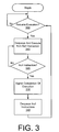
- FIG. 3 depicts an instruction execution operation of an embodiment of the memory controller 140 .
- the execution logic 195 of the memory controller 140 may determine whether to resume execution of the instructions in the memory controller pipeline 190 .
- the execution logic 195 determines to resume execution in response to the processor 100 asserting the dequeue signal DQP. Accordingly, the execution logic 195 may wait in block 300 until the processor 100 asserts the dequeue signal DQP.
- the execution logic 195 in block 310 may dequeue and execute an instruction of the memory controller pipeline 190 .
- the execution logic 195 may determine whether the next instruction (e.g. the instruction following the instruction dequeued and executed in block 310 ) of the memory controller pipeline 170 is a null instruction. If the instruction is not a null instruction, then the execution logic 195 returns to block 310 in order to dequeue and execute the instruction. In this manner, the execution logic 195 continues to execute instructions of the memory controller pipeline 170 until a null instruction is executed.
- the execution logic 195 in block 340 may signal completion of instructions associated with the received asserted dequeue signal DQP. In one embodiment, the execution logic 195 signals completion by deasserting the dequeue signal DQP. The execution logic 195 then in block 350 dequeues one or more null instructions NI of the memory controller pipeline 190 . In one embodiment, the execution logic 195 continues to dequeue instructions until a non-null instruction is encountered. In this manner, the execution logic 195 ensures that the memory controller pipeline 190 includes a non-null instruction to execute in response to the processor 100 requesting the memory controller 140 to resume execution.
- FIG. 4 depicts an instruction execution operation of an embodiment of the processor 100 .
- the processor may dequeue and execute an instruction of the processor pipeline 170 .
- the processor 100 may determine whether the next instruction (e.g. the instruction following the instruction dequeued and executed in block 410 ) of the processor pipeline 170 is a filler instruction FI. If the instruction is not a filler instruction FI, then the processor 100 may return to block 410 in order to dequeue and execute the instruction. In this manner, the processor 100 continues to execute instructions of the processor pipeline 170 until a filler instruction FI is encountered.
- the processor 100 may determine whether the memory controller 140 has completed the previous request for execution. In one embodiment, the processor 100 may determine that the memory controller 140 has completed the previous request in response to the memory controller 140 deasserting the dequeue signal DQP. If the previous request has not completed, then the processor 100 may wait in block 420 until the previous request has completed. In this manner, the processor 100 may execute instructions in parallel with instructions executed by the memory controller 140 after requesting the memory controller 140 to resume execution, but may maintain synchronization with the memory controller 140 by ensuring only one request for execution is pending at a time.
- the processor 100 in block 440 may signal that the memory controller 140 is to resume execution of the instructions in the memory controller pipeline 190 .
- the processor 100 may signal the resumption of the memory controller 140 by asserting the dequeue signal DQP.
- the processor 100 then in block 450 may dequeue one or more filler instructions FI of the processor pipeline 170 .
- the processor 100 may continue to dequeue instructions until a non-filler instruction is encountered. In this manner, the processor 100 may ensure that the memory controller pipeline 190 is signaled only once per a series of consecutive filler instructions FI in the processor pipeline 170 .
Abstract
Description
Claims (31)
Applications Claiming Priority (2)
| Application Number | Priority Date | Filing Date | Title |
|---|---|---|---|
| IN3469/DEL/2005 | 2005-12-23 | ||
| IN3469DE2005 | 2005-12-23 |
Publications (2)
| Publication Number | Publication Date |
|---|---|
| US20070150673A1 US20070150673A1 (en) | 2007-06-28 |
| US8190830B2 true US8190830B2 (en) | 2012-05-29 |
Family
ID=38195276
Family Applications (1)
| Application Number | Title | Priority Date | Filing Date |
|---|---|---|---|
| US11/372,647 Active 2030-04-14 US8190830B2 (en) | 2005-12-23 | 2006-03-10 | Method, apparatus, and systems to support execution pipelining in a memory controller |
Country Status (1)
| Country | Link |
|---|---|
| US (1) | US8190830B2 (en) |
Families Citing this family (4)
| Publication number | Priority date | Publication date | Assignee | Title |
|---|---|---|---|---|
| US8190830B2 (en) * | 2005-12-23 | 2012-05-29 | Intel Corporation | Method, apparatus, and systems to support execution pipelining in a memory controller |
| JP5292706B2 (en) * | 2007-02-28 | 2013-09-18 | 富士通セミコンダクター株式会社 | Computer system |
| US10496461B2 (en) * | 2011-06-15 | 2019-12-03 | Arm Finance Overseas Limited | Apparatus and method for hardware initiation of emulated instructions |
| US20230221958A1 (en) * | 2021-12-23 | 2023-07-13 | Intel Corporation | Memory controller with arithmetic logic unit and/or floating point unit |
Citations (7)
| Publication number | Priority date | Publication date | Assignee | Title |
|---|---|---|---|---|
| US3418638A (en) * | 1966-09-21 | 1968-12-24 | Ibm | Instruction processing unit for program branches |
| US3566366A (en) * | 1968-10-25 | 1971-02-23 | Bell Telephone Labor Inc | Selective execution circuit for program controlled data processors |
| US5434986A (en) * | 1992-01-09 | 1995-07-18 | Unisys Corporation | Interdependency control of pipelined instruction processor using comparing result of two index registers of skip instruction and next sequential instruction |
| US5664194A (en) * | 1995-12-04 | 1997-09-02 | Metricom, Inc. | Method for autonomously transferring code to a computer without accessing local memory by the central processing unit |
| US5922070A (en) * | 1994-01-11 | 1999-07-13 | Texas Instruments Incorporated | Pipelined data processing including program counter recycling |
| US20030088740A1 (en) * | 2001-10-23 | 2003-05-08 | Ip-First, Llc. | Microprocessor and method for performing selective prefetch based on bus activity level |
| US20070150673A1 (en) * | 2005-12-23 | 2007-06-28 | Rajaram G | Method, apparatus, and systems to support execution pipelining in a memory controller |
-
2006
- 2006-03-10 US US11/372,647 patent/US8190830B2/en active Active
Patent Citations (8)
| Publication number | Priority date | Publication date | Assignee | Title |
|---|---|---|---|---|
| US3418638A (en) * | 1966-09-21 | 1968-12-24 | Ibm | Instruction processing unit for program branches |
| US3566366A (en) * | 1968-10-25 | 1971-02-23 | Bell Telephone Labor Inc | Selective execution circuit for program controlled data processors |
| US5434986A (en) * | 1992-01-09 | 1995-07-18 | Unisys Corporation | Interdependency control of pipelined instruction processor using comparing result of two index registers of skip instruction and next sequential instruction |
| US5922070A (en) * | 1994-01-11 | 1999-07-13 | Texas Instruments Incorporated | Pipelined data processing including program counter recycling |
| US5664194A (en) * | 1995-12-04 | 1997-09-02 | Metricom, Inc. | Method for autonomously transferring code to a computer without accessing local memory by the central processing unit |
| US20030088740A1 (en) * | 2001-10-23 | 2003-05-08 | Ip-First, Llc. | Microprocessor and method for performing selective prefetch based on bus activity level |
| US6810466B2 (en) * | 2001-10-23 | 2004-10-26 | Ip-First, Llc | Microprocessor and method for performing selective prefetch based on bus activity level |
| US20070150673A1 (en) * | 2005-12-23 | 2007-06-28 | Rajaram G | Method, apparatus, and systems to support execution pipelining in a memory controller |
Non-Patent Citations (2)
| Title |
|---|
| Carter et al Impulse: Building a Smarter Memory Controller; In Proceedings of the 5th Int'l Symposium on High Performance Computer Architecture, pp. 70-79, Jan. 1999. |
| Zhang, et al: The Impulse Memory Controller; School of Computing, University of Utah, Sep. 24, 2001, 35 pages; IEEE Transactions on Computers, 50(11): p. 1117-1132, Nov. 2001. |
Also Published As
| Publication number | Publication date |
|---|---|
| US20070150673A1 (en) | 2007-06-28 |
Similar Documents
| Publication | Publication Date | Title |
|---|---|---|
| KR101746018B1 (en) | Method and apparatus for efficient scheduling for asymmetrical execution units | |
| KR101508566B1 (en) | Execute at commit state update instructions, apparatus, methods, and systems | |
| JP5963282B2 (en) | Interrupt distribution scheme | |
| US10241797B2 (en) | Replay reduction by wakeup suppression using early miss indication | |
| US20070162648A1 (en) | DMA Controller With Self-Detection For Global Clock-Gating Control | |
| US20080168191A1 (en) | Barrier and Interrupt Mechanism for High Latency and Out of Order DMA Device | |
| US20070204138A1 (en) | Device, system and method of tracking data validity | |
| US20080082755A1 (en) | Administering An Access Conflict In A Computer Memory Cache | |
| US8635477B2 (en) | Energy-efficient polling loop | |
| US20070038829A1 (en) | Wait aware memory arbiter | |
| WO2003058436A1 (en) | Instruction scheduling based on power estimation | |
| US6889279B2 (en) | Pre-stored vector interrupt handling system and method | |
| WO2013090425A1 (en) | A method, apparatus, and system for energy efficiency and energy conservation including code recirculation techniques | |
| KR101806279B1 (en) | Instruction order enforcement pairs of instructions, processors, methods, and systems | |
| WO2017172240A1 (en) | Processors, methods, systems, and instructions to fetch data to indicated cache level with guaranteed completion | |
| US20200301709A1 (en) | Processor with variable pre-fetch threshold | |
| US8190830B2 (en) | Method, apparatus, and systems to support execution pipelining in a memory controller | |
| US10210131B2 (en) | Synchronous data input/output system using prefetched device table entry | |
| US7966477B1 (en) | Power optimized replay of blocked operations in a pipilined architecture | |
| JP4817660B2 (en) | Apparatus and method for data bus output control | |
| US11467838B2 (en) | Fastpath microcode sequencer | |
| US9418024B2 (en) | Apparatus and method for efficient handling of critical chunks | |
| US20060218334A1 (en) | System and method to reduce memory latency in microprocessor systems connected with a bus | |
| US9552313B2 (en) | Delivering real time interrupts with an advanced programmable interrupt controller | |
| JP6227151B2 (en) | A scalable mechanism for executing monitoring instructions for writing to addresses |
Legal Events
| Date | Code | Title | Description |
|---|---|---|---|
| AS | Assignment |
Owner name: INTEL CORPORATION, CALIFORNIA Free format text: ASSIGNMENT OF ASSIGNORS INTEREST;ASSIGNOR:RAJARAM, G;REEL/FRAME:020131/0184 Effective date: 20060303 |
|
| FEPP | Fee payment procedure |
Free format text: PAYOR NUMBER ASSIGNED (ORIGINAL EVENT CODE: ASPN); ENTITY STATUS OF PATENT OWNER: LARGE ENTITY Free format text: PAYER NUMBER DE-ASSIGNED (ORIGINAL EVENT CODE: RMPN); ENTITY STATUS OF PATENT OWNER: LARGE ENTITY |
|
| STCF | Information on status: patent grant |
Free format text: PATENTED CASE |
|
| CC | Certificate of correction | ||
| FPAY | Fee payment |
Year of fee payment: 4 |
|
| MAFP | Maintenance fee payment |
Free format text: PAYMENT OF MAINTENANCE FEE, 8TH YEAR, LARGE ENTITY (ORIGINAL EVENT CODE: M1552); ENTITY STATUS OF PATENT OWNER: LARGE ENTITY Year of fee payment: 8 |
|
| MAFP | Maintenance fee payment |
Free format text: PAYMENT OF MAINTENANCE FEE, 12TH YEAR, LARGE ENTITY (ORIGINAL EVENT CODE: M1553); ENTITY STATUS OF PATENT OWNER: LARGE ENTITY Year of fee payment: 12 |