US8310384B2 - Phase digitizing apparatus and method thereof - Google Patents
Phase digitizing apparatus and method thereof Download PDFInfo
- Publication number
- US8310384B2 US8310384B2 US12/956,071 US95607110A US8310384B2 US 8310384 B2 US8310384 B2 US 8310384B2 US 95607110 A US95607110 A US 95607110A US 8310384 B2 US8310384 B2 US 8310384B2
- Authority
- US
- United States
- Prior art keywords
- phase
- code
- coarse
- phase code
- fine
- Prior art date
- Legal status (The legal status is an assumption and is not a legal conclusion. Google has not performed a legal analysis and makes no representation as to the accuracy of the status listed.)
- Active, expires
Links
Images


Classifications
-
- H—ELECTRICITY
- H03—ELECTRONIC CIRCUITRY
- H03M—CODING; DECODING; CODE CONVERSION IN GENERAL
- H03M1/00—Analogue/digital conversion; Digital/analogue conversion
- H03M1/12—Analogue/digital converters
Definitions
- the present invention relates to a phase digitizing apparatus and method thereof, and more particularly to a phase digitizing apparatus and method thereof for digitizing a phase of an input signal.
- a frequency synthesizer is an electronic system for generating a desired time domain signal, which can be found in many modern devices, including radio receivers, mobile telephones, radiotelephones, walkie-talkies, CB radios, satellite receivers, GPS systems, etc.
- the frequency synthesizer can combine frequency multiplication, frequency division, and frequency mixing (the frequency mixing process generates sum and difference frequencies) operations to produce the desired time domain signal.
- Synthesizers used in commercial radio receivers are largely based on phase-locked loops (PLLs). Many types of frequency synthesizers are available as integrated circuits, reducing cost and size. High end receivers and electronic test equipment use more sophisticated techniques, often in combination.
- PLLs phase-locked loops
- the frequency synthesizer comprises a phase error digitizer to calculate a phase error.
- FIG. 1 is a block diagram of a conventional phase error digitizer 10 .
- the conventional phase error digitizer 10 comprises a phase comparator 120 and a type converter 140 .
- the phase comparator 120 compares phases of two input signals, Hsync and FBsync, and outputs a comparison output CMPOut with only one bit.
- the difference in phase between the two input signals is called phase error.
- the type converter 140 converts the comparison output CMPOut with 1 bit to a phase error with 7 bits.
- phase error digitizer is difficult to design and implement, more expensive, larger and more sensitive to voltage noise, temperature and process than an all-digital phase error digitizer. Therefore, an all-digital phase error digitizer is urgently needed.
- the invention provides a phase digitizing apparatus for generating a corresponding digital value in response to a phase of an input signal, and comprises: a coarse phase generator, for generating a coarse phase code according to the phase of the input signal and a first time unit; a fine phase generator, for generating a fine phase code according to the phase of the input signal and a second time unit; and a calculating unit, for generating the digital value according to the coarse phase code and the fine phase code; wherein the first time unit is greater than the second time unit.
- the invention further provides a phase digitizing method for generating a corresponding digital value in response to a phase of an input signal, wherein the method comprises: generating a coarse phase code according to the phase of the input signal and a first time unit; generating a fine phase code according to the phase of the input signal and a second time unit; and generating the digital value according to the coarse phase code and the fine phase code; wherein the first time unit is greater than the second time unit.
- the invention provides a phase digitizing apparatus and method thereof including all digital circuits to address the disadvantages of a conventional phase error digitizing apparatus noted above.
- FIG. 1 is a block diagram of a conventional phase error digitizer
- FIG. 2 is a block diagram of a phase digitizing apparatus according to a first embodiment of the present invention
- FIG. 3 is a block diagram of an embodiment of a coarse phase code generator
- FIG. 4 illustrates a diagram for generating a coarse phase code and a fine phase code according to one embodiment of the present invention
- FIG. 5 illustrates a diagram for digitizing the phase according to one embodiment of the present invention
- FIG. 6 is a block diagram of the phase digitizing apparatus according to another embodiment of the invention.
- FIG. 7 illustrates a diagram for calibrating the phase according to one embodiment of the present invention
- FIG. 8 is a block diagram of the phase error digitizing apparatus according to one embodiment of the present invention.
- FIG. 9 illustrates a diagram for digitizing the phase error according to one embodiment of the invention.
- FIG. 10 is a flowchart of a phase digitizing method according to one embodiment of the invention.
- FIG. 2 is a block diagram of a phase digitizing apparatus according to a first embodiment of the present invention.
- the phase digitizing apparatus 20 comprises a coarse phase code generator 210 , a fine phase code generator 220 and a calculating unit 270 .
- the coarse phase code generator 210 generates a coarse phase code Cc according to a phase of an input signal In.
- the coarse phase code is a binary code that can be represented by binary 0 and 1.
- the fine phase code generator 220 generates a fine phase code Cf according to the phase of the input signal In.
- the coarse phase code generator 210 and the fine phase code generator 220 generate the coarse phase code Cc and the fine phase code Cf according to different time units respectively.
- the calculating unit 270 generates a phase digital value representing the phase of the input signal In according to the coarse phase code Cc and the fine phase code Cf.
- the phase is digitized to the coarse phase code Cc and the fine phase code Cf such that the phase is presented in a plurality of orders rather than in one single order.
- the final phase code is decided in multiple orders.
- the original phase code is 249
- the coarse time unit Tc of the coarse phase code Cc comprises 8 fine time units of the fine phase code Cf
- fewer clock signals are needed with different phases when presenting the phase code with multiple orders. Hence, it saves more dimensions and costs to use multiple orders of phase code.
- the coarse phase code generator 210 comprises a Gray code generator 212 and a phase code converter 214 .
- the input signal In passes the Gray code generator 212 to generate a Gray code corresponding to the phase of the input signal In.
- the Gray code is converted to the coarse phase code Cc by the phase code converter 214 . Since only one of the bits is different between two adjacent Gray codes, the Gray code substitutes the binary code to reduce interference of synchronization errors of the clock signal with pulse-code modulation (PCM).
- PCM pulse-code modulation
- FIG. 4 illustrates a diagram for generating the coarse phase code and the fine phase code according to one embodiment of the present invention.
- the coarse time unit and the fine time unit are generated according to the clock signal of a voltage-controlled oscillator (VCO).
- VCO voltage-controlled oscillator
- One clock period of the VCO is denoted as 1T.
- one clock period of the VCO corresponds to 2 coarse time units Tc
- one coarse time unit Tc corresponds to 4 fine phase time units Tf, i.e., one clock period of the VCO corresponds to 8 fine time units Tf.
- a coarse ruler Rc is generated according to the Gray code, and the coarse ruler Rc may be cyclic.
- the predetermined time is 4T, so the Gray code can be the same at every 4T distance.
- the coarse ruler Rc starts from 000, then 001, 011, 010, 110, 111, 101 and 100 takes place in turn, where the corresponding binary codes are 000 (0), 001 (1), 010 (2), 011 (3), 100 (4), 101 (5), 110 (6) and 111 (7), respectively.
- the coarse ruler Rc is cyclically back to 000.
- Gray code coding can be utilized, and one can customize the Gray code according to user's preference or requirement.
- the coarse ruler Rc can also be generated directly by a binary code. That is, the specific coding method of the coarse ruler should not be construed to limit the scope of the invention.
- the clock signal of the VCO is delayed one fine time unit Tf sequentially to generate a plurality of clock signals with different phases.
- one time length is divided into multiple fine time units Tf, and the fine time units are encoded sequentially to generate a fine ruler Rf shown in FIG. 4 .
- the clock signal of the VCO is delayed T/8 time units sequentially to generate 8 clock signals FCLK[1] ⁇ [8], where the two adjacent clock signals have one fine time unit Tf shift, and the corresponding fine ruler Rf is numbered from 1 to 8.
- the coarse phase code generator 210 and the fine phase code generator 220 decide the corresponding coarse phase code Cc and fine phase code Cf by detecting a positive edge triggered time point of the input signal In.
- the coarse phase code generator 210 detects the positive edge of the input signal In
- the coarse phase code Cc is generated according to the coarse ruler Rc.
- the fine phase code generator 220 detects the positive edge of the input signal In
- the fine phase code Cf is generated according to the clock signals FCLK[1] ⁇ [8]. For example, according to the positive edge of the input signal In, based on the levels of the clock signals FCLK[1] ⁇ [8], the corresponding value of each clock signal is decided sequentially.
- the fine phase code Cf of the positive edge of the input signal In is decided by each of the corresponding values of FCLK[1] ⁇ [8].
- the phase of the input signal In can also be detected by negative edge triggered detection.
- a line L represents the positive edge triggered time point of the input signal In.
- the Gray code generated by the Gray code generator 212 according to the coarse ruler Rc and the phase of the input signal In is ‘110’, which is 4 in decimal.
- the phase code converter 214 converts the Gary code 110 to binary code 110, that is, the coarse phase code Cc outputted from the coarse phase code generator 210 is ‘100’.
- the coarse phase code can be represented with other kinds of carry systems, and representation of the coarse phase code, as discussed, should not limit the scope of the invention.
- the fine phase code generator 220 detects the positive edge of the input signal In, based on the levels of the clock signals FCLK[1] ⁇ [8], the corresponding value is generated sequentially as [1 1 0 0 0 0 1 1]. Then, the boundary that 1 changes to 0 (zero) is determined at a point of 2 of the fine ruler Rf. That is to say, the fine phase code generator 220 outputs 2 as the fine phase code Cf which can also be represented as the binary code 010.
- FIG. 5 illustrates a diagram for digitizing the phase according to one embodiment of the present invention.
- one coarse time unit Tc comprises 8 fine time units Tf.
- FIG. 6 is a block diagram of the phase digitizing apparatus according to another embodiment of the invention.
- the phase digitizing apparatus 60 comprises a coarse phase code generator 630 , a fine phase code generator 640 , a phase calibration unit 660 and a calculating unit 680 .
- the coarse phase code generator 630 , the fine phase code generator 640 and the calculating unit 680 are similar to the above coarse phase code generator 210 , the fine phase code generator 220 and the calculating unit 270 respectively, and shall not be again described for brevity.
- the generating method can be realized by the embodiment illustrated in FIG. 4 and the clock signal for generating fine time unit Tf can be the same as the clock signal for generating coarse time unit Tc. Otherwise, the coarse time unit Tc and the fine time unit Tf can be generated according to different clock signals respectively. Consequently, due to errors caused by different clock signals or signal delay from circuits, misalignment exists between the starting point of the coarse time unit Tc and the starting point of the fine time unit Tf, that is, a phase error exists.
- the calculating unit 680 miscalculates the phase digital value because of the phase errors of the coarse time unit Tc and the fine time unit Tf.
- the phase calibration unit 660 calibrates the coarse phase code Cc and the fine phase code Cf by calibrating the phase error of the coarse phase code Cc and the fine phase code Cf caused by the difference of the starting point of the coarse time unit Tc and the starting point of the fine time unit Tf.
- the calibrating unit 680 can acquire more accurate phase digital value.
- the detail operation of the phase calibration unit 660 is described below.
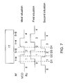
- FIG. 7 illustrates a diagram for calibrating the phase according to one embodiment of the present invention.
- the phase calibration unit 660 can calibrate the coarse phase code Cc according to the fine phase code Cf. It is noted that the phase calibration unit 660 can also calibrate the fine phase code Cf according to the coarse phase code Cc.
- the top row shows an ideal situation where the starting point of the coarse time unit Tc and the starting point of the fine time unit Tf are aligned.
- the second row shows a first situation in which the starting point of the coarse time unit Tc is later or behind the starting point of the fine time unit Tf.
- the bottom row shows a second situation in which the starting point of the coarse time unit Tc is ahead of or earlier than the starting point of the fine time unit Tf.
- the above situation can be detected by the following method:
- the coarse phase code should be odd. Supposing the coarse phase code is even, the starting point of the coarse time unit Tc is later than the starting point of the fine time unit Tf where the first dotted line D 1 is shown in FIG. 7 . Meanwhile, the coarse phase code is added by 1 for calibrating the phase code.
- the coarse phase code should be odd. Supposing the coarse phase code is even, the starting point of the coarse time unit Tc is earlier than the starting point of the fine time unit Tf where the second dotted line D 2 locates in FIG. 7 . Meanwhile, the coarse phase code is subtracted by 1 for calibrating the phase code.
- the coarse phase code should be even. Supposing the coarse phase code is odd, the starting point of the coarse time unit Tc is later than the starting point of the fine time unit Tf where the third dotted line D 3 is shown in FIG. 7 . Meanwhile, the coarse phase code is added by 1 for calibrating the phase code.
- the coarse phase code should be even. Supposing the coarse phase code is odd, the starting point of the coarse time unit Tc is ahead of the starting point of the fine time unit Tf, as shown by the fourth dotted line D 4 in FIG. 7 . Meanwhile, the coarse phase code is subtracted by 1 for calibrating the phase code.
- the above determining method is based on an error between the starting point of the coarse time unit Tc and the starting point of the fine time unit Tf that does not exceed 2 coarse time units Tc.
- this assumption does not hold, other calibration methods for calibrating the coarse phase code Cc and the fine phase code Cf can also be applied.
- FIG. 8 is a block diagram of the phase error digitizing apparatus according to one embodiment of the present invention.
- the phase error digitizing apparatus 80 comprises phase digitizing apparatuses 802 and 804 , and a phase error calculating unit 890 .
- the phase digitizing apparatuses 802 and 804 can be realized by the previous phase digitizing apparatuses 20 or 60 .
- the phase error digitizing apparatus 80 obtains phase digital values of input signals In 1 and In 2 by the phase digitizing apparatuses 802 and 804 respectively according to phases of the input signals In 1 and In 2 , and then the phase error calculating unit 890 calculates the difference between the phase digital values of the input signals In 1 and In 2 to generate the phase error.
- FIG. 9 illustrates a diagram for digitizing the phase error according to one embodiment of the invention. Operation details of the phase digitizing apparatuses 802 and 804 are similar to those in the foregoing description, and in FIG. 9 , differences are that one coarse time unit Tc comprises 9 fine time units Tf, the coarse ruler Rc is numbered from 0 to 63, and the fine ruler Rf is numbered from 0 to 17. In an embodiment, as a line L 11 shown in FIG.
- the situation with the smaller phase error can be selected.
- the phase error when the phase of the input signal In 2 is behind the phase of the input signal In 1 , the phase error is 332; however, when the phase of the input signal In 2 is ahead of the phase of the input signal In 1 , the phase error is 244, and since 244 is smaller than 332, the situation with the smaller phase error 244 is selected. That is, the phase of the input signal In 2 is ahead of the phase of the input signal In 1 , and the phase error is 244 fine time units Tf. It is noted that when the VCO is very inaccurate, the situation with the larger phase error can also be selected.
- FIG. 10 is a flowchart of a phase digitizing method according to one embodiment of the invention.
- Step 1020 comprises generating a coarse phase code according to a phase of an input signal and a coarse time unit Tc.
- the coarse time unit Tc generates a coarse ruler Rc numbered by the Gray code sequentially within a predetermined time, i.e., values of the Gray code with a time shift of a multiple of the predetermined time are the same.
- the coarse ruler Rc starts from 000, and 001, 011, 010, 110, 111, 101 and 100 in turn, after 4T time, the coarse ruler Rc is cyclically back to 000, and the corresponding binary codes are 000 (0), 001 (1), 010 (2), 011 (3), 100 (4), 101 (5), 110 (6) and 111 (7), respectively.
- the phase is detected as shown at a line L.
- the Gray code is 110, i.e., 4, and then the Gray code 110 is converted to the binary code 100, i.e., the coarse phase code Cc is 100.
- Step 1040 comprises generating a fine phase code according to the phase of the input signal and a fine time unit Tf.
- the phase is detected as shown at the line L.
- the corresponding value is generated sequentially as [1 1 0 0 0 0 1 1].
- the boundary that 1 changes to 0 is determined at 2 of the fine ruler Rf. That is to say, the fine phase code Cf is 2, which can also be represented as the binary code 010.
- the phase digitizing apparatus of the invention can be applied on any systems or circuits needing phase error calculation, such as a phase-locked loop (PLL) or a frequency synthesizer.
- a phase-locked loop PLL
- a frequency synthesizer When an apparatus, such as the PLL, calculates the phase error according to the invention, considering the system stability and preventing the misjudgment from a burst error, it is preferred not to adjust the phase much at once. Accordingly, an upper bound of the phase error can be set. When the phase error is greater than the upper bound, the phase error is set to be the upper bound. In a preferable embodiment, the upper bound can be set to 35 fine time units Tf, i.e., not beyond 1T.
- phase errors are both greater than the upper bound 35, so the final outputting phase errors can be set to 35.
- the original phase error can also be outputted, and the latter apparatus can be used to determine whether the phase error exceeds the upper bound.
Abstract
Description
7Tc*8Tf/Tc+2Tf=58Tf (fine time units)
22Tc*9Tf/Tc+6Tf=204Tf (fine time units)
38Tc*9Tf/Tc+5Tf=347Tf (fine time units)
14Tc*9Tf/Tc+3Tf=129Tf (fine time units)
51Tc*9Tf/Tc+2Tf=461Tf (fine time units)
7Tc*8Tf/Tc+2Tf=58Tf (fine time units)
Claims (18)
Priority Applications (1)
| Application Number | Priority Date | Filing Date | Title |
|---|---|---|---|
| US12/956,071 US8310384B2 (en) | 2010-02-03 | 2010-11-30 | Phase digitizing apparatus and method thereof |
Applications Claiming Priority (2)
| Application Number | Priority Date | Filing Date | Title |
|---|---|---|---|
| US30083110P | 2010-02-03 | 2010-02-03 | |
| US12/956,071 US8310384B2 (en) | 2010-02-03 | 2010-11-30 | Phase digitizing apparatus and method thereof |
Publications (2)
| Publication Number | Publication Date |
|---|---|
| US20110187567A1 US20110187567A1 (en) | 2011-08-04 |
| US8310384B2 true US8310384B2 (en) | 2012-11-13 |
Family
ID=44341143
Family Applications (1)
| Application Number | Title | Priority Date | Filing Date |
|---|---|---|---|
| US12/956,071 Active 2031-02-11 US8310384B2 (en) | 2010-02-03 | 2010-11-30 | Phase digitizing apparatus and method thereof |
Country Status (3)
| Country | Link |
|---|---|
| US (1) | US8310384B2 (en) |
| CN (1) | CN102142835B (en) |
| TW (1) | TWI429203B (en) |
Cited By (3)
| Publication number | Priority date | Publication date | Assignee | Title |
|---|---|---|---|---|
| US20150071396A1 (en) * | 2013-09-11 | 2015-03-12 | Fujitsu Semiconductor Limited | Method for determining phase of clock used for reception of parallel data, receiving circuit, and electronic apparatus |
| US10225070B2 (en) * | 2016-04-14 | 2019-03-05 | Ibiquity Digital Corporation | Time-alignment measurment for hybrid HD radio technology |
| US10666416B2 (en) | 2016-04-14 | 2020-05-26 | Ibiquity Digital Corporation | Time-alignment measurement for hybrid HD radio technology |
Citations (4)
| Publication number | Priority date | Publication date | Assignee | Title |
|---|---|---|---|---|
| US6125158A (en) * | 1997-12-23 | 2000-09-26 | Nortel Networks Corporation | Phase locked loop and multi-stage phase comparator |
| US6912012B2 (en) * | 2001-07-20 | 2005-06-28 | Texas Instruments Incorporated | Video decoder having lock algorithm that distinguishes between a noisy television signal input and a video recorder signal |
| US7339408B2 (en) * | 2003-12-12 | 2008-03-04 | Micron Technology | Generating multi-phase clock signals using hierarchical delays |
| US7734002B2 (en) * | 2006-11-14 | 2010-06-08 | Integrated Device Technology, Inc. | Phase difference detector having concurrent fine and coarse capabilities |
Family Cites Families (2)
| Publication number | Priority date | Publication date | Assignee | Title |
|---|---|---|---|---|
| DE19941445A1 (en) * | 1999-08-30 | 2001-03-01 | Thomson Brandt Gmbh | Phase detector for a phase locked loop |
| CN1393992A (en) * | 2001-07-02 | 2003-01-29 | 朗迅科技公司 | Delay compensating circuit containing feedback loop |
-
2010
- 2010-05-28 TW TW099117304A patent/TWI429203B/en not_active IP Right Cessation
- 2010-06-03 CN CN2010102005001A patent/CN102142835B/en active Active
- 2010-11-30 US US12/956,071 patent/US8310384B2/en active Active
Patent Citations (4)
| Publication number | Priority date | Publication date | Assignee | Title |
|---|---|---|---|---|
| US6125158A (en) * | 1997-12-23 | 2000-09-26 | Nortel Networks Corporation | Phase locked loop and multi-stage phase comparator |
| US6912012B2 (en) * | 2001-07-20 | 2005-06-28 | Texas Instruments Incorporated | Video decoder having lock algorithm that distinguishes between a noisy television signal input and a video recorder signal |
| US7339408B2 (en) * | 2003-12-12 | 2008-03-04 | Micron Technology | Generating multi-phase clock signals using hierarchical delays |
| US7734002B2 (en) * | 2006-11-14 | 2010-06-08 | Integrated Device Technology, Inc. | Phase difference detector having concurrent fine and coarse capabilities |
Cited By (6)
| Publication number | Priority date | Publication date | Assignee | Title |
|---|---|---|---|---|
| US20150071396A1 (en) * | 2013-09-11 | 2015-03-12 | Fujitsu Semiconductor Limited | Method for determining phase of clock used for reception of parallel data, receiving circuit, and electronic apparatus |
| US9124416B2 (en) * | 2013-09-11 | 2015-09-01 | Socionext Inc. | Method for determining phase of clock used for reception of parallel data, receiving circuit, and electronic apparatus |
| US10225070B2 (en) * | 2016-04-14 | 2019-03-05 | Ibiquity Digital Corporation | Time-alignment measurment for hybrid HD radio technology |
| US10666416B2 (en) | 2016-04-14 | 2020-05-26 | Ibiquity Digital Corporation | Time-alignment measurement for hybrid HD radio technology |
| US11190334B2 (en) | 2016-04-14 | 2021-11-30 | Ibiquity Digital Corporation | Time-alignment measurement for hybrid HD radio™ technology |
| USRE48966E1 (en) | 2016-04-14 | 2022-03-08 | Ibiquity Digital Corporation | Time-alignment measurement for hybrid HD radio™ technology |
Also Published As
| Publication number | Publication date |
|---|---|
| CN102142835B (en) | 2013-01-09 |
| TW201128960A (en) | 2011-08-16 |
| CN102142835A (en) | 2011-08-03 |
| TWI429203B (en) | 2014-03-01 |
| US20110187567A1 (en) | 2011-08-04 |
Similar Documents
| Publication | Publication Date | Title |
|---|---|---|
| US8571161B2 (en) | Electronic device for generating a fractional frequency | |
| KR100500925B1 (en) | Low jitter dll using 2 coarse half delay line with digital phase mixer | |
| JP5347534B2 (en) | Phase comparator, PLL circuit, and phase comparator control method | |
| KR101632657B1 (en) | Time-to-digital convertoer and all-digital phase locked loop | |
| US8390347B1 (en) | Single period phase to digital converter | |
| JP4648380B2 (en) | Fractional frequency synthesizer | |
| US8536911B1 (en) | PLL circuit, method of controlling PLL circuit, and digital circuit | |
| US20070291173A1 (en) | Phase lock loop and digital control oscillator thereof | |
| US8575980B2 (en) | PLL circuit, error correcting method for the same, and communication apparatus including the same | |
| US8237511B2 (en) | Local oscillator and phase adjusting method for the same | |
| US10164622B2 (en) | Circuit and method for reducing mismatch for combined clock signal | |
| US9698807B1 (en) | Time signal conversion using dual time-based digital-to-analog converters | |
| US8310384B2 (en) | Phase digitizing apparatus and method thereof | |
| US8325870B2 (en) | Digital phase-locked loops and frequency adjusting methods thereof | |
| US10826507B1 (en) | Fractional divider with error correction | |
| US6838912B1 (en) | Digital fractional phase detector | |
| US9461811B1 (en) | Clock and data recovery circuit and clock and data recovery method | |
| WO2009083501A2 (en) | A phase locked loop | |
| US20190207612A1 (en) | Digital downconverter with digital oscillator frequency error correction | |
| US8451965B2 (en) | Semiconductor integrated circuit, radio communication device and time to digital converter | |
| Huang et al. | A time-to-digital converter based AFC for wideband frequency synthesizer | |
| US11509314B2 (en) | All-digital phase-locked loop | |
| US11588490B2 (en) | Digital loop filter in all-digital phase-locked loop | |
| US8872559B2 (en) | Numerically controlled oscillator and digital phase-locked loop | |
| JP4956989B2 (en) | Clock synchronization method and clock synchronization circuit |
Legal Events
| Date | Code | Title | Description |
|---|---|---|---|
| AS | Assignment |
Owner name: MSTAR SEMICONDUCTOR, INC., TAIWAN Free format text: ASSIGNMENT OF ASSIGNORS INTEREST;ASSIGNORS:YEH, PO LIN;LIN, CHIEN-HSING;HUNG, SHAO PING;AND OTHERS;SIGNING DATES FROM 20100715 TO 20100910;REEL/FRAME:025432/0505 |
|
| STCF | Information on status: patent grant |
Free format text: PATENTED CASE |
|
| FPAY | Fee payment |
Year of fee payment: 4 |
|
| AS | Assignment |
Owner name: MEDIATEK INC., TAIWAN Free format text: MERGER;ASSIGNOR:MSTAR SEMICONDUCTOR, INC.;REEL/FRAME:050665/0001 Effective date: 20190124 |
|
| MAFP | Maintenance fee payment |
Free format text: PAYMENT OF MAINTENANCE FEE, 8TH YEAR, LARGE ENTITY (ORIGINAL EVENT CODE: M1552); ENTITY STATUS OF PATENT OWNER: LARGE ENTITY Year of fee payment: 8 |
|
| AS | Assignment |
Owner name: XUESHAN TECHNOLOGIES INC., CANADA Free format text: ASSIGNMENT OF ASSIGNORS INTEREST;ASSIGNOR:MEDIATEK INC.;REEL/FRAME:055486/0870 Effective date: 20201223 |