US8711309B2 - Liquid crystal display having wide viewing angle - Google Patents
Liquid crystal display having wide viewing angle Download PDFInfo
- Publication number
- US8711309B2 US8711309B2 US13/774,095 US201313774095A US8711309B2 US 8711309 B2 US8711309 B2 US 8711309B2 US 201313774095 A US201313774095 A US 201313774095A US 8711309 B2 US8711309 B2 US 8711309B2
- Authority
- US
- United States
- Prior art keywords
- liquid crystal
- crystal display
- group
- aperture
- domains
- Prior art date
- Legal status (The legal status is an assumption and is not a legal conclusion. Google has not performed a legal analysis and makes no representation as to the accuracy of the status listed.)
- Expired - Fee Related
Links
Images


Classifications
-
- G—PHYSICS
- G02—OPTICS
- G02F—OPTICAL DEVICES OR ARRANGEMENTS FOR THE CONTROL OF LIGHT BY MODIFICATION OF THE OPTICAL PROPERTIES OF THE MEDIA OF THE ELEMENTS INVOLVED THEREIN; NON-LINEAR OPTICS; FREQUENCY-CHANGING OF LIGHT; OPTICAL LOGIC ELEMENTS; OPTICAL ANALOGUE/DIGITAL CONVERTERS
- G02F1/00—Devices or arrangements for the control of the intensity, colour, phase, polarisation or direction of light arriving from an independent light source, e.g. switching, gating or modulating; Non-linear optics
- G02F1/01—Devices or arrangements for the control of the intensity, colour, phase, polarisation or direction of light arriving from an independent light source, e.g. switching, gating or modulating; Non-linear optics for the control of the intensity, phase, polarisation or colour
- G02F1/13—Devices or arrangements for the control of the intensity, colour, phase, polarisation or direction of light arriving from an independent light source, e.g. switching, gating or modulating; Non-linear optics for the control of the intensity, phase, polarisation or colour based on liquid crystals, e.g. single liquid crystal display cells
- G02F1/133—Constructional arrangements; Operation of liquid crystal cells; Circuit arrangements
- G02F1/1333—Constructional arrangements; Manufacturing methods
- G02F1/1337—Surface-induced orientation of the liquid crystal molecules, e.g. by alignment layers
- G02F1/133753—Surface-induced orientation of the liquid crystal molecules, e.g. by alignment layers with different alignment orientations or pretilt angles on a same surface, e.g. for grey scale or improved viewing angle
-
- G—PHYSICS
- G02—OPTICS
- G02F—OPTICAL DEVICES OR ARRANGEMENTS FOR THE CONTROL OF LIGHT BY MODIFICATION OF THE OPTICAL PROPERTIES OF THE MEDIA OF THE ELEMENTS INVOLVED THEREIN; NON-LINEAR OPTICS; FREQUENCY-CHANGING OF LIGHT; OPTICAL LOGIC ELEMENTS; OPTICAL ANALOGUE/DIGITAL CONVERTERS
- G02F1/00—Devices or arrangements for the control of the intensity, colour, phase, polarisation or direction of light arriving from an independent light source, e.g. switching, gating or modulating; Non-linear optics
- G02F1/01—Devices or arrangements for the control of the intensity, colour, phase, polarisation or direction of light arriving from an independent light source, e.g. switching, gating or modulating; Non-linear optics for the control of the intensity, phase, polarisation or colour
- G02F1/13—Devices or arrangements for the control of the intensity, colour, phase, polarisation or direction of light arriving from an independent light source, e.g. switching, gating or modulating; Non-linear optics for the control of the intensity, phase, polarisation or colour based on liquid crystals, e.g. single liquid crystal display cells
- G02F1/133—Constructional arrangements; Operation of liquid crystal cells; Circuit arrangements
- G02F1/1333—Constructional arrangements; Manufacturing methods
- G02F1/1337—Surface-induced orientation of the liquid crystal molecules, e.g. by alignment layers
- G02F1/133707—Structures for producing distorted electric fields, e.g. bumps, protrusions, recesses, slits in pixel electrodes
-
- G—PHYSICS
- G02—OPTICS
- G02F—OPTICAL DEVICES OR ARRANGEMENTS FOR THE CONTROL OF LIGHT BY MODIFICATION OF THE OPTICAL PROPERTIES OF THE MEDIA OF THE ELEMENTS INVOLVED THEREIN; NON-LINEAR OPTICS; FREQUENCY-CHANGING OF LIGHT; OPTICAL LOGIC ELEMENTS; OPTICAL ANALOGUE/DIGITAL CONVERTERS
- G02F1/00—Devices or arrangements for the control of the intensity, colour, phase, polarisation or direction of light arriving from an independent light source, e.g. switching, gating or modulating; Non-linear optics
- G02F1/01—Devices or arrangements for the control of the intensity, colour, phase, polarisation or direction of light arriving from an independent light source, e.g. switching, gating or modulating; Non-linear optics for the control of the intensity, phase, polarisation or colour
- G02F1/13—Devices or arrangements for the control of the intensity, colour, phase, polarisation or direction of light arriving from an independent light source, e.g. switching, gating or modulating; Non-linear optics for the control of the intensity, phase, polarisation or colour based on liquid crystals, e.g. single liquid crystal display cells
- G02F1/133—Constructional arrangements; Operation of liquid crystal cells; Circuit arrangements
- G02F1/1333—Constructional arrangements; Manufacturing methods
- G02F1/1343—Electrodes
-
- G—PHYSICS
- G02—OPTICS
- G02F—OPTICAL DEVICES OR ARRANGEMENTS FOR THE CONTROL OF LIGHT BY MODIFICATION OF THE OPTICAL PROPERTIES OF THE MEDIA OF THE ELEMENTS INVOLVED THEREIN; NON-LINEAR OPTICS; FREQUENCY-CHANGING OF LIGHT; OPTICAL LOGIC ELEMENTS; OPTICAL ANALOGUE/DIGITAL CONVERTERS
- G02F1/00—Devices or arrangements for the control of the intensity, colour, phase, polarisation or direction of light arriving from an independent light source, e.g. switching, gating or modulating; Non-linear optics
- G02F1/01—Devices or arrangements for the control of the intensity, colour, phase, polarisation or direction of light arriving from an independent light source, e.g. switching, gating or modulating; Non-linear optics for the control of the intensity, phase, polarisation or colour
- G02F1/13—Devices or arrangements for the control of the intensity, colour, phase, polarisation or direction of light arriving from an independent light source, e.g. switching, gating or modulating; Non-linear optics for the control of the intensity, phase, polarisation or colour based on liquid crystals, e.g. single liquid crystal display cells
- G02F1/133—Constructional arrangements; Operation of liquid crystal cells; Circuit arrangements
- G02F1/1333—Constructional arrangements; Manufacturing methods
- G02F1/1335—Structural association of cells with optical devices, e.g. polarisers or reflectors
- G02F1/133528—Polarisers
-
- G—PHYSICS
- G02—OPTICS
- G02F—OPTICAL DEVICES OR ARRANGEMENTS FOR THE CONTROL OF LIGHT BY MODIFICATION OF THE OPTICAL PROPERTIES OF THE MEDIA OF THE ELEMENTS INVOLVED THEREIN; NON-LINEAR OPTICS; FREQUENCY-CHANGING OF LIGHT; OPTICAL LOGIC ELEMENTS; OPTICAL ANALOGUE/DIGITAL CONVERTERS
- G02F1/00—Devices or arrangements for the control of the intensity, colour, phase, polarisation or direction of light arriving from an independent light source, e.g. switching, gating or modulating; Non-linear optics
- G02F1/01—Devices or arrangements for the control of the intensity, colour, phase, polarisation or direction of light arriving from an independent light source, e.g. switching, gating or modulating; Non-linear optics for the control of the intensity, phase, polarisation or colour
- G02F1/13—Devices or arrangements for the control of the intensity, colour, phase, polarisation or direction of light arriving from an independent light source, e.g. switching, gating or modulating; Non-linear optics for the control of the intensity, phase, polarisation or colour based on liquid crystals, e.g. single liquid crystal display cells
- G02F1/133—Constructional arrangements; Operation of liquid crystal cells; Circuit arrangements
- G02F1/1333—Constructional arrangements; Manufacturing methods
- G02F1/1337—Surface-induced orientation of the liquid crystal molecules, e.g. by alignment layers
-
- G—PHYSICS
- G02—OPTICS
- G02F—OPTICAL DEVICES OR ARRANGEMENTS FOR THE CONTROL OF LIGHT BY MODIFICATION OF THE OPTICAL PROPERTIES OF THE MEDIA OF THE ELEMENTS INVOLVED THEREIN; NON-LINEAR OPTICS; FREQUENCY-CHANGING OF LIGHT; OPTICAL LOGIC ELEMENTS; OPTICAL ANALOGUE/DIGITAL CONVERTERS
- G02F1/00—Devices or arrangements for the control of the intensity, colour, phase, polarisation or direction of light arriving from an independent light source, e.g. switching, gating or modulating; Non-linear optics
- G02F1/01—Devices or arrangements for the control of the intensity, colour, phase, polarisation or direction of light arriving from an independent light source, e.g. switching, gating or modulating; Non-linear optics for the control of the intensity, phase, polarisation or colour
- G02F1/13—Devices or arrangements for the control of the intensity, colour, phase, polarisation or direction of light arriving from an independent light source, e.g. switching, gating or modulating; Non-linear optics for the control of the intensity, phase, polarisation or colour based on liquid crystals, e.g. single liquid crystal display cells
- G02F1/133—Constructional arrangements; Operation of liquid crystal cells; Circuit arrangements
- G02F1/1333—Constructional arrangements; Manufacturing methods
- G02F1/1343—Electrodes
- G02F1/134309—Electrodes characterised by their geometrical arrangement
- G02F1/134336—Matrix
-
- G—PHYSICS
- G02—OPTICS
- G02F—OPTICAL DEVICES OR ARRANGEMENTS FOR THE CONTROL OF LIGHT BY MODIFICATION OF THE OPTICAL PROPERTIES OF THE MEDIA OF THE ELEMENTS INVOLVED THEREIN; NON-LINEAR OPTICS; FREQUENCY-CHANGING OF LIGHT; OPTICAL LOGIC ELEMENTS; OPTICAL ANALOGUE/DIGITAL CONVERTERS
- G02F1/00—Devices or arrangements for the control of the intensity, colour, phase, polarisation or direction of light arriving from an independent light source, e.g. switching, gating or modulating; Non-linear optics
- G02F1/01—Devices or arrangements for the control of the intensity, colour, phase, polarisation or direction of light arriving from an independent light source, e.g. switching, gating or modulating; Non-linear optics for the control of the intensity, phase, polarisation or colour
- G02F1/13—Devices or arrangements for the control of the intensity, colour, phase, polarisation or direction of light arriving from an independent light source, e.g. switching, gating or modulating; Non-linear optics for the control of the intensity, phase, polarisation or colour based on liquid crystals, e.g. single liquid crystal display cells
- G02F1/133—Constructional arrangements; Operation of liquid crystal cells; Circuit arrangements
- G02F1/1333—Constructional arrangements; Manufacturing methods
- G02F1/1343—Electrodes
- G02F1/13439—Electrodes characterised by their electrical, optical, physical properties; materials therefor; method of making
-
- G—PHYSICS
- G02—OPTICS
- G02F—OPTICAL DEVICES OR ARRANGEMENTS FOR THE CONTROL OF LIGHT BY MODIFICATION OF THE OPTICAL PROPERTIES OF THE MEDIA OF THE ELEMENTS INVOLVED THEREIN; NON-LINEAR OPTICS; FREQUENCY-CHANGING OF LIGHT; OPTICAL LOGIC ELEMENTS; OPTICAL ANALOGUE/DIGITAL CONVERTERS
- G02F1/00—Devices or arrangements for the control of the intensity, colour, phase, polarisation or direction of light arriving from an independent light source, e.g. switching, gating or modulating; Non-linear optics
- G02F1/01—Devices or arrangements for the control of the intensity, colour, phase, polarisation or direction of light arriving from an independent light source, e.g. switching, gating or modulating; Non-linear optics for the control of the intensity, phase, polarisation or colour
- G02F1/13—Devices or arrangements for the control of the intensity, colour, phase, polarisation or direction of light arriving from an independent light source, e.g. switching, gating or modulating; Non-linear optics for the control of the intensity, phase, polarisation or colour based on liquid crystals, e.g. single liquid crystal display cells
- G02F1/133—Constructional arrangements; Operation of liquid crystal cells; Circuit arrangements
- G02F1/1333—Constructional arrangements; Manufacturing methods
- G02F1/1335—Structural association of cells with optical devices, e.g. polarisers or reflectors
- G02F1/13363—Birefringent elements, e.g. for optical compensation
- G02F1/133634—Birefringent elements, e.g. for optical compensation the refractive index Nz perpendicular to the element surface being different from in-plane refractive indices Nx and Ny, e.g. biaxial or with normal optical axis
-
- G—PHYSICS
- G02—OPTICS
- G02F—OPTICAL DEVICES OR ARRANGEMENTS FOR THE CONTROL OF LIGHT BY MODIFICATION OF THE OPTICAL PROPERTIES OF THE MEDIA OF THE ELEMENTS INVOLVED THEREIN; NON-LINEAR OPTICS; FREQUENCY-CHANGING OF LIGHT; OPTICAL LOGIC ELEMENTS; OPTICAL ANALOGUE/DIGITAL CONVERTERS
- G02F1/00—Devices or arrangements for the control of the intensity, colour, phase, polarisation or direction of light arriving from an independent light source, e.g. switching, gating or modulating; Non-linear optics
- G02F1/01—Devices or arrangements for the control of the intensity, colour, phase, polarisation or direction of light arriving from an independent light source, e.g. switching, gating or modulating; Non-linear optics for the control of the intensity, phase, polarisation or colour
- G02F1/13—Devices or arrangements for the control of the intensity, colour, phase, polarisation or direction of light arriving from an independent light source, e.g. switching, gating or modulating; Non-linear optics for the control of the intensity, phase, polarisation or colour based on liquid crystals, e.g. single liquid crystal display cells
- G02F1/133—Constructional arrangements; Operation of liquid crystal cells; Circuit arrangements
- G02F1/1333—Constructional arrangements; Manufacturing methods
- G02F1/1337—Surface-induced orientation of the liquid crystal molecules, e.g. by alignment layers
- G02F1/133742—Surface-induced orientation of the liquid crystal molecules, e.g. by alignment layers for homeotropic alignment
-
- G—PHYSICS
- G02—OPTICS
- G02F—OPTICAL DEVICES OR ARRANGEMENTS FOR THE CONTROL OF LIGHT BY MODIFICATION OF THE OPTICAL PROPERTIES OF THE MEDIA OF THE ELEMENTS INVOLVED THEREIN; NON-LINEAR OPTICS; FREQUENCY-CHANGING OF LIGHT; OPTICAL LOGIC ELEMENTS; OPTICAL ANALOGUE/DIGITAL CONVERTERS
- G02F1/00—Devices or arrangements for the control of the intensity, colour, phase, polarisation or direction of light arriving from an independent light source, e.g. switching, gating or modulating; Non-linear optics
- G02F1/01—Devices or arrangements for the control of the intensity, colour, phase, polarisation or direction of light arriving from an independent light source, e.g. switching, gating or modulating; Non-linear optics for the control of the intensity, phase, polarisation or colour
- G02F1/13—Devices or arrangements for the control of the intensity, colour, phase, polarisation or direction of light arriving from an independent light source, e.g. switching, gating or modulating; Non-linear optics for the control of the intensity, phase, polarisation or colour based on liquid crystals, e.g. single liquid crystal display cells
- G02F1/133—Constructional arrangements; Operation of liquid crystal cells; Circuit arrangements
- G02F1/1333—Constructional arrangements; Manufacturing methods
- G02F1/1337—Surface-induced orientation of the liquid crystal molecules, e.g. by alignment layers
- G02F1/133753—Surface-induced orientation of the liquid crystal molecules, e.g. by alignment layers with different alignment orientations or pretilt angles on a same surface, e.g. for grey scale or improved viewing angle
- G02F1/133757—Surface-induced orientation of the liquid crystal molecules, e.g. by alignment layers with different alignment orientations or pretilt angles on a same surface, e.g. for grey scale or improved viewing angle with different alignment orientations
-
- G—PHYSICS
- G02—OPTICS
- G02F—OPTICAL DEVICES OR ARRANGEMENTS FOR THE CONTROL OF LIGHT BY MODIFICATION OF THE OPTICAL PROPERTIES OF THE MEDIA OF THE ELEMENTS INVOLVED THEREIN; NON-LINEAR OPTICS; FREQUENCY-CHANGING OF LIGHT; OPTICAL LOGIC ELEMENTS; OPTICAL ANALOGUE/DIGITAL CONVERTERS
- G02F1/00—Devices or arrangements for the control of the intensity, colour, phase, polarisation or direction of light arriving from an independent light source, e.g. switching, gating or modulating; Non-linear optics
- G02F1/01—Devices or arrangements for the control of the intensity, colour, phase, polarisation or direction of light arriving from an independent light source, e.g. switching, gating or modulating; Non-linear optics for the control of the intensity, phase, polarisation or colour
- G02F1/13—Devices or arrangements for the control of the intensity, colour, phase, polarisation or direction of light arriving from an independent light source, e.g. switching, gating or modulating; Non-linear optics for the control of the intensity, phase, polarisation or colour based on liquid crystals, e.g. single liquid crystal display cells
- G02F1/137—Devices or arrangements for the control of the intensity, colour, phase, polarisation or direction of light arriving from an independent light source, e.g. switching, gating or modulating; Non-linear optics for the control of the intensity, phase, polarisation or colour based on liquid crystals, e.g. single liquid crystal display cells characterised by the electro-optical or magneto-optical effect, e.g. field-induced phase transition, orientation effect, guest-host interaction or dynamic scattering
- G02F1/13712—Devices or arrangements for the control of the intensity, colour, phase, polarisation or direction of light arriving from an independent light source, e.g. switching, gating or modulating; Non-linear optics for the control of the intensity, phase, polarisation or colour based on liquid crystals, e.g. single liquid crystal display cells characterised by the electro-optical or magneto-optical effect, e.g. field-induced phase transition, orientation effect, guest-host interaction or dynamic scattering the liquid crystal having negative dielectric anisotropy
-
- G—PHYSICS
- G02—OPTICS
- G02F—OPTICAL DEVICES OR ARRANGEMENTS FOR THE CONTROL OF LIGHT BY MODIFICATION OF THE OPTICAL PROPERTIES OF THE MEDIA OF THE ELEMENTS INVOLVED THEREIN; NON-LINEAR OPTICS; FREQUENCY-CHANGING OF LIGHT; OPTICAL LOGIC ELEMENTS; OPTICAL ANALOGUE/DIGITAL CONVERTERS
- G02F1/00—Devices or arrangements for the control of the intensity, colour, phase, polarisation or direction of light arriving from an independent light source, e.g. switching, gating or modulating; Non-linear optics
- G02F1/01—Devices or arrangements for the control of the intensity, colour, phase, polarisation or direction of light arriving from an independent light source, e.g. switching, gating or modulating; Non-linear optics for the control of the intensity, phase, polarisation or colour
- G02F1/13—Devices or arrangements for the control of the intensity, colour, phase, polarisation or direction of light arriving from an independent light source, e.g. switching, gating or modulating; Non-linear optics for the control of the intensity, phase, polarisation or colour based on liquid crystals, e.g. single liquid crystal display cells
- G02F1/137—Devices or arrangements for the control of the intensity, colour, phase, polarisation or direction of light arriving from an independent light source, e.g. switching, gating or modulating; Non-linear optics for the control of the intensity, phase, polarisation or colour based on liquid crystals, e.g. single liquid crystal display cells characterised by the electro-optical or magneto-optical effect, e.g. field-induced phase transition, orientation effect, guest-host interaction or dynamic scattering
- G02F1/139—Devices or arrangements for the control of the intensity, colour, phase, polarisation or direction of light arriving from an independent light source, e.g. switching, gating or modulating; Non-linear optics for the control of the intensity, phase, polarisation or colour based on liquid crystals, e.g. single liquid crystal display cells characterised by the electro-optical or magneto-optical effect, e.g. field-induced phase transition, orientation effect, guest-host interaction or dynamic scattering based on orientation effects in which the liquid crystal remains transparent
- G02F1/1393—Devices or arrangements for the control of the intensity, colour, phase, polarisation or direction of light arriving from an independent light source, e.g. switching, gating or modulating; Non-linear optics for the control of the intensity, phase, polarisation or colour based on liquid crystals, e.g. single liquid crystal display cells characterised by the electro-optical or magneto-optical effect, e.g. field-induced phase transition, orientation effect, guest-host interaction or dynamic scattering based on orientation effects in which the liquid crystal remains transparent the birefringence of the liquid crystal being electrically controlled, e.g. ECB-, DAP-, HAN-, PI-LC cells
-
- G—PHYSICS
- G02—OPTICS
- G02F—OPTICAL DEVICES OR ARRANGEMENTS FOR THE CONTROL OF LIGHT BY MODIFICATION OF THE OPTICAL PROPERTIES OF THE MEDIA OF THE ELEMENTS INVOLVED THEREIN; NON-LINEAR OPTICS; FREQUENCY-CHANGING OF LIGHT; OPTICAL LOGIC ELEMENTS; OPTICAL ANALOGUE/DIGITAL CONVERTERS
- G02F1/00—Devices or arrangements for the control of the intensity, colour, phase, polarisation or direction of light arriving from an independent light source, e.g. switching, gating or modulating; Non-linear optics
- G02F1/01—Devices or arrangements for the control of the intensity, colour, phase, polarisation or direction of light arriving from an independent light source, e.g. switching, gating or modulating; Non-linear optics for the control of the intensity, phase, polarisation or colour
- G02F1/13—Devices or arrangements for the control of the intensity, colour, phase, polarisation or direction of light arriving from an independent light source, e.g. switching, gating or modulating; Non-linear optics for the control of the intensity, phase, polarisation or colour based on liquid crystals, e.g. single liquid crystal display cells
- G02F1/137—Devices or arrangements for the control of the intensity, colour, phase, polarisation or direction of light arriving from an independent light source, e.g. switching, gating or modulating; Non-linear optics for the control of the intensity, phase, polarisation or colour based on liquid crystals, e.g. single liquid crystal display cells characterised by the electro-optical or magneto-optical effect, e.g. field-induced phase transition, orientation effect, guest-host interaction or dynamic scattering
- G02F1/139—Devices or arrangements for the control of the intensity, colour, phase, polarisation or direction of light arriving from an independent light source, e.g. switching, gating or modulating; Non-linear optics for the control of the intensity, phase, polarisation or colour based on liquid crystals, e.g. single liquid crystal display cells characterised by the electro-optical or magneto-optical effect, e.g. field-induced phase transition, orientation effect, guest-host interaction or dynamic scattering based on orientation effects in which the liquid crystal remains transparent
- G02F1/1396—Devices or arrangements for the control of the intensity, colour, phase, polarisation or direction of light arriving from an independent light source, e.g. switching, gating or modulating; Non-linear optics for the control of the intensity, phase, polarisation or colour based on liquid crystals, e.g. single liquid crystal display cells characterised by the electro-optical or magneto-optical effect, e.g. field-induced phase transition, orientation effect, guest-host interaction or dynamic scattering based on orientation effects in which the liquid crystal remains transparent the liquid crystal being selectively controlled between a twisted state and a non-twisted state, e.g. TN-LC cell
-
- G—PHYSICS
- G02—OPTICS
- G02F—OPTICAL DEVICES OR ARRANGEMENTS FOR THE CONTROL OF LIGHT BY MODIFICATION OF THE OPTICAL PROPERTIES OF THE MEDIA OF THE ELEMENTS INVOLVED THEREIN; NON-LINEAR OPTICS; FREQUENCY-CHANGING OF LIGHT; OPTICAL LOGIC ELEMENTS; OPTICAL ANALOGUE/DIGITAL CONVERTERS
- G02F2201/00—Constructional arrangements not provided for in groups G02F1/00 - G02F7/00
- G02F2201/12—Constructional arrangements not provided for in groups G02F1/00 - G02F7/00 electrode
- G02F2201/121—Constructional arrangements not provided for in groups G02F1/00 - G02F7/00 electrode common or background
Definitions
- the present invention relates to a liquid crystal display having wide viewing angle.
- a liquid crystal display includes two substrates and a liquid crystal layer interposed therebetween.
- the transmittance of the incident light is controlled by the strength of the electric field applied to the liquid crystal layer.
- a vertically aligned twisted nematic (VATN) liquid crystal display has a couple of transparent substrates which have transparent electrodes on their inner surfaces and a couple of polarizers attached to their outer surfaces.
- the VATN LCD further includes a liquid crystal layer between the two substrates, and the liquid crystal layer has chirality and negative dielectric anisotropy.
- the long axes of the liquid crystal molecules are aligned perpendicular to the substrates.
- the VATN LCD having crossed polarizers may have sufficiently dark state. Therefore, the contrast ratio of the VATN LCD is relatively high compared with the conventional TN LCD. However, the viewing angle of the VATN LCD may not be so wide due to the difference in retardation values among viewing directions.
- the proposed structures may not have a sufficiently wide viewing angle and the luminance in their on states is not so high.
- a liquid crystal display includes a first and a second substrate facing each other and a first and a second electrodes on inner surfaces of the first and the second substrates respectively.
- the first and the second electrodes face each other, and have a plurality of first apertures and a plurality of second apertures, respectively.
- the first and the second apertures form a substantially closed area.
- the boundaries of the first and the second apertures are linear, curved or bent with an obtuse angle.
- the width of the first and the second apertures becomes larger as goes from the ends to the center.
- the width of the first and the second apertures are 3-20 ⁇ m.
- the distance between the first and the second apertures are 5-20 ⁇ m.
- the liquid crystal display according to the present invention may include a liquid crystal layer between the first and the second substrates, a first and a second alignment layers on the first and the second electrodes, respectively, and a first and a second polarizers attached on the outer surfaces of the first and the second substrates, respectively.
- the liquid crystal layer has negative dielectric anisotropy, and the first and the second alignment layer force the long axes of the liquid crystal molecules to align perpendicular to the first and the second substrates.
- the polarizing directions of the first and the second polarizers are preferably perpendicular to each other. It is preferable that the number of the average directions of the long axes of the liquid crystal molecules in the domains defined by the first and the second apertures are four. Preferably, the average directions makes 45° ⁇ 10° with the polarizing directions of the first and the second polarizers, and the average directions of the adjacent domains are substantially perpendicular to each other.
- the shape of the first and the second electrodes according to the present invention makes the liquid crystal layer therebetween to be divided into four regions having different average directions of the long axes, thereby causing wide viewing angle.
- disclination due to the disorder of the liquid crystal molecules is reduced by adjusting the widths and shapes of the apertures.
- FIGS. 1A and 1B are schematic diagrams of a VATN LCD according to an embodiment of the present invention, respectively in black state and white state.
- FIG. 2 is a schematic sectional view of a VATN LCD according an embodiment of the present invention
- FIG. 3 is a layout view of apertures in electrodes of a VATN LCD according to the first embodiment of the present invention.
- FIG. 4 is a sectional view of a liquid crystal display taken along the line IV-IV in FIG. 3 .
- FIG. 5 is a layout view of apertures in electrodes of a VATN LCD according to the second embodiment of the present invention.
- FIG. 6 is a layout view of apertures in electrodes of a VATN LCD according to the third embodiment of the present invention.
- FIG. 7 is a sectional view of a liquid crystal display taken along the line IV-IV in FIG. 6 .
- FIGS. 8 and 9 are layout views of apertures in electrodes of VATN LCDs according to the fourth and fifth embodiments of the present invention.
- FIG. 10 is a sectional view of a liquid crystal display according to an embodiment of the present invention.
- FIGS. 11 to 15 are layout views of apertures in electrodes of VATN LCDs according to the sixth to tenth embodiments of the present invention.
- FIGS. 1A and 1B are schematic diagrams of a VAIN LCD according to an embodiment of the present invention, respectively in black state and white state.
- two glass or quartz insulating substrates 10 and 20 faces each other with being spaced apart from each other.
- Field generating electrodes 11 and 21 made of a transparent conductive material such as ITO (indium tin oxide) or the like are formed on the inner surfaces of the substrates 10 and 20 , respectively, and homeotropic alignment layers 12 and 22 are formed thereon, respectively.
- a liquid crystal layer 100 including a nematic liquid crystal having negative dielectric anisotropy is interposed between the substrates 10 and 20 .
- the liquid crystal layer 100 may have chirality or the alignment layers 12 and 22 may be rubbed in some directions so that the director of the liquid crystal layer 100 twists from the one alignment layer to the other.
- Polarizers 13 and 23 are attached on the outer surfaces of the substrates 10 and 20 , respectively, and polarize the rays out of the liquid crystal layer 100 and the rays incident on the liquid crystal layer 100 , respectively.
- the polarizing directions of the polarizers 13 and 23 are perpendicular to each other.
- the alignment layers 12 and 22 may be rubbed or not.
- FIG. 1A shows the off state that there is no potential difference between the electrodes 11 and 21 .
- long axes or molecular axes of the liquid crystal molecules 110 in the liquid crystal layer 100 are aligned perpendicular to the surfaces of the substrates 10 and 20 due to the aligning force of the alignment layers 12 and 22 .
- the incident light linearly polarized by the polarizer 23 attached to the lower substrate 20 passes through the liquid crystal layer 100 without changing its polarization. Then, the light is blocked by the analyzer 13 attached to the upper substrate 10 to make the LCD in a black state.
- FIG. 1B shows the on state that the sufficient electric field due to the high potential difference between the electrodes 11 and 21 is applied to the liquid crystal layer 100 .
- the molecular axes of the liquid crystal molecules in the liquid crystal layer 100 becomes perpendicular to the field direction or parallel to the substrates 11 and 21 due to the dielectric anisotropy.
- the molecules 110 near the surface of the alignment layers 12 and 22 remains in its initial state since the aligning force by the alignment layers 12 and 22 is much larger than the force due to the dielectric anisotropy.
- the liquid crystal director twists spirally due to the chirality or rubbing. By adjusting the chirality of the liquid crystal layer 100 , the twist angle of the liquid crystal director from the lower substrate 10 to the upper substrate 20 may made to be 90°.
- the incident light linearly polarized by the polarizer 23 passes through the liquid crystal layer 100 and its polarization rotates by 90° according to the twist of the liquid crystal director. Therefore, the light passes through the analyzer 13 to make the LCD in a white state.
- FIG. 2 shows the schematic structure of a VATN LCD having apertures in electrodes according to an embodiment of the present invention. For convenience, only substrates and electrodes are depicted and the other elements such as alignment layers are abbreviated.
- field-generating electrodes 11 and 21 are formed on the upper and the lower substrates 10 and 20 , respectively, and the electrode 21 formed on the lower substrate 20 has an aperture 200 .
- the long axes of the liquid crystal molecules 110 are aligned perpendicular to the substrates 10 and 20 , as shown in FIG. 1A .
- the electrodes 11 and 21 have potential difference, an electric field is generated. Although the field direction in most regions is perpendicular to the substrates 10 and 20 , the field direction near the aperture 200 is not completely perpendicular to the substrates 10 and 20 , and the electric field is symmetrical with respect to the aperture 100 . The electric field near the aperture 200 is called the fringe field.
- the long axes of the liquid crystal molecules are not perpendicular to the substrates 10 and 20 and make some angle. The arrangement of the liquid crystal molecules are almost symmetrical with respect to the aperture 200 and the liquid crystal molecules in opposite regions with respect to the aperture 200 are arranged in opposite manner, thereby causing wide viewing angle.
- the strength of the fringe field is large near the aperture and becomes smaller as goes far from the aperture. Accordingly, if the distance between the apertures is properly adjusted, the liquid crystal molecules located between the apertures are sufficiently affected by the fringe field.
- the liquid crystal layer is divided into several regions or domains defined by the apertures, and the average axial direction, which means the average direction of the long axes of the liquid crystal molecules, in each domain is varied according to the shapes and arrangement of the apertures.
- the aperture 200 is formed when a conductive layer is patterned to form the electrode 21 by using photolithography, no separate step for forming the aperture 20 is required, and thus it is very easy to obtain a multi-domain LCD compared with other methods using such as rubbing.
- the locations and the shapes of the domains can be finely adjustable because of the use of the photolithgraphy.
- a plurality of wires (not shown) for supplying signals to the electrode 21 may be provided on the lower substrate 20 . In this case, portions of the electrode 11 on the upper substrate 10 located at the position corresponding to wires on the lower substrate 20 may be removed in order to reduce the parasitic capacitance between the electrode 11 and the wires.
- the apertures 200 may have various shapes and arrangements, and the apertures may be formed in both electrodes or either of the electrodes. Since the shapes and arrangements of the apertures affects on the average axial directions of the domains and characteristics such as luminance, response time and afterimages, etc., of the LCD panels, they should be properly designed.
- the aperture pattern for a multi-domain LCD according to the present invention satisfies the following conditions:
- the number of the domains which have different average axial directions, especially in a pixel is at least two, and more preferably the number is four.
- the average axial direction of each domain when viewed from the top, preferably makes 45° ⁇ 10°, more preferably 45° with the polarizing directions of the polarizers especially when using crossed polarizers.
- the average axial directions of the adjacent domains are perpendicular to each other.
- the apertures on the upper and the lower substrates form substantially closed areas and thus substantially closed domains, when viewed from the top. It is because that the texture where the arrangement of the liquid crystal molecules is disordered is generated near the ends of the apertures, and thus the ends of the apertures are preferably closely located. Furthermore, the boundaries of the apertures are preferably linear, slowly curved or bent with an obtuse angle in order to make the arrangement of the liquid crystal molecules to be uniform, thereby reducing the response time. In particular, when the apertures on the lower and upper substrates face each other and form a substantially closed area, it is preferable that the boundaries of the facing portions of the apertures are preferably linear, slowly curved or bent with an obtuse angle. It is preferable that the width of the aperture becomes larger as goes from the ends to the center.
- the aperture patterns may be rectangular.
- the width of the aperture and the distance between the apertures are preferably 3-20 ⁇ m and 5-20 ⁇ m. If the width of the aperture is larger than the former value or the distance between the apertures is less than the latter value, the aperture ratio is reduced, thereby reducing luminance and transmittance. On the contrary, if the width of the aperture is less than the former value or the distance between the apertures is larger than the latter value, the strength of the fringe field becomes week, thereby increasing response time and generating disordered textures.
- FIGS. 3 and 4 show a single pixel region 300 .
- FIGS. 3 and 4 show a single pixel region 300 .
- aperture patterns are illustrated in FIGS. 3 and 4 , and other elements such as TFTs, wires, etc., are not illustrated.
- a plurality of linear apertures 211 , 212 , 216 and 217 are formed in a rectangular pixel region 300 .
- a plurality of first and second apertures 211 and 212 extending in transverse and longitudinal directions respectively are formed in an electrode 11 on an upper substrate 10
- a cross-shaped aperture 216 and 217 including first and second portions 216 and 217 extending in the transverse and longitudinal directions respectively are formed in an electrode 21 on a lower substrate 20 .
- the first and the second apertures 211 and 212 are separated from each other, arranged in the longitudinal direction, and form four large squares which is substantially closed.
- the first portion 216 of the lower aperture passes through the center of the pixel 300 in the longitudinal direction, and thus through the center of the large squares formed by the first and the second apertures 211 and 212 , and both ends of the first portion 216 approaches the second apertures 212 .
- the plurality of second portions 217 passes through the center of the large squares in the transverse direction, and both ends of the second portion 216 approaches the first apertures 211 .
- the apertures 211 , 212 , 216 and 217 form small squares which define domains, and two edges of the small square is two apertures 211 and 212 on the upper substrate 10 , while the other two edges of the small square is two apertures 216 and 217 on the lower substrate 20 .
- the liquid crystal molecules incline due to the fringe field near the apertures.
- the adjacent apertures 211 and 216 on the different substrates 10 and 20 result in a fringe field which forces the liquid crystal molecules between the apertures 211 and 216 to align in the same direction, i.e., the direction from the aperture 216 to the aperture 211 . Accordingly, the tilt directions of the liquid crystal molecules in the opposing regions with respect to the apertures are different.
- the director of the liquid crystal layer varies in accordance with position.
- the average axial direction in a square domain becomes the direction from the intersection of the first and the second portions 216 and 217 to the intersection of the extensions of the first and the second apertures. That is, the average axial direction in a square domain is the direction from the center to the corner of the large square formed by the first and the second apertures 211 and 212 .
- This arrangement of the aperture makes sixteen square domains in a pixel, and the average axial direction of each domain is one of four directions. The average axial directions of the adjacent domains are perpendicular to each other when viewed from the top.
- the polarizing directions P 1 and P 2 of the polarizers When the polarizing directions P 1 and P 2 of the polarizers are aligned in the transverse and the longitudinal directions respectively, the polarizing directions P 1 and P 2 have an angle of 45° relative to the average axial direction of each domain when a sufficient voltage is applied.
- the liquid crystal molecules are rearranged by the force due to the electric field immediately after the voltage is applied.
- the arrangement of the liquid crystal molecules is slowly changed by the tendency to be parallel to each other, which the molecules of the nematic liquid crystal have. Accordingly, it takes some time to reach a stable state that the movement of the liquid crystal molecules disappears, thereby causing large response time.
- An aperture pattern according to the second embodiment of the present invention shown in FIG. 5 is similar to the aperture pattern shown in FIG. 3 except for rectangular shape of the domains instead of square shape. That is, longitudinal apertures 221 and 226 are longer than transverse apertures 222 and 227 . Accordingly, when viewed from the top, an angle made by the average axial directions in the adjacent domains is not exactly 90°, and an angle between the polarizing directions and the average axial directions is not exactly 45°. However, in this case, one of the transverse or longitudinal directions is preferred by the liquid crystal molecules because the long axes of the liquid crystal molecules makes a less angle with one of the two directions than with the other. Since the rearrangement of the liquid crystal molecules quickly occurred and becomes stable, the response time is relatively short than the LCD shown in FIG. 3 .
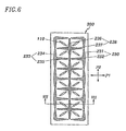
- FIG. 6 is a layout view of an aperture pattern of an LCD according to a third embodiment of the present invention
- FIG. 5 is a sectional view of the LCD shown in FIG. 6 taken along the line VII-VII′.
- an LCD according to the third embodiment of the present invention includes a lower TFT (thin film transistor) panel 20 and an upper color filter panel 10 .
- a plurality of gate lines and data lines are formed on the inner surface of the TFT panel 20 , and a pixel electrode 20 and a TFT (now shown) as a switching element are formed in a lower pixel region surrounded by the gate lines and data lines.
- a black matrix pattern 14 which defines an upper pixel region corresponding to the lower pixel region in the TFT panel is formed, and a color filter 15 is formed therebetween.
- a passivation layer 16 covers the black matrix 14 and the color filter 15 , and a common electrode 11 is formed thereon.
- a plurality of apertures 230 , 233 and 238 are formed in the common electrode 11 and the pixel electrode 21 , and homeotropic alignment layers 25 and 15 are formed on the pixel electrode 21 and the common electrode 11 , respectively.
- Polarizers 13 and 23 are attached to the outer surfaces of the substrates 10 and 20 , respectively, and retardation films 17 and 27 are interposed between the polarizers 13 and 23 and the substrates 10 and 20 , respectively.
- An a-plate compensation film and a c-plate compensation film may be attached to respective substrates, or two c-plate compensation films may be attached the both substrates 10 and 20 .
- a biaxial compensation film may be used instead of the uniaxial compensation film, and, in this case, the biaxial compensation film may be attached to only one substrate.
- the slow axis, which is the direction having a largest refractive index, of the a-plate or biaxial compensation film may be parallel or perpendicular to the polarizing directions. It is preferable that the second slow axis of the biaxial compensation film coincides the transmission or absorption axes of the polarizers.
- the shapes of the apertures 230 , 233 and 238 are basically similar to those of the LCD shown in FIG. 3 according to the first embodiment.
- the apertures 230 and 233 on the color filter panel 10 includes longitudinal parts 231 and 234 and transverse parts 232 and 235 extending from the center of the longitudinal parts 231 and 233 in the left or right direction.
- the apertures 233 and 230 located near the left and right edges of the pixel is symmetrically arranged with respect to the longitudinal central line of the pixel, and form four large rectangles (almost squares) arranged in the longitudinal direction.
- the plurality of the apertures 238 on the TFT panel 20 have cross shapes including transverse parts 237 and longitudinal parts 236 crossing each other, and the centers of the apertures 238 are located at the center of the large rectangles.
- the ends of the apertures 230 , 233 and 238 on the substrates 10 and 20 are as close as possible such that the domain defined by the apertures 230 , 233 and 238 form a substantially closed area when viewed from the top.
- the width of the apertures 230 , 233 and 238 is largest at the center, and decreases as goes to the ends. Therefore, the boundaries of the apertures 230 , 233 and 238 are bent with obtuse angle, and the angle made by two apertures on the different substrates are acute angle when viewed from the top.
- the domain defined by the apertures 13 and 23 has the diagonal substantially perpendicular to the average axial direction which is longer than the diagonal substantially parallel to the average axial direction.
- the ratio of the diagonal perpendicular to the average axial direction with respect to the diagonal parallel to the average axial direction becomes larger if the width difference between the central portion and the end portion of the apertures 230 , 233 and 238 is more enlarged at the bent point. Since the liquid crystal molecules become more uniformly aligned as the apertures 13 and 23 are parallel to each other, the response time becomes reduced as the ratio becomes large.
- the average axial directions of the adjacent domains makes 90 degrees
- the polarizing directions P 1 and P 2 of the polarizers 13 and 23 are perpendicular to each other and makes 45 degrees with the average axial direction of each domain.
- the apertures preferably form regular tetragonal rings.
- the width of the apertures 230 , 233 and 238 is preferably in the range of 3-20 ⁇ m as described above.
- the distance between the central points of the apertures 230 , 233 and 238 on the different substrates 10 and 20 which is largest distance between the apertures, is in the range of 10-50 ⁇ m and more preferably in the range of 23-30 ⁇ m. However, it depends on the size or the shape of the pixel.
- FIG. 8 a fourth embodiment of the present invention is described with reference to FIG. 8 .
- the shape of apertures is similar to that of the third embodiment.
- the boundaries of the apertures 230 , 233 and 238 are bent twice while those in the third embodiment once, when only a domain is considered.
- the edges 241 and 242 generated by the twice bending of the boundaries of the apertures 230 , 233 and 238 on the different substrates 10 and 20 are parallel to each other.
- the central portions of the apertures 230 , 233 and 238 expand to the center of the domain, the central portions 239 of the apertures 238 becomes square.
- the distance between the apertures 230 , 233 and 238 becomes much smaller, and the boundaries of the apertures 230 , 233 and 238 approaches linear shape, thereby decreasing response time.
- the aperture ratio decreases since the area occupied by the apertures 233 , 233 and 238 becomes larger, the aperture ratio decreases.
- the central portion 239 of the aperture 238 on the lower substrate 20 in the fourth embodiment becomes square ring instead of square in the fifth embodiment.
- the cross shaped aperture 238 is divided two portions 245 and 246 in order to prevent the isolation of the portion of the electrode surrounded by the central portion of the aperture 238 . That is, two adjacent edges of the square ring is connected to each other, but disconnected to the remaining two edges. Furthermore, an aperture 247 parallel to the opposing edges of the square ring is added. As a result, two domains are added in the square ring, and the aperture ratio increases.
- aperture ratio and luminance may be improved if edge portions of the apertures 230 and 233 on the upper substrate 10 are placed outside the pixel electrode 21 as shown in FIG. 10 .
- the shapes of the apertures on the two substrates may be exchanged.
- the apertures on the different substrates are parallel to each other, which is the sixth embodiment shown in FIG. 11 .
- a linear aperture 252 extending longitudinally is formed in the center of a pixel electrode on a TFT panel 20 , and two linear longitudinal apertures 251 on a color filter panel 10 are located left and right to the aperture 252 , and thus the apertures on the different substrates are arranged alternately.
- Polarizing directions P 1 and P 2 are perpendicular to each other and make an angle of 45° with respect to the extension of the apertures 251 and 252 .
- the response time is very fast as about 30 ms.
- the viewing angle is not good compared with the former embodiments.
- FIG. 12 Another aperture pattern for obtaining fast response time as well as four average axial directions is provided in the seventh embodiment of the present invention shown in FIG. 12 .
- FIG. 12 shows two adjacent pixels 310 and 320 and an aperture pattern formed thereon.
- Apertures 253 and 255 on the upper substrate 10 and apertures 254 and 256 extend obliquely to make an angle with the transverse and the longitudinal directions.
- the apertures 253 , 254 , 255 and 256 in a pixel 310 and 320 are parallel to each other, and the extensions of the apertures in the adjacent pixels makes an angle such as 90 degrees. In this case, a pair of pixels yields 4 different average axial directions.
- Polarizing directions P 1 and P 2 are aligned in the transverse and longitudinal directions.
- the disclination that the liquid crystal molecules are disordered may be generated near the intersections of the pixel electrodes and the apertures 254 and 256 on the lower substrate 20 , more exactly, at the portion where the apertures makes an obtuse angle with the pixel electrode.
- the disclination reduces the luminance of the LCD, and afterimage may be generated since the position of the disclination region varies according to the applied voltage.
- FIG. 13 which illustrate the eighth embodiment of the present invention, shows a branch 257 of the aperture 253 on the color filter substrate, which extends to the point where the boundary of the pixel electrode 21 and the aperture 253 make an obtuse angle along the edges of the pixel electrode 21 .
- the width of the branch 257 may gradually decrease from the connection with the apertures 253 to the ends. This shape decreases the disclination and increases the luminance.
- two average axial directions exist in a pixel, and four average axial directions. In a pair of the pixel regions.
- FIGS. 14 and 15 The various arrangement of pixels having different average axial directions are possible, and these embodiments are shown in FIGS. 14 and 15 .
- the pixels arranged in the row direction has the same average axial direction, while the adjacent pixels in a column have different average axial directions.
- the oblique angles of apertures is differentiated.
- the oblique angles of the apertures of adjacent pixels in a column are different, while, in row direction, the pixels in a dot including red, green and blue pixels has the same average axial direction, and the average axial direction is altered by unit of dot.
- multi-domain LCDs are formed using various aperture pattern to control the arrangement of liquid crystal molecules, therefore wide viewing angle is obtained, disclination is removed and the luminance is increased.
Abstract
Description
Claims (57)
Priority Applications (3)
| Application Number | Priority Date | Filing Date | Title |
|---|---|---|---|
| US13/774,095 US8711309B2 (en) | 1998-05-19 | 2013-02-22 | Liquid crystal display having wide viewing angle |
| US14/202,483 US20140184995A1 (en) | 1998-05-19 | 2014-03-10 | Liquid crystal display having wide viewing angle |
| US15/095,513 US9977289B2 (en) | 1998-05-19 | 2016-04-11 | Liquid crystal display having wide viewing angle |
Applications Claiming Priority (12)
| Application Number | Priority Date | Filing Date | Title |
|---|---|---|---|
| KR10-1998-0018037 | 1998-05-19 | ||
| KR1019980018037A KR100354904B1 (en) | 1998-05-19 | 1998-05-19 | Liquid crystal display with wide viewing angle |
| US09/314,293 US6342938B1 (en) | 1998-05-19 | 1999-05-19 | Liquid crystal display having electrodes with apertures wherein the apertures have different shapes |
| US10/020,303 US6512568B2 (en) | 1998-05-19 | 2001-12-18 | Liquid crystal display having wide viewing angle |
| US10/269,861 US6778244B2 (en) | 1998-05-19 | 2002-10-15 | Liquid crystal display having wide viewing angle |
| US10/861,397 US6937311B2 (en) | 1998-05-19 | 2004-06-07 | Liquid crystal display having domain dividers |
| US11/183,744 US7050134B2 (en) | 1998-05-19 | 2005-07-19 | Tilted multi domain liquid crystal display |
| US11/398,839 US7787086B2 (en) | 1998-05-19 | 2006-04-06 | Liquid crystal display having wide viewing angle |
| US12/147,697 US7787087B2 (en) | 1998-05-19 | 2008-06-27 | Liquid crystal display having wide viewing angle |
| US12/840,634 US8054430B2 (en) | 1998-05-19 | 2010-07-21 | Liquid crystal display having wide viewing angle |
| US13/241,327 US8400598B2 (en) | 1998-05-19 | 2011-09-23 | Liquid crystal display having wide viewing angle |
| US13/774,095 US8711309B2 (en) | 1998-05-19 | 2013-02-22 | Liquid crystal display having wide viewing angle |
Related Parent Applications (1)
| Application Number | Title | Priority Date | Filing Date |
|---|---|---|---|
| US13/241,327 Continuation US8400598B2 (en) | 1998-05-19 | 2011-09-23 | Liquid crystal display having wide viewing angle |
Related Child Applications (1)
| Application Number | Title | Priority Date | Filing Date |
|---|---|---|---|
| US14/202,483 Continuation US20140184995A1 (en) | 1998-05-19 | 2014-03-10 | Liquid crystal display having wide viewing angle |
Publications (2)
| Publication Number | Publication Date |
|---|---|
| US20130201433A1 US20130201433A1 (en) | 2013-08-08 |
| US8711309B2 true US8711309B2 (en) | 2014-04-29 |
Family
ID=19537498
Family Applications (12)
| Application Number | Title | Priority Date | Filing Date |
|---|---|---|---|
| US09/314,293 Expired - Lifetime US6342938B1 (en) | 1998-05-19 | 1999-05-19 | Liquid crystal display having electrodes with apertures wherein the apertures have different shapes |
| US10/020,303 Expired - Lifetime US6512568B2 (en) | 1998-05-19 | 2001-12-18 | Liquid crystal display having wide viewing angle |
| US10/269,861 Expired - Lifetime US6778244B2 (en) | 1998-05-19 | 2002-10-15 | Liquid crystal display having wide viewing angle |
| US10/861,397 Expired - Lifetime US6937311B2 (en) | 1998-05-19 | 2004-06-07 | Liquid crystal display having domain dividers |
| US11/183,744 Expired - Lifetime US7050134B2 (en) | 1998-05-19 | 2005-07-19 | Tilted multi domain liquid crystal display |
| US11/398,839 Expired - Fee Related US7787086B2 (en) | 1998-05-19 | 2006-04-06 | Liquid crystal display having wide viewing angle |
| US12/147,697 Expired - Fee Related US7787087B2 (en) | 1998-05-19 | 2008-06-27 | Liquid crystal display having wide viewing angle |
| US12/840,634 Expired - Fee Related US8054430B2 (en) | 1998-05-19 | 2010-07-21 | Liquid crystal display having wide viewing angle |
| US13/241,327 Expired - Fee Related US8400598B2 (en) | 1998-05-19 | 2011-09-23 | Liquid crystal display having wide viewing angle |
| US13/774,095 Expired - Fee Related US8711309B2 (en) | 1998-05-19 | 2013-02-22 | Liquid crystal display having wide viewing angle |
| US14/202,483 Abandoned US20140184995A1 (en) | 1998-05-19 | 2014-03-10 | Liquid crystal display having wide viewing angle |
| US15/095,513 Expired - Fee Related US9977289B2 (en) | 1998-05-19 | 2016-04-11 | Liquid crystal display having wide viewing angle |
Family Applications Before (9)
| Application Number | Title | Priority Date | Filing Date |
|---|---|---|---|
| US09/314,293 Expired - Lifetime US6342938B1 (en) | 1998-05-19 | 1999-05-19 | Liquid crystal display having electrodes with apertures wherein the apertures have different shapes |
| US10/020,303 Expired - Lifetime US6512568B2 (en) | 1998-05-19 | 2001-12-18 | Liquid crystal display having wide viewing angle |
| US10/269,861 Expired - Lifetime US6778244B2 (en) | 1998-05-19 | 2002-10-15 | Liquid crystal display having wide viewing angle |
| US10/861,397 Expired - Lifetime US6937311B2 (en) | 1998-05-19 | 2004-06-07 | Liquid crystal display having domain dividers |
| US11/183,744 Expired - Lifetime US7050134B2 (en) | 1998-05-19 | 2005-07-19 | Tilted multi domain liquid crystal display |
| US11/398,839 Expired - Fee Related US7787086B2 (en) | 1998-05-19 | 2006-04-06 | Liquid crystal display having wide viewing angle |
| US12/147,697 Expired - Fee Related US7787087B2 (en) | 1998-05-19 | 2008-06-27 | Liquid crystal display having wide viewing angle |
| US12/840,634 Expired - Fee Related US8054430B2 (en) | 1998-05-19 | 2010-07-21 | Liquid crystal display having wide viewing angle |
| US13/241,327 Expired - Fee Related US8400598B2 (en) | 1998-05-19 | 2011-09-23 | Liquid crystal display having wide viewing angle |
Family Applications After (2)
| Application Number | Title | Priority Date | Filing Date |
|---|---|---|---|
| US14/202,483 Abandoned US20140184995A1 (en) | 1998-05-19 | 2014-03-10 | Liquid crystal display having wide viewing angle |
| US15/095,513 Expired - Fee Related US9977289B2 (en) | 1998-05-19 | 2016-04-11 | Liquid crystal display having wide viewing angle |
Country Status (4)
| Country | Link |
|---|---|
| US (12) | US6342938B1 (en) |
| JP (2) | JP4714315B2 (en) |
| KR (1) | KR100354904B1 (en) |
| TW (1) | TW408247B (en) |
Cited By (1)
| Publication number | Priority date | Publication date | Assignee | Title |
|---|---|---|---|---|
| US20160223871A1 (en) * | 1998-05-19 | 2016-08-04 | Samsung Display Co., Ltd. | Liquid crystal display having wide viewing angle |
Families Citing this family (144)
| Publication number | Priority date | Publication date | Assignee | Title |
|---|---|---|---|---|
| JP3398025B2 (en) * | 1997-10-01 | 2003-04-21 | 三洋電機株式会社 | Liquid crystal display |
| US7663607B2 (en) | 2004-05-06 | 2010-02-16 | Apple Inc. | Multipoint touchscreen |
| KR100309918B1 (en) * | 1998-05-16 | 2001-12-17 | 윤종용 | Liquid crystal display having wide viewing angle and method for manufacturing the same |
| KR100283511B1 (en) * | 1998-05-20 | 2001-03-02 | 윤종용 | Wide viewing angle liquid crystal display |
| US6384889B1 (en) * | 1998-07-24 | 2002-05-07 | Sharp Kabushiki Kaisha | Liquid crystal display with sub pixel regions defined by sub electrode regions |
| JP3957430B2 (en) * | 1998-09-18 | 2007-08-15 | シャープ株式会社 | Liquid crystal display |
| US6879364B1 (en) * | 1998-09-18 | 2005-04-12 | Fujitsu Display Technologies Corporation | Liquid crystal display apparatus having alignment control for brightness and response |
| US6593982B2 (en) * | 1999-11-01 | 2003-07-15 | Samsung Electronics Co., Ltd. | Liquid crystal display with color filter having depressed portion for wide viewing angle |
| US7561240B2 (en) | 1998-10-30 | 2009-07-14 | Samsung Electronics Co., Ltd. | Common electrode on substrate having non-depressed surface portion overlapping opening in pixel electrode on opposite substrate and depressed portion partially overlapping edge of the pixel electrode |
| KR100303351B1 (en) * | 1998-12-17 | 2002-06-20 | 박종섭 | Vertical alignment mode liquid crystal display |
| EP1028346A3 (en) * | 1999-02-12 | 2002-05-02 | Matsushita Electric Industrial Co., Ltd. | Liquid crystal element and manufacturing method thereof |
| JP2000250045A (en) * | 1999-02-26 | 2000-09-14 | Sharp Corp | Liquid crystal display device and its production |
| US6657695B1 (en) * | 1999-06-30 | 2003-12-02 | Samsung Electronics Co., Ltd. | Liquid crystal display wherein pixel electrode having openings and protrusions in the same substrate |
| US6927824B1 (en) * | 1999-09-16 | 2005-08-09 | Fujitsu Display Technologies Corporation | Liquid crystal display device and thin film transistor substrate |
| KR100354906B1 (en) | 1999-10-01 | 2002-09-30 | 삼성전자 주식회사 | A wide viewing angle liquid crystal display |
| JP2001142073A (en) * | 1999-11-05 | 2001-05-25 | Koninkl Philips Electronics Nv | Liquid crystal display device |
| US20010019390A1 (en) * | 1999-12-20 | 2001-09-06 | Nobuyuki Itoh | Liquid crystal display apparatus |
| KR20010060518A (en) * | 1999-12-27 | 2001-07-07 | 윤종용 | A liquid crystal display |
| JP4344062B2 (en) * | 2000-03-06 | 2009-10-14 | シャープ株式会社 | Liquid crystal display |
| KR100612995B1 (en) * | 2000-03-13 | 2006-08-14 | 삼성전자주식회사 | A liquid crystal display and a thin film transistor array panel for the same |
| KR100695297B1 (en) * | 2000-06-13 | 2007-03-14 | 삼성전자주식회사 | Liquid Crystal Display Having Wide Viewing Angle Using The Compensation Film |
| KR100709709B1 (en) * | 2000-07-27 | 2007-04-19 | 삼성전자주식회사 | A vertically aligned mode liquid crystal display |
| KR20020010211A (en) | 2000-07-27 | 2002-02-04 | 윤종용 | liquid crystal display and a manufacturing method thereof |
| JP3601786B2 (en) * | 2000-08-11 | 2004-12-15 | シャープ株式会社 | Liquid crystal display |
| KR20020017312A (en) * | 2000-08-29 | 2002-03-07 | 윤종용 | A wide viewing angle liquid crystal display |
| JP3877129B2 (en) | 2000-09-27 | 2007-02-07 | シャープ株式会社 | Liquid crystal display |
| US7292300B2 (en) * | 2000-10-31 | 2007-11-06 | Sharp Kabushiki Kaisha | Liquid crystal display with radially-inclined liquid crystal in unit solid portions arranged in a single direction |
| JP3601788B2 (en) * | 2000-10-31 | 2004-12-15 | シャープ株式会社 | Liquid crystal display |
| KR100729762B1 (en) * | 2000-11-14 | 2007-06-20 | 삼성전자주식회사 | A liquid crystal display having improved side contrast ratio and side color reproduction |
| TW571165B (en) * | 2000-12-15 | 2004-01-11 | Nec Lcd Technologies Ltd | Liquid crystal display device |
| KR100471397B1 (en) * | 2001-05-31 | 2005-02-21 | 비오이 하이디스 테크놀로지 주식회사 | Apparatus for fringe field switching liquid crystal display and method for manufacturing the same |
| JP2010186201A (en) * | 2001-06-29 | 2010-08-26 | Sharp Corp | Substrate for liquid crystal display device, liquid crystal display device equipped with the same and method of manufacturing the same |
| JP4041336B2 (en) | 2001-06-29 | 2008-01-30 | シャープ株式会社 | Substrate for liquid crystal display device, liquid crystal display device including the same, and manufacturing method thereof |
| KR100759978B1 (en) * | 2001-07-12 | 2007-09-18 | 삼성전자주식회사 | A vertically aligned mode liquid crystal display and a color filter substrate for the same |
| JP3656103B2 (en) * | 2001-09-19 | 2005-06-08 | 国立大学法人富山大学 | Liquid crystal display element |
| JP4640863B2 (en) * | 2001-10-02 | 2011-03-02 | シャープ株式会社 | Manufacturing method of liquid crystal display device |
| JP4197404B2 (en) | 2001-10-02 | 2008-12-17 | シャープ株式会社 | Liquid crystal display device and manufacturing method thereof |
| US6778229B2 (en) * | 2001-10-02 | 2004-08-17 | Fujitsu Display Technologies Corporation | Liquid crystal display device and method of fabricating the same |
| KR100752213B1 (en) * | 2001-12-20 | 2007-08-28 | 엘지.필립스 엘시디 주식회사 | Liquid Crystal Display Device |
| KR100956335B1 (en) * | 2002-05-09 | 2010-05-06 | 삼성전자주식회사 | Liquid crystal display |
| JP4248306B2 (en) * | 2002-06-17 | 2009-04-02 | シャープ株式会社 | Liquid crystal display |
| KR100840326B1 (en) | 2002-06-28 | 2008-06-20 | 삼성전자주식회사 | a liquid crystal display and a thin film transistor array panel for the same |
| JP2004077697A (en) * | 2002-08-14 | 2004-03-11 | Toshiba Corp | Liquid crystal display device |
| KR100710159B1 (en) * | 2002-08-28 | 2007-04-20 | 엘지.필립스 엘시디 주식회사 | Liquid Crystal Display device |
| JP4156342B2 (en) * | 2002-10-31 | 2008-09-24 | シャープ株式会社 | Liquid crystal display |
| KR100945372B1 (en) * | 2002-12-31 | 2010-03-08 | 엘지디스플레이 주식회사 | Multi-domain liquid crystal display device |
| KR100569718B1 (en) * | 2003-05-20 | 2006-04-10 | 삼성전자주식회사 | Multi-domain liquid crystal display |
| KR100961695B1 (en) * | 2003-06-12 | 2010-06-10 | 엘지디스플레이 주식회사 | An array substrate for In-Plane switching mode LCD and method of the same |
| WO2005016732A1 (en) * | 2003-07-17 | 2005-02-24 | Societe De Technologie Michelin | Heavy vehicle |
| JP3662573B2 (en) * | 2003-09-29 | 2005-06-22 | 独立行政法人科学技術振興機構 | Liquid crystal display element |
| JP4338511B2 (en) | 2003-12-24 | 2009-10-07 | シャープ株式会社 | Liquid crystal display |
| KR100680103B1 (en) * | 2004-02-02 | 2007-02-28 | 샤프 가부시키가이샤 | Liquid crystal display device |
| TWI317451B (en) * | 2004-03-11 | 2009-11-21 | Au Optronics Corp | Multi-domain vertical alignment liquid crystal display |
| TWI302685B (en) * | 2004-03-23 | 2008-11-01 | Au Optronics Corp | Mva pixel unit with high opening ratio |
| JP2005292515A (en) * | 2004-03-31 | 2005-10-20 | Sharp Corp | Liquid crystal display device and its driving method, and electronic equipment |
| TWI281587B (en) * | 2004-03-31 | 2007-05-21 | Au Optronics Corp | Wide-viewing angle liquid crystal display |
| JP3891995B2 (en) | 2004-04-26 | 2007-03-14 | シャープ株式会社 | Liquid crystal display |
| US7573551B2 (en) | 2004-05-21 | 2009-08-11 | Sanyo Electric Co., Ltd. | Transflective liquid crystal display device and color liquid crystal display device |
| JP4860121B2 (en) * | 2004-06-21 | 2012-01-25 | 日本電気株式会社 | Liquid crystal display |
| JP4844027B2 (en) * | 2004-07-16 | 2011-12-21 | カシオ計算機株式会社 | Vertical alignment type liquid crystal display element |
| US20060033853A1 (en) * | 2004-08-13 | 2006-02-16 | Jae-Young Lee | Array substrate, method of manufacturing the same, color filter substrate and display device |
| KR101107994B1 (en) * | 2004-10-08 | 2012-01-25 | 삼성전자주식회사 | Color filter substrate and liquid crystal display panel having the same |
| KR101095643B1 (en) | 2004-08-20 | 2011-12-19 | 삼성전자주식회사 | Liquid crystal display panel including buffer layer and liquid crystal display apparatus having the same |
| CN100476554C (en) * | 2004-08-31 | 2009-04-08 | 卡西欧计算机株式会社 | Vertical alignment active matrix liquid crystal display device |
| JP4372648B2 (en) | 2004-09-13 | 2009-11-25 | シャープ株式会社 | Liquid crystal display device and manufacturing method thereof |
| US20060066791A1 (en) * | 2004-09-30 | 2006-03-30 | Casio Computer Co., Ltd. | Vertical alignment active matrix liquid crystal display device |
| CN101604087A (en) * | 2004-09-30 | 2009-12-16 | 卡西欧计算机株式会社 | Vertical alignment active matrix liquid crystal display device |
| KR100719920B1 (en) * | 2004-11-17 | 2007-05-18 | 비오이 하이디스 테크놀로지 주식회사 | Valley vertical align liquid crystal display |
| KR100752875B1 (en) * | 2004-11-29 | 2007-08-29 | 가시오게산키 가부시키가이샤 | Vertical alignment active matrix liquid crystal display device |
| KR100752876B1 (en) * | 2004-11-30 | 2007-08-29 | 가시오게산키 가부시키가이샤 | Vertical-alignment liquid crystal display device |
| JP4721879B2 (en) * | 2004-11-30 | 2011-07-13 | 三洋電機株式会社 | Liquid crystal display device |
| US8068200B2 (en) * | 2004-12-24 | 2011-11-29 | Casio Computer Co., Ltd. | Vertical alignment liquid crystal display device in which a pixel electrode has slits which divide the pixel electrode into electrode portions |
| JP4639797B2 (en) * | 2004-12-24 | 2011-02-23 | カシオ計算機株式会社 | Liquid crystal display element |
| TWI399598B (en) * | 2004-12-27 | 2013-06-21 | Samsung Display Co Ltd | Liquid crystal display |
| JP4738000B2 (en) * | 2005-01-19 | 2011-08-03 | シャープ株式会社 | Liquid crystal display |
| JP4516432B2 (en) * | 2005-01-19 | 2010-08-04 | シャープ株式会社 | Liquid crystal display |
| US7538844B2 (en) * | 2005-04-29 | 2009-05-26 | University Of Central Florida Research Foundation, Inc. | Multi-domain in-plane switching liquid crystal displays with interleaved common and pixel chevron-shaped electrodes in both horizontal and vertical directions to divide electrode structure into two regions |
| JP4744518B2 (en) | 2005-06-09 | 2011-08-10 | シャープ株式会社 | Liquid crystal display |
| KR101251994B1 (en) * | 2005-07-01 | 2013-04-08 | 삼성디스플레이 주식회사 | Liquid crystal display |
| JP4738096B2 (en) * | 2005-08-18 | 2011-08-03 | 東芝モバイルディスプレイ株式会社 | Liquid crystal display device and manufacturing method thereof |
| KR100668140B1 (en) * | 2005-11-11 | 2007-01-16 | 비오이 하이디스 테크놀로지 주식회사 | Vertical alignment mode liquid crystal display |
| TWI308974B (en) * | 2005-12-30 | 2009-04-21 | Au Optronics Corp | Liquid crystal display panel |
| JP2007192917A (en) * | 2006-01-17 | 2007-08-02 | Toshiba Matsushita Display Technology Co Ltd | Liquid crystal display device |
| US7450208B2 (en) * | 2006-03-01 | 2008-11-11 | Tpo Displays Corp. | Vertical alignment liquid crystal displays |
| TWI335456B (en) * | 2006-03-24 | 2011-01-01 | Au Optronics Corp | Liquid crystal display |
| US20070229744A1 (en) * | 2006-03-29 | 2007-10-04 | Casio Computer Co., Ltd. | Vertically aligned liquid crystal display device |
| JP4466596B2 (en) * | 2006-03-29 | 2010-05-26 | カシオ計算機株式会社 | Orientation transition method |
| CN101943834B (en) | 2006-04-04 | 2013-04-10 | 夏普株式会社 | Liquid crystal display device |
| JP5036354B2 (en) * | 2006-04-04 | 2012-09-26 | 東京エレクトロン株式会社 | Exhaust system structure of film forming apparatus, film forming apparatus, and exhaust gas treatment method |
| US8552989B2 (en) * | 2006-06-09 | 2013-10-08 | Apple Inc. | Integrated display and touch screen |
| KR101109355B1 (en) | 2006-06-09 | 2012-02-21 | 애플 인크. | Touch screen liquid crystal display |
| KR102125605B1 (en) | 2006-06-09 | 2020-06-22 | 애플 인크. | Touch screen liquid crystal display |
| CN104965621B (en) | 2006-06-09 | 2018-06-12 | 苹果公司 | Touch screen LCD and its operating method |
| KR101236520B1 (en) * | 2006-06-30 | 2013-02-21 | 엘지디스플레이 주식회사 | Liquid crystal display |
| EP2051133B1 (en) * | 2006-07-14 | 2012-11-14 | Sharp Kabushiki Kaisha | Liquid crystal display device |
| EP2063313A4 (en) | 2006-09-12 | 2011-08-17 | Sharp Kk | Liquid crystal display panel provided with microlens array, method for manufacturing the liquid crystal display panel, and liquid crystal display device |
| EP2071391B1 (en) | 2006-09-28 | 2012-05-02 | Sharp Kabushiki Kaisha | Liquid crystal display panel with microlens array, its manufacturing method, and liquid crystal display device |
| JP4884176B2 (en) * | 2006-11-16 | 2012-02-29 | スタンレー電気株式会社 | Liquid crystal display element |
| US8319926B2 (en) * | 2006-12-05 | 2012-11-27 | Sharp Kabushiki Kaisha | Liquid crystal display device |
| US8068201B2 (en) * | 2006-12-18 | 2011-11-29 | Sharp Kabushiki Kaisha | Liquid crystal display having particular auxiliary electrode |
| US8493330B2 (en) * | 2007-01-03 | 2013-07-23 | Apple Inc. | Individual channel phase delay scheme |
| US9710095B2 (en) | 2007-01-05 | 2017-07-18 | Apple Inc. | Touch screen stack-ups |
| US8300188B2 (en) | 2007-01-11 | 2012-10-30 | Sharp Kabushiki Kaisha | Liquid crystal display panel with micro-lens array and liquid crystal display device |
| WO2008120425A1 (en) * | 2007-03-28 | 2008-10-09 | Sharp Kabushiki Kaisha | Liquid crystal display panel with microlens array and method for manufacturing the same |
| CN101320172B (en) * | 2007-06-08 | 2010-04-07 | 群康科技(深圳)有限公司 | Liquid crystal display panel |
| KR100925473B1 (en) * | 2008-05-06 | 2009-11-06 | 삼성전자주식회사 | Liquid crystal display |
| KR100968572B1 (en) * | 2009-03-30 | 2010-07-08 | 삼성전자주식회사 | Liquid crystal display |
| JP5112475B2 (en) * | 2010-06-24 | 2013-01-09 | シャープ株式会社 | LCD panel |
| TWI437331B (en) * | 2010-06-25 | 2014-05-11 | Innolux Corp | Liquid crystal display device |
| US8804056B2 (en) | 2010-12-22 | 2014-08-12 | Apple Inc. | Integrated touch screens |
| US20130321747A1 (en) * | 2011-02-15 | 2013-12-05 | Sharp Kabushiki Kaisha | Liquid crystal display device |
| KR20120124011A (en) | 2011-05-02 | 2012-11-12 | 삼성디스플레이 주식회사 | Liquid crystal display |
| KR20120124012A (en) | 2011-05-02 | 2012-11-12 | 삼성디스플레이 주식회사 | Liquid crystal display |
| TWI456320B (en) * | 2011-10-27 | 2014-10-11 | Innolux Corp | Electrode pattern, pixel layout method, and liquid crystal display device |
| JP5864221B2 (en) * | 2011-11-11 | 2016-02-17 | スタンレー電気株式会社 | Liquid crystal display |
| US9052555B2 (en) * | 2011-12-28 | 2015-06-09 | Japan Display Inc. | Liquid crystal display device |
| US9256106B2 (en) | 2012-02-07 | 2016-02-09 | Samsung Display Co., Ltd. | Liquid crystal display |
| KR101948694B1 (en) | 2012-02-09 | 2019-02-18 | 삼성디스플레이 주식회사 | Liquid crystal display |
| KR102022566B1 (en) * | 2012-03-15 | 2019-09-19 | 삼성디스플레이 주식회사 | Liquid crystal display |
| KR101937446B1 (en) * | 2012-04-19 | 2019-01-11 | 삼성디스플레이 주식회사 | Liquid crystal display |
| TWI490613B (en) * | 2012-04-25 | 2015-07-01 | 群康科技(深圳)有限公司 | Liquid crystal display device |
| CN103376601A (en) * | 2012-04-25 | 2013-10-30 | 群康科技(深圳)有限公司 | Liquid crystal display device |
| KR20130139548A (en) * | 2012-06-13 | 2013-12-23 | 삼성디스플레이 주식회사 | Liquid crystal display |
| JP5963564B2 (en) * | 2012-06-20 | 2016-08-03 | スタンレー電気株式会社 | Liquid crystal display |
| CN103576351A (en) * | 2012-07-23 | 2014-02-12 | 天津富纳源创科技有限公司 | Liquid crystal module having touch function |
| CN103576356A (en) * | 2012-07-23 | 2014-02-12 | 天津富纳源创科技有限公司 | Production method for liquid crystal module having touch function |
| CN103576352A (en) * | 2012-07-23 | 2014-02-12 | 天津富纳源创科技有限公司 | LCD (Liquid Crystal Display) module with touch function |
| US20140098328A1 (en) * | 2012-10-10 | 2014-04-10 | Shenzhen China Star Optoelectronics Technology Co., Ltd. | VA Display Mode Compensation Architecture and VA Display Mode Liquid Crystal Display Device |
| US20140098329A1 (en) * | 2012-10-10 | 2014-04-10 | Shenzhen China Star Optoelectronics Technology Co., Ltd. | VA Display Mode Compensation Architecture and VA Display Mode Liquid Crystal Display Device |
| JP6063275B2 (en) * | 2013-01-29 | 2017-01-18 | 京セラディスプレイ株式会社 | Liquid crystal display element |
| KR102059641B1 (en) | 2013-03-06 | 2019-12-27 | 삼성디스플레이 주식회사 | Liquid crystal display |
| KR102104928B1 (en) | 2013-03-15 | 2020-04-28 | 삼성디스플레이 주식회사 | Liquid crystal display |
| KR102106007B1 (en) * | 2013-08-26 | 2020-05-04 | 삼성디스플레이 주식회사 | Liquid crystal display |
| JP6474964B2 (en) * | 2014-03-11 | 2019-02-27 | スタンレー電気株式会社 | Liquid crystal display |
| KR20150140500A (en) * | 2014-06-05 | 2015-12-16 | 삼성디스플레이 주식회사 | Liquid crystal display |
| KR102246027B1 (en) * | 2014-10-06 | 2021-04-29 | 삼성디스플레이 주식회사 | Liquid crystal display |
| KR20160092151A (en) * | 2015-01-26 | 2016-08-04 | 삼성디스플레이 주식회사 | Liquid crystal display |
| JP6430299B2 (en) * | 2015-03-11 | 2018-11-28 | スタンレー電気株式会社 | Liquid crystal display |
| US11260517B2 (en) | 2015-06-05 | 2022-03-01 | Ingersoll-Rand Industrial U.S., Inc. | Power tool housings |
| US11491616B2 (en) | 2015-06-05 | 2022-11-08 | Ingersoll-Rand Industrial U.S., Inc. | Power tools with user-selectable operational modes |
| US10615670B2 (en) | 2015-06-05 | 2020-04-07 | Ingersoll-Rand Industrial U.S., Inc. | Power tool user interfaces |
| WO2016196979A1 (en) | 2015-06-05 | 2016-12-08 | Ingersoll-Rand Company | Impact tools with ring gear alignment features |
| KR102543088B1 (en) | 2015-10-02 | 2023-06-13 | 삼성디스플레이 주식회사 | Liquid crystal display device |
| US10101609B2 (en) * | 2016-10-21 | 2018-10-16 | A.U. Vista, Inc. | Pixel structure utilizing nanowire grid polarizers with multiple domain vertical alignment |
Citations (85)
| Publication number | Priority date | Publication date | Assignee | Title |
|---|---|---|---|---|
| JPS62131578A (en) | 1985-12-03 | 1987-06-13 | Seiko Instr & Electronics Ltd | Manufacture of thin film transistor |
| JPS63300224A (en) | 1987-05-29 | 1988-12-07 | Nec Corp | Liquid crystal display device |
| JPH032731A (en) | 1989-05-31 | 1991-01-09 | Toshiba Corp | Active matrix type liquid crystal display element |
| JPH03274029A (en) | 1990-03-23 | 1991-12-05 | Sanyo Electric Co Ltd | Thin film transistor array of active matrix type display device and production thereof |
| JPH04157494A (en) | 1990-10-22 | 1992-05-29 | Nec Corp | Liquid crystal display device |
| US5136407A (en) | 1990-03-08 | 1992-08-04 | Stanley Electric Co., Ltd. | Liquid crystal display having apertures in the electrodes |
| JPH04331922A (en) | 1991-05-08 | 1992-11-19 | Sharp Corp | Active matrix display device |
| US5166086A (en) | 1985-03-29 | 1992-11-24 | Matsushita Electric Industrial Co., Ltd. | Thin film transistor array and method of manufacturing same |
| JPH0519298A (en) | 1990-11-06 | 1993-01-29 | Honeywell Inc | Flat panel back plane and manufacture thereof |
| JPH0540252A (en) | 1990-12-20 | 1993-02-19 | Asahi Glass Co Ltd | Liquid crystal display device and projection liquid crystal display device |
| US5229873A (en) | 1990-11-02 | 1993-07-20 | Stanley Electric Co., Ltd. | Liquid crystal display having apertures in both electrodes |
| JPH05243333A (en) | 1992-02-26 | 1993-09-21 | Nec Corp | Thin film field-effect transistor substrate |
| JPH05303109A (en) | 1992-04-27 | 1993-11-16 | Sanyo Electric Co Ltd | Liquid crystal display device |
| JPH05323373A (en) | 1992-05-22 | 1993-12-07 | Fujitsu Ltd | Production of thin film transistor panel |
| JPH05333358A (en) | 1992-05-28 | 1993-12-17 | Toshiba Corp | Liquid crystal display device |
| JPH0643461A (en) | 1992-04-30 | 1994-02-18 | Internatl Business Mach Corp <Ibm> | Liquid crystal display device |
| JPH06140296A (en) | 1992-10-26 | 1994-05-20 | Fujitsu Ltd | Pattern forming method |
| JPH06194656A (en) | 1992-12-24 | 1994-07-15 | Stanley Electric Co Ltd | Tn liquid crystal display element |
| JPH06202132A (en) | 1992-12-28 | 1994-07-22 | Sharp Corp | Packaging structure for panel |
| JPH06202153A (en) | 1992-12-28 | 1994-07-22 | Fujitsu Ltd | Thin-film transistor matrix device and its production |
| JPH06230428A (en) | 1993-02-08 | 1994-08-19 | Hitachi Ltd | Liquid crystal display device and its production |
| JPH06230414A (en) | 1993-01-29 | 1994-08-19 | Toshiba Corp | Liquid crystal display element |
| JPH06273798A (en) | 1993-03-23 | 1994-09-30 | Fujitsu Ltd | Liquid crystal display panel |
| JPH0713191A (en) | 1993-06-28 | 1995-01-17 | Casio Comput Co Ltd | Active matrix liquid crystal display element |
| JPH0728091A (en) | 1993-07-14 | 1995-01-31 | Nec Corp | Liquid crystal display device |
| JPH0749657A (en) | 1993-08-06 | 1995-02-21 | Sharp Corp | Packaging structure and packaging method of display device |
| JPH07120772A (en) | 1992-09-08 | 1995-05-12 | Seiko Epson Corp | Liquid crystal display device and packaging structure of semiconductor element and packaging mehtod of semiconductor element and electro-optic device and electronic printer |
| JPH07134301A (en) | 1993-11-09 | 1995-05-23 | Hitachi Ltd | Liquid crystal display device |
| US5434690A (en) | 1993-07-27 | 1995-07-18 | Kabushiki Kaisha Toshiba | Liquid crystal device with pixel electrodes in an opposed striped form |
| JPH07245405A (en) | 1994-03-04 | 1995-09-19 | Matsushita Electric Ind Co Ltd | Manufacture of thin-film transistor |
| JPH07261199A (en) | 1994-03-24 | 1995-10-13 | Matsushita Electric Ind Co Ltd | Thin-film transistor type liquid crystal display device |
| JPH07263700A (en) | 1994-03-17 | 1995-10-13 | Fujitsu Ltd | Manufacture of thin film transistor |
| JPH07273346A (en) | 1994-03-31 | 1995-10-20 | Casio Comput Co Ltd | Manufacture of thin film transistor |
| JPH07311390A (en) | 1994-05-18 | 1995-11-28 | Sanyo Electric Co Ltd | Liquid crystal display device |
| JPH07311383A (en) | 1994-05-18 | 1995-11-28 | Sanyo Electric Co Ltd | Liquid crystal display device |
| JPH0815714A (en) | 1994-06-28 | 1996-01-19 | Casio Comput Co Ltd | Liquid crystal display element |
| JPH08101396A (en) | 1994-09-30 | 1996-04-16 | Matsushita Electric Ind Co Ltd | Liquid crystal display device |
| JPH08122822A (en) | 1994-10-28 | 1996-05-17 | Fujitsu Ltd | Thin film transister substrate and its manufacture and anodic oxidation device |
| JPH08129180A (en) | 1994-11-01 | 1996-05-21 | Fujitsu Ltd | Liquid crystal display panel |
| JPH08146465A (en) | 1994-09-21 | 1996-06-07 | Matsushita Electric Ind Co Ltd | Liquid crystal display device and its driving method |
| JPH08146464A (en) | 1994-09-21 | 1996-06-07 | Matsushita Electric Ind Co Ltd | Liquid crystal display device |
| JPH08179372A (en) | 1994-12-26 | 1996-07-12 | Casio Comput Co Ltd | Active matrix panel and its production |
| JPH08179343A (en) | 1994-12-22 | 1996-07-12 | Matsushita Electric Ind Co Ltd | Liquid crystal display element |
| JPH08179341A (en) | 1994-12-22 | 1996-07-12 | Matsushita Electric Ind Co Ltd | Liquid crystal display device and its driving method |
| JPH08338995A (en) | 1995-06-12 | 1996-12-24 | Citizen Watch Co Ltd | Liquid crystal display panel and its production |
| US5592199A (en) | 1993-01-27 | 1997-01-07 | Sharp Kabushiki Kaisha | Assembly structure of a flat type device including a panel having electrode terminals disposed on a peripheral portion thereof and method for assembling the same |
| JPH0943610A (en) | 1995-07-28 | 1997-02-14 | Toshiba Corp | Liquid crystal display device |
| JPH0954323A (en) | 1995-08-11 | 1997-02-25 | Toshiba Corp | Liquid crystal display element |
| JPH09127540A (en) | 1995-11-06 | 1997-05-16 | Fujitsu Ltd | Liquid crystal display device |
| JPH09179141A (en) | 1995-12-21 | 1997-07-11 | Fujitsu Ltd | Liquid crystal display panel |
| US5666179A (en) | 1993-04-12 | 1997-09-09 | Sanyo Electric Co., Ltd. | Liquid crystal display device having opening formed in electrode |
| JPH09258266A (en) | 1996-03-22 | 1997-10-03 | Nec Corp | Liquid crystal display device |
| JPH09292624A (en) | 1996-04-26 | 1997-11-11 | Sharp Corp | Tape carrier package and liquid crystal display device |
| JPH09325373A (en) | 1996-06-04 | 1997-12-16 | Stanley Electric Co Ltd | Liquid crystal display element and production therefor |
| JPH1010564A (en) | 1996-06-27 | 1998-01-16 | Nec Kagoshima Ltd | Liquid crystal display device |
| US5726077A (en) | 1994-06-03 | 1998-03-10 | Frontec Incorporated | Method of producing an electro-optical device |
| JPH1090708A (en) | 1996-09-17 | 1998-04-10 | Toshiba Corp | Liquid crystal display element |
| US5777700A (en) | 1993-07-14 | 1998-07-07 | Nec Corporation | Liquid crystal display with improved viewing angle dependence |
| JPH10198285A (en) | 1997-01-13 | 1998-07-31 | Toshiba Corp | Planar display device |
| JPH10197894A (en) | 1996-12-28 | 1998-07-31 | Casio Comput Co Ltd | Liquid crystal display device and driving method for liquid crystal display device |
| JPH10214858A (en) | 1996-11-29 | 1998-08-11 | Sharp Corp | Tape carrier package and display device using the same |
| US5796456A (en) | 1995-07-14 | 1998-08-18 | Nec Corporation | Liquid crystal display with optical negative uni-axial compensation layer |
| JPH10221707A (en) | 1997-02-05 | 1998-08-21 | Sharp Corp | Liquid crystal display device |
| JPH10222097A (en) | 1996-10-21 | 1998-08-21 | Xerox Corp | Two dimensional array |
| JPH10268349A (en) | 1997-03-26 | 1998-10-09 | Advanced Display:Kk | Liquid crystal display element and liquid crystal display device using the same |
| JPH10307301A (en) | 1996-12-30 | 1998-11-17 | Hyundai Electron Ind Co Ltd | Liquid crystal display module |
| US5846452A (en) | 1995-04-06 | 1998-12-08 | Alliant Techsystems Inc. | Liquid crystal optical storage medium with gray scale |
| US5872611A (en) | 1993-07-27 | 1999-02-16 | Sharp Kabushiki Kaisha | Liquid crystal display having two or more spacings between electrodes |
| JPH1152381A (en) | 1997-07-29 | 1999-02-26 | Tokuo Koma | Liquid crystal display device |
| JPH1165472A (en) | 1997-08-26 | 1999-03-05 | Toshiba Corp | Flat display device |
| JPH11109356A (en) | 1997-10-01 | 1999-04-23 | Sanyo Electric Co Ltd | Liquid crystal display device |
| US5923310A (en) | 1996-01-19 | 1999-07-13 | Samsung Electronics Co., Ltd. | Liquid crystal display devices with increased viewing angle capability and methods of operating same |
| US5976639A (en) | 1995-01-11 | 1999-11-02 | Anelva Corporation | Black matrix laminated film and reactive sputtering apparatus |
| US5986734A (en) | 1994-04-04 | 1999-11-16 | Rockwell International Corporation | Organic polymer O-plate compensator for improved gray scale performance in twisted nematic liquid crystal displays |
| US6040882A (en) | 1996-10-16 | 2000-03-21 | Hyundai Electronics Industries Co., Ltd. | Liquid crystal display device having "H" character common electrode and method of fabricating thereof |
| JP2000235371A (en) | 1999-02-15 | 2000-08-29 | Matsushita Electric Ind Co Ltd | Liquid crystal display device with built-in peripheral drive circuit |
| JP2001109018A (en) | 1999-10-12 | 2001-04-20 | Matsushita Electric Ind Co Ltd | Liquid crystal display device and driving method therefor |
| US6266166B1 (en) | 1999-03-08 | 2001-07-24 | Dai Nippon Printing Co., Ltd. | Self-adhesive film for hologram formation, dry plate for photographing hologram, and method for image formation using the same |
| US20010052949A1 (en) | 2000-06-12 | 2001-12-20 | Hirotaka Yamaguchi | Liquid crystal display apparatus and manufacturing method for the same |
| JP2002040400A (en) | 2000-07-31 | 2002-02-06 | Hitachi Ltd | Liquid crystal display device |
| US6369870B1 (en) | 1997-04-24 | 2002-04-09 | Sanyo Electric Co., Ltd. | Liquid crystal display device having reflective electrodes for controlling the azimuth of the liquid crystal |
| US6661488B1 (en) | 1997-06-12 | 2003-12-09 | Fujitsu Limited | Vertically-alligned (VA) liquid crystal display device |
| US6710837B1 (en) | 1998-05-16 | 2004-03-23 | Samsung Electronics Co., Ltd. | Liquid crystal displays having multi-domains and a manufacturing method thereof |
| US6778244B2 (en) | 1998-05-19 | 2004-08-17 | Samsung Electronics Co., Ltd. | Liquid crystal display having wide viewing angle |
| US6819384B2 (en) | 2000-10-31 | 2004-11-16 | Fujitsu Display Technologies Corporation | Liquid crystal display panel capable of reducing persistence degree and development method thereof |
Family Cites Families (16)
| Publication number | Priority date | Publication date | Assignee | Title |
|---|---|---|---|---|
| EP0534467B1 (en) * | 1991-09-26 | 1997-03-12 | Kabushiki Kaisha Toshiba | Electrode structure of a liquid crystal display device and method of manufacturing the liquid crystal display device |
| DE69221102T2 (en) * | 1991-12-20 | 1998-01-08 | Fujitsu Ltd | Liquid crystal display device with different divided orientation areas |
| US5334912A (en) | 1992-08-24 | 1994-08-02 | Usi Lighting, Inc. | Ground fault detector and associated logic for an electronic ballast |
| JP2975844B2 (en) * | 1993-06-24 | 1999-11-10 | 三洋電機株式会社 | Liquid crystal display |
| JPH0730378A (en) * | 1993-07-15 | 1995-01-31 | Mitsubishi Electric Corp | Oscillation circuit |
| NL1002933C2 (en) * | 1995-04-24 | 1997-08-21 | Nec Corp | High contrast, twisted nematic liquid crystal display device with high visibility angle, method of manufacture thereof, and method of controlling it. |
| US5831700A (en) * | 1995-05-19 | 1998-11-03 | Kent State University | Polymer stabilized four domain twisted nematic liquid crystal display |
| US5745207A (en) * | 1995-11-30 | 1998-04-28 | Matsushita Electric Industrial Co., Ltd. | Active matrix liquid crystal display having electric fields parallel to substrates |
| KR100223153B1 (en) * | 1996-05-23 | 1999-10-15 | 구자홍 | Manufacturing method of active matrix liquid crystal display device and active matrix liquid crystal display device |
| JP3208658B2 (en) * | 1997-03-27 | 2001-09-17 | 株式会社アドバンスト・ディスプレイ | Manufacturing method of electro-optical element |
| JP3226830B2 (en) * | 1997-03-31 | 2001-11-05 | 日本電気株式会社 | Liquid crystal display |
| JP3966614B2 (en) * | 1997-05-29 | 2007-08-29 | 三星電子株式会社 | Wide viewing angle LCD |
| US6704083B1 (en) * | 1997-05-30 | 2004-03-09 | Samsung Electronics, Co., Ltd. | Liquid crystal display including polarizing plate having polarizing directions neither parallel nor perpendicular to average alignment direction of molecules |
| DK0924121T3 (en) * | 1997-06-25 | 2002-01-28 | Ilpea Ind Spa | Process for manufacturing a cast member for automotive bodies |
| JP2976948B2 (en) * | 1997-10-06 | 1999-11-10 | 日本電気株式会社 | Liquid crystal display device, its manufacturing method and its driving method |
| US6809787B1 (en) * | 1998-12-11 | 2004-10-26 | Lg.Philips Lcd Co., Ltd. | Multi-domain liquid crystal display device |
-
1998
- 1998-05-19 KR KR1019980018037A patent/KR100354904B1/en not_active IP Right Cessation
- 1998-06-14 TW TW087109608A patent/TW408247B/en not_active IP Right Cessation
-
1999
- 1999-05-19 US US09/314,293 patent/US6342938B1/en not_active Expired - Lifetime
- 1999-05-19 JP JP13893399A patent/JP4714315B2/en not_active Expired - Lifetime
-
2001
- 2001-12-18 US US10/020,303 patent/US6512568B2/en not_active Expired - Lifetime
-
2002
- 2002-10-15 US US10/269,861 patent/US6778244B2/en not_active Expired - Lifetime
-
2004
- 2004-06-07 US US10/861,397 patent/US6937311B2/en not_active Expired - Lifetime
-
2005
- 2005-07-19 US US11/183,744 patent/US7050134B2/en not_active Expired - Lifetime
-
2006
- 2006-04-06 US US11/398,839 patent/US7787086B2/en not_active Expired - Fee Related
-
2008
- 2008-06-27 US US12/147,697 patent/US7787087B2/en not_active Expired - Fee Related
-
2010
- 2010-05-06 JP JP2010106326A patent/JP5033896B2/en not_active Expired - Lifetime
- 2010-07-21 US US12/840,634 patent/US8054430B2/en not_active Expired - Fee Related
-
2011
- 2011-09-23 US US13/241,327 patent/US8400598B2/en not_active Expired - Fee Related
-
2013
- 2013-02-22 US US13/774,095 patent/US8711309B2/en not_active Expired - Fee Related
-
2014
- 2014-03-10 US US14/202,483 patent/US20140184995A1/en not_active Abandoned
-
2016
- 2016-04-11 US US15/095,513 patent/US9977289B2/en not_active Expired - Fee Related
Patent Citations (96)
| Publication number | Priority date | Publication date | Assignee | Title |
|---|---|---|---|---|
| US5166086A (en) | 1985-03-29 | 1992-11-24 | Matsushita Electric Industrial Co., Ltd. | Thin film transistor array and method of manufacturing same |
| JPS62131578A (en) | 1985-12-03 | 1987-06-13 | Seiko Instr & Electronics Ltd | Manufacture of thin film transistor |
| JPS63300224A (en) | 1987-05-29 | 1988-12-07 | Nec Corp | Liquid crystal display device |
| JPH032731A (en) | 1989-05-31 | 1991-01-09 | Toshiba Corp | Active matrix type liquid crystal display element |
| US5136407A (en) | 1990-03-08 | 1992-08-04 | Stanley Electric Co., Ltd. | Liquid crystal display having apertures in the electrodes |
| JPH03274029A (en) | 1990-03-23 | 1991-12-05 | Sanyo Electric Co Ltd | Thin film transistor array of active matrix type display device and production thereof |
| JPH04157494A (en) | 1990-10-22 | 1992-05-29 | Nec Corp | Liquid crystal display device |
| US5229873A (en) | 1990-11-02 | 1993-07-20 | Stanley Electric Co., Ltd. | Liquid crystal display having apertures in both electrodes |
| JPH0519298A (en) | 1990-11-06 | 1993-01-29 | Honeywell Inc | Flat panel back plane and manufacture thereof |
| JPH0540252A (en) | 1990-12-20 | 1993-02-19 | Asahi Glass Co Ltd | Liquid crystal display device and projection liquid crystal display device |
| JPH04331922A (en) | 1991-05-08 | 1992-11-19 | Sharp Corp | Active matrix display device |
| JPH05243333A (en) | 1992-02-26 | 1993-09-21 | Nec Corp | Thin film field-effect transistor substrate |
| JPH05303109A (en) | 1992-04-27 | 1993-11-16 | Sanyo Electric Co Ltd | Liquid crystal display device |
| US5309264A (en) | 1992-04-30 | 1994-05-03 | International Business Machines Corporation | Liquid crystal displays having multi-domain cells |
| JPH0643461A (en) | 1992-04-30 | 1994-02-18 | Internatl Business Mach Corp <Ibm> | Liquid crystal display device |
| JPH05323373A (en) | 1992-05-22 | 1993-12-07 | Fujitsu Ltd | Production of thin film transistor panel |
| JPH05333358A (en) | 1992-05-28 | 1993-12-17 | Toshiba Corp | Liquid crystal display device |
| JPH07120772A (en) | 1992-09-08 | 1995-05-12 | Seiko Epson Corp | Liquid crystal display device and packaging structure of semiconductor element and packaging mehtod of semiconductor element and electro-optic device and electronic printer |
| JPH06140296A (en) | 1992-10-26 | 1994-05-20 | Fujitsu Ltd | Pattern forming method |
| JPH06194656A (en) | 1992-12-24 | 1994-07-15 | Stanley Electric Co Ltd | Tn liquid crystal display element |
| JPH06202132A (en) | 1992-12-28 | 1994-07-22 | Sharp Corp | Packaging structure for panel |
| JPH06202153A (en) | 1992-12-28 | 1994-07-22 | Fujitsu Ltd | Thin-film transistor matrix device and its production |
| US5592199A (en) | 1993-01-27 | 1997-01-07 | Sharp Kabushiki Kaisha | Assembly structure of a flat type device including a panel having electrode terminals disposed on a peripheral portion thereof and method for assembling the same |
| US5670994A (en) | 1993-01-27 | 1997-09-23 | Sharp Kabushiki Kaisha | Assembly structure of a flat type device including a panel having electrode terminals disposed on a peripheral portion |
| JPH06230414A (en) | 1993-01-29 | 1994-08-19 | Toshiba Corp | Liquid crystal display element |
| JPH06230428A (en) | 1993-02-08 | 1994-08-19 | Hitachi Ltd | Liquid crystal display device and its production |
| JPH06273798A (en) | 1993-03-23 | 1994-09-30 | Fujitsu Ltd | Liquid crystal display panel |
| US5666179A (en) | 1993-04-12 | 1997-09-09 | Sanyo Electric Co., Ltd. | Liquid crystal display device having opening formed in electrode |
| JPH0713191A (en) | 1993-06-28 | 1995-01-17 | Casio Comput Co Ltd | Active matrix liquid crystal display element |
| US5777700A (en) | 1993-07-14 | 1998-07-07 | Nec Corporation | Liquid crystal display with improved viewing angle dependence |
| JPH0728091A (en) | 1993-07-14 | 1995-01-31 | Nec Corp | Liquid crystal display device |
| US5434690A (en) | 1993-07-27 | 1995-07-18 | Kabushiki Kaisha Toshiba | Liquid crystal device with pixel electrodes in an opposed striped form |
| US5872611A (en) | 1993-07-27 | 1999-02-16 | Sharp Kabushiki Kaisha | Liquid crystal display having two or more spacings between electrodes |
| JPH0749657A (en) | 1993-08-06 | 1995-02-21 | Sharp Corp | Packaging structure and packaging method of display device |
| JPH07134301A (en) | 1993-11-09 | 1995-05-23 | Hitachi Ltd | Liquid crystal display device |
| JPH07245405A (en) | 1994-03-04 | 1995-09-19 | Matsushita Electric Ind Co Ltd | Manufacture of thin-film transistor |
| JPH07263700A (en) | 1994-03-17 | 1995-10-13 | Fujitsu Ltd | Manufacture of thin film transistor |
| JPH07261199A (en) | 1994-03-24 | 1995-10-13 | Matsushita Electric Ind Co Ltd | Thin-film transistor type liquid crystal display device |
| JPH07273346A (en) | 1994-03-31 | 1995-10-20 | Casio Comput Co Ltd | Manufacture of thin film transistor |
| US5986734A (en) | 1994-04-04 | 1999-11-16 | Rockwell International Corporation | Organic polymer O-plate compensator for improved gray scale performance in twisted nematic liquid crystal displays |
| JPH07311390A (en) | 1994-05-18 | 1995-11-28 | Sanyo Electric Co Ltd | Liquid crystal display device |
| JPH07311383A (en) | 1994-05-18 | 1995-11-28 | Sanyo Electric Co Ltd | Liquid crystal display device |
| US5726077A (en) | 1994-06-03 | 1998-03-10 | Frontec Incorporated | Method of producing an electro-optical device |
| JPH0815714A (en) | 1994-06-28 | 1996-01-19 | Casio Comput Co Ltd | Liquid crystal display element |
| JPH08146464A (en) | 1994-09-21 | 1996-06-07 | Matsushita Electric Ind Co Ltd | Liquid crystal display device |
| JPH08146465A (en) | 1994-09-21 | 1996-06-07 | Matsushita Electric Ind Co Ltd | Liquid crystal display device and its driving method |
| JPH08101396A (en) | 1994-09-30 | 1996-04-16 | Matsushita Electric Ind Co Ltd | Liquid crystal display device |
| JPH08122822A (en) | 1994-10-28 | 1996-05-17 | Fujitsu Ltd | Thin film transister substrate and its manufacture and anodic oxidation device |
| JPH08129180A (en) | 1994-11-01 | 1996-05-21 | Fujitsu Ltd | Liquid crystal display panel |
| JPH08179341A (en) | 1994-12-22 | 1996-07-12 | Matsushita Electric Ind Co Ltd | Liquid crystal display device and its driving method |
| JPH08179343A (en) | 1994-12-22 | 1996-07-12 | Matsushita Electric Ind Co Ltd | Liquid crystal display element |
| JPH08179372A (en) | 1994-12-26 | 1996-07-12 | Casio Comput Co Ltd | Active matrix panel and its production |
| US5976639A (en) | 1995-01-11 | 1999-11-02 | Anelva Corporation | Black matrix laminated film and reactive sputtering apparatus |
| US5846452A (en) | 1995-04-06 | 1998-12-08 | Alliant Techsystems Inc. | Liquid crystal optical storage medium with gray scale |
| JPH08338995A (en) | 1995-06-12 | 1996-12-24 | Citizen Watch Co Ltd | Liquid crystal display panel and its production |
| US5796456A (en) | 1995-07-14 | 1998-08-18 | Nec Corporation | Liquid crystal display with optical negative uni-axial compensation layer |
| JPH0943610A (en) | 1995-07-28 | 1997-02-14 | Toshiba Corp | Liquid crystal display device |
| JPH0954323A (en) | 1995-08-11 | 1997-02-25 | Toshiba Corp | Liquid crystal display element |
| JPH09127540A (en) | 1995-11-06 | 1997-05-16 | Fujitsu Ltd | Liquid crystal display device |
| JPH09179141A (en) | 1995-12-21 | 1997-07-11 | Fujitsu Ltd | Liquid crystal display panel |
| US5923310A (en) | 1996-01-19 | 1999-07-13 | Samsung Electronics Co., Ltd. | Liquid crystal display devices with increased viewing angle capability and methods of operating same |
| JPH09258266A (en) | 1996-03-22 | 1997-10-03 | Nec Corp | Liquid crystal display device |
| JPH09292624A (en) | 1996-04-26 | 1997-11-11 | Sharp Corp | Tape carrier package and liquid crystal display device |
| JPH09325373A (en) | 1996-06-04 | 1997-12-16 | Stanley Electric Co Ltd | Liquid crystal display element and production therefor |
| JPH1010564A (en) | 1996-06-27 | 1998-01-16 | Nec Kagoshima Ltd | Liquid crystal display device |
| JPH1090708A (en) | 1996-09-17 | 1998-04-10 | Toshiba Corp | Liquid crystal display element |
| US6040882A (en) | 1996-10-16 | 2000-03-21 | Hyundai Electronics Industries Co., Ltd. | Liquid crystal display device having "H" character common electrode and method of fabricating thereof |
| JPH10222097A (en) | 1996-10-21 | 1998-08-21 | Xerox Corp | Two dimensional array |
| JPH10214858A (en) | 1996-11-29 | 1998-08-11 | Sharp Corp | Tape carrier package and display device using the same |
| JPH10197894A (en) | 1996-12-28 | 1998-07-31 | Casio Comput Co Ltd | Liquid crystal display device and driving method for liquid crystal display device |
| JPH10307301A (en) | 1996-12-30 | 1998-11-17 | Hyundai Electron Ind Co Ltd | Liquid crystal display module |
| JPH10198285A (en) | 1997-01-13 | 1998-07-31 | Toshiba Corp | Planar display device |
| JPH10221707A (en) | 1997-02-05 | 1998-08-21 | Sharp Corp | Liquid crystal display device |
| JPH10268349A (en) | 1997-03-26 | 1998-10-09 | Advanced Display:Kk | Liquid crystal display element and liquid crystal display device using the same |
| US6369870B1 (en) | 1997-04-24 | 2002-04-09 | Sanyo Electric Co., Ltd. | Liquid crystal display device having reflective electrodes for controlling the azimuth of the liquid crystal |
| US6724452B1 (en) | 1997-06-12 | 2004-04-20 | Fujitsu Display Technologies Corporation | Vertically aligned (VA) liquid crystal display device |
| US7304703B1 (en) | 1997-06-12 | 2007-12-04 | Sharp Kabushiki Kaisha | Vertically-aligned (VA) liquid crystal display device |
| US7167224B1 (en) | 1997-06-12 | 2007-01-23 | Sharp Kabushiki Kaisha | Vertically-aligned (VA) liquid crystal display device |
| US6661488B1 (en) | 1997-06-12 | 2003-12-09 | Fujitsu Limited | Vertically-alligned (VA) liquid crystal display device |
| JPH1152381A (en) | 1997-07-29 | 1999-02-26 | Tokuo Koma | Liquid crystal display device |
| JPH1165472A (en) | 1997-08-26 | 1999-03-05 | Toshiba Corp | Flat display device |
| JPH11109356A (en) | 1997-10-01 | 1999-04-23 | Sanyo Electric Co Ltd | Liquid crystal display device |
| US7573554B2 (en) | 1998-05-16 | 2009-08-11 | Samsung Electronics Co., Ltd. | Liquid crystal displays having multi-domains and a manufacturing method thereof |
| US6954248B2 (en) | 1998-05-16 | 2005-10-11 | Samsung Electronics Co., Ltd. | Liquid crystal displays having multi-domains and a manufacturing method thereof |
| US6710837B1 (en) | 1998-05-16 | 2004-03-23 | Samsung Electronics Co., Ltd. | Liquid crystal displays having multi-domains and a manufacturing method thereof |
| US20050140887A1 (en) | 1998-05-16 | 2005-06-30 | Song Jang-Kun | Liquid crystal displays having multi-domains and a manufacturing method thereof |
| US6937311B2 (en) | 1998-05-19 | 2005-08-30 | Samsung Electronics Co., Ltd. | Liquid crystal display having domain dividers |
| US6778244B2 (en) | 1998-05-19 | 2004-08-17 | Samsung Electronics Co., Ltd. | Liquid crystal display having wide viewing angle |
| US7050134B2 (en) | 1998-05-19 | 2006-05-23 | Samsung Electronics Co. Ltd. | Tilted multi domain liquid crystal display |
| US7787087B2 (en) | 1998-05-19 | 2010-08-31 | Samsung Electronics Co., Ltd. | Liquid crystal display having wide viewing angle |
| JP2000235371A (en) | 1999-02-15 | 2000-08-29 | Matsushita Electric Ind Co Ltd | Liquid crystal display device with built-in peripheral drive circuit |
| US6266166B1 (en) | 1999-03-08 | 2001-07-24 | Dai Nippon Printing Co., Ltd. | Self-adhesive film for hologram formation, dry plate for photographing hologram, and method for image formation using the same |
| JP2001109018A (en) | 1999-10-12 | 2001-04-20 | Matsushita Electric Ind Co Ltd | Liquid crystal display device and driving method therefor |
| US20010052949A1 (en) | 2000-06-12 | 2001-12-20 | Hirotaka Yamaguchi | Liquid crystal display apparatus and manufacturing method for the same |
| JP2002040400A (en) | 2000-07-31 | 2002-02-06 | Hitachi Ltd | Liquid crystal display device |
| US6819384B2 (en) | 2000-10-31 | 2004-11-16 | Fujitsu Display Technologies Corporation | Liquid crystal display panel capable of reducing persistence degree and development method thereof |
Non-Patent Citations (15)
| Title |
|---|
| 2 Separate substrates CDX 1095; '311 CDX; Samsung Memo of Nov. 5, 1997. |
| '311 Patent Invalidity; Improper Inventorship; Sharp RDX 002-RDX 228, Dec. 2007. |
| '311 Validity CDX 270-CDX 283; Samsung, Dec. 2007. |
| '344 Claim Construction; RDX230-RDX246, Dec. 2007. |
| '344 Claim Construction; RDX254-RDX294 Sharp, Dec. 2007. |
| '344 Validity-CDX250-CDX269 Samsung, Dec. 2007. |
| '344 Validity—CDX250-CDX269 Samsung, Dec. 2007. |
| A Super-High-Image-Quality Multi-Domain Vertical Alignment LCD by New Rubbing-Less Technology; A. Takeda, S. Kataoka, T. Sasaki, H. Chida, H. Tsuda, K. Ohmuro, Y. Koike, SID 98 Digest-1077-1080. |
| Commission Opinion; Investigation No. 337-TA-631; Jul. 14, 2009. |
| Complaint for Patent Infringement; Aug. 6, 2007; Demand for Jury Trial Case No. 2-07CV-330; Sharp. |
| Complaint of Samsung Electronics Co., Ltd. Under Section 337 of the Tariff Act of 1930, as Amended; Dec. 21, 2007; Samsung; Investigatin No. 337-TA. |
| Denying Respondents' Motion for Summary Determination That Claims 7 and 8 of The '344 Patent Are Invalid; Order 17; Oct. 10, 2008' Investigation No. 337-TA-631. |
| Final Initial and Recommended Determination; Mar. 3, 2009; Investigation No. 337-TA-631. |
| Optimum Film Compensation Modes for TN and VA LCDs; J. Chen, K.-H. Kim, J.-J. Jyu, J. H. Souk; 21.2/Chen; SID 98 Digest.315. |
| XP-000722823; 33.3: Development of Super-High-Image-Quality Vertical-Alignment-Mode LCD; K. Ohmuro, S. Kataoka, T. Sasaki, Y. Kolke; Fujitsu Ltd., Atsugi, Japan; SID 97 Digets.845; May 13, 1997; p. 845-848. |
Cited By (2)
| Publication number | Priority date | Publication date | Assignee | Title |
|---|---|---|---|---|
| US20160223871A1 (en) * | 1998-05-19 | 2016-08-04 | Samsung Display Co., Ltd. | Liquid crystal display having wide viewing angle |
| US9977289B2 (en) * | 1998-05-19 | 2018-05-22 | Samsung Display Co., Ltd. | Liquid crystal display having wide viewing angle |
Also Published As
| Publication number | Publication date |
|---|---|
| US20130201433A1 (en) | 2013-08-08 |
| US20040218132A1 (en) | 2004-11-04 |
| JP2010164998A (en) | 2010-07-29 |
| KR100354904B1 (en) | 2002-12-26 |
| JP4714315B2 (en) | 2011-06-29 |
| US20160223871A1 (en) | 2016-08-04 |
| JPH11352490A (en) | 1999-12-24 |
| US20080273154A1 (en) | 2008-11-06 |
| TW408247B (en) | 2000-10-11 |
| US20060176435A1 (en) | 2006-08-10 |
| US6512568B2 (en) | 2003-01-28 |
| US6778244B2 (en) | 2004-08-17 |
| US20050253990A1 (en) | 2005-11-17 |
| US8400598B2 (en) | 2013-03-19 |
| KR19990085562A (en) | 1999-12-06 |
| US7050134B2 (en) | 2006-05-23 |
| US20030053019A1 (en) | 2003-03-20 |
| US7787086B2 (en) | 2010-08-31 |
| US20120013829A1 (en) | 2012-01-19 |
| US8054430B2 (en) | 2011-11-08 |
| US6937311B2 (en) | 2005-08-30 |
| US6342938B1 (en) | 2002-01-29 |
| US9977289B2 (en) | 2018-05-22 |
| US20020054265A1 (en) | 2002-05-09 |
| US20140184995A1 (en) | 2014-07-03 |
| JP5033896B2 (en) | 2012-09-26 |
| US7787087B2 (en) | 2010-08-31 |
| US20100283954A1 (en) | 2010-11-11 |
Similar Documents
| Publication | Publication Date | Title |
|---|---|---|
| US9977289B2 (en) | Liquid crystal display having wide viewing angle | |
| US6567144B1 (en) | Liquid crystal display having a wide viewing angle | |
| US7570332B2 (en) | Liquid crystal displays having multi-domains and a manufacturing method thereof | |
| US8149368B2 (en) | In-plane switching LCD panel | |
| US7768615B2 (en) | Liquid crystal display having wide viewing angle | |
| US6392731B1 (en) | Liquid crystal display device | |
| US7312841B2 (en) | Liquid crystal display device with wide viewing angle | |
| Lee et al. | Multi‐Domainlike, Homeotropic Nematic Liquid Crystal Display | |
| KR20020002669A (en) | In plane field switching mode lcd and method for manufactring the same |
Legal Events
| Date | Code | Title | Description |
|---|---|---|---|
| STCF | Information on status: patent grant |
Free format text: PATENTED CASE |
|
| FEPP | Fee payment procedure |
Free format text: PAYOR NUMBER ASSIGNED (ORIGINAL EVENT CODE: ASPN); ENTITY STATUS OF PATENT OWNER: LARGE ENTITY |
|
| MAFP | Maintenance fee payment |
Free format text: PAYMENT OF MAINTENANCE FEE, 4TH YEAR, LARGE ENTITY (ORIGINAL EVENT CODE: M1551) Year of fee payment: 4 |
|
| FEPP | Fee payment procedure |
Free format text: MAINTENANCE FEE REMINDER MAILED (ORIGINAL EVENT CODE: REM.); ENTITY STATUS OF PATENT OWNER: LARGE ENTITY |
|
| LAPS | Lapse for failure to pay maintenance fees |
Free format text: PATENT EXPIRED FOR FAILURE TO PAY MAINTENANCE FEES (ORIGINAL EVENT CODE: EXP.); ENTITY STATUS OF PATENT OWNER: LARGE ENTITY |
|
| STCH | Information on status: patent discontinuation |
Free format text: PATENT EXPIRED DUE TO NONPAYMENT OF MAINTENANCE FEES UNDER 37 CFR 1.362 |
|
| FP | Lapsed due to failure to pay maintenance fee |
Effective date: 20220429 |