US8933861B2 - Stereoscopic image display and method for driving the same - Google Patents
Stereoscopic image display and method for driving the same Download PDFInfo
- Publication number
- US8933861B2 US8933861B2 US13/313,815 US201113313815A US8933861B2 US 8933861 B2 US8933861 B2 US 8933861B2 US 201113313815 A US201113313815 A US 201113313815A US 8933861 B2 US8933861 B2 US 8933861B2
- Authority
- US
- United States
- Prior art keywords
- gate
- node
- voltage
- mode
- data
- Prior art date
- Legal status (The legal status is an assumption and is not a legal conclusion. Google has not performed a legal analysis and makes no representation as to the accuracy of the status listed.)
- Expired - Fee Related, expires
Links
Images


Classifications
-
- G—PHYSICS
- G09—EDUCATION; CRYPTOGRAPHY; DISPLAY; ADVERTISING; SEALS
- G09G—ARRANGEMENTS OR CIRCUITS FOR CONTROL OF INDICATING DEVICES USING STATIC MEANS TO PRESENT VARIABLE INFORMATION
- G09G3/00—Control arrangements or circuits, of interest only in connection with visual indicators other than cathode-ray tubes
- G09G3/001—Control arrangements or circuits, of interest only in connection with visual indicators other than cathode-ray tubes using specific devices not provided for in groups G09G3/02 - G09G3/36, e.g. using an intermediate record carrier such as a film slide; Projection systems; Display of non-alphanumerical information, solely or in combination with alphanumerical information, e.g. digital display on projected diapositive as background
- G09G3/003—Control arrangements or circuits, of interest only in connection with visual indicators other than cathode-ray tubes using specific devices not provided for in groups G09G3/02 - G09G3/36, e.g. using an intermediate record carrier such as a film slide; Projection systems; Display of non-alphanumerical information, solely or in combination with alphanumerical information, e.g. digital display on projected diapositive as background to produce spatial visual effects
-
- G—PHYSICS
- G09—EDUCATION; CRYPTOGRAPHY; DISPLAY; ADVERTISING; SEALS
- G09G—ARRANGEMENTS OR CIRCUITS FOR CONTROL OF INDICATING DEVICES USING STATIC MEANS TO PRESENT VARIABLE INFORMATION
- G09G3/00—Control arrangements or circuits, of interest only in connection with visual indicators other than cathode-ray tubes
- G09G3/20—Control arrangements or circuits, of interest only in connection with visual indicators other than cathode-ray tubes for presentation of an assembly of a number of characters, e.g. a page, by composing the assembly by combination of individual elements arranged in a matrix no fixed position being assigned to or needed to be assigned to the individual characters or partial characters
- G09G3/34—Control arrangements or circuits, of interest only in connection with visual indicators other than cathode-ray tubes for presentation of an assembly of a number of characters, e.g. a page, by composing the assembly by combination of individual elements arranged in a matrix no fixed position being assigned to or needed to be assigned to the individual characters or partial characters by control of light from an independent source
- G09G3/36—Control arrangements or circuits, of interest only in connection with visual indicators other than cathode-ray tubes for presentation of an assembly of a number of characters, e.g. a page, by composing the assembly by combination of individual elements arranged in a matrix no fixed position being assigned to or needed to be assigned to the individual characters or partial characters by control of light from an independent source using liquid crystals
- G09G3/3611—Control of matrices with row and column drivers
- G09G3/3648—Control of matrices with row and column drivers using an active matrix
- G09G3/3659—Control of matrices with row and column drivers using an active matrix the addressing of the pixel involving the control of two or more scan electrodes or two or more data electrodes, e.g. pixel voltage dependant on signal of two data electrodes
-
- G—PHYSICS
- G11—INFORMATION STORAGE
- G11C—STATIC STORES
- G11C19/00—Digital stores in which the information is moved stepwise, e.g. shift registers
- G11C19/28—Digital stores in which the information is moved stepwise, e.g. shift registers using semiconductor elements
-
- H04N13/0434—
-
- H04N13/0452—
-
- H04N13/0497—
-
- H—ELECTRICITY
- H04—ELECTRIC COMMUNICATION TECHNIQUE
- H04N—PICTORIAL COMMUNICATION, e.g. TELEVISION
- H04N13/00—Stereoscopic video systems; Multi-view video systems; Details thereof
- H04N13/30—Image reproducers
- H04N13/332—Displays for viewing with the aid of special glasses or head-mounted displays [HMD]
- H04N13/337—Displays for viewing with the aid of special glasses or head-mounted displays [HMD] using polarisation multiplexing
-
- H—ELECTRICITY
- H04—ELECTRIC COMMUNICATION TECHNIQUE
- H04N—PICTORIAL COMMUNICATION, e.g. TELEVISION
- H04N13/00—Stereoscopic video systems; Multi-view video systems; Details thereof
- H04N13/30—Image reproducers
- H04N13/356—Image reproducers having separate monoscopic and stereoscopic modes
-
- H—ELECTRICITY
- H04—ELECTRIC COMMUNICATION TECHNIQUE
- H04N—PICTORIAL COMMUNICATION, e.g. TELEVISION
- H04N13/00—Stereoscopic video systems; Multi-view video systems; Details thereof
- H04N13/30—Image reproducers
- H04N13/398—Synchronisation thereof; Control thereof
-
- G—PHYSICS
- G09—EDUCATION; CRYPTOGRAPHY; DISPLAY; ADVERTISING; SEALS
- G09G—ARRANGEMENTS OR CIRCUITS FOR CONTROL OF INDICATING DEVICES USING STATIC MEANS TO PRESENT VARIABLE INFORMATION
- G09G2300/00—Aspects of the constitution of display devices
- G09G2300/04—Structural and physical details of display devices
- G09G2300/0421—Structural details of the set of electrodes
- G09G2300/0426—Layout of electrodes and connections
-
- G—PHYSICS
- G09—EDUCATION; CRYPTOGRAPHY; DISPLAY; ADVERTISING; SEALS
- G09G—ARRANGEMENTS OR CIRCUITS FOR CONTROL OF INDICATING DEVICES USING STATIC MEANS TO PRESENT VARIABLE INFORMATION
- G09G2300/00—Aspects of the constitution of display devices
- G09G2300/04—Structural and physical details of display devices
- G09G2300/0439—Pixel structures
- G09G2300/0443—Pixel structures with several sub-pixels for the same colour in a pixel, not specifically used to display gradations
-
- G—PHYSICS
- G09—EDUCATION; CRYPTOGRAPHY; DISPLAY; ADVERTISING; SEALS
- G09G—ARRANGEMENTS OR CIRCUITS FOR CONTROL OF INDICATING DEVICES USING STATIC MEANS TO PRESENT VARIABLE INFORMATION
- G09G2310/00—Command of the display device
- G09G2310/02—Addressing, scanning or driving the display screen or processing steps related thereto
- G09G2310/0264—Details of driving circuits
- G09G2310/0267—Details of drivers for scan electrodes, other than drivers for liquid crystal, plasma or OLED displays
-
- G—PHYSICS
- G09—EDUCATION; CRYPTOGRAPHY; DISPLAY; ADVERTISING; SEALS
- G09G—ARRANGEMENTS OR CIRCUITS FOR CONTROL OF INDICATING DEVICES USING STATIC MEANS TO PRESENT VARIABLE INFORMATION
- G09G2310/00—Command of the display device
- G09G2310/02—Addressing, scanning or driving the display screen or processing steps related thereto
- G09G2310/0264—Details of driving circuits
- G09G2310/0286—Details of a shift registers arranged for use in a driving circuit
-
- G—PHYSICS
- G09—EDUCATION; CRYPTOGRAPHY; DISPLAY; ADVERTISING; SEALS
- G09G—ARRANGEMENTS OR CIRCUITS FOR CONTROL OF INDICATING DEVICES USING STATIC MEANS TO PRESENT VARIABLE INFORMATION
- G09G2310/00—Command of the display device
- G09G2310/08—Details of timing specific for flat panels, other than clock recovery
-
- G—PHYSICS
- G09—EDUCATION; CRYPTOGRAPHY; DISPLAY; ADVERTISING; SEALS
- G09G—ARRANGEMENTS OR CIRCUITS FOR CONTROL OF INDICATING DEVICES USING STATIC MEANS TO PRESENT VARIABLE INFORMATION
- G09G3/00—Control arrangements or circuits, of interest only in connection with visual indicators other than cathode-ray tubes
- G09G3/20—Control arrangements or circuits, of interest only in connection with visual indicators other than cathode-ray tubes for presentation of an assembly of a number of characters, e.g. a page, by composing the assembly by combination of individual elements arranged in a matrix no fixed position being assigned to or needed to be assigned to the individual characters or partial characters
- G09G3/34—Control arrangements or circuits, of interest only in connection with visual indicators other than cathode-ray tubes for presentation of an assembly of a number of characters, e.g. a page, by composing the assembly by combination of individual elements arranged in a matrix no fixed position being assigned to or needed to be assigned to the individual characters or partial characters by control of light from an independent source
- G09G3/36—Control arrangements or circuits, of interest only in connection with visual indicators other than cathode-ray tubes for presentation of an assembly of a number of characters, e.g. a page, by composing the assembly by combination of individual elements arranged in a matrix no fixed position being assigned to or needed to be assigned to the individual characters or partial characters by control of light from an independent source using liquid crystals
- G09G3/3611—Control of matrices with row and column drivers
- G09G3/3674—Details of drivers for scan electrodes
- G09G3/3677—Details of drivers for scan electrodes suitable for active matrices only
Definitions
- Embodiments of the invention relate to a stereoscopic image display and a method for driving the same.
- a stereoscopic image display implements a three-dimensional (3D) image using a stereoscopic technique or an autostereoscopic technique.
- the stereoscopic technique which uses a parallax image between left and right eyes of a user with a high stereoscopic effect, may include a glasses type method and a non-glasses type method.
- a stereoscopic image is implemented on a direct-view display or a projector using polarization glasses by varying a polarization direction of the parallax image between the left and right eyes.
- the stereoscopic image is implemented on the direct-view display or the projector using liquid crystal shutter glasses by displaying the parallax image between the left and right eyes in a time-division manner.
- an optical part such as a parallax barrier and a lenticular lens for separating an optical axis of the parallax image between the left and right eyes is generally installed in front of or behind a display screen, and thus the stereoscopic image is implemented.
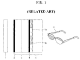
- FIG. 1 illustrates a related art patterned retarder type stereoscopic image display.
- the patterned retarder type stereoscopic image display implements a 3D image using polarization characteristic of a patterned retarder 5 disposed on a display panel 3 and polarization characteristic of polarization glasses 6 a user wears.
- the patterned retarder type stereoscopic image display displays a left eye image L and a right eye image R on adjacent lines of the display panel 3 and switches polarization characteristics of light incident on the polarization glasses 6 through the patterned retarder 5 .
- the patterned retarder type stereoscopic image display allows polarization characteristic of the left eye image L to be different from polarization characteristic of the right eye image R and spatially divides the left eye image L and the right eye image R the user sees, thereby implementing the 3D image.
- a reference numeral 1 denotes a backlight unit providing light to the display panel 3
- reference numerals 2 and 4 denote polarizing films, that are respectively attached to an upper substrate and a lower substrate of the display panel 3 so as to select linear polarization.
- the patterned retarder type stereoscopic image display shown in FIG. 1 visibility of the 3D image is degraded because of a crosstalk generated at a position of a vertical viewing angle.
- the user's left eye has to transmit only light of the left eye image L and the user's right eye has to transmit only light of the right eye image R, so that the user can sufficiently feel a stereoscopic feeling of the 3D image.
- both the light of the left eye image L and the light of the right eye image R are incident on the user's left and right eyes, the user sees both the light of the left eye image L and the light of the right eye image R through the user's left or right eye, thereby perceiving the crosstalk.
- the crosstalk is generated at the vertical viewing angle, that is equal to or greater than a predetermined angle.
- the related art patterned retarder type stereoscopic image display has the very narrow vertical viewing angle at which the user can view the 3D image without the crosstalk.
- Japanese Laid Open Publication No. 2002-185983 discloses a method for widening an vertical viewing angle of a stereoscopic image display by forming black stripes BS in a patterned retarder 5 .
- an vertical viewing angle ⁇ at which the crosstalk is not theoretically generated, depends on the size of black matrixes BM of a display panel 3 , the size of the black stripes BS of the patterned retarder 5 , and a distance S between the display panel 3 and the patterned retarder 5 .
- the vertical viewing angle a widens as the size of the black matrixes BM and the size of the black stripes BS increase and as the distance S between the display panel 3 and the patterned retarder 5 decreases.
- a luminance of the stereoscopic image display including the black stripes BS formed in the patterned retarder 5 is much less than a luminance of the existing display device displaying only a two-dimensional (2D) image because of the black stripes BS.
- the stereoscopic image display including the black stripes BS formed in the patterned retarder 5 requires the precision alignment when the patterned retarder 5 is attached to the display panel 3 .
- the patterned retarder 5 is not accurately aligned, operations of the black stripes BS are not smoothly performed. Therefore, the user may view the left eye image through his/her right eye or may view the right eye image through his/her left eye. As a result, the user may perceive the crosstalk.
- a technology for controlling pixels of the display panel using active black stripes has been proposed, so as to solve the problems of the stereoscopic image display disclosed in Japanese Laid Open Publication No. 2002-185983.
- a stereoscopic image display includes a data display unit including a first scan transistor, the first scan transistor supplying a 2D data voltage of a data line to a pixel electrode in response to a gate pulse of a (2n ⁇ 1)th gate line in a 2D mode and supplying a 3D data voltage of the data line to the pixel electrode in response to the gate pulse of the (2n ⁇ 1)th gate line in a 3D mode, where n is a natural number, an active black stripe unit including a second transistor and a third transistor, the second transistor supplying the 2D data voltage of the data line to the pixel electrode in response to the gate pulse of the (2n ⁇ 1)th gate line in the 2D mode and supplying the 3D data voltage of the data line to the pixel electrode in response to the gate pulse of the (2n ⁇ 1)th gate line in the 3D mode, the third transistor being turned off in response to a low logic level voltage of a (2n)th gate line in the 2D mode and supplying a common voltage commonly applied to a common electrode to the
- a method for driving a stereoscopic image display including supplying a 2D data voltage of a data line to a pixel electrode of a data display part and a pixel electrode of a active black stripe part in response to a gate pulse of a (2n ⁇ 1)th gate line in a 2D mode, where n is a natural number; supplying a 3D data voltage of the data line to the pixel electrode of the data display part and the pixel electrode of the active black stripe part in response to the gate pulse of the (2n ⁇ 1)th gate line in a 3D mode; supplying a common voltage commonly applied to a common electrode to the pixel electrode in response to a gate pulse of the (2n)th gate line in the 3D mode; and sequentially supplying the gate pulse to the (2n ⁇ 1)th gate lines and sequentially supplying the gate pulse to the (2n)th gate lines.
- FIG. 1 illustrates a related art patterned retarder type stereoscopic image display
- FIG. 2 illustrates a related art stereoscopic image display in which black stripes are formed in a patterned retarder
- FIG. 3 is a block diagram schematically illustrating a stereoscopic image display according to an exemplary embodiment of the invention
- FIG. 4 is an exploded perspective view illustrating a display panel, a patterned retarder, and polarization glasses
- FIG. 5 is a block diagram illustrating in detail a configuration of a display device based on a Gate Driver-IC In Panel (GIP) driving manner;
- GIP Gate Driver-IC In Panel
- FIG. 6 is a circuit diagram illustrating in detail some of pixels of a display panel controlled by active black stripes according to an exemplary embodiment of the invention
- FIGS. 7A and 7B illustrate voltages of a pixel electrode and a common electrode of each of pixels of a display panel in a 2D mode and a 3D mode;
- FIG. 8 is a block diagram illustrating in detail a configuration of a shift register according to an exemplary embodiment of the invention.
- FIG. 9 illustrates an example of a circuit configuration of an A-stage shown in FIG. 8 ;
- FIG. 10 is a waveform diagram illustrating an example of input and output signals of an A-stage and a B-stage in a 2D mode according to an exemplary embodiment of the invention
- FIG. 11 is a waveform diagram illustrating another example of input and output signals of an A-stage and a B-stage in a 2D mode according to an exemplary embodiment of the invention.
- FIG. 12 is a waveform diagram illustrating input and output signals of an A-stage and a B-stage in a 3D mode according to an exemplary embodiment of the invention.
- Names of elements used in the following description may be selected in consideration of facility of specification preparation. Thus, the names of the elements may be different from names of elements used in a real product.
- FIG. 3 is a block diagram schematically illustrating a stereoscopic image display according to an example embodiment of the invention.
- FIG. 4 is an exploded perspective view illustrating a display panel, a patterned retarder, and polarization glasses.
- FIG. 5 is a block diagram illustrating in detail a configuration of a display device based on a Gate Driver-IC In Panel (GIP) driving manner.
- the stereoscopic image display according to the example embodiment of the invention may be implemented as a flat panel display such as a liquid crystal display (LCD), a field emission display (FED), a plasma display panel (PDP), and an organic light emitting diode (OLED) display.
- the example embodiment of the invention describes the liquid crystal display as an example of the stereoscopic image display. Other kinds of flat panel displays may be used.
- the stereoscopic image display includes a display panel 10 , polarization glasses 20 , a gate driver 110 , a data driver 120 , a timing controller 130 , a host system 140 , and the like.
- the display panel 10 displays an image under the control of the timing controller 130 .
- the display panel 10 includes a thin film transistor (TFT) substrate, a color filter substrate, and a liquid crystal layer between the TFT substrate and the color filter substrate.
- TFT thin film transistor
- Data lines and gate lines are formed on the TFT substrate to cross each other, and a plurality of liquid crystal cells are arranged in a plurality of cell regions defined by the data lines and the gate lines in a matrix form.
- a TFT formed at each of crossings of the data lines and the gate lines transfers a data voltage supplied via the data line to a pixel electrode of the liquid crystal cell in response to a gate pulse received through the gate line.
- a gate electrode of the TFT is connected to the gate line
- a source electrode of the TFT is connected to the data line
- a drain electrode of the TFT is connected to the pixel electrode of the liquid crystal cell and a storage capacitor.
- the storage capacitor holds the data voltage transferred to the pixel electrode for a predetermined time until a next data voltage enters.
- a common voltage is supplied to a common electrode opposite the pixel electrode.
- the color filter substrate includes black matrixes and color filters.
- the common electrode is formed on the color filter substrate in a vertical electric field driving manner such as a twisted nematic (TN) mode and a vertical alignment (VA) mode.
- the common electrode is formed on the TFT substrate along with the pixel electrode in a horizontal electric field driving manner such as an in-plane switching (IPS) mode and a fringe field switching (FFS) mode.
- IPS in-plane switching
- FFS fringe field switching
- an upper polarizing plate 11 a is attached to the color filter substrate of the display panel 10
- a lower polarizing plate 11 b is attached to the TFT substrate of the display panel 10
- a light transmission axis r 1 of the upper polarizing plate 11 a is perpendicular to a light transmission axis r 2 of the lower polarizing plate 11 b .
- Alignment layers for setting pre-tilt angles of liquid crystals are respectively formed on the TFT substrate and the color filter substrate of the display panel 10 .
- a spacer is formed between the TFT substrate and the color filter substrate of the display panel 10 so as to provide a cell gap of the liquid crystal layer.
- the display panel 10 may be implemented in any liquid crystal mode as well as the TN, VA, IPS, and FFS modes.
- Each of pixels of the display panel 10 includes a red subpixel, a green subpixel, and a blue subpixel.
- Each of the red subpixel, the green subpixel, and the blue subpixel includes a data display part and an active black stripe part. This is described in detail below with reference to FIG. 6 .
- pixels of odd-numbered lines of the display panel 10 and pixels of even-numbered lines of the display panel 10 display a 2D image.
- pixels of the odd-numbered lines of the display panel 10 display a left eye image (or a right eye image)
- the pixels of the even-numbered lines of the display panel 10 display the right eye image (or the left eye image).
- Light of the image displayed on the pixels of the display panel 10 is incident on a patterned retarder 30 disposed on the display panel 10 through the upper polarizing plate 11 a.
- first retarders 31 are formed on odd-numbered lines of the patterned retarder 30
- second retarders 32 are formed on even-numbered lines of the patterned retarder 30 .
- the pixels of the odd-numbered lines of the display panel 10 are positioned opposite the first retarders 31 formed on the odd-numbered lines of the patterned retarder 30
- the pixels of the even-numbered lines of the display panel 10 are positioned opposite the second retarders 32 formed on the even-numbered lines of the patterned retarder 30 .
- the first retarders 31 retard a phase of light from the display panel 10 by + ⁇ /4, where A is a wavelength of light.
- the second retarders 32 retard a phase of the light from the display panel 10 by ⁇ /4.
- An optical axis r 3 of the first retarder 31 is perpendicular to an optical axis r 4 of the second retarder 32 .
- the first retarders 31 may be configured so as to pass through only first circularly polarized light (for example, left-circularly polarized light), and the second retarders 32 may be configured so as to pass through only second circularly polarized light (for example, right-circularly polarized light).
- a left eye polarization filter of the polarization glasses 20 has the same optical axis as the first retarder 31 of the patterned retarder 30
- a right eye polarization filter of the polarization glasses 20 has the same optical axis as the second retarder 32 of the patterned retarder 30
- a left circular polarization filter may be selected as the left eye polarization filter of the polarization glasses 20
- a right circular polarization filter may be selected as the right eye polarization filter of the polarization glasses 20 .
- a user has to wear the polarization glasses 20 when viewing a 3D image, and has to remove the polarization glasses 20 when viewing a 2D image.
- the left eye image displayed on the pixels of the odd-numbered lines of the display panel 10 passes through the first retarder 31 and is converted into the left-circularly polarized light
- the right eye image displayed on the pixels of the even-numbered lines of the display panel 10 passes through the second retarder 32 and is converted into the right-circularly polarized light.
- the left-circularly polarized light passes through the left eye polarization filter of the polarization glasses 20 and reaches the user's left eye
- the right-circularly polarized light passes through the right eye polarization filter of the polarization glasses 20 and reaches the user's right eye.
- the user views only the left eye image through his or her left eye and views only the right eye image through his/her right eye.
- the data driver 120 includes a plurality of source driver integrated circuits (ICs) 70 .
- the source driver ICs 70 convert image data RGB received from the timing controller 130 into positive and negative gamma compensation voltages and generate positive and negative analog data voltages.
- the source driver ICs 70 then supply the positive and negative analog data voltages to the data lines of the display panel 10 .
- the gate driver 110 sequentially supplies the gate pulse synchronized with the data voltage to the gate lines of the display panel 10 under the control of the timing controller 130 .
- the gate driver 110 includes a level shifter 40 , a shift register 50 , and the like.
- the level shifter 40 level-shifts a transistor-transistor-logic (TTL) level voltage of clocks CLK received from the timing controller 110 to a gate high voltage VGH and a gate low voltage VGL.
- TTL transistor-transistor-logic
- the level shifter 40 is mounted on a printed circuit board (PCB) 60 , and the shift register 50 is directly formed on the TFT substrate of the display panel 10 .
- the shift register 50 is described in detail below with reference to FIGS. 7 and 8 .
- a backlit liquid crystal display panel modulating light from a backlight unit may be generally selected as the display panel 10 .
- the backlight unit includes a plurality of light sources, that are turned on based on a driving current supplied by a backlight unit driver, a light guide plate (or a diffusion plate), a plurality of optical sheets, and the like.
- the backlight unit may be implemented as one of an edge type backlight unit and a direct type backlight unit.
- the light sources of the backlight unit may include one or at least two of a hot cathode fluorescent lamp (HCFL), a cold cathode fluorescent lamp (CCFL), an external electrode fluorescent lamp (EEFL), and a light emitting diode (LED).
- HCFL hot cathode fluorescent lamp
- CCFL cold cathode fluorescent lamp
- EEFL external electrode fluorescent lamp
- LED light emitting diode
- the backlight unit driver generates the driving current for turning on the light sources of the backlight unit.
- the backlight unit driver switches on or off the driving current supplied to the light sources under the control of the timing controller 130 .
- the timing controller 130 outputs backlight control data, that adjusts a backlight luminance and a turn-on timing of the light sources in response to a global or local dimming signal received from the host system 140 , to the backlight unit driver in a serial peripheral interface (SPI) data format.
- SPI serial peripheral interface
- the timing controller 130 receives the image data RGB and timing signals such as a vertical sync signal Vsync, a horizontal sync signal Hsync, a data enable DE, and clocks CLK from the host system 140 .
- the timing controller 130 outputs a gate control signal for controlling the gate driver 110 to the gate driver 110 and outputs a data control signal for controlling the data driver 120 to the data driver 120 based on the timing signals.
- the gate control signal includes first and second start voltages VST 1 and VST 2 , clocks CLK, and the like.
- the first start voltage VST 1 controls an output timing of a first gate pulse of an A-stage of the shift register 50 .
- the second start voltage VST 2 controls an output timing of a first gate pulse of a B-stage of the shift register 50 .
- the clocks CLK may be i-phase clocks, where ‘i’ is a natural number equal to or greater than 3.
- the clocks CLK are input to the shift register 50 and control an output of the shift register 50 .
- the data control signal includes a source start pulse SSP, a source sampling clock SSC, a polarity control signal POL, a source output enable SOE, and the like.
- the source start pulse SSP controls a data sampling start time point of the data driver 120 .
- the source sampling clock SSC controls a sampling operation of the data driver 120 based on a rising or falling edge thereof. If digital video data to be input to the data driver 120 is transferred based on a mini low voltage differential signaling (LVDS) interface standard, the source start pulse SSP and the source sampling clock SSC may be omitted.
- the polarity control signal POL inverts a polarity of the data voltage output by the data driver 120 every L horizontal periods, where L is a natural number.
- the source output enable SOE controls an output timing of the data driver 120 .
- the host system 140 supplies the image data RGB to the timing controller 130 through an interface such as an LVDS interface and a transition minimized differential signaling (TMDS) interface. Further, the host system 140 supplies the timing signals Vsync, Hsync, DE, and CLK and a mode signal MODE to the timing controller 130 .
- the mode signal MODE distinguishes the 2D mode from the 3D mode.
- FIG. 6 is a circuit diagram illustrating in detail some of pixels of the display panel controlled by active black stripes according to the example embodiment of the invention.
- the display panel 10 includes j ⁇ k pixels 200 , where j and k are a positive integer equal to or greater than 2.
- Each of the j ⁇ k pixels 200 includes a red subpixel R, a green subpixel G, and a blue subpixel B.
- Each of the red, green, and blue subpixels R, G, and B includes a data display part 210 and an active black stripe part 220 .
- a liquid crystal cell of the data display part 210 is connected to a first scan TFT 211 and is driven by an electric field between a pixel electrode 240 and a common electrode 250 of the data display part 210 .
- the first scan TFT 211 supplies a data voltage of a data line D 1 , D 2 , or D 3 to the pixel electrode 240 of the data display part 210 in response to a gate pulse of a (2n ⁇ 1)th gate line G 1 or G 3 , where n is a natural number.
- a gate electrode of the first scan TFT 211 is connected to the (2n ⁇ 1)th gate line G 1 or G 3 , a drain electrode of the first scan TFT 211 is connected to the data line D 1 , D 2 , or D 3 , and a source electrode of the first scan TFT 211 is connected to the pixel electrode 240 of the data display part 210 .
- a liquid crystal cell of the active black stripe part 220 is connected to a second scan TFT 221 and a third scan TFT 222 and is driven by an electric field between a pixel electrode 240 and a common electrode 250 of the active black stripe part 220 .
- the second scan TFT 221 supplies the data voltage of the data line D 1 , D 2 , or D 3 to the pixel electrode 240 of the active black stripe part 220 in response to the gate pulse of the (2n ⁇ 1)th gate line G 1 or G 3 .
- a gate electrode of the second scan TFT 221 is connected to the (2n ⁇ 1)th gate line G 1 or G 3 , a drain electrode of the second scan TFT 221 is connected to the data line D 1 , D 2 , or D 3 , and a source electrode of the second scan TFT 221 is connected to the pixel electrode 240 of the active black stripe part 220 .
- the third scan TFT 222 In the 2D mode, because the gate pulse is not supplied to a (2n)th gate line G 2 or G 4 , the third scan TFT 222 remains in a turned-off state. In the 3D mode, the third scan TFT 222 supplies a common voltage Vcom from a common voltage line 250 to the pixel electrode 240 of the active black stripe part 220 in response to the gate pulse of the (2n)th gate line G 2 or G 4 .
- a gate electrode of the third scan TFT 222 is connected to the (2n)th gate line G 2 or G 4
- a drain electrode of the third scan TFT 222 is connected to the common voltage line 250
- a source electrode of the third scan TFT 222 is connected to the pixel electrode 240 of the active black stripe part 220 .
- the shift register 50 includes A-stages ST A ( 1 ) and ST A ( 2 ) and B-stages ST B ( 1 ) and ST B ( 2 ).
- the A-stages ST A ( 1 ) and ST A ( 2 ) sequentially output the gate pulse to the (2n-1)th gate lines G 1 and G 3
- the B-stages ST B ( 1 ) and ST B ( 2 ) sequentially output the gate pulse to the (2n)th gate lines G 2 and G 4 .
- the A-stages ST A ( 1 ) and ST A ( 2 ) sequentially output the gate pulse to the (2n ⁇ 1)th gate lines G 1 and G 3 , but the B-stages ST B ( 1 ) and ST B ( 2 ) do not output the gate pulse to the (2n)th gate lines G 2 and G 4 .
- the A-stages ST A ( 1 ) and ST A ( 2 ) sequentially output the gate pulse to the (2n ⁇ 1)th gate lines G 1 and G 3
- the B-stages ST B ( 1 ) and ST B ( 2 ) may sequentially output the gate pulse to the (2n)th gate lines G 2 and G 4 .
- the output of the B-stages ST B ( 1 ) and ST B ( 2 ) is earlier than the output of the A-stages ST A ( 1 ) and ST A ( 2 ) by a predetermined time.
- the A-stages ST A ( 1 ) and ST A ( 2 ) sequentially output the gate pulse to the (2n ⁇ 1)th gate lines G 1 and G 3
- the B-stages ST B ( 1 ) and ST B ( 2 ) sequentially output the gate pulse to the (2n)th gate lines G 2 and G 4 .
- the output of the A-stages ST A ( 1 ) and ST A ( 2 ) is earlier than the output of the B-stages ST B ( 1 ) and ST B ( 2 ) by a predetermined time.
- the data driver 120 In the 2D mode, the data driver 120 outputs the data voltage of the 2D image to the data lines D 1 to D 3 in synchronization with the gate pulse of the (2n ⁇ 1)th gate lines G 1 and G 3 . Thus, the data voltage of the 2D image is supplied to the data display part 210 and the active black stripe part 220 .
- the data driver 120 In the 3D mode, the data driver 120 outputs the data voltage of the 3D image to the data lines D 1 to D 3 in synchronization with the gate pulse of the gate lines G 1 to G 4 .
- the data voltage of the 3D image is supplied to the data display part 210 and the active black stripe part 220 .
- the common voltage Vcom is supplied to the active black stripe part 220 by the gate pulse of the (2n)th gate lines G 2 and G 4 .
- the data display part 210 and the active black stripe part 220 are charged to the red, green, and blue data voltages of the 2D image.
- the data display part 210 is charged to the red, green, and blue data voltages of the 3D image, and the active black stripe part 220 is charged to the common voltage Vcom.
- FIGS. 7A and 7B illustrate voltages of the pixel electrode and the common electrode of each of the data display part and the active black stripe part in the 2D mode and the 3D mode.
- the pixel electrode of each of the data display part 210 and the active black stripe part 220 is charged to the data voltage.
- the pixel electrode of the data display part 210 is charged to the data voltage, but the pixel electrode of the active black stripe part 220 is charged to the common voltage Vcom.
- the active black stripe part 220 is charged to the data voltage of the 2D image, thereby increasing a luminance and a chrominance of the 2D image. Hence, the display quality of the 2D image is improved.
- the active black stripe part 220 is charged to the common voltage Vcom and displays a black image, thereby serving as a black stripe.
- the configuration and the operation of the shift register 50 are described below. More specifically, a method for charging the pixel electrode of each of the data display part 210 and the active black stripe part 220 to the data voltage in the 2D mode, and for charging the pixel electrode of the data display part 210 the data voltage and the pixel electrode of the active black stripe part 220 to the common voltage Vcom in the 3D mode.
- FIG. 8 is a block diagram illustrating in detail the configuration of the shift register according to the example embodiment of the invention.
- the shift register 50 includes a plurality of cascade-connected A-stages ST A ( 1 ) to ST A (n) and a plurality of cascade-connected B-stages ST B ( 1 ) to ST B (n).
- Each of the A-stages ST A ( 1 ) to ST A (n) and each of the B-stages ST B ( 1 ) to ST B (n) have one output channel and output one gate pulse.
- the gate pulse is applied to the gate lines of the display panel 10 , and at the same time, serves as a carry signal transferred to a front stage and a rear stage.
- the front stage is referred to as a stage positioned in front of a base stage
- the rear stage is referred to as a stage positioned in rear of the base stage.
- k is a natural number (i.e., equal to or greater than 2) within the range of 1 ⁇ k ⁇ n
- the front stage indicates one of the first A-stage ST A ( 1 ) to the (k ⁇ 1)th A-stage ST A (k ⁇ 1)
- the rear stage indicates one of the (k+1)th A-stage ST A (k+1) to the nth A-stage ST A (n).
- the front stage indicates one of the first B-stage ST B ( 1 ) to the (k ⁇ 1)th B-stage ST B (k ⁇ 1) and the rear stage indicates one of the (k+1) B-stage ST B (k+1) to the nth B-stage ST B (n).
- each of the plurality of cascade-connected A-stages ST A ( 1 ) to ST A (n) serves as a carry signal of the rear stage. Therefore, when the first start voltage VST 1 is supplied to the A-stages ST A ( 1 ) to ST A (n), the A-stages ST A ( 1 ) to ST A (n) sequentially supply the gate pulses to the (2n ⁇ 1)th gate lines. When the first start voltage VST 1 is not supplied, the A-stages ST A ( 1 ) to ST A (n) do not supply the gate pulse to the (2n ⁇ 1)th gate lines. Further, the output of each of the plurality of cascade-connected B-stages ST B ( 1 ) to ST B (n) serves as a carry signal of the rear stage.
- the B-stages ST B ( 1 ) to ST B (n) sequentially supply the gate pulses to the (2n)th gate lines.
- the B-stages ST B ( 1 ) to ST B (n) do not supply the gate pulse to the (2n)th gate lines.
- the A-stages ST A ( 1 ) to ST A (n) output gate pulses Gout( 1 ) to Gout(2n ⁇ 1) in order from the first A-stage ST A ( 1 ) to the nth A-stage ST A (n). Namely, an output terminal of the kth A-stage ST A (k) is connected to a (2k ⁇ 1)th gate line and outputs a (2k ⁇ 1)th gate pulse.
- Each of the A-stages ST A ( 1 ) to ST A (n) operates in response to a carry signal of one front stage applied as a start signal to a first input terminal VST and a carry signal of one rear stage applied as a reset signal to a second input terminal VRESET.
- the B-stages ST B ( 1 ) to ST B (n) output gate pulses Gout( 2 ) to Gout( 2 n ) in order from the first B-stage ST B ( 1 ) to the nth B-stage ST B (n). Namely, an output terminal of the kth B-stage ST B (k) is connected to a (2k)th gate line and outputs a (2k)th gate pulse.
- Each of the B-stages ST B ( 1 ) to ST B (n) operates in response to a carry signal of one front stage applied as a start signal to a first input terminal VST and a carry signal of one rear stage applied as a reset signal to a second input terminal VRESET.
- FIGS. 10 to 12 illustrate 6-phase clocks CLK 1 to CLK 6 , but are not limited thereto.
- Each of the 6-phase clocks CLK 1 to CLK 6 has a pulse width of one horizontal period and swings between the gate high voltage VGH and the gate low voltage VGL.
- a power voltage VDD and a ground level voltage GND, or a low potential voltage VSS of the gate low voltage VGL are supplied to each of the A-stages ST A ( 1 ) to ST A (n) and each of the B-stages ST B ( 1 ) to ST B (n).
- the gate high voltage VGH is set to a voltage equal to or greater than a threshold voltage of TFTs formed in an active array of the display panel 10 .
- the gate low voltage VGL is set to a voltage less than a threshold voltage of TFTs formed in a TFT array of the display panel 10 .
- the gate high voltage VGH may be set to about 20V to 30V, and the gate low voltage VGL may be set to about ⁇ 5V.
- FIG. 9 illustrates an example of a circuit configuration of the A-stage shown in FIG. 8 . Since a circuit configuration of the B-stage is substantially the same as the circuit configuration of the A-stage, a further description may be briefly made or may be entirely omitted. As shown in FIG. 9 , one of the 6-phase clocks is input to a clock terminal CLK of each of the A-stages ST A ( 1 ) to ST A (n).
- Each of the A-stages ST A ( 1 ) to ST A (n) includes a Q node charging unit, that charges a Q node in response to a signal input through the first input terminal VST, a node controller for controlling charging and discharging operations of the Q node and a QB node, a Q node discharging unit, that discharges the Q node in response to a signal input through the second input terminal VRESET, and an output unit for outputting the gate pulse based on voltages of the Q node and the QB node.
- the Q node charging unit includes a first TFT T 1 for charging the Q node.
- the first TFT T 1 applies the power voltage VDD to the Q node in response to the start signal input through the first input terminal VST.
- An output Gout(2k ⁇ 7) of a (k ⁇ 3)th A-stage ST A (k ⁇ 3) as the start signal is input to the first TFT T 1 of the kth A-stage ST A (k).
- the first start voltage VST as the start signal is input to the first TFTs T 1 of the first and second A-stages ST A ( 1 ) and ST A ( 2 ).
- a gate electrode of the first TFT T 1 is connected to the first input terminal VST, a drain electrode of the first TFT T 1 is connected to an input terminal of the power voltage VDD, and a source electrode of the first TFT T 1 is connected to the Q node.
- the node controller includes a second TFT T 2 for controlling the Q node and third to seventh TFTs T 3 to T 7 for controlling the QB node.
- the second TFT T 2 discharges the Q node to the low potential voltage VSS based on the voltage of the QB node.
- a gate electrode of the second TFT T 2 is connected to the QB node, a drain electrode of the second TFT T 2 is connected to the Q node, and a source electrode of the second TFT T 2 is connected to an input terminal of the low potential voltage VSS.
- the third TFT T 3 is diode-connected and applies the power voltage VDD to a first node N 1 .
- a gate electrode and a drain electrode of the third TFT T 3 are connected to the input terminal of the power voltage VDD, and a source electrode of the third TFT T 3 is connected to the first node Ni.
- the fourth TFT T 4 switches on or off a current path between the first node N 1 and the input terminal of the low potential voltage VSS based on the voltage of the Q node.
- a gate electrode of the fourth TFT T 4 is connected to the Q node, a drain electrode of the fourth TFT T 4 is connected to the first node N 1 , and a source electrode of the fourth TFT T 4 is connected to the input terminal of the low potential voltage VSS.
- the fifth TFT T 5 discharges the QB node to the low potential voltage VSS based on the voltage of the Q node.
- a gate electrode of the fifth TFT T 5 is connected to the Q node, a drain electrode of the fifth TFT T 5 is connected to the QB node, and a source electrode of the fifth TFT T 5 is connected to the input terminal of the low potential voltage VSS.
- the sixth TFT T 6 charges the QB node to the power voltage VDD based on the voltage of the first node N 1 .
- a gate electrode of the sixth TFT T 6 is connected to the first node N 1 , a drain electrode of the sixth TFT T 6 is connected to an input terminal VDD_O of the power voltage VDD, and a source electrode of the sixth TFT T 6 is connected to the QB node.
- the seventh TFT T 7 discharges the QB node to the low potential voltage VSS in response to the start signal input through the first input terminal VST.
- a gate electrode of the seventh TFT T 7 is connected to the first input terminal VST, a drain electrode of the seventh TFT T 7 is connected to the QB node, and a source electrode of the seventh TFT T 7 is connected to the input terminal of the low potential voltage VSS.
- the Q node discharging unit includes an eighth TFT T 8 for discharging the Q node.
- the eighth TFT T 8 discharges the Q node to the low potential voltage VSS in response to the start signal input through the second input terminal VRESET.
- An output Gout(2k+5) of a (k+3)th A-stage ST A (k+3) as the reset signal is input to the eighth TFT T 8 of the kth A-stage ST A (k).
- the first start voltage VST as the reset signal is input to the eighth TFTs T 8 of the (n ⁇ 1)th and nth A-stages ST A (n ⁇ 1) and ST A (n).
- a gate electrode of the eighth TFT T 8 is connected to the second input terminal VRESET, a drain electrode of the eighth TFT T 8 is connected to the Q node, and a source electrode of the eighth TFT T 8 is connected to the input terminal of the power voltage VDD.
- the output unit includes a pull-up TFT TU and a pull-down TFT TD that generate an output of the gate pulse.
- the pull-up TFT TU is turned on based on the voltage of the Q node and charges an output node NO to a clock input through the clock terminal CLK.
- the pull-down TFT TD is turned on based on the voltage of the QB node and discharges the output node NO to the low potential voltage VSS.
- the pull-up TFT TU is turned on due to bootstrapping of the Q node and thus charges the output node NO to the clock input through the clock terminal CLK to thereby generate the gate pulse.
- a gate electrode of the pull-up TFT TU is connected to the Q node
- a drain electrode of the pull-up TFT TU is connected to the clock terminal CLK
- a source electrode of the pull-up TFT TU is connected to the output node NO.
- the pull-down TFT TD discharges the output node NO to the low potential voltage VSS based on the voltage of the QB node, so as to hold the output of the gate pulse in a falling state.
- a gate electrode of the pull-down TFT TD is connected to the QB node, a drain electrode of the pull-down TFT TD is connected to the output node NO, and a source electrode of the pull-down TFT TD is connected to the input terminal of the low potential voltage VSS.
- a (2k ⁇ 1)th gate pulse Gout(2k ⁇ 1) output from the kth A-stage ST A (k) is input to the second input terminal VRESET of a (k ⁇ 3)th A-stage ST A (k ⁇ 3) and the first input terminal VST of the (k+3)th A-stage ST A (k+3).
- FIG. 10 is a waveform diagram illustrating an example of input and output signals of the A-stage and the B-stage in the 2D mode according to the example embodiment of the invention.
- the first and second start voltages VST 1 and VST 2 are generated, and the 6-phase clocks CLK 1 to CLK 6 are generated as cycle clocks, that are sequentially retarded in order from the first clock CLK 1 to the sixth clock CLK 6 .
- the first start voltage VST 1 or a (2k ⁇ 7)th output Gout(2k ⁇ 7) as the start signal is input to the kth A-stage ST A (k) through the first input terminal VST.
- the first TFT T 1 is turned on in response to the first start voltage VST 1 or the (2k ⁇ 7)th output Gout(2k ⁇ 7).
- the Q node is charged to the gate high voltage VGH, and the QB node is discharged to the gate low voltage VGL.
- the Q node is held at the gate high voltage VGH, and the QB node is held at the gate low voltage VGL.
- the first gate shift clock CLK 1 is applied to the drain electrode of the pull-up TFT TU. Because the Q node is bootstrapped due to a parasitic capacitance between the gate electrode and the drain electrode of the pull-up TFT TU, the voltage of the Q node increases to a voltage level VGH′ greater than the gate high voltage VGH and turns on the pull-up TFT TU. Thus, the voltage of the output node NO increases to the gate high voltage VGH and rises the (2k ⁇ 1)th gate pulse Gout(2k ⁇ 1), and the QB node is held at the gate low voltage VGL.
- the Q node is held at the gate high voltage VGH, and the QB node is held at the gate low voltage VGL.
- the first start voltage VST 1 or a (2k+5)th output Gout(2k+5) as the reset signal is input to the kth A-stage ST A (k) through the second input terminal VRESET.
- the eighth TFT T 8 is turned on in response to the first start voltage VST 1 or the (2k+5)th output Gout(2k+5).
- the Q node is discharged to the gate low voltage VGL. Because the fourth TFT T 4 and the fifth TFT T 5 are turned off due to the discharging operation of the Q node, the QB node is charged to the power voltage VDD of the gate high voltage VGH applied through the sixth TFT T 6 .
- the pull-down TFT TD is turned on due to the charging operation of the QB node. Hence, the voltage of the output node NO falls to the gate low voltage VGL, and the (2k ⁇ 1)th gate pulse Gout(2k ⁇ 1) is held at the gate low voltage VGL.
- the second start voltage VST 2 is not applied to the B-stages ST B ( 1 ) to ST B (n). Because the start signal is not input to the first input terminal VST of the kth B-stage ST B (k), the Q node of the kth B-stage ST B (k) is held at the gate low voltage VGL and the QB node is held at the gate high voltage VGH. Further, the kth B-stage ST B (k) holds a (2k)th gate pulse Gout(2k) to the gate low voltage VGL.
- each of the A-stages ST A ( 1 ) to ST A (n) outputs the gate pulse to the (2n ⁇ 1)th gate lines, and the B-stages ST B ( 1 ) to ST B (n) do not output the gate pulse to the (2n)th gate lines.
- the pixel electrode of the data display part 210 is charged to the data voltage due to the turn-on operation of the first scan TFT 211 of the data display part 210 as shown in FIG. 7A .
- the pixel electrode of the active black stripe part 220 is charged to the data voltage as shown in FIG. 7A .
- the data display part 210 and the active black stripe part 220 display the 2D image.
- FIG. 11 is a waveform diagram illustrating another example of input and output signals of the A-stage and the B-stage in the 2D mode according to the example embodiment of the invention.
- the first and second start voltages VST 1 and VST 2 are generated, and the 6-phase clocks CLK 1 to CLK 6 are generated as cycle clocks, that are sequentially retarded in order from the first clock CLK 1 to the sixth clock CLK 6 .
- FIG. 11 illustrates the second start voltage VST 2 , that is generated earlier than the first start voltage VST 1 by four horizontal periods, but is not limited thereto.
- the second start voltage VST 2 may be generated earlier than the first start voltage VST 1 by three horizontal periods to several tens of horizontal periods.
- the Q node is held at the gate low voltage VGL, and the QB node is held at the gate high voltage VGH.
- the first start voltage VST 1 or the (2k ⁇ 7)th output Gout(2k ⁇ 7) as the start signal is input to the kth A-stage ST A (k) through the first input terminal VST.
- the first TFT T 1 is turned on in response to the first start voltage VST 1 or the (2k ⁇ 7)th output Gout(2k ⁇ 7).
- the Q node is charged to the gate high voltage VGH, and the QB node is discharged to the gate low voltage VGL.
- the Q node is held at the gate high voltage VGH, and the QB node is held at the gate low voltage VGL.
- the fifth gate shift clock CLK 5 is applied to the drain electrode of the pull-up TFT TU. Because the Q node is bootstrapped due to the parasitic capacitance between the gate electrode and the drain electrode of the pull-up TFT TU, the voltage of the Q node increases to the voltage level VGH′ greater than the gate high voltage VGH and turns on the pull-up TFT TU. Thus, the voltage of the output node NO increases to the gate high voltage VGH and rises the (2k ⁇ 1)th gate pulse Gout(2k ⁇ 1), and the QB node is held at the gate low voltage VGL.
- the Q node is held at the gate high voltage VGH, and the QB node is held at the gate low voltage VGL.
- the first start voltage VST 1 or the (2k+5)th output Gout(2k+5) as the reset signal is input to the kth A-stage ST A (k) through the second input terminal VRESET.
- the eighth TFT T 8 is turned on in response to the first start voltage VST 1 or the (2k+5)th output Gout(2k+5).
- the Q node is discharged to the gate low voltage VGL. Because the fourth TFT T 4 and the fifth TFT T 5 are turned off due to the discharging operation of the Q node, the QB node is charged to the power voltage VDD of the gate high voltage VGH applied through the sixth TFT T 6 .
- the pull-down TFT TD is turned on due to the charging operation of the QB node. Hence, the voltage of the output node NO falls to the gate low voltage VGL, and the (2k ⁇ 1)th gate pulse Gout(2k ⁇ 1) is held at the gate low voltage VGL.
- the second start voltage VST 2 or a (2k ⁇ 6)th output Gout(2k ⁇ 6) as the start signal is input to the kth B-stage ST B (k) through the first input terminal VST.
- the first TFT T1 is turned on in response to the second start voltage VST2 or the (2k ⁇ 6)th output Gout(2k ⁇ 6).
- the Q node is charged to the gate high voltage VGH, and the QB node is discharged to the gate low voltage VGL.
- the Q node is held at the gate high voltage VGH, and the QB node is held at the gate low voltage VGL.
- the first gate shift clock CLK 1 is applied to the drain electrode of the pull-up TFT TU. Because the Q node is bootstrapped due to the parasitic capacitance between the gate electrode and the drain electrode of the pull-up TFT TU, the voltage of the Q node increases to the voltage level VGH′ greater than the gate high voltage VGH and turns on the pull-up TFT TU. Thus, the voltage of the output node NO increases to the gate high voltage VGH and rises the (2k)th gate pulse Gout( 2 k ), and the QB node is held at the gate low voltage VGL.
- the voltage of the Q node is held at the gate high voltage VGH and the pull-up TFT TU is turned off.
- the (2k)th gate pulse Gout( 2 k ) falls to the gate low voltage VGL, and the QB node is held at the gate low voltage VGL.
- the Q node is held at the gate high voltage VGH, and the QB node is held at the gate low voltage VGL.
- the second start voltage VST 2 or the (2k+6)th output Gout(2k+6) as the reset signal is input to the kth B-stage ST B (k) through the second input terminal VRESET.
- the eighth TFT T 8 is turned on in response to the second start voltage VST 2 or the (2k+6)th output Gout(2k+6).
- the Q node is discharged to the gate low voltage VGL. Because the fourth TFT T 4 and the fifth TFT T 5 are turned off due to the discharging operation of the Q node, the QB node is charged to the power voltage VDD of the gate high voltage VGH applied through the sixth TFT T 6 .
- the pull-down TFT TD is turned on due to the charging operation of the QB node. Hence, the voltage of the output node NO falls to the gate low voltage VGL, and the (2k)th gate pulse Gout(2k) is held at the gate low voltage VGL.
- the Q node is held at the gate low voltage VGL, and the QB node is held at the gate high voltage VGH.
- each of the B-stages ST B ( 1 ) to ST B (n) outputs the gate pulse to the (2n)th gate lines.
- each of the A-stages ST A ( 1 ) to ST A (n) outputs the gate pulse to the (2n ⁇ 1)th gate lines.
- the pixel electrode of the data display part 210 is charged to the data voltage due to the turn-on operation of the first scan TFT 211 of the data display part 210 as shown in FIG. 7A . Further, the third scan TFT 222 of the active black stripe part 220 is turned on.
- the second scan TFT 221 of the active black stripe part 220 is turned on. Therefore, the pixel electrode of the active black stripe part 220 is discharged to the common voltage and then is charged to the data voltage as shown in FIG. 7A .
- the data display part 210 and the active black stripe part 220 display the 2D image.
- the QB node of the kth B-stage ST B (k) is continuously held at the gate high voltage VGH.
- the threshold voltage of the pull-down TFT TD connected to the QB node may shift because of a gate bias stress.
- the gate bias stress of the pull-down TFT TD connected to the QB node may be prevented.
- FIG. 12 is a waveform diagram illustrating input and output signals of the A-stage and the B-stage in the 3D mode according to the example embodiment of the invention.
- the first and second start voltages VST 1 and VST 2 are generated, and the 6-phase clocks CLK 1 to CLK 6 are generated as cycle clocks, that are sequentially retarded in order from the first clock CLK 1 to the sixth clock CLK 6 .
- FIG. 12 illustrates the first start voltage VST 1 , that is generated earlier than the second start voltage VST 2 by four horizontal periods, but is not limited thereto.
- the first start voltage VST 1 may be generated earlier than the second start voltage VST 2 by three horizontal periods to several tens of horizontal periods.
- the first start voltage VST 1 or the (2k ⁇ 7)th output Gout(2k ⁇ 7) as the start signal is input to the kth A-stage ST A (k) through the first input terminal VST.
- the first TFT T 1 is turned on in response to the first start voltage VST 1 or the (2k ⁇ 7)th output Gout(2k ⁇ 7).
- the Q node is charged to the gate high voltage VGH, and the QB node is discharged to the gate low voltage VGL.
- the Q node is held at the gate high voltage VGH, and the QB node is held at the gate low voltage VGL.
- the first gate shift clock CLK 1 is applied to the drain electrode of the pull-up TFT TU. Because the Q node is bootstrapped due to the parasitic capacitance between the gate electrode and the drain electrode of the pull-up TFT TU, the voltage of the Q node increases to the voltage level VGH′ greater than the gate high voltage VGH and turns on the pull-up TFT TU. Thus, the voltage of the output node NO increases to the gate high voltage VGH and rises the (2k ⁇ 1)th gate pulse Gout(2k ⁇ 1), and the QB node is held at the gate low voltage VGL.
- the Q node is held at the gate high voltage VGH, and the QB node is held at the gate low voltage VGL.
- the first start voltage VST 1 or the (2k+5)th output Gout(2k+5) as the reset signal is input to the kth A-stage ST A (k) through the second input terminal VRESET.
- the eighth TFT T 8 is turned on in response to the first start voltage VST 1 or the (2k+5)th output Gout(2k+5).
- the Q node is discharged to the gate low voltage VGL. Because the fourth TFT T 4 and the fifth TFT T 5 are turned off due to the discharging operation of the Q node, the QB node is charged to the power voltage VDD of the gate high voltage VGH applied through the sixth TFT T 6 .
- the pull-down TFT TD is turned on due to the charging operation of the QB node. Hence, the voltage of the output node NO falls to the gate low voltage VGL, and the (2k ⁇ 1)th gate pulse Gout(2k ⁇ 1) is held at the gate low voltage VGL.
- the Q node is held at the gate low voltage VGL, and the QB node is held at the gate high voltage VGH.
- the Q node is held at the gate low voltage VGL, and the QB node is held at the gate high voltage VGH.
- the second start voltage VST 2 or the (2k ⁇ 6)th output Gout(2k ⁇ 6) as the start signal is input to the kth B-stage ST B (k) through the first input terminal VST.
- the first TFT T 1 is turned on in response to the second start voltage VST 2 or the (2k ⁇ 6)th output Gout(2k ⁇ 6).
- the Q node is charged to the gate high voltage VGH, and the QB node is discharged to the gate low voltage VGL.
- the Q node is held at the gate high voltage VGH, and the QB node is held at the gate low voltage VGL.
- the fifth gate shift clock CLK 5 is applied to the drain electrode of the pull-up TFT TU. Because the Q node is bootstrapped due to the parasitic capacitance between the gate electrode and the drain electrode of the pull-up TFT TU, the voltage of the Q node increases to the voltage level VGH′ greater than the gate high voltage VGH and turns on the pull-up TFT TU. Thus, the voltage of the output node NO increases to the gate high voltage VGH and rises the (2k)th gate pulse Gout( 2 k ), and the QB node is held at the gate low voltage VGL.
- the voltage of the Q node is held at the gate high voltage VGH and the pull-up TFT TU is turned off.
- the (2k)th gate pulse Gout( 2 k ) falls to the gate low voltage VGL, and the QB node is held at the gate low voltage VGL.
- the Q node is held at the gate high voltage VGH, and the QB node is held at the gate low voltage VGL.
- the second start voltage VST 2 or the (2k+6)th output Gout(2k+6) as the reset signal is input to the kth A-stage ST A (k) through the second input terminal VRESET.
- the eighth TFT T 8 is turned on in response to the second start voltage VST 2 or the (2k+6)th output Gout(2k+6).
- the Q node is discharged to the gate low voltage VGL. Because the fourth TFT T 4 and the fifth TFT T 5 are turned off due to the discharging operation of the Q node, the QB node is charged to the power voltage VDD of the gate high voltage VGH applied through the sixth TFT T 6 .
- the pull-down TFT TD is turned on due to the charging operation of the QB node. Hence, the voltage of the output node NO falls to the gate low voltage VGL, and the (2k)th gate pulse Gout( 2 k ) is held at the gate low voltage VGL.
- each of the B-stages ST B ( 1 ) to ST B (n) outputs the gate pulse to the (2n)th gate lines.
- each of the A-stages ST A ( 1 ) to ST A (n) outputs the gate pulse to the (2n ⁇ 1)th gate lines.
- the pixel electrode of the data display part 210 is charged to the data voltage due to the turn-on operation of the first scan TFT 211 of the data display part 210 as shown in FIG. 7A . Further, the third scan TFT 222 of the active black stripe part 220 is turned on.
- the second scan TFT 221 of the active black stripe part 220 is turned on. Therefore, the pixel electrode of the active black stripe part 220 is discharged to the common voltage and then is charged to the data voltage as shown in FIG. 7A .
- the data display part 210 and the active black stripe part 220 display the 2D image.
- each of the A-stages ST A ( 1 ) to ST A (n) outputs the gate pulse to the (2n-1)th gate lines.
- each of the B-stages ST B ( 1 ) to ST B (n) outputs the gate pulse to the (2n)th gate lines.
- the pixel electrode of the data display part 210 is charged to the data voltage due to the turn-on operation of the first scan TFT 211 of the data display part 210 as shown in FIG. 7B . Further, the second scan TFT 221 of the active black stripe 220 is turned on.
- the third scan TFT 222 of the active black stripe part 220 is turned on. Therefore, the pixel electrode of the active black stripe part 220 is charged to the data voltage and then is discharged to the common voltage as shown in FIG. 7B .
- the data display part 210 displays the 3D image, and the active black stripe part 220 serves as the black stripe.
- the stereoscopic image display according to the example embodiment of the invention controls the A-stages for supplying the gate pulse to the (2n ⁇ 1)th gate lines connected to each of the data display part and the active black stripe part and the B-stages for supplying the gate pulse to the (2n)th gate lines connected to only the active black stripe part using the first and second start voltages, thereby implementing the active blacks stripe.
- the stereoscopic image display according to the example embodiment of the invention does not require a gate driver IC, the manufacturing cost may be reduced.
- the stereoscopic image display according to the example embodiment of the invention operates the B-stages in 2D mode, thereby preventing the gate bias stress of the transistor whose the gate electrode is connected to the Q node of the stage.
Abstract
Description
Claims (12)
Applications Claiming Priority (2)
| Application Number | Priority Date | Filing Date | Title |
|---|---|---|---|
| KR10-2010-0134535 | 2010-12-24 | ||
| KR1020100134535A KR101296904B1 (en) | 2010-12-24 | 2010-12-24 | Stereoscopic image display device and driving method thereof |
Publications (2)
| Publication Number | Publication Date |
|---|---|
| US20120162206A1 US20120162206A1 (en) | 2012-06-28 |
| US8933861B2 true US8933861B2 (en) | 2015-01-13 |
Family
ID=46316095
Family Applications (1)
| Application Number | Title | Priority Date | Filing Date |
|---|---|---|---|
| US13/313,815 Expired - Fee Related US8933861B2 (en) | 2010-12-24 | 2011-12-07 | Stereoscopic image display and method for driving the same |
Country Status (3)
| Country | Link |
|---|---|
| US (1) | US8933861B2 (en) |
| KR (1) | KR101296904B1 (en) |
| CN (1) | CN102547331B (en) |
Families Citing this family (13)
| Publication number | Priority date | Publication date | Assignee | Title |
|---|---|---|---|---|
| TWI440012B (en) * | 2012-02-17 | 2014-06-01 | Chunghwa Picture Tubes Ltd | Double-layer switchable stereo liquid crystal display and operation method thereof |
| US9036766B2 (en) | 2012-02-29 | 2015-05-19 | Semiconductor Energy Laboratory Co., Ltd. | Semiconductor device |
| KR20140003145A (en) * | 2012-06-29 | 2014-01-09 | 삼성디스플레이 주식회사 | 3 dimensional image display device and driving method thereof |
| KR101984580B1 (en) * | 2012-10-23 | 2019-06-03 | 엘지디스플레이 주식회사 | Array substrate for In-Plane switching mode liquid crystal display device and 3 dimensional stereography image displayable device including the same |
| KR102015396B1 (en) | 2012-11-27 | 2019-08-28 | 엘지디스플레이 주식회사 | Shift register and method for driving the same |
| CN103995376A (en) * | 2014-06-12 | 2014-08-20 | 深圳市华星光电技术有限公司 | Pixel black frame insertion method for 3D display and circuit using same |
| CN104077995B (en) | 2014-06-30 | 2017-01-04 | 上海天马微电子有限公司 | Tft array substrate, display floater and display device |
| CN104103229B (en) * | 2014-06-30 | 2016-11-23 | 上海天马微电子有限公司 | Tft array substrate, display floater and display device |
| KR20160087022A (en) | 2015-01-12 | 2016-07-21 | 삼성디스플레이 주식회사 | Display panel |
| CN104581131B (en) * | 2015-01-30 | 2017-07-07 | 京东方科技集团股份有限公司 | Dot structure, array base palte and its control method and display device |
| KR102387349B1 (en) * | 2015-09-08 | 2022-04-15 | 엘지디스플레이 주식회사 | Display device |
| KR102505897B1 (en) | 2017-11-27 | 2023-03-03 | 엘지디스플레이 주식회사 | OLED Display Panel |
| KR102637299B1 (en) * | 2020-12-31 | 2024-02-15 | 엘지디스플레이 주식회사 | Gate driving circuit and display device including gate driving circuit |
Citations (9)
| Publication number | Priority date | Publication date | Assignee | Title |
|---|---|---|---|---|
| US20070273630A1 (en) * | 2006-05-23 | 2007-11-29 | Samsung Electronics Co., Ltd. | Display device |
| US20100265230A1 (en) * | 2009-04-17 | 2010-10-21 | Hoon Kang | Image display device |
| US7961171B2 (en) * | 2006-10-25 | 2011-06-14 | Seiko Epson Corporation | Electrooptic device and electronic apparatus |
| US20120032949A1 (en) * | 2010-08-06 | 2012-02-09 | Lim Kyoungho | Stereoscopic image display and method for driving the same |
| US8243059B2 (en) * | 2008-02-22 | 2012-08-14 | Wintek Corporation | Driving method for a display |
| US20120307959A1 (en) * | 2007-09-12 | 2012-12-06 | Sharp Kabushiki Kaisha | Shift register |
| US8462096B2 (en) * | 2008-10-08 | 2013-06-11 | Nlt Technologies, Ltd. | Shift register, display and method for driving shift register |
| US8493440B2 (en) * | 2005-12-20 | 2013-07-23 | Koninklijke Philips N.V. | Autostereoscopic display device |
| US8638359B2 (en) * | 2009-10-15 | 2014-01-28 | Samsung Display Co., Ltd. | Display apparatus and method of driving the same |
Family Cites Families (5)
| Publication number | Priority date | Publication date | Assignee | Title |
|---|---|---|---|---|
| JP2002185983A (en) * | 2000-12-13 | 2002-06-28 | Arisawa Mfg Co Ltd | Film for forming 3d video display object and 3d video display device |
| KR100792467B1 (en) * | 2004-04-16 | 2008-01-08 | 엘지.필립스 엘시디 주식회사 | AMOLED and digital driving method thereof |
| KR100893616B1 (en) * | 2006-04-17 | 2009-04-20 | 삼성모바일디스플레이주식회사 | Electronic imaging device, 2d/3d image display device and the driving method thereof |
| TWI340944B (en) * | 2006-10-27 | 2011-04-21 | Chimei Innolux Corp | Liquid crystal display, driving circuit and driving method thereof |
| KR101279120B1 (en) * | 2009-05-15 | 2013-06-26 | 엘지디스플레이 주식회사 | Image display device |
-
2010
- 2010-12-24 KR KR1020100134535A patent/KR101296904B1/en active IP Right Grant
-
2011
- 2011-10-24 CN CN201110329321.2A patent/CN102547331B/en not_active Expired - Fee Related
- 2011-12-07 US US13/313,815 patent/US8933861B2/en not_active Expired - Fee Related
Patent Citations (9)
| Publication number | Priority date | Publication date | Assignee | Title |
|---|---|---|---|---|
| US8493440B2 (en) * | 2005-12-20 | 2013-07-23 | Koninklijke Philips N.V. | Autostereoscopic display device |
| US20070273630A1 (en) * | 2006-05-23 | 2007-11-29 | Samsung Electronics Co., Ltd. | Display device |
| US7961171B2 (en) * | 2006-10-25 | 2011-06-14 | Seiko Epson Corporation | Electrooptic device and electronic apparatus |
| US20120307959A1 (en) * | 2007-09-12 | 2012-12-06 | Sharp Kabushiki Kaisha | Shift register |
| US8243059B2 (en) * | 2008-02-22 | 2012-08-14 | Wintek Corporation | Driving method for a display |
| US8462096B2 (en) * | 2008-10-08 | 2013-06-11 | Nlt Technologies, Ltd. | Shift register, display and method for driving shift register |
| US20100265230A1 (en) * | 2009-04-17 | 2010-10-21 | Hoon Kang | Image display device |
| US8638359B2 (en) * | 2009-10-15 | 2014-01-28 | Samsung Display Co., Ltd. | Display apparatus and method of driving the same |
| US20120032949A1 (en) * | 2010-08-06 | 2012-02-09 | Lim Kyoungho | Stereoscopic image display and method for driving the same |
Also Published As
| Publication number | Publication date |
|---|---|
| CN102547331A (en) | 2012-07-04 |
| US20120162206A1 (en) | 2012-06-28 |
| KR20120072676A (en) | 2012-07-04 |
| CN102547331B (en) | 2014-10-15 |
| KR101296904B1 (en) | 2013-08-20 |
Similar Documents
| Publication | Publication Date | Title |
|---|---|---|
| US8933861B2 (en) | Stereoscopic image display and method for driving the same | |
| US8885029B2 (en) | Stereoscopic image display | |
| US8730224B2 (en) | Stereoscopic image display device and driving method thereof | |
| US8890948B2 (en) | Image display device and method for driving the same | |
| US8810569B2 (en) | Image display device capable of switching 2D mode and 3D mode | |
| US20120274748A1 (en) | Stereoscopic Image Display Device and Method for Driving the Same | |
| US8836692B2 (en) | Image display device capable of switching for 2D mode and 3D mode | |
| US9607580B2 (en) | Driving method to improve stereoscopic image display visibility | |
| EP2568710B1 (en) | Stereoscopic image display | |
| US9046695B2 (en) | Image display device including auxiliary display units in pixels for improving 2D/3D image display | |
| US9420269B2 (en) | Stereoscopic image display device and method for driving the same | |
| CN103033963B (en) | Stereoscopic image display | |
| CN102547334A (en) | Method for displaying a stereoscopic image and display apparatus for performing the same | |
| KR20150061156A (en) | Stereoscopic 3 dimension display device | |
| KR101643000B1 (en) | Stereoscopic image display device and driving method therof | |
| KR101806504B1 (en) | Stereoscopic image display device | |
| KR101780821B1 (en) | Stereoscopic image display device | |
| KR101885788B1 (en) | Stereoscopic image display device | |
| US8723931B2 (en) | Stereoscopic image display | |
| KR20130012672A (en) | Stereoscopic image display device and driving method thereof | |
| KR101803564B1 (en) | Stereoscopic image display device and driving method thereof | |
| KR101782648B1 (en) | Liquid crystal display device | |
| KR101859968B1 (en) | Stereoscopic image display device and method for driving thereof | |
| KR101803572B1 (en) | Stereoscopic image display device | |
| KR101868604B1 (en) | Display device and method for driving the same |
Legal Events
| Date | Code | Title | Description |
|---|---|---|---|
| AS | Assignment |
Owner name: LG DISPLAY CO., LTD., KOREA, REPUBLIC OF Free format text: ASSIGNMENT OF ASSIGNORS INTEREST;ASSIGNORS:NAM, DAEHYUN;KIM, DOSUNG;JO, SUNGHAK;AND OTHERS;REEL/FRAME:027336/0448 Effective date: 20111206 |
|
| FEPP | Fee payment procedure |
Free format text: PAYOR NUMBER ASSIGNED (ORIGINAL EVENT CODE: ASPN); ENTITY STATUS OF PATENT OWNER: LARGE ENTITY |
|
| STCF | Information on status: patent grant |
Free format text: PATENTED CASE |
|
| MAFP | Maintenance fee payment |
Free format text: PAYMENT OF MAINTENANCE FEE, 4TH YEAR, LARGE ENTITY (ORIGINAL EVENT CODE: M1551) Year of fee payment: 4 |
|
| FEPP | Fee payment procedure |
Free format text: MAINTENANCE FEE REMINDER MAILED (ORIGINAL EVENT CODE: REM.); ENTITY STATUS OF PATENT OWNER: LARGE ENTITY |
|
| LAPS | Lapse for failure to pay maintenance fees |
Free format text: PATENT EXPIRED FOR FAILURE TO PAY MAINTENANCE FEES (ORIGINAL EVENT CODE: EXP.); ENTITY STATUS OF PATENT OWNER: LARGE ENTITY |
|
| STCH | Information on status: patent discontinuation |
Free format text: PATENT EXPIRED DUE TO NONPAYMENT OF MAINTENANCE FEES UNDER 37 CFR 1.362 |
|
| FP | Lapsed due to failure to pay maintenance fee |
Effective date: 20230113 |