US9032906B2 - Apparatus and process for plasma-enhanced atomic layer deposition - Google Patents
Apparatus and process for plasma-enhanced atomic layer deposition Download PDFInfo
- Publication number
- US9032906B2 US9032906B2 US11/873,129 US87312907A US9032906B2 US 9032906 B2 US9032906 B2 US 9032906B2 US 87312907 A US87312907 A US 87312907A US 9032906 B2 US9032906 B2 US 9032906B2
- Authority
- US
- United States
- Prior art keywords
- gas
- plasma
- ruthenium
- plasma baffle
- substrate
- Prior art date
- Legal status (The legal status is an assumption and is not a legal conclusion. Google has not performed a legal analysis and makes no representation as to the accuracy of the status listed.)
- Active, expires
Links
- 238000000034 method Methods 0.000 title claims abstract description 549
- 230000008569 process Effects 0.000 title claims abstract description 516
- 238000000231 atomic layer deposition Methods 0.000 title abstract description 137
- 238000007740 vapor deposition Methods 0.000 claims abstract description 10
- 239000012530 fluid Substances 0.000 claims description 46
- 230000006854 communication Effects 0.000 claims description 33
- 238000004891 communication Methods 0.000 claims description 33
- 238000002347 injection Methods 0.000 claims description 28
- 239000007924 injection Substances 0.000 claims description 28
- PXHVJJICTQNCMI-UHFFFAOYSA-N Nickel Chemical compound [Ni] PXHVJJICTQNCMI-UHFFFAOYSA-N 0.000 claims description 18
- XEEYBQQBJWHFJM-UHFFFAOYSA-N Iron Chemical compound [Fe] XEEYBQQBJWHFJM-UHFFFAOYSA-N 0.000 claims description 16
- 229910052782 aluminium Inorganic materials 0.000 claims description 13
- XAGFODPZIPBFFR-UHFFFAOYSA-N aluminium Chemical compound [Al] XAGFODPZIPBFFR-UHFFFAOYSA-N 0.000 claims description 13
- 239000010935 stainless steel Substances 0.000 claims description 13
- 229910001220 stainless steel Inorganic materials 0.000 claims description 13
- 229910045601 alloy Inorganic materials 0.000 claims description 12
- 239000000956 alloy Substances 0.000 claims description 12
- 230000015572 biosynthetic process Effects 0.000 claims description 10
- 239000004020 conductor Substances 0.000 claims description 9
- 229910052759 nickel Inorganic materials 0.000 claims description 9
- VYZAMTAEIAYCRO-UHFFFAOYSA-N Chromium Chemical compound [Cr] VYZAMTAEIAYCRO-UHFFFAOYSA-N 0.000 claims description 8
- 229910000831 Steel Inorganic materials 0.000 claims description 8
- 229910052804 chromium Inorganic materials 0.000 claims description 8
- 239000011651 chromium Substances 0.000 claims description 8
- 229910052742 iron Inorganic materials 0.000 claims description 8
- 239000010959 steel Substances 0.000 claims description 8
- 238000009792 diffusion process Methods 0.000 claims description 5
- 239000000463 material Substances 0.000 abstract description 153
- 239000007789 gas Substances 0.000 description 659
- 210000002381 plasma Anatomy 0.000 description 368
- 239000002243 precursor Substances 0.000 description 269
- 239000000758 substrate Substances 0.000 description 211
- KJTLSVCANCCWHF-UHFFFAOYSA-N Ruthenium Chemical compound [Ru] KJTLSVCANCCWHF-UHFFFAOYSA-N 0.000 description 200
- 229910052707 ruthenium Inorganic materials 0.000 description 200
- 239000003153 chemical reaction reagent Substances 0.000 description 138
- 229910052751 metal Inorganic materials 0.000 description 114
- 238000010926 purge Methods 0.000 description 114
- 239000002184 metal Substances 0.000 description 113
- 238000000151 deposition Methods 0.000 description 98
- IJGRMHOSHXDMSA-UHFFFAOYSA-N Atomic nitrogen Chemical compound N#N IJGRMHOSHXDMSA-UHFFFAOYSA-N 0.000 description 93
- QGZKDVFQNNGYKY-UHFFFAOYSA-N Ammonia Chemical compound N QGZKDVFQNNGYKY-UHFFFAOYSA-N 0.000 description 87
- 230000008021 deposition Effects 0.000 description 85
- 239000010410 layer Substances 0.000 description 64
- XLYOFNOQVPJJNP-UHFFFAOYSA-N water Substances O XLYOFNOQVPJJNP-UHFFFAOYSA-N 0.000 description 47
- 239000003446 ligand Substances 0.000 description 46
- 238000009413 insulation Methods 0.000 description 43
- KLBIWNAWZPXRGM-UHFFFAOYSA-N [Ru]c1ccc[nH]1 Chemical compound [Ru]c1ccc[nH]1 KLBIWNAWZPXRGM-UHFFFAOYSA-N 0.000 description 41
- 229910052757 nitrogen Inorganic materials 0.000 description 41
- 239000000376 reactant Substances 0.000 description 41
- 239000012159 carrier gas Substances 0.000 description 40
- 238000005137 deposition process Methods 0.000 description 35
- 238000002474 experimental method Methods 0.000 description 34
- 229910052721 tungsten Inorganic materials 0.000 description 33
- 239000010937 tungsten Substances 0.000 description 33
- 229910021529 ammonia Inorganic materials 0.000 description 32
- 239000001257 hydrogen Substances 0.000 description 31
- 229910052739 hydrogen Inorganic materials 0.000 description 31
- RYGMFSIKBFXOCR-UHFFFAOYSA-N Copper Chemical compound [Cu] RYGMFSIKBFXOCR-UHFFFAOYSA-N 0.000 description 30
- UFHFLCQGNIYNRP-UHFFFAOYSA-N Hydrogen Chemical compound [H][H] UFHFLCQGNIYNRP-UHFFFAOYSA-N 0.000 description 30
- 229910052802 copper Inorganic materials 0.000 description 30
- 239000010949 copper Substances 0.000 description 30
- 230000037361 pathway Effects 0.000 description 27
- WFKWXMTUELFFGS-UHFFFAOYSA-N tungsten Chemical compound [W] WFKWXMTUELFFGS-UHFFFAOYSA-N 0.000 description 27
- 229910052715 tantalum Inorganic materials 0.000 description 26
- -1 tungsten nitride Chemical class 0.000 description 26
- GUVRBAGPIYLISA-UHFFFAOYSA-N tantalum atom Chemical compound [Ta] GUVRBAGPIYLISA-UHFFFAOYSA-N 0.000 description 25
- 238000002955 isolation Methods 0.000 description 24
- XKRFYHLGVUSROY-UHFFFAOYSA-N Argon Chemical compound [Ar] XKRFYHLGVUSROY-UHFFFAOYSA-N 0.000 description 22
- 230000004888 barrier function Effects 0.000 description 22
- 238000009713 electroplating Methods 0.000 description 22
- 125000000168 pyrrolyl group Chemical group 0.000 description 22
- 150000001875 compounds Chemical class 0.000 description 21
- 230000006911 nucleation Effects 0.000 description 21
- 238000010899 nucleation Methods 0.000 description 21
- 239000003708 ampul Substances 0.000 description 17
- 238000012384 transportation and delivery Methods 0.000 description 17
- 238000005019 vapor deposition process Methods 0.000 description 14
- 238000005240 physical vapour deposition Methods 0.000 description 13
- FZHCFNGSGGGXEH-UHFFFAOYSA-N ruthenocene Chemical compound [Ru+2].C=1C=C[CH-]C=1.C=1C=C[CH-]C=1 FZHCFNGSGGGXEH-UHFFFAOYSA-N 0.000 description 13
- VYPSYNLAJGMNEJ-UHFFFAOYSA-N silicon dioxide Inorganic materials O=[Si]=O VYPSYNLAJGMNEJ-UHFFFAOYSA-N 0.000 description 13
- 238000005229 chemical vapour deposition Methods 0.000 description 12
- MZLGASXMSKOWSE-UHFFFAOYSA-N tantalum nitride Chemical compound [Ta]#N MZLGASXMSKOWSE-UHFFFAOYSA-N 0.000 description 12
- XUIMIQQOPSSXEZ-UHFFFAOYSA-N Silicon Chemical compound [Si] XUIMIQQOPSSXEZ-UHFFFAOYSA-N 0.000 description 11
- 229910052786 argon Inorganic materials 0.000 description 11
- 229910001873 dinitrogen Inorganic materials 0.000 description 11
- 238000012545 processing Methods 0.000 description 11
- 229910052710 silicon Inorganic materials 0.000 description 11
- 239000010703 silicon Substances 0.000 description 11
- OAKJQQAXSVQMHS-UHFFFAOYSA-N Hydrazine Chemical compound NN OAKJQQAXSVQMHS-UHFFFAOYSA-N 0.000 description 10
- 239000007983 Tris buffer Substances 0.000 description 10
- 238000006243 chemical reaction Methods 0.000 description 10
- 238000001816 cooling Methods 0.000 description 10
- 239000012212 insulator Substances 0.000 description 10
- 239000012707 chemical precursor Substances 0.000 description 9
- 239000000356 contaminant Substances 0.000 description 9
- 238000005086 pumping Methods 0.000 description 9
- 238000000429 assembly Methods 0.000 description 8
- 230000000712 assembly Effects 0.000 description 8
- 238000010438 heat treatment Methods 0.000 description 8
- 150000002431 hydrogen Chemical class 0.000 description 8
- 125000002496 methyl group Chemical group [H]C([H])([H])* 0.000 description 8
- 229910000069 nitrogen hydride Inorganic materials 0.000 description 8
- 235000012239 silicon dioxide Nutrition 0.000 description 8
- 239000000126 substance Substances 0.000 description 8
- BLRPTPMANUNPDV-UHFFFAOYSA-N Silane Chemical compound [SiH4] BLRPTPMANUNPDV-UHFFFAOYSA-N 0.000 description 7
- 125000000217 alkyl group Chemical group 0.000 description 7
- QVGXLLKOCUKJST-UHFFFAOYSA-N atomic oxygen Chemical compound [O] QVGXLLKOCUKJST-UHFFFAOYSA-N 0.000 description 7
- 230000008901 benefit Effects 0.000 description 7
- 238000011065 in-situ storage Methods 0.000 description 7
- 239000000203 mixture Substances 0.000 description 7
- 239000001301 oxygen Substances 0.000 description 7
- 229910052760 oxygen Inorganic materials 0.000 description 7
- 230000009467 reduction Effects 0.000 description 7
- 235000012431 wafers Nutrition 0.000 description 7
- RTAQQCXQSZGOHL-UHFFFAOYSA-N Titanium Chemical compound [Ti] RTAQQCXQSZGOHL-UHFFFAOYSA-N 0.000 description 6
- UVNZNIGDKACWAA-UHFFFAOYSA-N [Ru].C1CC=CCCC=C1 Chemical compound [Ru].C1CC=CCCC=C1 UVNZNIGDKACWAA-UHFFFAOYSA-N 0.000 description 6
- UORVGPXVDQYIDP-UHFFFAOYSA-N borane Chemical compound B UORVGPXVDQYIDP-UHFFFAOYSA-N 0.000 description 6
- 239000003638 chemical reducing agent Substances 0.000 description 6
- 238000004519 manufacturing process Methods 0.000 description 6
- 239000010453 quartz Substances 0.000 description 6
- 229910052719 titanium Inorganic materials 0.000 description 6
- 239000010936 titanium Substances 0.000 description 6
- OKTJSMMVPCPJKN-UHFFFAOYSA-N Carbon Chemical compound [C] OKTJSMMVPCPJKN-UHFFFAOYSA-N 0.000 description 5
- 229940126062 Compound A Drugs 0.000 description 5
- NLDMNSXOCDLTTB-UHFFFAOYSA-N Heterophylliin A Natural products O1C2COC(=O)C3=CC(O)=C(O)C(O)=C3C3=C(O)C(O)=C(O)C=C3C(=O)OC2C(OC(=O)C=2C=C(O)C(O)=C(O)C=2)C(O)C1OC(=O)C1=CC(O)=C(O)C(O)=C1 NLDMNSXOCDLTTB-UHFFFAOYSA-N 0.000 description 5
- 239000012042 active reagent Substances 0.000 description 5
- 239000003989 dielectric material Substances 0.000 description 5
- 239000012777 electrically insulating material Substances 0.000 description 5
- 239000001307 helium Substances 0.000 description 5
- 229910052734 helium Inorganic materials 0.000 description 5
- SWQJXJOGLNCZEY-UHFFFAOYSA-N helium atom Chemical compound [He] SWQJXJOGLNCZEY-UHFFFAOYSA-N 0.000 description 5
- 229910052754 neon Inorganic materials 0.000 description 5
- GKAOGPIIYCISHV-UHFFFAOYSA-N neon atom Chemical compound [Ne] GKAOGPIIYCISHV-UHFFFAOYSA-N 0.000 description 5
- 229910000077 silane Inorganic materials 0.000 description 5
- 229910052814 silicon oxide Inorganic materials 0.000 description 5
- NWSJIAGRGSPPGE-UHFFFAOYSA-N C[Ru](C=1NC=CC=1)C1C=CC=C1 Chemical compound C[Ru](C=1NC=CC=1)C1C=CC=C1 NWSJIAGRGSPPGE-UHFFFAOYSA-N 0.000 description 4
- MWUXSHHQAYIFBG-UHFFFAOYSA-N Nitric oxide Chemical compound O=[N] MWUXSHHQAYIFBG-UHFFFAOYSA-N 0.000 description 4
- GQPLMRYTRLFLPF-UHFFFAOYSA-N Nitrous Oxide Chemical compound [O-][N+]#N GQPLMRYTRLFLPF-UHFFFAOYSA-N 0.000 description 4
- 229910052581 Si3N4 Inorganic materials 0.000 description 4
- NRTOMJZYCJJWKI-UHFFFAOYSA-N Titanium nitride Chemical compound [Ti]#N NRTOMJZYCJJWKI-UHFFFAOYSA-N 0.000 description 4
- KIJDLZOARCANNU-UHFFFAOYSA-N [Ru](c1ccc[nH]1)c1ccc[nH]1 Chemical compound [Ru](c1ccc[nH]1)c1ccc[nH]1 KIJDLZOARCANNU-UHFFFAOYSA-N 0.000 description 4
- 229910000085 borane Inorganic materials 0.000 description 4
- 229910052799 carbon Inorganic materials 0.000 description 4
- 229910010293 ceramic material Inorganic materials 0.000 description 4
- 125000001495 ethyl group Chemical group [H]C([H])([H])C([H])([H])* 0.000 description 4
- 230000002829 reductive effect Effects 0.000 description 4
- LXEXBJXDGVGRAR-UHFFFAOYSA-N trichloro(trichlorosilyl)silane Chemical compound Cl[Si](Cl)(Cl)[Si](Cl)(Cl)Cl LXEXBJXDGVGRAR-UHFFFAOYSA-N 0.000 description 4
- LALRXNPLTWZJIJ-UHFFFAOYSA-N triethylborane Chemical compound CCB(CC)CC LALRXNPLTWZJIJ-UHFFFAOYSA-N 0.000 description 4
- KMKFLGGTCZWVPG-UHFFFAOYSA-N C(=CC=CC)C1=C(NC=C1)[Ru](C)(C)(C)C Chemical compound C(=CC=CC)C1=C(NC=C1)[Ru](C)(C)(C)C KMKFLGGTCZWVPG-UHFFFAOYSA-N 0.000 description 3
- ZSPBATHAWFWDCO-UHFFFAOYSA-N C(=CC=CC)C1=C(NC=C1)[Ru](CC)(CC)(CC)CC Chemical compound C(=CC=CC)C1=C(NC=C1)[Ru](CC)(CC)(CC)CC ZSPBATHAWFWDCO-UHFFFAOYSA-N 0.000 description 3
- TWFTYFQLMFWDSV-UHFFFAOYSA-N C(C)C1(C(N(C=C1)CC)(CC)[Ru]C1(N(C=CC1(CC)CC)CC)CC)CC Chemical compound C(C)C1(C(N(C=C1)CC)(CC)[Ru]C1(N(C=CC1(CC)CC)CC)CC)CC TWFTYFQLMFWDSV-UHFFFAOYSA-N 0.000 description 3
- SBDFRDAQNPXISK-UHFFFAOYSA-N C(C)[Ru](C=1NC=CC1)(CC)(CC)CC Chemical compound C(C)[Ru](C=1NC=CC1)(CC)(CC)CC SBDFRDAQNPXISK-UHFFFAOYSA-N 0.000 description 3
- IDRTXNOMHKUDTK-UHFFFAOYSA-N C(C)[Ru](C=1NC=CC1)(CC)CC Chemical compound C(C)[Ru](C=1NC=CC1)(CC)CC IDRTXNOMHKUDTK-UHFFFAOYSA-N 0.000 description 3
- HCGKUXLYBNRFGZ-UHFFFAOYSA-N C(C)[Ru](C=1NC=CC1)CC Chemical compound C(C)[Ru](C=1NC=CC1)CC HCGKUXLYBNRFGZ-UHFFFAOYSA-N 0.000 description 3
- GGRSAJPESPNLIZ-UHFFFAOYSA-N C(C)[Ru](C=1NC=CC=1)C1C=CC=C1 Chemical compound C(C)[Ru](C=1NC=CC=1)C1C=CC=C1 GGRSAJPESPNLIZ-UHFFFAOYSA-N 0.000 description 3
- JFJJESBIGADGDZ-UHFFFAOYSA-N C(C)[Ru]C=1NC=CC1 Chemical compound C(C)[Ru]C=1NC=CC1 JFJJESBIGADGDZ-UHFFFAOYSA-N 0.000 description 3
- MRCQOUIRKBVKEQ-UHFFFAOYSA-N C(CC)[Ru](C=1NC=CC1)CCC Chemical compound C(CC)[Ru](C=1NC=CC1)CCC MRCQOUIRKBVKEQ-UHFFFAOYSA-N 0.000 description 3
- YOMLOFBJGXEBFN-UHFFFAOYSA-N C1(C=CC=C1)[Ru]C=1NC=CC=1 Chemical compound C1(C=CC=C1)[Ru]C=1NC=CC=1 YOMLOFBJGXEBFN-UHFFFAOYSA-N 0.000 description 3
- WYARIEJFTYOAHU-UHFFFAOYSA-N CC1(C(N(C=C1)C)(C)[Ru]C1(N(C=CC1(C)C)C)C)C Chemical compound CC1(C(N(C=C1)C)(C)[Ru]C1(N(C=CC1(C)C)C)C)C WYARIEJFTYOAHU-UHFFFAOYSA-N 0.000 description 3
- AIHHSDYLQKEWHQ-UHFFFAOYSA-N CC=CC=C[Ru]C1=CC=CN1 Chemical compound CC=CC=C[Ru]C1=CC=CN1 AIHHSDYLQKEWHQ-UHFFFAOYSA-N 0.000 description 3
- LTYLXDVXDFGPLQ-UHFFFAOYSA-N CCC[Ru]c1ccc[nH]1 Chemical compound CCC[Ru]c1ccc[nH]1 LTYLXDVXDFGPLQ-UHFFFAOYSA-N 0.000 description 3
- RQZYDHOPECZOCF-UHFFFAOYSA-N C[Ru](C=1NC=CC1)(C)(C)C Chemical compound C[Ru](C=1NC=CC1)(C)(C)C RQZYDHOPECZOCF-UHFFFAOYSA-N 0.000 description 3
- CZMZMABLSXSYQO-UHFFFAOYSA-N C[Ru](C=1NC=CC1)(C)C Chemical compound C[Ru](C=1NC=CC1)(C)C CZMZMABLSXSYQO-UHFFFAOYSA-N 0.000 description 3
- BOZWJNKVGRSQKW-UHFFFAOYSA-N C[Ru](C=1NC=CC1)C Chemical compound C[Ru](C=1NC=CC1)C BOZWJNKVGRSQKW-UHFFFAOYSA-N 0.000 description 3
- VFAHOLWEMJLXCG-UHFFFAOYSA-N C[Ru]C=1NC=CC1 Chemical compound C[Ru]C=1NC=CC1 VFAHOLWEMJLXCG-UHFFFAOYSA-N 0.000 description 3
- BZORFPDSXLZWJF-UHFFFAOYSA-N N,N-dimethyl-1,4-phenylenediamine Chemical compound CN(C)C1=CC=C(N)C=C1 BZORFPDSXLZWJF-UHFFFAOYSA-N 0.000 description 3
- 125000000484 butyl group Chemical group [H]C([*])([H])C([H])([H])C([H])([H])C([H])([H])[H] 0.000 description 3
- 239000000919 ceramic Substances 0.000 description 3
- 230000003247 decreasing effect Effects 0.000 description 3
- 238000009826 distribution Methods 0.000 description 3
- 239000011521 glass Substances 0.000 description 3
- 125000004435 hydrogen atom Chemical group [H]* 0.000 description 3
- 239000011810 insulating material Substances 0.000 description 3
- 230000000670 limiting effect Effects 0.000 description 3
- 239000007788 liquid Substances 0.000 description 3
- 150000002739 metals Chemical class 0.000 description 3
- 230000001590 oxidative effect Effects 0.000 description 3
- 239000002245 particle Substances 0.000 description 3
- 125000001436 propyl group Chemical group [H]C([*])([H])C([H])([H])C([H])([H])[H] 0.000 description 3
- 230000009257 reactivity Effects 0.000 description 3
- 229910052594 sapphire Inorganic materials 0.000 description 3
- 239000010980 sapphire Substances 0.000 description 3
- 239000002356 single layer Substances 0.000 description 3
- 238000001179 sorption measurement Methods 0.000 description 3
- 0 *C1=C([3*])C([4*])=C([5*])N1[1*] Chemical compound *C1=C([3*])C([4*])=C([5*])N1[1*] 0.000 description 2
- WYILUGVDWAFRSG-UHFFFAOYSA-N 2,4-dimethylpenta-1,3-diene;ruthenium(2+) Chemical compound [Ru+2].CC(C)=CC(C)=[CH-].CC(C)=CC(C)=[CH-] WYILUGVDWAFRSG-UHFFFAOYSA-N 0.000 description 2
- MGWGWNFMUOTEHG-UHFFFAOYSA-N 4-(3,5-dimethylphenyl)-1,3-thiazol-2-amine Chemical compound CC1=CC(C)=CC(C=2N=C(N)SC=2)=C1 MGWGWNFMUOTEHG-UHFFFAOYSA-N 0.000 description 2
- ZOXJGFHDIHLPTG-UHFFFAOYSA-N Boron Chemical compound [B] ZOXJGFHDIHLPTG-UHFFFAOYSA-N 0.000 description 2
- YQEMYUBUCXMECO-UHFFFAOYSA-N CC=1NC=CC1[Ru]C=1NC=CC1 Chemical compound CC=1NC=CC1[Ru]C=1NC=CC1 YQEMYUBUCXMECO-UHFFFAOYSA-N 0.000 description 2
- KCUUSDBHJBVHPD-UHFFFAOYSA-N CC=C(C)C=C(C)[Ru]c1ccc[nH]1 Chemical compound CC=C(C)C=C(C)[Ru]c1ccc[nH]1 KCUUSDBHJBVHPD-UHFFFAOYSA-N 0.000 description 2
- YFTQSVULCUQCGF-UHFFFAOYSA-N CC=CC=C[Ru]C=CC=CC Chemical compound CC=CC=C[Ru]C=CC=CC YFTQSVULCUQCGF-UHFFFAOYSA-N 0.000 description 2
- IAAKGAAAJXSXGL-UHFFFAOYSA-N CC=CC=C[Ru]c1cc(C)[nH]c1C Chemical compound CC=CC=C[Ru]c1cc(C)[nH]c1C IAAKGAAAJXSXGL-UHFFFAOYSA-N 0.000 description 2
- GOFXAFWEISRSAK-UHFFFAOYSA-N CCC([Ru]c1ccc[nH]1)=CC(CC)=CC Chemical compound CCC([Ru]c1ccc[nH]1)=CC(CC)=CC GOFXAFWEISRSAK-UHFFFAOYSA-N 0.000 description 2
- JCDFQURIDGLUFP-UHFFFAOYSA-N CCc1[nH]ccc1[Ru]c1ccc[nH]1 Chemical compound CCc1[nH]ccc1[Ru]c1ccc[nH]1 JCDFQURIDGLUFP-UHFFFAOYSA-N 0.000 description 2
- QKOQURCECZLMAA-UHFFFAOYSA-N CCc1cc([Ru]C=CC=CC)c(CC)[nH]1 Chemical compound CCc1cc([Ru]C=CC=CC)c(CC)[nH]1 QKOQURCECZLMAA-UHFFFAOYSA-N 0.000 description 2
- WTKUBOOOMJWCHP-UHFFFAOYSA-N CCc1cc([Ru]c2cc(CC)[nH]c2CC)c(CC)[nH]1 Chemical compound CCc1cc([Ru]c2cc(CC)[nH]c2CC)c(CC)[nH]1 WTKUBOOOMJWCHP-UHFFFAOYSA-N 0.000 description 2
- UOANIHPVOONXOF-UHFFFAOYSA-N Cc1cc([Ru]c2cc(C)[nH]c2C)c(C)[nH]1 Chemical compound Cc1cc([Ru]c2cc(C)[nH]c2C)c(C)[nH]1 UOANIHPVOONXOF-UHFFFAOYSA-N 0.000 description 2
- 239000005046 Chlorosilane Substances 0.000 description 2
- 229910020365 ClSiH3 Inorganic materials 0.000 description 2
- 229910007245 Si2Cl6 Inorganic materials 0.000 description 2
- 230000009471 action Effects 0.000 description 2
- 125000003118 aryl group Chemical group 0.000 description 2
- 229910052796 boron Inorganic materials 0.000 description 2
- 125000004432 carbon atom Chemical group C* 0.000 description 2
- NEHMKBQYUWJMIP-UHFFFAOYSA-N chloromethane Chemical compound ClC NEHMKBQYUWJMIP-UHFFFAOYSA-N 0.000 description 2
- KOPOQZFJUQMUML-UHFFFAOYSA-N chlorosilane Chemical compound Cl[SiH3] KOPOQZFJUQMUML-UHFFFAOYSA-N 0.000 description 2
- 238000009833 condensation Methods 0.000 description 2
- 230000005494 condensation Effects 0.000 description 2
- 125000000058 cyclopentadienyl group Chemical group C1(=CC=CC1)* 0.000 description 2
- 230000007547 defect Effects 0.000 description 2
- ZOCHARZZJNPSEU-UHFFFAOYSA-N diboron Chemical compound B#B ZOCHARZZJNPSEU-UHFFFAOYSA-N 0.000 description 2
- MROCJMGDEKINLD-UHFFFAOYSA-N dichlorosilane Chemical compound Cl[SiH2]Cl MROCJMGDEKINLD-UHFFFAOYSA-N 0.000 description 2
- UBHZUDXTHNMNLD-UHFFFAOYSA-N dimethylsilane Chemical compound C[SiH2]C UBHZUDXTHNMNLD-UHFFFAOYSA-N 0.000 description 2
- PZPGRFITIJYNEJ-UHFFFAOYSA-N disilane Chemical compound [SiH3][SiH3] PZPGRFITIJYNEJ-UHFFFAOYSA-N 0.000 description 2
- 230000000694 effects Effects 0.000 description 2
- 238000007772 electroless plating Methods 0.000 description 2
- ZSWFCLXCOIISFI-UHFFFAOYSA-N endo-cyclopentadiene Natural products C1C=CC=C1 ZSWFCLXCOIISFI-UHFFFAOYSA-N 0.000 description 2
- AIGRXSNSLVJMEA-FQEVSTJZSA-N ethoxy-(4-nitrophenoxy)-phenyl-sulfanylidene-$l^{5}-phosphane Chemical compound O([P@@](=S)(OCC)C=1C=CC=CC=1)C1=CC=C([N+]([O-])=O)C=C1 AIGRXSNSLVJMEA-FQEVSTJZSA-N 0.000 description 2
- UCSVJZQSZZAKLD-UHFFFAOYSA-N ethyl azide Chemical compound CCN=[N+]=[N-] UCSVJZQSZZAKLD-UHFFFAOYSA-N 0.000 description 2
- KCWYOFZQRFCIIE-UHFFFAOYSA-N ethylsilane Chemical compound CC[SiH3] KCWYOFZQRFCIIE-UHFFFAOYSA-N 0.000 description 2
- 125000000524 functional group Chemical group 0.000 description 2
- 150000002500 ions Chemical class 0.000 description 2
- 238000002488 metal-organic chemical vapour deposition Methods 0.000 description 2
- UIUXUFNYAYAMOE-UHFFFAOYSA-N methylsilane Chemical compound [SiH3]C UIUXUFNYAYAMOE-UHFFFAOYSA-N 0.000 description 2
- 125000000740 n-pentyl group Chemical group [H]C([H])([H])C([H])([H])C([H])([H])C([H])([H])C([H])([H])* 0.000 description 2
- 150000004767 nitrides Chemical class 0.000 description 2
- JCXJVPUVTGWSNB-UHFFFAOYSA-N nitrogen dioxide Inorganic materials O=[N]=O JCXJVPUVTGWSNB-UHFFFAOYSA-N 0.000 description 2
- 239000001272 nitrous oxide Substances 0.000 description 2
- 229910000510 noble metal Inorganic materials 0.000 description 2
- 150000002902 organometallic compounds Chemical class 0.000 description 2
- 229920001343 polytetrafluoroethylene Polymers 0.000 description 2
- 239000004810 polytetrafluoroethylene Substances 0.000 description 2
- 238000002203 pretreatment Methods 0.000 description 2
- 150000003304 ruthenium compounds Chemical class 0.000 description 2
- 239000004065 semiconductor Substances 0.000 description 2
- 229910021332 silicide Inorganic materials 0.000 description 2
- FVBUAEGBCNSCDD-UHFFFAOYSA-N silicide(4-) Chemical compound [Si-4] FVBUAEGBCNSCDD-UHFFFAOYSA-N 0.000 description 2
- 239000000377 silicon dioxide Substances 0.000 description 2
- LIVNPJMFVYWSIS-UHFFFAOYSA-N silicon monoxide Chemical class [Si-]#[O+] LIVNPJMFVYWSIS-UHFFFAOYSA-N 0.000 description 2
- HQVNEWCFYHHQES-UHFFFAOYSA-N silicon nitride Chemical compound N12[Si]34N5[Si]62N3[Si]51N64 HQVNEWCFYHHQES-UHFFFAOYSA-N 0.000 description 2
- 238000010408 sweeping Methods 0.000 description 2
- 238000012546 transfer Methods 0.000 description 2
- SEDZOYHHAIAQIW-UHFFFAOYSA-N trimethylsilyl azide Chemical compound C[Si](C)(C)N=[N+]=[N-] SEDZOYHHAIAQIW-UHFFFAOYSA-N 0.000 description 2
- VEDJZFSRVVQBIL-UHFFFAOYSA-N trisilane Chemical compound [SiH3][SiH2][SiH3] VEDJZFSRVVQBIL-UHFFFAOYSA-N 0.000 description 2
- IYWJIYWFPADQAN-LNTINUHCSA-N (z)-4-hydroxypent-3-en-2-one;ruthenium Chemical compound [Ru].C\C(O)=C\C(C)=O.C\C(O)=C\C(C)=O.C\C(O)=C\C(C)=O IYWJIYWFPADQAN-LNTINUHCSA-N 0.000 description 1
- RHUYHJGZWVXEHW-UHFFFAOYSA-N 1,1-Dimethyhydrazine Chemical compound CN(C)N RHUYHJGZWVXEHW-UHFFFAOYSA-N 0.000 description 1
- DPUIHFSJVKUFBK-UHFFFAOYSA-N 1,2,3,4,5-pentamethylcyclopenta-1,3-diene ruthenium Chemical compound [Ru].CC1C(C)=C(C)C(C)=C1C.CC1C(C)=C(C)C(C)=C1C DPUIHFSJVKUFBK-UHFFFAOYSA-N 0.000 description 1
- DIIIISSCIXVANO-UHFFFAOYSA-N 1,2-Dimethylhydrazine Chemical compound CNNC DIIIISSCIXVANO-UHFFFAOYSA-N 0.000 description 1
- 125000003903 2-propenyl group Chemical group [H]C([*])([H])C([H])=C([H])[H] 0.000 description 1
- OXJUCLBTTSNHOF-UHFFFAOYSA-N 5-ethylcyclopenta-1,3-diene;ruthenium(2+) Chemical compound [Ru+2].CC[C-]1C=CC=C1.CC[C-]1C=CC=C1 OXJUCLBTTSNHOF-UHFFFAOYSA-N 0.000 description 1
- JBRZTFJDHDCESZ-UHFFFAOYSA-N AsGa Chemical compound [As]#[Ga] JBRZTFJDHDCESZ-UHFFFAOYSA-N 0.000 description 1
- 229910001369 Brass Inorganic materials 0.000 description 1
- DKEZAADTFWPYPJ-UHFFFAOYSA-N C(=CC=CC)C1=C(NC=C1)[Ru](C)(C)C Chemical compound C(=CC=CC)C1=C(NC=C1)[Ru](C)(C)C DKEZAADTFWPYPJ-UHFFFAOYSA-N 0.000 description 1
- IZOQZSSVKJYKTM-UHFFFAOYSA-N C(=CC=CC)C1=C(NC=C1)[Ru](CC)(CC)CC Chemical compound C(=CC=CC)C1=C(NC=C1)[Ru](CC)(CC)CC IZOQZSSVKJYKTM-UHFFFAOYSA-N 0.000 description 1
- SCPCEYOUYBAAAN-UHFFFAOYSA-N C(=CC=CC)[Ru](C=1NC=CC1)(C)C Chemical compound C(=CC=CC)[Ru](C=1NC=CC1)(C)C SCPCEYOUYBAAAN-UHFFFAOYSA-N 0.000 description 1
- GKSSTIPTWPKTLK-UHFFFAOYSA-N C(=CC=CC)[Ru](C=1NC=CC1)(CC)CC Chemical compound C(=CC=CC)[Ru](C=1NC=CC1)(CC)CC GKSSTIPTWPKTLK-UHFFFAOYSA-N 0.000 description 1
- TVDOODHRUSKSIJ-UHFFFAOYSA-N C(=CC=CC)[Ru](C=1NC=CC1)(CCC)CCC Chemical compound C(=CC=CC)[Ru](C=1NC=CC1)(CCC)CCC TVDOODHRUSKSIJ-UHFFFAOYSA-N 0.000 description 1
- LAZDEFFAICBKPC-UHFFFAOYSA-N C(=CC=CC)[Ru](C=1NC=CC1)C Chemical compound C(=CC=CC)[Ru](C=1NC=CC1)C LAZDEFFAICBKPC-UHFFFAOYSA-N 0.000 description 1
- BERHCJLLWBTVQC-UHFFFAOYSA-N C(=CC=CC)[Ru](C=1NC=CC1)CC Chemical compound C(=CC=CC)[Ru](C=1NC=CC1)CC BERHCJLLWBTVQC-UHFFFAOYSA-N 0.000 description 1
- QMUFZMHTAFNCEG-UHFFFAOYSA-N C(C)C1=C(C(=C(N1)[Ru]C=1NC=CC=1)CC)CC Chemical compound C(C)C1=C(C(=C(N1)[Ru]C=1NC=CC=1)CC)CC QMUFZMHTAFNCEG-UHFFFAOYSA-N 0.000 description 1
- CIYPFZJMEPJAEG-UHFFFAOYSA-N C(C)[Ru](C=1NC=CC1)(C=1NC=CC1)(CC)(CC)CC Chemical compound C(C)[Ru](C=1NC=CC1)(C=1NC=CC1)(CC)(CC)CC CIYPFZJMEPJAEG-UHFFFAOYSA-N 0.000 description 1
- VFGNKHJIQWMSSU-UHFFFAOYSA-N C(C)[Ru](C=1NC=CC1)(C=1NC=CC1)CC Chemical compound C(C)[Ru](C=1NC=CC1)(C=1NC=CC1)CC VFGNKHJIQWMSSU-UHFFFAOYSA-N 0.000 description 1
- XEJYOWNCNOULGH-UHFFFAOYSA-N C(C)[Ru](C=1NC=CC1)C=1NC=CC1 Chemical compound C(C)[Ru](C=1NC=CC1)C=1NC=CC1 XEJYOWNCNOULGH-UHFFFAOYSA-N 0.000 description 1
- HNYVZJCDDLRVQD-UHFFFAOYSA-N C(C)[Ru]C1C=CC=C1.C1=CCCC=CCC1 Chemical compound C(C)[Ru]C1C=CC=C1.C1=CCCC=CCC1 HNYVZJCDDLRVQD-UHFFFAOYSA-N 0.000 description 1
- MIFFTMBYSPWZFO-UHFFFAOYSA-N C(CC)[Ru](C=1NC=CC1)(C=1NC=CC1)CCC Chemical compound C(CC)[Ru](C=1NC=CC1)(C=1NC=CC1)CCC MIFFTMBYSPWZFO-UHFFFAOYSA-N 0.000 description 1
- MRHFRDLFWSPOHG-UHFFFAOYSA-N C1(C=CC=C1)C1=C(NC=C1)[Ru](C)(C)(C)C Chemical compound C1(C=CC=C1)C1=C(NC=C1)[Ru](C)(C)(C)C MRHFRDLFWSPOHG-UHFFFAOYSA-N 0.000 description 1
- NBFADGGGJOMNSQ-UHFFFAOYSA-N C1(C=CC=C1)C1=C(NC=C1)[Ru](C)(C)C Chemical compound C1(C=CC=C1)C1=C(NC=C1)[Ru](C)(C)C NBFADGGGJOMNSQ-UHFFFAOYSA-N 0.000 description 1
- AACPYRNFFXMCRK-UHFFFAOYSA-N C1(C=CC=C1)C1=C(NC=C1)[Ru](CC)(CC)(CC)CC Chemical compound C1(C=CC=C1)C1=C(NC=C1)[Ru](CC)(CC)(CC)CC AACPYRNFFXMCRK-UHFFFAOYSA-N 0.000 description 1
- RBAWNBBUUNEFDJ-UHFFFAOYSA-N C1(C=CC=C1)C1=C(NC=C1)[Ru](CC)(CC)CC Chemical compound C1(C=CC=C1)C1=C(NC=C1)[Ru](CC)(CC)CC RBAWNBBUUNEFDJ-UHFFFAOYSA-N 0.000 description 1
- OHPXKGDCSWQSIL-UHFFFAOYSA-N C1(C=CC=C1)[Ru](C=1NC=CC=1)(C)C Chemical compound C1(C=CC=C1)[Ru](C=1NC=CC=1)(C)C OHPXKGDCSWQSIL-UHFFFAOYSA-N 0.000 description 1
- CEMSDIYKFIAJIG-UHFFFAOYSA-N C1(C=CC=C1)[Ru](C=1NC=CC=1)(CC)CC Chemical compound C1(C=CC=C1)[Ru](C=1NC=CC=1)(CC)CC CEMSDIYKFIAJIG-UHFFFAOYSA-N 0.000 description 1
- OXSOHJSSULXUAI-UHFFFAOYSA-N C1(C=CC=C1)[Ru](C=1NC=CC=1)(CCC)CCC Chemical compound C1(C=CC=C1)[Ru](C=1NC=CC=1)(CCC)CCC OXSOHJSSULXUAI-UHFFFAOYSA-N 0.000 description 1
- OTCIKNHDFYNAOE-UHFFFAOYSA-N C1(C=CC=C1)[Ru](C=1NC=CC=1)CCC Chemical compound C1(C=CC=C1)[Ru](C=1NC=CC=1)CCC OTCIKNHDFYNAOE-UHFFFAOYSA-N 0.000 description 1
- IJAQSZYWQJBLDE-UHFFFAOYSA-N C1(C=CC=C1)[Ru].C1=CCCC=CCC1 Chemical compound C1(C=CC=C1)[Ru].C1=CCCC=CCC1 IJAQSZYWQJBLDE-UHFFFAOYSA-N 0.000 description 1
- LGJJVJDDNWYROS-UHFFFAOYSA-N C1(C=CC=C1)[Ru]C=C(C=C(C)C)C Chemical compound C1(C=CC=C1)[Ru]C=C(C=C(C)C)C LGJJVJDDNWYROS-UHFFFAOYSA-N 0.000 description 1
- JILJXEPXCLMASU-UHFFFAOYSA-N CC(=CC(=C[Ru]C=C(C=C(C)C(C)(C)C)C(C)(C)C)C(C)(C)C)C(C)(C)C Chemical compound CC(=CC(=C[Ru]C=C(C=C(C)C(C)(C)C)C(C)(C)C)C(C)(C)C)C(C)(C)C JILJXEPXCLMASU-UHFFFAOYSA-N 0.000 description 1
- OIZIYXGRJXJZJK-UHFFFAOYSA-N CC(=C[Ru](C1C=CC=C1)C(C)C)C=C(C)C Chemical compound CC(=C[Ru](C1C=CC=C1)C(C)C)C=C(C)C OIZIYXGRJXJZJK-UHFFFAOYSA-N 0.000 description 1
- KRYRSLKPLNFZST-UHFFFAOYSA-N CC(=C[Ru](C1C=CC=C1)C)C=C(C)C Chemical compound CC(=C[Ru](C1C=CC=C1)C)C=C(C)C KRYRSLKPLNFZST-UHFFFAOYSA-N 0.000 description 1
- GJBJZRBUIDLGND-UHFFFAOYSA-N CC(=C[Ru](C1C=CC=C1)CC)C=C(C)C Chemical compound CC(=C[Ru](C1C=CC=C1)CC)C=C(C)C GJBJZRBUIDLGND-UHFFFAOYSA-N 0.000 description 1
- HWIJGBQLTUSHKJ-UHFFFAOYSA-N CC(C)C(C)=CC(=C[Ru]C=C(C=C(C)C(C)C)C(C)C)C(C)C Chemical compound CC(C)C(C)=CC(=C[Ru]C=C(C=C(C)C(C)C)C(C)C)C(C)C HWIJGBQLTUSHKJ-UHFFFAOYSA-N 0.000 description 1
- ZDTQGNQWXSDQOI-UHFFFAOYSA-N CC=CC=C(C)[Ru]C(C)=CC=CC Chemical compound CC=CC=C(C)[Ru]C(C)=CC=CC ZDTQGNQWXSDQOI-UHFFFAOYSA-N 0.000 description 1
- OAFFBNCLXNSZHC-UHFFFAOYSA-N CC=CC=C([Ru]C(=CC=CC)C(C)(C)C)C(C)(C)C Chemical compound CC=CC=C([Ru]C(=CC=CC)C(C)(C)C)C(C)(C)C OAFFBNCLXNSZHC-UHFFFAOYSA-N 0.000 description 1
- VLXLNMCDWHYOCK-UHFFFAOYSA-N CC=CC=C([Ru]C(=CC=CC)C(C)C)C(C)C Chemical compound CC=CC=C([Ru]C(=CC=CC)C(C)C)C(C)C VLXLNMCDWHYOCK-UHFFFAOYSA-N 0.000 description 1
- BFDXLGBDFGDCJQ-UHFFFAOYSA-N CCC(C)=CC(CC)=C[Ru]C=C(CC)C=C(C)CC Chemical compound CCC(C)=CC(CC)=C[Ru]C=C(CC)C=C(C)CC BFDXLGBDFGDCJQ-UHFFFAOYSA-N 0.000 description 1
- BOQKGWFIYQVXMG-UHFFFAOYSA-N CCC([Ru]C(CC)=CC=CC)=CC=CC Chemical compound CCC([Ru]C(CC)=CC=CC)=CC=CC BOQKGWFIYQVXMG-UHFFFAOYSA-N 0.000 description 1
- ABLKEXOUAGOLPU-UHFFFAOYSA-N CCC[Ru](C=CC=CC)c1ccc[nH]1 Chemical compound CCC[Ru](C=CC=CC)c1ccc[nH]1 ABLKEXOUAGOLPU-UHFFFAOYSA-N 0.000 description 1
- ZBOKXBRAXLWGLL-UHFFFAOYSA-N CCC[Ru](c1ccc[nH]1)c1ccc[nH]1 Chemical compound CCC[Ru](c1ccc[nH]1)c1ccc[nH]1 ZBOKXBRAXLWGLL-UHFFFAOYSA-N 0.000 description 1
- PNHKPIJXJFJTRV-UHFFFAOYSA-N CCCc1c[nH]c([Ru]c2[nH]cc(CCC)c2CCC)c1CCC Chemical compound CCCc1c[nH]c([Ru]c2[nH]cc(CCC)c2CCC)c1CCC PNHKPIJXJFJTRV-UHFFFAOYSA-N 0.000 description 1
- PEFUIFHBNQKLEI-UHFFFAOYSA-N CCCc1cc[nH]c1[Ru]c1[nH]ccc1CCC Chemical compound CCCc1cc[nH]c1[Ru]c1[nH]ccc1CCC PEFUIFHBNQKLEI-UHFFFAOYSA-N 0.000 description 1
- FWCBKICZELWCBL-UHFFFAOYSA-N CCc1[nH]c([Ru]c2[nH]c(CC)c(CC)c2CC)c(CC)c1CC Chemical compound CCc1[nH]c([Ru]c2[nH]c(CC)c(CC)c2CC)c(CC)c1CC FWCBKICZELWCBL-UHFFFAOYSA-N 0.000 description 1
- SFLXMQMHARZAGL-UHFFFAOYSA-N CCc1c[nH]c([Ru]c2[nH]cc(CC)c2CC)c1CC Chemical compound CCc1c[nH]c([Ru]c2[nH]cc(CC)c2CC)c1CC SFLXMQMHARZAGL-UHFFFAOYSA-N 0.000 description 1
- BWNWGYWQDPQDCF-UHFFFAOYSA-N CCc1cc[nH]c1[Ru]c1[nH]ccc1CC Chemical compound CCc1cc[nH]c1[Ru]c1[nH]ccc1CC BWNWGYWQDPQDCF-UHFFFAOYSA-N 0.000 description 1
- PKAXZQSISGMBBF-UHFFFAOYSA-N C[Ru](C)(C)(C)(c1ccc[nH]1)c1ccc[nH]1 Chemical compound C[Ru](C)(C)(C)(c1ccc[nH]1)c1ccc[nH]1 PKAXZQSISGMBBF-UHFFFAOYSA-N 0.000 description 1
- HXOOFZCQYDBGCH-UHFFFAOYSA-N C[Ru](C1C=CC=C1)(CC)C1C=CC=C1 Chemical compound C[Ru](C1C=CC=C1)(CC)C1C=CC=C1 HXOOFZCQYDBGCH-UHFFFAOYSA-N 0.000 description 1
- LDIJNQHDVSMNFL-UHFFFAOYSA-N C[Ru](C=1NC=CC1)(C=1NC=CC1)C Chemical compound C[Ru](C=1NC=CC1)(C=1NC=CC1)C LDIJNQHDVSMNFL-UHFFFAOYSA-N 0.000 description 1
- MRZJLMWVPUVPIS-UHFFFAOYSA-N C[Ru](C=1NC=CC1)C=1NC=CC1 Chemical compound C[Ru](C=1NC=CC1)C=1NC=CC1 MRZJLMWVPUVPIS-UHFFFAOYSA-N 0.000 description 1
- XJKHJIZGYHZIKB-UHFFFAOYSA-N C[Ru]C1C=CC=C1.C1=CCCC=CCC1 Chemical compound C[Ru]C1C=CC=C1.C1=CCCC=CCC1 XJKHJIZGYHZIKB-UHFFFAOYSA-N 0.000 description 1
- MMNUEYMESMZOQE-UHFFFAOYSA-N Cc1[nH]c([Ru]c2[nH]c(C)c(C)c2C)c(C)c1C Chemical compound Cc1[nH]c([Ru]c2[nH]c(C)c(C)c2C)c(C)c1C MMNUEYMESMZOQE-UHFFFAOYSA-N 0.000 description 1
- ZCOFIQORPVNNOF-UHFFFAOYSA-N Cc1[nH]c([Ru]c2ccc[nH]2)c(C)c1C Chemical compound Cc1[nH]c([Ru]c2ccc[nH]2)c(C)c1C ZCOFIQORPVNNOF-UHFFFAOYSA-N 0.000 description 1
- RMRLDKNOPPYMNJ-UHFFFAOYSA-N Cc1c[nH]c([Ru]c2[nH]cc(C)c2C)c1C Chemical compound Cc1c[nH]c([Ru]c2[nH]cc(C)c2C)c1C RMRLDKNOPPYMNJ-UHFFFAOYSA-N 0.000 description 1
- PRHZDNXGMJYXTN-UHFFFAOYSA-N Cc1cc[nH]c1[Ru]c1[nH]ccc1C Chemical compound Cc1cc[nH]c1[Ru]c1[nH]ccc1C PRHZDNXGMJYXTN-UHFFFAOYSA-N 0.000 description 1
- QPLDLSVMHZLSFG-UHFFFAOYSA-N Copper oxide Chemical compound [Cu]=O QPLDLSVMHZLSFG-UHFFFAOYSA-N 0.000 description 1
- 239000005751 Copper oxide Substances 0.000 description 1
- 229910000599 Cr alloy Inorganic materials 0.000 description 1
- LFQSCWFLJHTTHZ-UHFFFAOYSA-N Ethanol Chemical compound CCO LFQSCWFLJHTTHZ-UHFFFAOYSA-N 0.000 description 1
- 229910001218 Gallium arsenide Inorganic materials 0.000 description 1
- 229910003865 HfCl4 Inorganic materials 0.000 description 1
- 229910000577 Silicon-germanium Inorganic materials 0.000 description 1
- 229910004537 TaCl5 Inorganic materials 0.000 description 1
- 229910004546 TaF5 Inorganic materials 0.000 description 1
- 229920006362 Teflon® Polymers 0.000 description 1
- QGQFOJGMPGJJGG-UHFFFAOYSA-K [B+3].[O-]N=O.[O-]N=O.[O-]N=O Chemical compound [B+3].[O-]N=O.[O-]N=O.[O-]N=O QGQFOJGMPGJJGG-UHFFFAOYSA-K 0.000 description 1
- JGFSJXDVOHFYGR-UHFFFAOYSA-N [Ru].C1CC=CC=C1 Chemical compound [Ru].C1CC=CC=C1 JGFSJXDVOHFYGR-UHFFFAOYSA-N 0.000 description 1
- LEVVHYCKPQWKOP-UHFFFAOYSA-N [Si].[Ge] Chemical compound [Si].[Ge] LEVVHYCKPQWKOP-UHFFFAOYSA-N 0.000 description 1
- UGACIEPFGXRWCH-UHFFFAOYSA-N [Si].[Ti] Chemical compound [Si].[Ti] UGACIEPFGXRWCH-UHFFFAOYSA-N 0.000 description 1
- 230000004913 activation Effects 0.000 description 1
- 239000003570 air Substances 0.000 description 1
- 125000003158 alcohol group Chemical group 0.000 description 1
- 150000001298 alcohols Chemical class 0.000 description 1
- 125000003545 alkoxy group Chemical group 0.000 description 1
- 125000003277 amino group Chemical group 0.000 description 1
- 150000001540 azides Chemical class 0.000 description 1
- 230000007175 bidirectional communication Effects 0.000 description 1
- 230000033228 biological regulation Effects 0.000 description 1
- 239000010951 brass Substances 0.000 description 1
- 239000006227 byproduct Substances 0.000 description 1
- 125000003636 chemical group Chemical group 0.000 description 1
- HRYZWHHZPQKTII-UHFFFAOYSA-N chloroethane Chemical compound CCCl HRYZWHHZPQKTII-UHFFFAOYSA-N 0.000 description 1
- 239000000788 chromium alloy Substances 0.000 description 1
- UPHIPHFJVNKLMR-UHFFFAOYSA-N chromium iron Chemical compound [Cr].[Fe] UPHIPHFJVNKLMR-UHFFFAOYSA-N 0.000 description 1
- 229910000431 copper oxide Inorganic materials 0.000 description 1
- 229910021419 crystalline silicon Inorganic materials 0.000 description 1
- 230000007423 decrease Effects 0.000 description 1
- 230000001419 dependent effect Effects 0.000 description 1
- ZYLGGWPMIDHSEZ-UHFFFAOYSA-N dimethylazanide;hafnium(4+) Chemical compound [Hf+4].C[N-]C.C[N-]C.C[N-]C.C[N-]C ZYLGGWPMIDHSEZ-UHFFFAOYSA-N 0.000 description 1
- VSLPMIMVDUOYFW-UHFFFAOYSA-N dimethylazanide;tantalum(5+) Chemical compound [Ta+5].C[N-]C.C[N-]C.C[N-]C.C[N-]C.C[N-]C VSLPMIMVDUOYFW-UHFFFAOYSA-N 0.000 description 1
- 239000006185 dispersion Substances 0.000 description 1
- 230000003628 erosive effect Effects 0.000 description 1
- 238000005530 etching Methods 0.000 description 1
- LYCAIKOWRPUZTN-UHFFFAOYSA-N ethylene glycol Natural products OCCO LYCAIKOWRPUZTN-UHFFFAOYSA-N 0.000 description 1
- 230000002349 favourable effect Effects 0.000 description 1
- 239000005350 fused silica glass Substances 0.000 description 1
- 229910052732 germanium Inorganic materials 0.000 description 1
- GNPVGFCGXDBREM-UHFFFAOYSA-N germanium atom Chemical compound [Ge] GNPVGFCGXDBREM-UHFFFAOYSA-N 0.000 description 1
- 150000002334 glycols Chemical class 0.000 description 1
- 229910052735 hafnium Inorganic materials 0.000 description 1
- VBJZVLUMGGDVMO-UHFFFAOYSA-N hafnium atom Chemical compound [Hf] VBJZVLUMGGDVMO-UHFFFAOYSA-N 0.000 description 1
- PDPJQWYGJJBYLF-UHFFFAOYSA-J hafnium tetrachloride Chemical compound Cl[Hf](Cl)(Cl)Cl PDPJQWYGJJBYLF-UHFFFAOYSA-J 0.000 description 1
- 125000002887 hydroxy group Chemical group [H]O* 0.000 description 1
- WGCNASOHLSPBMP-UHFFFAOYSA-N hydroxyacetaldehyde Natural products OCC=O WGCNASOHLSPBMP-UHFFFAOYSA-N 0.000 description 1
- 230000033444 hydroxylation Effects 0.000 description 1
- 238000005805 hydroxylation reaction Methods 0.000 description 1
- 125000001041 indolyl group Chemical group 0.000 description 1
- 230000000977 initiatory effect Effects 0.000 description 1
- 230000010354 integration Effects 0.000 description 1
- 229910001092 metal group alloy Inorganic materials 0.000 description 1
- 229910021645 metal ion Inorganic materials 0.000 description 1
- 238000012544 monitoring process Methods 0.000 description 1
- HDZGCSFEDULWCS-UHFFFAOYSA-N monomethylhydrazine Chemical compound CNN HDZGCSFEDULWCS-UHFFFAOYSA-N 0.000 description 1
- NJPPVKZQTLUDBO-UHFFFAOYSA-N novaluron Chemical compound C1=C(Cl)C(OC(F)(F)C(OC(F)(F)F)F)=CC=C1NC(=O)NC(=O)C1=C(F)C=CC=C1F NJPPVKZQTLUDBO-UHFFFAOYSA-N 0.000 description 1
- 238000001208 nuclear magnetic resonance pulse sequence Methods 0.000 description 1
- 239000003921 oil Substances 0.000 description 1
- 125000000962 organic group Chemical group 0.000 description 1
- 239000003960 organic solvent Substances 0.000 description 1
- 239000007800 oxidant agent Substances 0.000 description 1
- 230000036961 partial effect Effects 0.000 description 1
- HKOOXMFOFWEVGF-UHFFFAOYSA-N phenylhydrazine Chemical compound NNC1=CC=CC=C1 HKOOXMFOFWEVGF-UHFFFAOYSA-N 0.000 description 1
- 229940067157 phenylhydrazine Drugs 0.000 description 1
- 239000004033 plastic Substances 0.000 description 1
- 229910021420 polycrystalline silicon Inorganic materials 0.000 description 1
- 229920000642 polymer Polymers 0.000 description 1
- 229920005591 polysilicon Polymers 0.000 description 1
- LVTJOONKWUXEFR-FZRMHRINSA-N protoneodioscin Natural products O(C[C@@H](CC[C@]1(O)[C@H](C)[C@@H]2[C@]3(C)[C@H]([C@H]4[C@@H]([C@]5(C)C(=CC4)C[C@@H](O[C@@H]4[C@H](O[C@H]6[C@@H](O)[C@@H](O)[C@@H](O)[C@H](C)O6)[C@@H](O)[C@H](O[C@H]6[C@@H](O)[C@@H](O)[C@@H](O)[C@H](C)O6)[C@H](CO)O4)CC5)CC3)C[C@@H]2O1)C)[C@H]1[C@H](O)[C@H](O)[C@H](O)[C@@H](CO)O1 LVTJOONKWUXEFR-FZRMHRINSA-N 0.000 description 1
- 125000003226 pyrazolyl group Chemical group 0.000 description 1
- 150000003254 radicals Chemical class 0.000 description 1
- 239000000565 sealant Substances 0.000 description 1
- 239000012686 silicon precursor Substances 0.000 description 1
- HWEYZGSCHQNNEH-UHFFFAOYSA-N silicon tantalum Chemical compound [Si].[Ta] HWEYZGSCHQNNEH-UHFFFAOYSA-N 0.000 description 1
- 239000007787 solid Substances 0.000 description 1
- 238000003860 storage Methods 0.000 description 1
- 238000004381 surface treatment Methods 0.000 description 1
- YRGLXIVYESZPLQ-UHFFFAOYSA-I tantalum pentafluoride Chemical compound F[Ta](F)(F)(F)F YRGLXIVYESZPLQ-UHFFFAOYSA-I 0.000 description 1
- OEIMLTQPLAGXMX-UHFFFAOYSA-I tantalum(v) chloride Chemical compound Cl[Ta](Cl)(Cl)(Cl)Cl OEIMLTQPLAGXMX-UHFFFAOYSA-I 0.000 description 1
- 238000012360 testing method Methods 0.000 description 1
- 230000007704 transition Effects 0.000 description 1
- GIRKRMUMWJFNRI-UHFFFAOYSA-N tris(dimethylamino)silicon Chemical compound CN(C)[Si](N(C)C)N(C)C GIRKRMUMWJFNRI-UHFFFAOYSA-N 0.000 description 1
- NXHILIPIEUBEPD-UHFFFAOYSA-H tungsten hexafluoride Chemical compound F[W](F)(F)(F)(F)F NXHILIPIEUBEPD-UHFFFAOYSA-H 0.000 description 1
- 239000006200 vaporizer Substances 0.000 description 1
- 239000002699 waste material Substances 0.000 description 1
Images


Classifications
-
- C—CHEMISTRY; METALLURGY
- C23—COATING METALLIC MATERIAL; COATING MATERIAL WITH METALLIC MATERIAL; CHEMICAL SURFACE TREATMENT; DIFFUSION TREATMENT OF METALLIC MATERIAL; COATING BY VACUUM EVAPORATION, BY SPUTTERING, BY ION IMPLANTATION OR BY CHEMICAL VAPOUR DEPOSITION, IN GENERAL; INHIBITING CORROSION OF METALLIC MATERIAL OR INCRUSTATION IN GENERAL
- C23C—COATING METALLIC MATERIAL; COATING MATERIAL WITH METALLIC MATERIAL; SURFACE TREATMENT OF METALLIC MATERIAL BY DIFFUSION INTO THE SURFACE, BY CHEMICAL CONVERSION OR SUBSTITUTION; COATING BY VACUUM EVAPORATION, BY SPUTTERING, BY ION IMPLANTATION OR BY CHEMICAL VAPOUR DEPOSITION, IN GENERAL
- C23C16/00—Chemical coating by decomposition of gaseous compounds, without leaving reaction products of surface material in the coating, i.e. chemical vapour deposition [CVD] processes
- C23C16/44—Chemical coating by decomposition of gaseous compounds, without leaving reaction products of surface material in the coating, i.e. chemical vapour deposition [CVD] processes characterised by the method of coating
- C23C16/455—Chemical coating by decomposition of gaseous compounds, without leaving reaction products of surface material in the coating, i.e. chemical vapour deposition [CVD] processes characterised by the method of coating characterised by the method used for introducing gases into reaction chamber or for modifying gas flows in reaction chamber
- C23C16/45523—Pulsed gas flow or change of composition over time
- C23C16/45525—Atomic layer deposition [ALD]
- C23C16/45544—Atomic layer deposition [ALD] characterized by the apparatus
-
- C—CHEMISTRY; METALLURGY
- C23—COATING METALLIC MATERIAL; COATING MATERIAL WITH METALLIC MATERIAL; CHEMICAL SURFACE TREATMENT; DIFFUSION TREATMENT OF METALLIC MATERIAL; COATING BY VACUUM EVAPORATION, BY SPUTTERING, BY ION IMPLANTATION OR BY CHEMICAL VAPOUR DEPOSITION, IN GENERAL; INHIBITING CORROSION OF METALLIC MATERIAL OR INCRUSTATION IN GENERAL
- C23C—COATING METALLIC MATERIAL; COATING MATERIAL WITH METALLIC MATERIAL; SURFACE TREATMENT OF METALLIC MATERIAL BY DIFFUSION INTO THE SURFACE, BY CHEMICAL CONVERSION OR SUBSTITUTION; COATING BY VACUUM EVAPORATION, BY SPUTTERING, BY ION IMPLANTATION OR BY CHEMICAL VAPOUR DEPOSITION, IN GENERAL
- C23C16/00—Chemical coating by decomposition of gaseous compounds, without leaving reaction products of surface material in the coating, i.e. chemical vapour deposition [CVD] processes
- C23C16/06—Chemical coating by decomposition of gaseous compounds, without leaving reaction products of surface material in the coating, i.e. chemical vapour deposition [CVD] processes characterised by the deposition of metallic material
- C23C16/18—Chemical coating by decomposition of gaseous compounds, without leaving reaction products of surface material in the coating, i.e. chemical vapour deposition [CVD] processes characterised by the deposition of metallic material from metallo-organic compounds
-
- C—CHEMISTRY; METALLURGY
- C23—COATING METALLIC MATERIAL; COATING MATERIAL WITH METALLIC MATERIAL; CHEMICAL SURFACE TREATMENT; DIFFUSION TREATMENT OF METALLIC MATERIAL; COATING BY VACUUM EVAPORATION, BY SPUTTERING, BY ION IMPLANTATION OR BY CHEMICAL VAPOUR DEPOSITION, IN GENERAL; INHIBITING CORROSION OF METALLIC MATERIAL OR INCRUSTATION IN GENERAL
- C23C—COATING METALLIC MATERIAL; COATING MATERIAL WITH METALLIC MATERIAL; SURFACE TREATMENT OF METALLIC MATERIAL BY DIFFUSION INTO THE SURFACE, BY CHEMICAL CONVERSION OR SUBSTITUTION; COATING BY VACUUM EVAPORATION, BY SPUTTERING, BY ION IMPLANTATION OR BY CHEMICAL VAPOUR DEPOSITION, IN GENERAL
- C23C16/00—Chemical coating by decomposition of gaseous compounds, without leaving reaction products of surface material in the coating, i.e. chemical vapour deposition [CVD] processes
- C23C16/44—Chemical coating by decomposition of gaseous compounds, without leaving reaction products of surface material in the coating, i.e. chemical vapour deposition [CVD] processes characterised by the method of coating
- C23C16/455—Chemical coating by decomposition of gaseous compounds, without leaving reaction products of surface material in the coating, i.e. chemical vapour deposition [CVD] processes characterised by the method of coating characterised by the method used for introducing gases into reaction chamber or for modifying gas flows in reaction chamber
- C23C16/45523—Pulsed gas flow or change of composition over time
- C23C16/45525—Atomic layer deposition [ALD]
- C23C16/45527—Atomic layer deposition [ALD] characterized by the ALD cycle, e.g. different flows or temperatures during half-reactions, unusual pulsing sequence, use of precursor mixtures or auxiliary reactants or activations
- C23C16/45536—Use of plasma, radiation or electromagnetic fields
- C23C16/45542—Plasma being used non-continuously during the ALD reactions
-
- C—CHEMISTRY; METALLURGY
- C23—COATING METALLIC MATERIAL; COATING MATERIAL WITH METALLIC MATERIAL; CHEMICAL SURFACE TREATMENT; DIFFUSION TREATMENT OF METALLIC MATERIAL; COATING BY VACUUM EVAPORATION, BY SPUTTERING, BY ION IMPLANTATION OR BY CHEMICAL VAPOUR DEPOSITION, IN GENERAL; INHIBITING CORROSION OF METALLIC MATERIAL OR INCRUSTATION IN GENERAL
- C23C—COATING METALLIC MATERIAL; COATING MATERIAL WITH METALLIC MATERIAL; SURFACE TREATMENT OF METALLIC MATERIAL BY DIFFUSION INTO THE SURFACE, BY CHEMICAL CONVERSION OR SUBSTITUTION; COATING BY VACUUM EVAPORATION, BY SPUTTERING, BY ION IMPLANTATION OR BY CHEMICAL VAPOUR DEPOSITION, IN GENERAL
- C23C16/00—Chemical coating by decomposition of gaseous compounds, without leaving reaction products of surface material in the coating, i.e. chemical vapour deposition [CVD] processes
- C23C16/44—Chemical coating by decomposition of gaseous compounds, without leaving reaction products of surface material in the coating, i.e. chemical vapour deposition [CVD] processes characterised by the method of coating
- C23C16/455—Chemical coating by decomposition of gaseous compounds, without leaving reaction products of surface material in the coating, i.e. chemical vapour deposition [CVD] processes characterised by the method of coating characterised by the method used for introducing gases into reaction chamber or for modifying gas flows in reaction chamber
- C23C16/45523—Pulsed gas flow or change of composition over time
- C23C16/45525—Atomic layer deposition [ALD]
- C23C16/45553—Atomic layer deposition [ALD] characterized by the use of precursors specially adapted for ALD
-
- C—CHEMISTRY; METALLURGY
- C23—COATING METALLIC MATERIAL; COATING MATERIAL WITH METALLIC MATERIAL; CHEMICAL SURFACE TREATMENT; DIFFUSION TREATMENT OF METALLIC MATERIAL; COATING BY VACUUM EVAPORATION, BY SPUTTERING, BY ION IMPLANTATION OR BY CHEMICAL VAPOUR DEPOSITION, IN GENERAL; INHIBITING CORROSION OF METALLIC MATERIAL OR INCRUSTATION IN GENERAL
- C23C—COATING METALLIC MATERIAL; COATING MATERIAL WITH METALLIC MATERIAL; SURFACE TREATMENT OF METALLIC MATERIAL BY DIFFUSION INTO THE SURFACE, BY CHEMICAL CONVERSION OR SUBSTITUTION; COATING BY VACUUM EVAPORATION, BY SPUTTERING, BY ION IMPLANTATION OR BY CHEMICAL VAPOUR DEPOSITION, IN GENERAL
- C23C16/00—Chemical coating by decomposition of gaseous compounds, without leaving reaction products of surface material in the coating, i.e. chemical vapour deposition [CVD] processes
- C23C16/44—Chemical coating by decomposition of gaseous compounds, without leaving reaction products of surface material in the coating, i.e. chemical vapour deposition [CVD] processes characterised by the method of coating
- C23C16/455—Chemical coating by decomposition of gaseous compounds, without leaving reaction products of surface material in the coating, i.e. chemical vapour deposition [CVD] processes characterised by the method of coating characterised by the method used for introducing gases into reaction chamber or for modifying gas flows in reaction chamber
- C23C16/45563—Gas nozzles
- C23C16/45565—Shower nozzles
-
- C—CHEMISTRY; METALLURGY
- C23—COATING METALLIC MATERIAL; COATING MATERIAL WITH METALLIC MATERIAL; CHEMICAL SURFACE TREATMENT; DIFFUSION TREATMENT OF METALLIC MATERIAL; COATING BY VACUUM EVAPORATION, BY SPUTTERING, BY ION IMPLANTATION OR BY CHEMICAL VAPOUR DEPOSITION, IN GENERAL; INHIBITING CORROSION OF METALLIC MATERIAL OR INCRUSTATION IN GENERAL
- C23C—COATING METALLIC MATERIAL; COATING MATERIAL WITH METALLIC MATERIAL; SURFACE TREATMENT OF METALLIC MATERIAL BY DIFFUSION INTO THE SURFACE, BY CHEMICAL CONVERSION OR SUBSTITUTION; COATING BY VACUUM EVAPORATION, BY SPUTTERING, BY ION IMPLANTATION OR BY CHEMICAL VAPOUR DEPOSITION, IN GENERAL
- C23C16/00—Chemical coating by decomposition of gaseous compounds, without leaving reaction products of surface material in the coating, i.e. chemical vapour deposition [CVD] processes
- C23C16/44—Chemical coating by decomposition of gaseous compounds, without leaving reaction products of surface material in the coating, i.e. chemical vapour deposition [CVD] processes characterised by the method of coating
- C23C16/50—Chemical coating by decomposition of gaseous compounds, without leaving reaction products of surface material in the coating, i.e. chemical vapour deposition [CVD] processes characterised by the method of coating using electric discharges
- C23C16/505—Chemical coating by decomposition of gaseous compounds, without leaving reaction products of surface material in the coating, i.e. chemical vapour deposition [CVD] processes characterised by the method of coating using electric discharges using radio frequency discharges
- C23C16/509—Chemical coating by decomposition of gaseous compounds, without leaving reaction products of surface material in the coating, i.e. chemical vapour deposition [CVD] processes characterised by the method of coating using electric discharges using radio frequency discharges using internal electrodes
- C23C16/5096—Flat-bed apparatus
-
- H—ELECTRICITY
- H01—ELECTRIC ELEMENTS
- H01J—ELECTRIC DISCHARGE TUBES OR DISCHARGE LAMPS
- H01J37/00—Discharge tubes with provision for introducing objects or material to be exposed to the discharge, e.g. for the purpose of examination or processing thereof
- H01J37/32—Gas-filled discharge tubes
- H01J37/32009—Arrangements for generation of plasma specially adapted for examination or treatment of objects, e.g. plasma sources
- H01J37/32082—Radio frequency generated discharge
-
- H—ELECTRICITY
- H01—ELECTRIC ELEMENTS
- H01J—ELECTRIC DISCHARGE TUBES OR DISCHARGE LAMPS
- H01J37/00—Discharge tubes with provision for introducing objects or material to be exposed to the discharge, e.g. for the purpose of examination or processing thereof
- H01J37/32—Gas-filled discharge tubes
- H01J37/32431—Constructional details of the reactor
- H01J37/3244—Gas supply means
- H01J37/32449—Gas control, e.g. control of the gas flow
-
- H—ELECTRICITY
- H01—ELECTRIC ELEMENTS
- H01J—ELECTRIC DISCHARGE TUBES OR DISCHARGE LAMPS
- H01J37/00—Discharge tubes with provision for introducing objects or material to be exposed to the discharge, e.g. for the purpose of examination or processing thereof
- H01J37/32—Gas-filled discharge tubes
- H01J37/32431—Constructional details of the reactor
- H01J37/32458—Vessel
- H01J37/32522—Temperature
-
- H—ELECTRICITY
- H01—ELECTRIC ELEMENTS
- H01J—ELECTRIC DISCHARGE TUBES OR DISCHARGE LAMPS
- H01J37/00—Discharge tubes with provision for introducing objects or material to be exposed to the discharge, e.g. for the purpose of examination or processing thereof
- H01J37/32—Gas-filled discharge tubes
- H01J37/32431—Constructional details of the reactor
- H01J37/32623—Mechanical discharge control means
- H01J37/32633—Baffles
-
- H—ELECTRICITY
- H01—ELECTRIC ELEMENTS
- H01L—SEMICONDUCTOR DEVICES NOT COVERED BY CLASS H10
- H01L21/00—Processes or apparatus adapted for the manufacture or treatment of semiconductor or solid state devices or of parts thereof
- H01L21/02—Manufacture or treatment of semiconductor devices or of parts thereof
- H01L21/04—Manufacture or treatment of semiconductor devices or of parts thereof the devices having at least one potential-jump barrier or surface barrier, e.g. PN junction, depletion layer or carrier concentration layer
- H01L21/18—Manufacture or treatment of semiconductor devices or of parts thereof the devices having at least one potential-jump barrier or surface barrier, e.g. PN junction, depletion layer or carrier concentration layer the devices having semiconductor bodies comprising elements of Group IV of the Periodic System or AIIIBV compounds with or without impurities, e.g. doping materials
- H01L21/28—Manufacture of electrodes on semiconductor bodies using processes or apparatus not provided for in groups H01L21/20 - H01L21/268
- H01L21/283—Deposition of conductive or insulating materials for electrodes conducting electric current
- H01L21/285—Deposition of conductive or insulating materials for electrodes conducting electric current from a gas or vapour, e.g. condensation
- H01L21/28506—Deposition of conductive or insulating materials for electrodes conducting electric current from a gas or vapour, e.g. condensation of conductive layers
- H01L21/28512—Deposition of conductive or insulating materials for electrodes conducting electric current from a gas or vapour, e.g. condensation of conductive layers on semiconductor bodies comprising elements of Group IV of the Periodic System
- H01L21/28556—Deposition of conductive or insulating materials for electrodes conducting electric current from a gas or vapour, e.g. condensation of conductive layers on semiconductor bodies comprising elements of Group IV of the Periodic System by chemical means, e.g. CVD, LPCVD, PECVD, laser CVD
- H01L21/28562—Selective deposition
-
- H—ELECTRICITY
- H01—ELECTRIC ELEMENTS
- H01L—SEMICONDUCTOR DEVICES NOT COVERED BY CLASS H10
- H01L21/00—Processes or apparatus adapted for the manufacture or treatment of semiconductor or solid state devices or of parts thereof
- H01L21/70—Manufacture or treatment of devices consisting of a plurality of solid state components formed in or on a common substrate or of parts thereof; Manufacture of integrated circuit devices or of parts thereof
- H01L21/71—Manufacture of specific parts of devices defined in group H01L21/70
- H01L21/768—Applying interconnections to be used for carrying current between separate components within a device comprising conductors and dielectrics
- H01L21/76838—Applying interconnections to be used for carrying current between separate components within a device comprising conductors and dielectrics characterised by the formation and the after-treatment of the conductors
- H01L21/76841—Barrier, adhesion or liner layers
- H01L21/76843—Barrier, adhesion or liner layers formed in openings in a dielectric
- H01L21/76846—Layer combinations
-
- H—ELECTRICITY
- H01—ELECTRIC ELEMENTS
- H01L—SEMICONDUCTOR DEVICES NOT COVERED BY CLASS H10
- H01L21/00—Processes or apparatus adapted for the manufacture or treatment of semiconductor or solid state devices or of parts thereof
- H01L21/70—Manufacture or treatment of devices consisting of a plurality of solid state components formed in or on a common substrate or of parts thereof; Manufacture of integrated circuit devices or of parts thereof
- H01L21/71—Manufacture of specific parts of devices defined in group H01L21/70
- H01L21/768—Applying interconnections to be used for carrying current between separate components within a device comprising conductors and dielectrics
- H01L21/76838—Applying interconnections to be used for carrying current between separate components within a device comprising conductors and dielectrics characterised by the formation and the after-treatment of the conductors
- H01L21/76841—Barrier, adhesion or liner layers
- H01L21/76871—Layers specifically deposited to enhance or enable the nucleation of further layers, i.e. seed layers
- H01L21/76873—Layers specifically deposited to enhance or enable the nucleation of further layers, i.e. seed layers for electroplating
-
- H—ELECTRICITY
- H01—ELECTRIC ELEMENTS
- H01L—SEMICONDUCTOR DEVICES NOT COVERED BY CLASS H10
- H01L21/00—Processes or apparatus adapted for the manufacture or treatment of semiconductor or solid state devices or of parts thereof
- H01L21/70—Manufacture or treatment of devices consisting of a plurality of solid state components formed in or on a common substrate or of parts thereof; Manufacture of integrated circuit devices or of parts thereof
- H01L21/71—Manufacture of specific parts of devices defined in group H01L21/70
- H01L21/768—Applying interconnections to be used for carrying current between separate components within a device comprising conductors and dielectrics
- H01L21/76838—Applying interconnections to be used for carrying current between separate components within a device comprising conductors and dielectrics characterised by the formation and the after-treatment of the conductors
- H01L21/76841—Barrier, adhesion or liner layers
- H01L21/76843—Barrier, adhesion or liner layers formed in openings in a dielectric
- H01L21/76844—Bottomless liners
-
- H—ELECTRICITY
- H01—ELECTRIC ELEMENTS
- H01L—SEMICONDUCTOR DEVICES NOT COVERED BY CLASS H10
- H01L2221/00—Processes or apparatus adapted for the manufacture or treatment of semiconductor or solid state devices or of parts thereof covered by H01L21/00
- H01L2221/10—Applying interconnections to be used for carrying current between separate components within a device
- H01L2221/1068—Formation and after-treatment of conductors
- H01L2221/1073—Barrier, adhesion or liner layers
- H01L2221/1084—Layers specifically deposited to enhance or enable the nucleation of further layers, i.e. seed layers
- H01L2221/1089—Stacks of seed layers
-
- H—ELECTRICITY
- H01—ELECTRIC ELEMENTS
- H01L—SEMICONDUCTOR DEVICES NOT COVERED BY CLASS H10
- H01L2924/00—Indexing scheme for arrangements or methods for connecting or disconnecting semiconductor or solid-state bodies as covered by H01L24/00
-
- H—ELECTRICITY
- H01—ELECTRIC ELEMENTS
- H01L—SEMICONDUCTOR DEVICES NOT COVERED BY CLASS H10
- H01L2924/00—Indexing scheme for arrangements or methods for connecting or disconnecting semiconductor or solid-state bodies as covered by H01L24/00
- H01L2924/0001—Technical content checked by a classifier
- H01L2924/0002—Not covered by any one of groups H01L24/00, H01L24/00 and H01L2224/00
Definitions
- Embodiments of the invention generally relate to an apparatus and a method for depositing materials, and more particularly to an atomic layer deposition chamber configured to deposit a material during a plasma-enhanced process.
- vapor deposition processes have played an important role in depositing materials on substrates.
- the size and aspect ratio of the features are becoming more aggressive, e.g., feature sizes of 0.07 ⁇ m and aspect ratios of 10 or greater. Accordingly, conformal deposition of materials to form these devices is becoming increasingly important.
- ALD atomic layer deposition
- reactant gases are sequentially introduced into a process chamber containing a substrate.
- a first reactant is pulsed into the process chamber and is adsorbed onto the substrate surface.
- a second reactant is pulsed into the process chamber and reacts with the first reactant to form a deposited material.
- a purge step is typically carried out between the delivery of each reactant gas.
- the purge step may be a continuous purge with the carrier gas or a pulse purge between the delivery of the reactant gases.
- Thermally induced ALD processes are the most common ALD technique and use heat to cause the chemical reaction between the two reactants. While thermal ALD processes work well to deposit some materials, the processes often have a slow deposition rate. Therefore, fabrication throughput may be impacted to an unacceptable level. The deposition rate may be increased at a higher deposition temperature, but many chemical precursors, especially metal-organic compounds, decompose at elevated temperatures.
- PE-ALD plasma-enhanced ALD
- a material may be formed from the same chemical precursors as a thermal ALD process, but at a higher deposition rate and a lower temperature.
- a PE-ALD process provides that a reactant gas and a reactant plasma are sequentially introduced into a process chamber containing a substrate. The first reactant gas is pulsed into the process chamber and is adsorbed onto the substrate surface. Thereafter, the reactant plasma is pulsed into the process chamber and reacts with the first reactant gas to form a deposited material.
- PE-ALD processes overcome some of the shortcomings of thermal ALD processes due to the high degree of reactivity of the reactant radicals within the plasma, PE-ALD processes have many limitations. PE-ALD process may cause plasma damage to a substrate (e.g., etching), be incompatible with certain chemical precursors and require additional hardware.
- Embodiments of the invention provide an apparatus configured to form a material during an atomic layer deposition (ALD) process, such as a plasma-enhanced ALD (PE-ALD) process.
- ALD atomic layer deposition
- PE-ALD plasma-enhanced ALD
- a process chamber is configured to expose a substrate to a sequence of gases and plasmas during a PE-ALD process.
- the process chamber contains components that are capable of being electrically insulated, electrically grounded or RF energized.
- a chamber body and a gas manifold assembly are grounded and separated by electrically insulated components, such as an insulation cap, a plasma screen insert and an isolation ring.
- a showerhead, a plasma baffle and a water box are positioned between the insulated components and become RF hot when activated by a plasma generator.
- a chamber for processing substrates which includes a substrate support having a substrate receiving surface and a chamber lid assembly with a process region contained therebetween.
- the chamber lid assembly contains a showerhead assembly having an inner region and an outer region, a cooling assembly in contact with the showerhead assembly, a plasma baffle disposed within the inner region of the showerhead assembly, a plasma screen disposed above the showerhead assembly and configured to direct a first process gas to the plasma baffle and a second process gas to the outer region of the showerhead assembly, a first gas region located between the plasma baffle and the plasma screen and a second gas region located between the outer region of the showerhead assembly and the cooling assembly.
- a chamber for processing substrates which includes a substrate support having a substrate receiving surface and a chamber lid that contains a channel at a central portion of the chamber lid.
- a tapered bottom surface extending from the channel to a plasma screen disposed above a plasma baffle and a showerhead, wherein the showerhead is shaped and sized to substantially cover the substrate receiving surface, a first conduit coupled to a first gas inlet within the channel and a second conduit coupled to a second gas inlet within the channel, wherein the first conduit and the second conduit are positioned to provide a gas flow in a circular direction.
- a chamber for processing substrates which includes a substrate support having a substrate receiving surface, a chamber lid assembly contains a showerhead assembly having an inner region and an outer region, a plasma screen disposed above the showerhead assembly and configured to direct a first process gas to the inner region and a second process gas to the outer region and a process region situated between the substrate receiving surface and the chamber lid assembly.
- the plasma screen contains an inner area for receiving the first process gas and an outer area for receiving the second process gas.
- a lid assembly is configured to expose a substrate to a sequence of gases and plasmas during a PE-ALD process.
- the lid assembly contains components that are capable of being electrically insulated, electrically grounded or RF energized.
- the lid assembly contains a grounded gas manifold assembly positioned above electrically insulated components, such as an insulation cap, a plasma screen insert and an isolation ring.
- a showerhead, a plasma baffle and a water box are positioned between the insulated components and become RF hot when activated by a plasma generator.
- the showerhead assembly contains a showerhead plate having a lower surface to substantially cover the substrate receiving surface.
- the inner region of the showerhead assembly contains the plasma baffle as a removable component.
- the showerhead assembly and the plasma baffle usually contain a conductive material, such as aluminum, stainless steel, steel, iron, chromium, nickel, alloys thereof or combinations thereof.
- the lower surface of the showerhead plate and the plasma baffle are positioned parallel or substantially parallel to the substrate receiving surface and are connected to an electrical source for igniting a plasma.
- the outer region of the showerhead assembly contains a plurality of holes in fluid communication with the process region.
- Each of the holes may have a diameter within a range from about 0.20 mm to about 0.80 mm, preferably, from about 0.40 mm to about 0.60 mm, such as about 0.51 mm.
- the showerhead plate may contain about 1,000 holes or more, such as about 1,500 holes or more.
- the holes have a diameter to prohibit back diffusion of gas or to prohibit formation of a secondary plasma.
- a lid assembly for conducting a vapor deposition process within a process chamber which includes an insulation cap containing a first channel configured to flow a first process gas and a plasma screen having an upper surface with an inner area and an outer area.
- the insulation cap may be positioned on the upper surface of the plasma screen.
- a first plurality of openings within the inner area of the plasma screen is configured to direct the first process gas from above the upper surface to below a lower surface and a second plurality of openings within the outer area of the plasma screen is configured to flow a second process gas from above the upper surface to below the lower surface.
- the first plurality of openings contains holes and the second plurality of openings contains slots.
- the insulation cap may contain a second channel configured to flow the second process gas to the outer area of the plasma screen.
- the inner area of the plasma screen contains a zone free of holes and a first flow pattern of the first process gas is directional at a line-of-sight to the zone.
- the line-of-sight of the first flow pattern is directional obscure to the plurality of holes so to prohibit a secondary plasma from igniting above the upper surface of the plasma screen.
- each of the holes have a diameter within a range from about 0.5 mm to about 5 mm, preferably, from about 1 mm to about 3 mm, and more preferably, about 1.5 mm.
- the plurality of holes may contain at least about 100 holes, preferably at least about 150 holes.
- the insulation cap and the plasma screen may each be formed from a material that is electrically insulating, thermally insulating or electrically and thermally insulating, such as a ceramic material, a quartz material or a derivative thereof.
- a showerhead assembly contains a showerhead and a plasma baffle for dispersing process gases within a plasma-enhanced vapor deposition chamber.
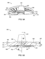
- the showerhead plate contains an inner area configured to position the plasma baffle therein and an outer area which has a plurality of holes for emitting a process gas.
- the plasma baffle contains a conical nose disposed on an upper surface to receive another process gas, a lower surface to emit the process gas and a plurality of openings configured to flow the process gas from above the upper surface into a process region.
- the openings are slots positioned at a predetermined angle to emit the process gas with a circular flow pattern.
- the plasma baffle assembly contains a plurality of slots extending from the first gas region through the assembly to provide fluid communication from the first gas region into the process region.
- the plasma baffle assembly further contains a nose cone extending from an upper surface of the plasma baffle to a lower surface of the plasma screen.
- the slots extend across the upper surface between the nose cone and an outer edge of the assembly at a tangential angle from a center portion.
- Each slot is extended through the plasma baffle assembly at a predetermined injection angle relative to the substrate receiving surface.
- the predetermined injection angle may be within a range from about 20° to about 70°, preferably, from about 30° to about 60°, and more preferably, from about 40° to about 50°, such as about 45°.
- Each slot of the plurality of slots may have a width within a range from about 0.60 mm to about 0.90 mm, preferably, from about 0.70 mm to about 0.80 mm, such as about 0.76 mm and may have a length within a range from about 10 mm to about 50 mm, preferably, from about 20 mm to about 30 mm, such as about 23 mm or more.
- the plasma baffle assembly usually contains about 10 slots or more, such as about 20 slots or more.
- the slots have a width to prohibit back diffusion of gas or to prohibit formation of a secondary plasma.
- the upper surface of the plasma baffle is directed downwardly way from the nose cone. The upper surface may angled in order receive a process gas through openings of the slots and disperse the process gas with a uniform flow rate.
- a plasma baffle assembly for receiving a process gas within a plasma-enhanced vapor deposition chamber which includes a plasma baffle plate containing an upper surface to receive a process gas and a lower surface to emit the process gas.
- the plasma baffle assembly contains a plurality of openings configured to flow the process gas from above the upper surface to below the lower surface, wherein each opening is positioned at an obscured angle or at a predetermined angle, measured from a perpendicular axis of the lower surface.
- the cooling assembly contains a plurality of passageways for the second process gas to pass into the second gas region.
- the plurality of passageways provides fluid communication from the plasma screen to the second gas region.
- the plurality of passageways contains at least about 10 channels, preferably, at least about 20 channels, and more preferably, at least about 30 channels, such as about 36 channels.
- a showerhead assembly for conducting a vapor deposition process which includes a showerhead plate having a bottom surface to substantially cover a substrate receiving surface within a process chamber, an inner region of the showerhead plate for distributing a first process gas through a plurality of slots positioned at a predetermined injection angle relative to the substrate receiving surface and an outer region of the showerhead plate for distributing a second process gas through a plurality of holes.
- An inner area on the upper surface for receiving a first process gas contains a first plurality of openings configured to flow the first process gas from above the upper surface to below the lower surface.
- An outer area on the upper surface for receiving the second process gas contains a second plurality of openings configured to flow the second process gas from above the upper surface to below the lower surface.
- a cooling assembly may be positioned above and in contact with the showerhead plate. An inner region is formed between the inner area and the cooling assembly and an outer region is formed between the outer area and the cooling assembly.
- the inner region of the showerhead plate may contain a plasma baffle.
- a cooling assembly contains a plurality of passageways for directing a second process gas into the outer region.
- Each passageway of the plurality of passageways extends into the outer region at a predetermined angle.
- the predetermined angle may prohibit back diffusion of gas or formation of a secondary plasma.
- the predetermined angle may be within a range from about 5° to about 85°, preferably, from about 10° to about 45°, and more preferably, from about 15° to about 35°.
- Each passageway of the plurality of passageways may provide an obscured flow path for the second process gas into the outer region.
- the cooling assembly may have about 36 passageways.
- a lid assembly for conducting a vapor deposition process within a process chamber which includes an insulation cap and a plasma screen.
- the insulation cap has a centralized channel configured to flow a first process gas from an upper surface to an expanded channel and an outer channel configured to flow a second process gas from an upper surface to a groove which is encircling the expanded channel.
- the plasma screen has an upper surface containing an inner area with a plurality of holes and an outer area with a plurality of slots. The insulation cap may be positioned on top of the plasma screen to form a centralized gas region with the expanded channel and a circular gas region with the groove.
- an insulating cap is positioned above the plasma screen.
- the insulating cap contains at least two gas passageways, such that a first gas passageway is positioned to direct the first process gas to an inner region of the plasma screen and a second gas passageway is positioned to direct the second process gas to an outer region of the plasma screen.
- the insulating cap contains an electrically insulating material, such as a ceramic material, a quartz material or a derivative thereof.
- a gas manifold is disposed above the insulating cap and contains at least two gas passageways.
- a first gas passageway is positioned to provide the first process gas to the insulating cap and a second gas passageway is positioned to provide the second process gas to the insulating cap.
- a first conduit and a second conduit may be coupled to the first gas passageway and are positioned to provide the first process gas a gas flow in a circular direction. The first conduit and the second conduit are independently positioned to direct gas at an inner surface of the first gas passageway.
- the gas flow usually has the circular direction with a geometry of a vortex, a helix, a spiral, a swirl, a twirl, a twist, a coil, a corkscrew, a curl, a whirlpool, or derivatives thereof.
- the first conduit and the second conduit are independently positioned at an angle from a center axis of the first gas passageway. The angle may be greater than 0°, preferably, greater than about 20°, and more preferably, greater than about 35°.
- a valve may be coupled between the first conduit and a precursor source to enable an ALD process with a pulse time of about 10 seconds or less, preferably, about 6 seconds or less, and more preferably, about 1 second or less, such as within a range from about 0.01 seconds to about 0.5 seconds.
- the lower surface may further contain an inner region and an outer region, such that the first channel is in fluid communication with the inner region and the second channel is in fluid communication with the outer region.
- the inner region contains an expanding channel.
- the expanding channel may have an inner diameter within a range from about 0.5 cm to about 7 cm, preferably, from about 0.8 cm to about 4 cm, and more preferably, from about 1 cm to about 2.5 cm. Also, the expanding channel may contain an outer diameter within a range from about 2 cm to about 15 cm, preferably, from about 3.5 cm to about 10 cm, and more preferably, from about 4 cm to about 7 cm.
- the inner area further contains a zone free of the plurality of openings and a first flow pattern of the first process gas is directional at a line-of-sight to the zone, so to be directional obscure to the plurality of openings.
- the plasma screen assembly contains an inner area for receiving the first process gas and an outer area for receiving the second process gas.
- the inner area of the plasma screen assembly contains a plurality of holes for directing the first process gas to the plasma baffle assembly. Each hole may have a diameter within a range from about 0.5 mm to about 5 mm preferably, from about 1 mm to about 3 mm, such as about 1.5 mm.
- the outer area of the plasma screen contains a plurality of slots for directing the second process gas into the second gas region.
- the slots may be parallel or substantially parallel to a substrate receiving surface or the slots may be perpendicular or substantially perpendicular to the plurality of holes within the first area of the plasma screen.
- Each slot may have a width within a range from about 0.20 mm to about 0.80 mm, preferably, from about 0.40 mm to about 0.60 mm, such as about 0.51 mm.
- the plasma screen assembly contains at least about 10 slots, preferably about 36 slots or more. Also, the plasma screen assembly is formed from an electrically insulating material, such as a ceramic material, a quartz material or a derivative thereof.
- a plasma screen assembly for receiving a process gas within a plasma-enhanced vapor deposition chamber which includes an upper surface to receive gases and a lower surface to emit the gases.
- An inner area on the upper surface for receiving a first process gas contains a first plurality of openings configured to flow the first process gas from above the upper surface to below the lower surface.
- An outer area on the upper surface for receiving the second process gas contains a second plurality of openings configured to flow the second process gas from above the upper surface to below the lower surface.
- Embodiments of the invention also provide a method for forming a material on a substrate during a thermal ALD process and a PE-ALD process.
- a method is provided which includes flowing at least one process gas through at least one conduit to form a circular gas flow pattern, exposing a substrate to the circular gas flow pattern, sequentially pulsing at least one chemical precursor into the process gas and igniting a plasma from the process gas to deposit a material on the substrate.
- the circular gas flow pattern has circular geometry of a vortex, a helix, a spiral, a swirl, a twirl, a twist, a coil, a corkscrew, a curl, a whirlpool, or derivatives thereof.
- Materials that may be deposited by the method include ruthenium, tantalum, tantalum nitride, tungsten, or tungsten nitride.
- a method for depositing a material on a substrate includes positioning a substrate on a substrate support within a process chamber containing a chamber lid assembly, flowing at least one carrier gas through at least one conduit to form a circular gas flow pattern, exposing the substrate to the circular gas flow pattern, pulsing at least one precursor into the at least one carrier gas and depositing a material containing at least one element from the at least one precursor onto the substrate.
- the chamber lid assembly may contain a showerhead assembly having an inner region and an outer region, a plasma screen disposed above the showerhead assembly and configured to direct a first process gas to the inner region and a second process gas to the outer area, a first gas region located above the inner region and between the showerhead assembly and the plasma screen and a second gas region located above the outer region.
- a method for depositing a material on a substrate includes positioning a substrate on a substrate support within a process chamber containing a gas delivery system capable of forming a gas flow in a circular direction, flowing at least one carrier gas into the process chamber to form a circular gas flow pattern and exposing the substrate to the circular gas flow pattern during a plasma-enhanced atomic layer deposition process comprising sequentially igniting a plasma and pulsing at least one precursor into the at least one carrier gas to deposit a material onto the substrate.
- a method for forming a ruthenium material on a substrate includes positioning a substrate within a plasma-enhanced process chamber containing a showerhead, a plasma baffle and a plasma screen and exposing the substrate sequentially to a pyrrolyl ruthenium precursor and a reagent during an ALD process while forming a ruthenium material on the substrate.
- the pyrrolyl ruthenium precursor contains ruthenium and at least one pyrrolyl ligand with the chemical formula of:
- R 1 , R 2 , R 3 , R 4 and R 5 are each independently selected from hydrogen or an organic group, such as methyl, ethyl, propyl, butyl, amyl, derivatives thereof or combinations thereof.
- each R 2 , R 3 , R 4 and R 5 is either a hydrogen group or a methyl group.
- each R 2 and R 5 is a methyl group or an ethyl group.
- the pyrrolyl ruthenium precursor may contain a first pyrrolyl ligand and a second pyrrolyl ligand, such that the first pyrrolyl ligand may be the same as or different than the second pyrrolyl ligand.
- the pyrrolyl ruthenium precursor may contain a first pyrrolyl ligand and a dienyl ligand.
- the pyrrolyl ruthenium precursor may be a pentadienyl pyrrolyl ruthenium precursor, a cyclopentadienyl pyrrolyl ruthenium precursor, an alkylpentadienyl pyrrolyl ruthenium precursor or an alkylcyclopentadienyl pyrrolyl ruthenium precursor. Therefore, the method provides that the pyrrolyl ruthenium precursor may be an alkyl pyrrolyl ruthenium precursor, a bis(pyrrolyl) ruthenium precursor, a dienyl pyrrolyl ruthenium precursor, or derivatives thereof.
- Some exemplary pyrrolyl ruthenium precursors include bis(tetramethylpyrrolyl) ruthenium, bis(2,5-dimethylpyrrolyl) ruthenium, bis(2,5-diethylpyrrolyl) ruthenium, bis(tetraethylpyrrolyl) ruthenium, pentadienyl tetramethylpyrrolyl ruthenium, pentadienyl 2,5-dimethylpyrrolyl ruthenium, pentadienyl tetraethylpyrrolyl ruthenium, pentadienyl 2,5-diethylpyrrolyl ruthenium, 1,3-dimethylpentadienyl pyrrolyl ruthenium, 1,3-diethylpentadienyl pyrrolyl ruthenium, methylcyclopentadienyl pyrrolyl ruthenium, ethylcyclopentadie
- a method for forming a ruthenium material on a substrate includes positioning a substrate within a plasma-enhanced process chamber containing a showerhead, a plasma baffle and a plasma screen and exposing the substrate sequentially to an active reagent and a pyrrolyl ruthenium precursor during a PE-ALD process.
- a plasma may be ignited during any time period of the PE-ALD process, preferably, the plasma is ignited while the reagent is exposed to the substrate.
- the plasma activates the reagent to form an active reagent.
- an active reagent include an ammonia plasma, a nitrogen plasma and a hydrogen plasma.
- PE-ALD process provides that the plasma is generated external from the process chamber, such as by a remote plasma generator (RPS) system.
- RPS remote plasma generator
- a preferred embodiment of the PE-ALD process provides that the plasma is generated in situ by a plasma capable process chamber utilizing a radio frequency (RF) generator.
- RF radio frequency
- a method for forming a ruthenium material on a substrate includes positioning a substrate within a plasma-enhanced process chamber containing a showerhead, a plasma baffle and a plasma screen and exposing the substrate sequentially to a reagent and a pyrrolyl ruthenium precursor during a thermal-ALD process.
- the ruthenium material may be deposited on a barrier layer (e.g., copper barrier) or dielectric material (e.g., low-k) disposed on the substrate during the various ALD processes described herein.
- the barrier layer may contain a material that includes tantalum, tantalum nitride, tantalum silicon nitride, titanium, titanium nitride, titanium silicon nitride, tungsten or tungsten nitride.
- the ruthenium material is deposited on a tantalum nitride material previously formed by an ALD process or a PVD process.
- the dielectric material may include silicon dioxide, silicon nitride, silicon oxynitride, carbon-doped silicon oxides or a SiO x C y material.
- a conductive metal may be deposited on the ruthenium material.
- the conductive material may contain copper, tungsten, aluminum, an alloy thereof or a combination thereof.
- the conductive metal may be formed as one layer during a single deposition process.
- the conductive metal may be formed as multiple layers, each deposited by an independent deposition process.
- a seed layer is deposited on the ruthenium material by an initial deposition process and a bulk layer is subsequently deposited thereon by another deposition process.
- a copper seed layer is formed by an electroless deposition process, an electroplating (ECP) process or a PVD process and a copper bulk layer is formed by an electroless deposition process, an ECP process or a CVD process.
- a tungsten seed layer is formed by an ALD process or a PVD process and a tungsten bulk layer is formed by a CVD process or a PVD process.
- FIGS. 1A-1G illustrate schematic views of a process chamber as described in an embodiment herein;
- FIGS. 2A-2B illustrate a schematic view of an isolation ring as described in an embodiment herein;
- FIGS. 3A-3B illustrate schematic views of a showerhead as described in an embodiment herein;
- FIGS. 4A-4F illustrate schematic views of a water box as described in an embodiment herein;
- FIGS. 5A-5F illustrate schematic views of plasma baffle inserts as described in embodiments herein;
- FIGS. 6A-6B illustrate schematic views of a plasma screen insert as described in an embodiment herein;
- FIGS. 7A-7C illustrate schematic views of an insulation cap insert as described in an embodiment herein;
- FIGS. 8A-8D illustrate schematic views of a gas manifold assembly as described in an embodiment herein;
- FIGS. 9A-9D illustrate schematic views of a gas flows described in an embodiment herein.
- FIGS. 10A-10C illustrate alternative schematic views of a gas flows as described in an embodiment herein.
- Embodiments of the invention provide an apparatus configured to deposit a material during a thermal atomic layer deposition (ALD) process, or preferably, during a plasma-enhanced ALD (PE-ALD) process.
- ALD thermal atomic layer deposition
- PE-ALD plasma-enhanced ALD
- Other embodiments of the invention provide processes for forming the material within the process chamber.
- a process chamber is configured to perform a PE-ALD process and has multiple components that are electrically insulated, electrically grounded or RF hot.
- a chamber body and gas manifold assembly are grounded and separated by electrically insulated components, such as an isolation ring, a plasma screen insert and an insulation cap.
- a showerhead, a plasma baffle and a water box are disposed between the electrically insulated components and are RF hot when activated by a plasma generator.
- FIGS. 1A-1G illustrate schematic views of lid assembly 100 that may be used to perform a variety of ALD processes.
- process chamber 50 may be used to form materials on substrate 8 during a thermal ALD process or a PE-ALD process.
- FIG. 1A depicts a schematic cross-sectional view of process chamber 50 that may be used to perform integrated circuit fabrication.
- Process chamber 50 contains lid assembly 100 attached to chamber body assembly 90 .
- Process region 60 for substrate processing is formed and generally situated between lid assembly 100 and chamber body assembly 90 , and more specifically, just above support surface 41 of substrate support 40 and substrate 8 and just below upper surface 62 .
- the chamber spacing between upper surface 62 and support surface 41 is within a range from about 0.50 mm to about 50.00 mm, preferably, from about 1.00 mm to about 12.00 mm, and more preferably, from about 4.00 mm to about 8.00 mm, such as 5.84 mm (0.230 in).
- the spacing may vary depending on the gases being delivered and the process conditions during a deposition process.
- Substrate support 40 contains edge ring 44 and heating element 45 ( FIGS. 1A and 1G ). Heating element 45 is embedded within substrate support 40 .
- Edge ring 44 is circumferentially disposed around substrate support 40 and over an upper portion of substrate support 40 .
- Inner edge rings 48 a , 48 b and 48 c are situated on heating element 45 and below the segment of edge ring 44 which covers the upper portion of substrate support 40 .
- Edge ring 44 may be used as a purge ring by allowing an edge purge gas to flow from substrate support 40 , through gap 47 , between inner edge rings 48 a , 48 b and 48 c , edge ring 44 and heating element 45 and over the edge of substrate 8 ( FIG. 1G ). The flow of the edge purge gas prevents reactive process gasses from diffusing into heating element 45 .
- Choke gap 61 is a circumferential gap or space formed between edge ring 44 and upper surface 62 , more specifically, between the top edge surface of edge ring 44 and lower surface 202 d of isolation ring 200 . Choke gap 61 also helps provide a more uniform pressure distribution within process region 60 by partially separating process region 60 from the non-uniform pressure distribution of interior chamber region 59 . Choke gap 61 may be varied depending on the process conditions and the required pumping efficiency. The pumping efficiency during a deposition process may be controlled by adjusting choke gap 61 . Choke gap 61 is increased by lowering substrate support 40 or decreased by raising substrate support 40 .
- the pumping conductance from the pumping port 38 in the lower portion of process chamber 50 to the center of channel 820 is modified by changing the distance of choke gap 61 to control the thickness and the uniformity of a film during deposition processes described herein.
- the spacing of upper choke gap 61 is within a range from about 0.50 mm to about 50.00 mm, preferably, from about 1.00 mm to about 5.00 mm, and more preferably, from about 2.5 mm to about 4 mm, such as 3.30 mm (0.130 in).
- the pressure differentials of the pumping conductance may be controlled in order to reduce or eliminate the formation of secondary plasmas. Since the generation and sustainability of a plasma is ion concentration dependent, the pressure within a particular region may be reduced to minimize the ion concentration. Therefore, a secondary plasma may be avoided within a desired region of the process chamber.
- process chamber 50 is configured to conduct a PE-ALD process. Therefore, various regions and components throughout process chamber 50 are electrically insulated, electrically grounded or RF hot.
- chamber body 80 and gas manifold assembly 800 are grounded and separated by electrically insulated isolation ring 200 , plasma screen insert 600 and insulation cap 700 .
- Process chamber 50 also contains insulator ring liner 82 , chamber liner 84 and other insulation liners to minimize or completely eliminate any line-of-sight between upper surface 62 and the various surfaces of chamber body assembly 90 .
- the insulation liners help minimize or eliminate plasma erosion of the metallic surfaces of chamber body assembly 90 . Therefore, substrate support 40 and a wafer contained thereon are a grounded path from RF powered showerhead 300 while generating a plasma.
- process region 60 is isolated from interior chamber region 59 , a reactant gas or purge gas needs only adequately fill process region 60 to ensure sufficient exposure of substrate 8 to the reactant gas or purge gas.
- process chambers are required to provide a combined flow of reactants simultaneously and uniformly to the entire substrate surface in order to ensure that the co-reaction of the reactants occurs uniformly across the surface of substrate 8 .
- process chamber 50 is used to sequentially expose substrate 8 to chemical reactants, such as a gas or a plasma, that adsorb or react as thin layers onto the surface of substrate 8 .
- an ALD process does not require a flow of a reactant to simultaneously reach the surface of substrate 8 . Instead, a flow of a reactant needs to be provided in an amount which is sufficient to adsorb a thin layer of the reactant on the surface of substrate 8 or in an amount which is sufficient to react with an adsorbed layer on the surface of substrate 8 .
- process region 60 may comprise a smaller volume when compared to the inner volume of a conventional CVD chamber, a smaller amount of gas is required to fill process region 60 for a particular process in an ALD sequence.
- interior chamber region may have a volume of about 20 L
- process region 60 is separated from interior chamber region 59 to have a smaller volume, such as about 3 L or less, preferably, about 2 L or less, and more preferably, about 1 L or less.
- the volume of process region 60 is about 1,000 cm 3 or less, preferably, about 500 cm 3 or less, and more preferably, about 200 cm 3 or less.
- the volume of process region 60 is about 3,000 cm 3 or less, preferably, about 1,500 cm 3 or less, and more preferably, about 1,000 or less, such as about 800 cm 3 or less.
- process region 60 has a volume of about 770 cm 3 or less.
- substrate support 40 may be raised or lowered to adjust the volume of process region 60 .
- substrate support 40 may be raised to form process region 60 having a volume of about 770 cm 3 or less.
- the smaller volume of process region 60 requires less gas (e.g., process gas, carrier gas or purge gas) to be flowed into process chamber 50 during a process. Therefore, the throughput of process chamber 50 is greater since less time is needed to provide and remove gases and the operation cost is reduced since the waste of chemical precursors and other gases may be minimized due to the smaller amount of the gases.
- FIG. 1B further illustrates an exploded view of lid assembly 100 and components thereof.
- Lid support 103 having lower surface 102 and upper surface 104 may be formed from a variety of materials including a metal.
- lid support 103 is formed from a metal, such as aluminum, steel, stainless steel (e.g., iron-chromium alloys optionally containing nickel), iron, nickel, chromium, an alloy thereof or combinations thereof.
- Lid assembly 100 may be attached to chamber body assembly 90 by hinges (not shown). Alignment slots 101 on lid support 103 are positioned to be aligned with a post (not shown) attached to chamber body assembly 90 , once lid assembly is in a closed position.
- Lid support 103 also contains support bracket 110 and handle assembly 107 mounted on upper surface 104 .
- Handle assembly 107 may contain thermal isolator 108 between handle 106 positioned on upper surface 104 .
- lid assembly 100 has opening 120 with ledge surface 122 and wall surface 124 .
- Multiple holes and openings, such as ports 116 , 117 and 118 may also pass through lid support 103 and may provide a passageway for conduit, tubing, hosing, fasteners, instruments and other devices.
- Lid support 103 further contains holes that may not pass through. For example, holes 119 may be threaded and used to receive a fastener, such as a screw or a bolt.
- Lid assembly 100 further contains isolation ring 200 , showerhead 300 , water box 400 , plasma baffle insert 500 , plasma screen insert 600 , insulation cap 700 and gas manifold assembly 800 .
- Each component i.e., isolation ring 200 , showerhead 300 , water box 400 , plasma baffle insert 500 , plasma screen insert 600 , insulation cap 700 or gas manifold assembly 800
- lid assembly 100 may be scaled to process a substrate of varying size, such as a wafer with a 150 mm diameter, a 200 mm diameter, a 300 mm diameter or larger.
- each component may be positioned and secured on lid support 103 by clips 780 .
- Clip 780 latches over upper surface 404 of water box 400 and is secured by a fastener placed through holes 119 ( FIGS. 1A-1G ).
- clip 780 contains metal clip segment 784 disposed on insulator segment 782 .
- Insulator segment 782 may be formed from an electrically insulating material, a thermally insulating material or a combination thereof. Insulator segments 782 provide electrical and thermal isolation between upper surface 404 and lid support 103 while clips 780 secure the various components of lid assembly 100 .
- Axis 10 pass through the center of lid assembly 100 including, once aligned, opening 120 of lid support 103 and opening 220 of isolation ring 200 , opening 320 of showerhead 300 , opening 420 of water box 400 , conical nose 520 of plasma baffle insert 500 , center portion 601 of plasma screen insert 600 , channel 720 of insulation cap 700 and channel 820 of gas manifold assembly 800 .
- FIG. 1C depicts a view from underneath lid assembly 100 , down axis 10 , to illustrate upper surface 62 and lower surface 102 of lid support 103 .
- Upper surface 62 of process region 60 is formed collectively of lower surfaces 202 d and 205 d of isolation ring 200 , lower surface 302 c of showerhead 300 and lower surface 502 of plasma baffle insert 500 .
- Substrate 8 is positioned below upper surface 62 within process region 60 and exposed to process gases during a deposition process. In one embodiment, the substrate is sequentially exposed to at least two process gases (e.g., gas or plasma) during an ALD process. In one example of an ALD process, substrate 8 is exposed to a first process gas coming from slots 510 of plasma baffle insert 500 and to a second process gas coming from holes 310 of showerhead 300 .
- process gases e.g., gas or plasma
- a view along axis 10 further illustrates that although opening 508 of slot 510 is visible on lower surface 502 , the other end of slot 510 (e.g., opening 506 on upper surface 503 , FIG. 5C ) is not visible.
- This obscured view down axis 10 is due to the angle of slots 510 (angle ⁇ 1 in FIG. 5B ) that depict a pathway between process region 60 and gas region 640 above plasma baffle insert 500 does not have a line-of-sight.
- the obscured pathway has many advantages over a non-obscured pathway having a line-of-sight between process region 60 and gas region 640 including a reduction or absence of a secondary plasma within or above plasma baffle insert 500 .
- Line-of-sight refers to a straight path or a substantially straight path between two points.
- the straight path or the substantially straight path may provide an unobstructed pathway or an unobscured pathway for a gas or a plasma to flow between at least two points.
- an obstructed pathway or an obscured pathway prohibits or substantially reduces the passage of a plasma while permitting the passage of a gas. Therefore, a line-of-sight pathway usually permits the passage of a gas or a plasma, while a pathway not have a line of sight between two points prohibits or substantially reduces the passage of a plasma and permits the passage of a gas.
- a portion of upper surface 62 may be roughened (e.g., machined) to produce more surface area across upper surface 62 .
- the increased surface area of upper surface 62 may increase adhesion of accumulated material during a deposition process, while decreasing contaminants due to the flaking of the accumulated material.
- the mean roughness (R a ) of each lower surface 302 c and lower surface 502 independently may be at least about 15 microinch (about 0.38 ⁇ m), preferably, about 100 microinch (about 2.54 ⁇ m), and more preferably, about 200 microinch (about 5.08 ⁇ m) or higher.
- Lower surface 102 of lid support 103 may also be roughened to have a roughness of at least about 15 microinch (about 0.38 ⁇ m), preferably, at least about 50 microinch (about 1.27 ⁇ m), for example, about 54 microinch (about 1.37 ⁇ m).
- FIGS. 1B and 1D further illustrates gas manifold assembly 800 containing conduit assembly 840 , manifold cap assembly 850 and gas conduit assembly 830 .
- Manifold cap assembly 850 may have viewing window assembly 826 for observing ignited plasma ( FIG. 1A ).
- manifold cap assembly 850 may contain surface 825 which lacks a viewing window ( FIG. 1D ).
- Gas conduit assembly 830 may be connected to and in fluid communication with port 117 at flange 834 while extended to be connected to and in fluid communication with gas inlet 813 on manifold block 806 ( FIGS. 1D and 8D ).
- plasma generator system 92 is attached to lid assembly 100 by RF strap 88 ( FIG. 1D ).
- a portion of plasma generator system 92 namely RF stinger 94 and insulator 95 a , protrudes through port 116 on lid support 103 and couples to showerhead 300 and water box 400 .
- Insulator 95 a maintains RF stinger 94 electrically isolated from lid support 103 while RF strap electrically connects RF stinger 94 to region 950 containing contacts 350 and 450 on showerhead 300 and water box 400 .
- RF stinger 94 is a conductive material, such as a metal rod or electrode, which may contain copper, brass, stainless steel, steel, aluminum, iron, nickel, chromium, alloys thereof, other conductive materials or combinations thereof.
- Plasma generator system 92 further contains plasma generator 97 that may be mounted under chamber body 80 ( FIG. 1E ). Insulator 95 b may be placed between plasma generator 97 and chamber body 80 to electrically isolate plasma generator 97 . Match 96 may protrude through insulator 95 b and be in electrical contact with chamber body 80 . Plasma generator 97 further contains connector 98 . In one example, connector 98 is an RF coaxial cable connector, such as a type N connector. Plasma generator system 92 may be operated by plasma generator controller 22 connected to signal bus system 30 . In one example, process conditions of plasma generator system 92 may be set to have a chamber impedance of about 4 ohms with about 9 amperes at about 300 watts.
- a plasma system and a process chamber that may be used in combination with lid assembly 100 or may be used as plasma generator system 92 and chamber body assembly 90 is the TXZ® CVD, chamber available from Applied Materials, Inc., located in Santa Clara, Calif. Further disclosure of plasma systems and process chambers is described in commonly assigned U.S. Pat. Nos. 5,846,332, 6,079,356, and 6,106,625, which are incorporated herein by reference in their entirety, to provide further disclosure for a plasma generator, a plasma chamber, a vapor deposition chamber, a substrate pedestal and chamber liners.
- Chamber body assembly 90 of process chamber 50 contains insulator ring liner 82 that is used to reduce plasma exposure to chamber body 80 and helps ensure that plasma is confined within process region 60 ( FIG. 1F ). Also, chamber body assembly 90 generally houses substrate support 40 attached to post 42 within interior chamber region 59 . Substrate support 40 is movable in a vertical direction inside process chamber 50 using support controller 20 . In one embodiment, substrate support 40 is rotatable. Process region 60 is situated above substrate support 40 and below lid assembly 100 , preferably, at least below showerhead 300 , plasma baffle insert 500 and a portion of isolation ring 200 .
- substrate 8 may be heated to some desired temperature prior to or during a pretreatment step, a deposition step, post-treatment step or other process step used during the fabrication process.
- substrate support 40 may be heated using embedded heating element 45 .
- Substrate support 40 may be resistively heated by applying an electric current from AC power supply to heating element 45 .
- Substrate 8 is, in turn, heated by substrate support 40 .
- substrate support 40 may be heated using radiant heaters such as, for example, lamps (not shown).
- Temperature sensor 46 such as a thermocouple, is also embedded in substrate support 40 to monitor the temperature of substrate support 40 in a conventional manner. The measured temperature is used in a feedback loop to control AC power supply for heating element 45 , such that the temperature of substrate 8 may be maintained or controlled at a desired temperature which is suitable for the particular process application.
- Substrate lift pins (not shown) may also be embedded in substrate support 40 and are used to raise substrate 8 from support surface 41 .
- Vacuum pumping system 36 is used to evacuate and to maintain the pressure inside process chamber 50 ( FIG. 1F ). Vacuum pumping system 36 may be connected to process chamber 50 by pumping port 38 and valve 37 . Gas manifold assembly 800 , through which process gases are introduced into process chamber 50 , is located above substrate support 40 . Gas manifold assembly 800 may be connected to a gas panel, which controls and supplies various process gases to process chamber 50 .
- Gas sources 70 a , 70 b , 70 c , 70 d , and 70 e provide precursor gas, carrier gas or purge gas to process chamber 50 through conduit system 34 .
- Gas sources 70 a , 70 b , 70 c , 70 d and 70 e may be directly or indirectly connected to a chemical supply or a gas supply.
- the chemical or gas supplies include a tank, an ampoule, a bubbler, a vaporizer or another container used to store, transfer or form a chemical precursor.
- the chemical or gas supply may also be from an in-house source.
- Gas manifold assembly 800 allows process gases to be introduced into process chamber 50 and may optionally be heated to prevent condensation of any gases within the conduits or lines of gas manifold assembly 800 .
- Each valve assembly 72 a , 72 b , 72 c , 72 d and 72 e may comprise a diaphragm and a valve seat.
- the diaphragm may be biased open or closed and may be actuated closed or open respectively.
- the diaphragms may be pneumatically actuated or may be electrically actuated. Examples of pneumatically actuated valves are available from Fujikin and Veriflow and examples of electrically actuated valves are available from Fujikin.
- Control unit 51 may be coupled to valve assemblies 72 a , 72 b , 72 c , 72 d and 72 e to control actuation of the diaphragms of the valves.
- Pneumatically actuated valves may provide pulses of gases in time periods as low as about 0.020 seconds. Electrically actuated valves may provide pulses of gases in time periods as low as about 0.005 seconds. Generally pneumatically and electrically actuated valves may provide pulses of gases in time periods as high as about 3 seconds. Although higher time period for gas pulsing is possible, a typical ALD process utilizes ALD valves to generate pulses of gas while being opened for an interval of about 5 seconds or less, preferably about 3 seconds or less, and more preferably about 2 seconds or less.
- an ALD valve pulses for an interval in a range from about 0.005 seconds to about 3 seconds, preferably from about 0.02 seconds to about 2 seconds and more preferably from about 0.05 seconds to about 1 second.
- An electrically actuated valve typically requires the use of a driver coupled between the valve and control unit 51 .
- each valve assemblies 72 a , 72 b , 72 c , 72 d and 72 e may contain a mass flow controller (MFC) to control gas dispersion, gas flow rates and other attributes to an ALD pulse sequence.
- MFC mass flow controller
- a precursor or a gas delivery system within an ALD apparatus is used to store and dispense chemical precursors, carrier gases, purge gases or combinations thereof.
- the delivery system may contain valves (e.g., ALD valves or MFCs), conduits, reservoirs, ampoules and bubblers, heater and/or control unit systems, which may be used with process chamber 50 or lid assembly 100 and coupled in fluid communication with gas manifold 800 or conduit system 34 .
- a delivery system may contain gas sources 70 a - 70 e and valve assemblies 72 a , 72 b , 72 c , 72 d , and 72 e coupled to control unit 51 . Delivery systems configured for an ALD process system are described in commonly assigned U.S. Ser. No.
- Control unit 51 such as a programmed personal computer, work station computer, or the like, may be coupled to process chamber 50 to control processing conditions.
- control unit 51 may be configured to control flow of various process gases and purge gases from gas sources 70 a - 70 e through valve assemblies 72 a - 72 e during different stages of a substrate process sequence.
- control unit 51 comprises central processing unit (CPU) 52 , support circuitry 54 , and memory 56 containing associated control software 58 .
- CPU central processing unit
- Software routines may be stored in memory 56 or executed by a remotely located source (e.g., computer or server).
- the software routines are executed to initiate process recipes or sequences.
- the software routines when executed, transform the general purpose computer into a specific process computer that controls the chamber operation during a chamber process.
- software routines may be used to precisely control the activation of gas sources 70 a - 70 e through valve assemblies 72 a - 72 e during the execution of process sequences according to the embodiments described herein.
- the software routines may be performed in the hardware, as an application specific integrated circuit or other type of hardware implementation or a combination of software or hardware.
- Control unit 51 may be one of any form of general purpose computer processor that can be used in an industrial setting for controlling various chambers and sub-processors.
- CPU 52 may use any suitable memory 56 , such as random access memory, read only memory, floppy disk drive, compact disc drive, hard disk or any other form of digital storage, local or remote.
- Various support circuits may be coupled to the CPU 52 for supporting process chamber 50 .
- Control unit 51 may be coupled to another controller that is located adjacent individual chamber components, such as programmable logic controllers of valve assemblies 72 a - 72 e . Bi-directional communications between control unit 51 and various other components of process chamber 50 are handled through numerous signal cables collectively referred to as signal buses 30 , some of which are illustrated in FIG. 1F .
- control unit 51 may be configured to be responsible for automated control of other activities used during a fabrication process.
- Control unit 51 is connected to plasma generator controller 22 , vacuum pumping system 36 and support controller, including temperature monitoring and control and control of lift pins (not shown).
- Isolation ring 200 contains opening 220 ( FIGS. 2A-2B ) and may be positioned between showerhead 300 and lid support 103 ( FIGS. 1A-1B ). Isolation ring 200 contains upper surface 204 to support showerhead 300 . Opening 220 may be aligned with opening 120 such that axis 10 passes through each center. Isolation ring contains inner surfaces 205 a , 205 b , 205 c and 205 d that taper inward towards axis 10 .
- Isolation ring 200 further contains lower surfaces 202 a , 202 b , 202 c and 202 d .
- Lower surface 202 a may be used to contact ledge surface 122 of lid support 103 while supporting isolation ring 200 .
- Lower surfaces 202 d and 205 d forms process region 60 while contributing to upper surface 62 therein ( FIG. 1C ).
- the portion of upper surface 62 contributed by lower surface 202 d forms an outer ring seal between process region 60 and interior chamber region 59 .
- Isolation ring 200 may be formed from an electrically insulating material that is plasma resistant or chemical resistant against the process reagents.
- Isolation ring 200 may also contain a thermally insulating material. Materials useful to construct isolation ring 200 include ceramic, quartz, fused quartz, sapphire, pyrolytic boron nitrite (PBN) material, glass, plastic, derivatives thereof, or combinations thereof.
- PBN pyrolytic boron nitrite
- showerhead 300 contains opening 320 ( FIGS. 3A-3B ) and may be positioned between isolation ring 200 and water box 400 ( FIG. 1A-1B ).
- showerhead 300 contains upper surfaces 303 , 304 , and 306 , where upper surfaces 304 and 306 may be used to support water box 400 .
- Wall surfaces 305 a and 305 b are disposed between upper surfaces 303 , 304 and 306 .
- showerhead 300 further contains lower surfaces 302 a , 302 b , and 302 c .
- Lower surface 302 a may be used to contact upper surface 204 of isolation ring 200 while supporting showerhead 300 .
- Lower surface 302 c also forms process region 60 while contributing to upper surface 62 therein ( FIG. 1C ).
- showerhead 300 may be formed from a variety of materials including a metal or another electrically conductive material.
- showerhead 300 is formed from a metal, such as aluminum, steel, stainless steel, iron, nickel, chromium, an alloy thereof
- Opening 320 passes through showerhead 300 and may be aligned with openings 120 and 220 such that axis 10 passes through each center ( FIG. 1B ). Also, opening 320 passes through ring assembly 330 .
- Ring assembly 330 is positioned in the center of showerhead 300 and may be used to house plasma baffle insert 500 .
- Ring assembly 330 contains ring 328 disposed above the surface of upper surface 303 .
- Ledge 332 protrudes inwardly from ring 328 towards axis 10 and is used to support plasma baffle insert 500 thereon.
- Ledge 322 protrudes outwardly from ring 328 away from axis 10 and is used to support water box 400 in conjunction with upper surfaces 304 and 306 .
- Upper surface 324 of ring 328 is used to support plasma screen insert 600 .
- Upper surface 303 of showerhead 300 receives a process gas for distributing into process region 60 through holes 310 .
- Holes 310 pass through showerhead 300 from upper surface 303 to lower surface 302 c and provide fluid communication therethrough.
- Holes 310 in showerhead 300 may have a diameter within a range from about 0.10 mm to about 1.00 mm, preferably, from about 0.20 mm to about 0.80 mm, and more preferably, from about 0.40 mm to about 0.60 mm.
- showerhead 300 may have at least about 100 holes, preferably, about 1,000 holes, and more preferably, about 1,500 holes or more.
- showerhead 300 may have as many as 6,000 holes or 10,000 holes depending on size of the holes 310 , the distribution pattern of the holes 310 , size of substrate and desired exposure rate.
- Holes 310 may have a varying or consistent geometry from hole to hole.
- showerhead 300 is constructed from metal (e.g., aluminum or stainless steel) and has 1,500 holes that are formed with a diameter of 0.50
- showerhead 300 contains opening 320 ( FIG. 3 ) and may be positioned between isolation ring 200 and water box 400 ( FIG. 1A-1B ).
- showerhead 300 contains upper surfaces 303 , 304 and 306 , where upper surfaces 304 and 306 may be used to support water box 400 .
- Wall surfaces 305 a and 305 b are disposed between upper surfaces 303 , 304 and 306 .
- showerhead 300 further contains lower surfaces 302 a , 302 b and 302 c .
- Lower surface 302 a may be used to contact upper surface 204 of isolation ring 200 while supporting showerhead 300 .
- Lower surface 302 c also forms process region 60 while contributing upper surface 62 therein ( FIG. 1C ).
- showerhead 300 may be formed from a variety of materials including a metal or another electrically conductive material.
- showerhead 300 is formed from a metal, such as aluminum, steel, stainless steel, iron, nickel, chromium, alloys thereof or combinations thereof.
- a plurality of holes 310 are formed through showerhead 300 , so that upper surface 303 is in fluid communication to lower surface 302 c .
- Holes 310 may have a variety of sizes and be contained across upper surface 303 and lower surface 302 c in multiple patterns.
- Each hole of the plurality of holes 310 may have a diameter within a range from about 0.10 mm to about 1.00 mm, preferably, from about 0.20 mm to about 0.80 mm, and more preferably, from about 0.40 mm to about 0.60 mm, such as about 0.51 mm (0.020 in).
- showerhead 300 has at least about 100 holes, preferably, about 1,000 holes, and more preferably, about 1,500 holes or more.
- showerhead 300 may have as many as 6,000 holes or 10,000 holes depending on size of holes 310 , the pattern of the holes, size of substrate and desired exposure rate.
- showerhead 300 is constructed from a metal (e.g., aluminum or stainless steel) and has 1,500 holes that are formed with a diameter of about 0.50 mm.
- Water box 400 containing opening 420 ( FIGS. 4A-4B ), may be positioned on top of showerhead 300 and used to regulate the temperature by removing heat from lid assembly 100 ( FIG. 1A-1B ).
- Opening 420 contains ledge surfaces 414 a and 414 b and inner surfaces 416 a , 416 b and 416 c .
- a plurality of passageways 440 radial extend from inner surface 416 b inwardly through water box 400 to lower surface 402 c .
- Opening 420 is adapted to receive plasma baffle insert 500 , plasma screen insert 600 , insulation cap 700 .
- Insulation cap 700 may be positioned on ledge surface 414 a .
- Water box 400 may be formed from a variety of materials including a metal.
- water box 400 is formed from aluminum, steel, stainless steel, iron, nickel, chromium, an alloy thereof, another metal, or combinations thereof.
- Lower surfaces 402 a and 402 b of water box 400 rests on upper surfaces 304 and 306 of showerhead 300 .
- Water box 400 also contains upper surface 403 surrounded by inner surface 405 which has upper surface 404 .
- Water box 400 helps remove heat from lid assembly 100 , especially from showerhead 300 .
- Upper surface 403 contains inlet 410 and outlet 412 that are in fluid communication with passageway 430 .
- a fluid at an initial temperature is administered into water box 400 through inlet 410 .
- the fluid absorbs heat while traveling along passageway 430 .
- the fluid at a higher temperature is removed from water box 400 through outlet 412 .
- the fluid may be in liquid, gas or supercritical state and is capable of adsorbing and dissipating heat in a timely manner.
- Liquids that may be used in water box 400 include water, oil, alcohols, glycols, glycol ethers, other organic solvents, supercritical fluids (e.g., CO 2 ) derivatives thereof or mixtures thereof.
- Gases may include nitrogen, argon, air, hydrofluorocarbons (HFCs), or combinations thereof.
- water box 400 is supplied with water or a water/alcohol mixture.
- Inlet 410 may be adapted to receive nozzle 411 connected to line 425 (e.g., hose) in fluid communication with a fluid source.
- outlet 412 may be adapted to receive nozzle 413 connected to line 427 in fluid communication with a fluid return.
- the fluid source and fluid return may be an in-house cooling system or an independent cooling system.
- Lines 425 and 427 are connected to source nozzle 421 and return nozzle 423 held in positioned on lid support 103 by support bracket 110 .
- Lines 425 and 427 may be a tube, a hose, a conduit or a line.
- the fluid may be administered into water box 400 at a temperature within a range from about ⁇ 20° C. to about 40° C., preferably, from about 0° C. to about 20° C.
- the temperature, flow rate, and fluid composition may be adjusted accordingly to remove the appropriate amount of heat from lid assembly 100 including showerhead 300 while maintaining water box 400 at a predetermined temperature.
- Water box 400 may be maintained at a predetermined temperature within a range from about 0° C. to about 100° C., preferably, from about 18° C. to about 65° C., and more preferably, from about 20° C. to about 50° C.
- FIGS. 4C-4F illustrate passageways 430 c , 430 d , 430 e and 430 f to provide several different geometries that may be used to replace passageway 430 .
- Passageways 430 c - 430 f may include a partial loop 432 c ( FIG. 4C ), a single loop 432 d ( FIG. 4D ), multiple loops 432 e ( FIG. 4E ) or contain branches or spurs 432 f around opening 420 ( FIG. 4F ).
- Gas region 540 is above upper surface 303 of showerhead 300 and below the lower surface 402 c of water box 400 .
- Passageways 440 extend from inner surface 416 b , pass through water box 400 and into gas region 540 .
- Inner surface 416 b may be inwardly concaved such to form gas region 441 that is situated between inner surface 416 b and plasma screen insert 600 and insulation cap 700 ( FIG. 7C ).
- Gas region 441 encompasses plasma screen insert 600 to maintain fluid communication with slots 614 .
- Passageways 440 provide fluid communication between gas regions 441 and 540 .
- Water box 400 contains numerous passageways 440 .
- water box 400 may contain at least about 10 passageways, preferably, at least about 24 passageways, and more preferably, at least about 36 passageways or more.
- FIGS. 5A-5F illustrate schematic views of plasma baffle insert 500 that may be included as a portion of lid assembly 100 as described in several embodiments.
- Plasma baffle insert 500 is configured to receive a process gas from gas region 640 and distribute or inject the process gas into process region 60 .
- plasma baffle insert 500 is configured to distribute the process gas at a predetermined angle.
- Upper surface 503 contains slots 510 extending through plasma baffle insert 500 to lower surface 502 for distributing the process gas into process region 60 .
- Plasma baffle insert 500 is illustrated containing conical nose 520 extending from upper surface 503 to nose surface 522 ( FIG. 5A ).
- Nose surface 522 may have a variety of geometries, such as flat ( FIG. 5B ) or conical nose 520 may extend to a point (not illustrated).
- nose surface 522 is substantially, horizontally flat for contacting plasma screen insert 600 .
- Conical nose 520 may extend into gas region 640 , which is a region formed above plasma baffle insert 500 , below plasma screen insert 600 and within ring assembly 330 . Conical nose 520 occupies a predetermined volume within gas region 640 .
- a less amount of process gas is required to fill gas region 640 during a deposition process if conical nose 520 occupies a larger volume. Therefore, a quicker ALD cycle is realized since a reduced amount of process gas is more quickly administered and removed from gas region 640 during each half cycle of an ALD process.
- Plasma baffle insert 500 contains lower rim 512 having lower surface 502 and upper rim 514 having upper surface 505 and lower surface 504 . Lower rim 512 and upper rim 514 are separated by gap 513 .
- a gasket may be placed within gap 513 to provide more conductivity or a better seal.
- a gasket may include an o-ring or sealant.
- the gasket is a RF gasket and contains a conductive material, such as a metal cable or a conductively doped-polymeric material.
- a RF gasket such as a twisted stainless steel cable, is placed along gap 513 to provide a more conductive contact with showerhead 300 .
- Plasma baffle insert 500 may be positioned within opening 320 of showerhead 300 so that lower surface 504 of upper rim 514 rests on ledge 332 of showerhead 300 ( FIG. 1A-1B ). Plasma baffle insert 500 is also circumferentially surrounded by ring assembly 330 within opening 320 . Plasma baffle insert 500 may be formed from aluminum, steel, stainless steel, iron, nickel, chromium, other metals, alloys thereof or combinations thereof.
- Plasma baffle insert 500 contains a plurality of slots 510 , such that openings 508 of upper surface 503 is in fluid communication to openings 506 of lower surface 502 ( FIGS. 1C and 5C ). Slots 510 provide access for a process gas to flow from gas region 640 and into process region 60 at a predetermined angle. Ideally, slots 510 direct the process gas to contact substrate 8 or support surface 41 at an injection angle ⁇ 1 measured between axis 10 and line 532 . Axis 10 extends perpendicular through lower surface 502 while line 532 extends along the plane of slots 510 . Therefore, slots 510 contained within plasma baffle insert 500 are positioned at injection angle ⁇ 1 to direct a process gas having a flow pattern at injection angle ⁇ 1 , as depicted in FIGS. 5 C and 9 C- 9 D.
- plasma baffle insert 500 may contain trough 501 or a plurality of holes 530 to assist in moving process gases from upper surface 503 .
- plasma baffle insert 500 may contain trough 501 around an outside perimeter of slots 510 , as depicted in FIGS. 5A-5C .
- slots 510 may extend into trough 501 (not shown).
- plasma baffle insert 500 may contain holes 530 around an outside perimeter of conical nose 520 , as depicted in FIGS. 5D-5F .
- Each hole 530 extends from upper surface 503 to lower surface 502 along axial line 538 .
- each hole 530 has a constant diameter along axis line 538 .
- each hole 530 contains upper passageway 526 a and lower passageway 526 b separated by choke 528 .
- the diameter of upper passageway 526 a is usually larger than the diameter of lower passageway 526 b.
- a process gas with a flow pattern parallel or perpendicular to support surface 41 may unevenly accumulate a chemical precursor across the surface of substrate 8 .
- substrate 8 may exposed to the process gas at a predetermined angle of less than about 90°, but more than about 0°, to ensure an even exposure of the process gas.
- injection angle ⁇ 1 of slots 510 may be at an angle within a range from about 20° to about 70°, preferably, from about 30° to about 60°, and more preferably, from about 40° to about 50°, such as about 45°.
- the process gas may have a circular pathway inherited from the injection angle ⁇ 1 of slots 510 .
- the circular pathway usually has a vortex geometry, a helix geometry, a spiral geometry, a swirl geometry, a twirl geometry, a twist geometry, a coil geometry, a corkscrew geometry, a curl geometry, a whirlpool geometry, or derivatives thereof.
- Holes 530 contained within plasma baffle insert 500 may be positioned at injection angle ⁇ 5 to direct a process gas having flow pattern 912 at injection angle ⁇ 5 , as depicted in FIGS. 5 F and 9 C- 9 D.
- injection angle ⁇ 5 of holes 530 may be at an angle within a range from about 0° to about 60°, preferably, from about 15° to about 50°, and more preferably, from about 30° to about 40°, such as about 35°.
- Flow pattern 912 of the process gas may have a conical pathway inherited from the injection angle ⁇ 5 of holes 530 .
- a secondary plasma or back diffusion of gasses within or above the plasma baffle insert 500 may be avoided by limiting the width and length of slots 510 and holes 530 . Also, a secondary plasma within or above the plasma baffle insert 500 may be avoided or limited by positioning slots 510 at a predetermined injection angle ⁇ 1 , such that there is not a line-of-sight through plasma baffle insert 500 , along axis 10 , from support surface 41 to gas region 640 ( FIG. 1C ).
- the secondary plasma within or above the plasma baffle insert 500 may also be avoided or limited by positioning holes 530 at a predetermined injection angle ⁇ 5 , such that there is not a line-of-sight through plasma baffle insert 500 , along axial line 538 , from support surface 41 to gas region 640 ( FIG. 1F ).
- slots 510 and openings 506 and 508 may have a width within a range from about 0.50 mm to about 1.00 mm, preferably, from about 0.60 mm to about 0.90 mm, and more preferably, from about 0.70 mm to about 0.80 mm, such as about 0.76 mm (0.030 in).
- slots 510 and openings 506 and 508 may have a length within a range from about 3 mm to about 60 mm, preferably, from about 10 mm to about 50 mm, and more preferably, from about 20 mm to about 30 mm, such as about 21.6 mm (0.850 in).
- Plasma baffle insert 500 may have at least about 10 slots, preferably, about 15 slots, and more preferably, about 20 slots or more.
- plasma baffle insert 500 is constructed from metal (e.g., aluminum or stainless steel) and has 20 slots that are about 0 . 76 mm wide and about 21.6 mm long.
- each hole 530 may have a diameter within a range from about 0.13 mm (0.005 in) to about 2.54 mm (0.100 in), preferably, from about 0.26 mm (0.010 in) to about 2.29 mm (0.090 in), and more preferably, from about 0.51 mm (0.020 in) to about 1.90 mm (0.075 in).
- each hole 530 may contain upper passageway 526 a having a diameter within a range from about 1.27 mm (0.050 in) to about 2.29 mm (0.090 in), preferably, from about 1.52 mm (0.060 in) to about 2.03 mm (0.080 in), such as about 1.78 mm (0.070 in).
- each hole 530 may contain lower passageway 526 b having a diameter within a range from about 0.38 mm (0.015 in) to about 1.27 mm (0.050 in), preferably, from about 0.64 mm (0.025 in) to about 1.02 mm (0.040 in), such as about 0.81 mm (0.032 in).
- each hole 530 contains upper passageway 526 a having a diameter within a range from about 1.5 mm to about 2 mm and lower passageway 526 b having a diameter within a range from about 0.6 mm to about 1 mm.
- Plasma baffle insert 500 may have no holes or a plurality of holes 530 , such as about 4 holes, preferably, about 8 holes, and more preferably, about 16 holes or more.
- plasma baffle insert 500 is constructed from metal (e.g., aluminum or stainless steel) and has 8 holes.
- upper surface 503 of plasma baffle insert 500 is sloped from conical nose 520 towards upper rim 514 .
- the process gas is directed from holes 612 towards conical nose 520 and down upper surface 503 towards upper rim 514 .
- plasma baffle insert 500 is formed with upper surface 503 sloped downwardly from conical nose 520 to provide greater mechanical strength and to control varying conductance and flow rates during a process.
- Upper surface 503 may have a slope with an angle ⁇ 2 measured between lines 535 and 537 . Line 535 extends along the plane of upper surface 503 and line 537 is perpendicular or substantially perpendicular to axis 10 ( FIG. 5B ).
- Upper surface 503 is configured to receive a process gas along various portions of openings 506 relative to angle ⁇ 2 . Therefore, angle ⁇ 2 may be at a predetermined angle in order to eject the process gas from openings 508 of slots 510 with a consistent flow rate along the length of openings 506 . In one embodiment, upper surface 503 may be sloped at an angle ⁇ 2 within a range from about 0° to about 45°, preferably, from about 5° to about 30°, and more preferably, from about 10° to about 20°, such as about 15°.
- upper surface 503 may be sloped at an angle ⁇ 2 within a range from about 0° to about 45°, preferably, from about 2° to about 20°, and more preferably, from about 3° to about 10°, such as about 5°.
- Openings 506 and 508 may be disposed around conical nose 520 at angle ⁇ 3 , measured between line 531 and radial line 533 .
- Line 531 extends along the length of opening 506 and radial line 533 extends perpendicular from axis 10 .
- Line 531 may also extend along the length of opening 508 (not shown).
- openings 506 and 508 may be disposed around conical nose 520 and are tangential or substantially tangential to dashed circle 539 at angle ⁇ 3 .
- line 531 extending along the length of opening 506 , may intersect a point on dashed circle 539 and is tangent or substantially tangent to dashed circle 539 at angle ⁇ 3 .
- Dashed circle 539 may have a radius of a length within a range from about 0.5 mm to about 5 mm, preferably, from about 1 mm to about 3 mm, and more preferably, from about 1.5 mm to about 2.5 mm, for example, about 2 mm (about 0.081 inch).
- openings 506 and 508 may be radially disposed around or tangentially about conical nose 520 .
- openings 506 and 508 may have an angle ⁇ 3 at an angle within a range from about 0° to about 90°, preferably, from about 20° to about 45°, and more preferably, from about 30° to about 40°, such as about 35°.
- plasma screen insert 600 and insulation cap 700 may be placed between gas manifold assembly 800 and plasma baffle insert 500 to prohibit or to limit plasma generation therebetween ( FIGS. 1A-1B ).
- Plasma screen insert 600 and insulation cap 700 may also prohibit or limit the transfer of heat from plasma baffle insert 500 to gas manifold assembly 800 .
- Plasma screen insert 600 and insulation cap 700 independently each contain an electrically insulating material, such as ceramic, quartz, glass, sapphire or a derivative thereof.
- Plasma screen insert 600 contains inner region 630 and outer region 632 separated by ring assembly 631 ( FIGS. 6A-6B ).
- Ring assembly 631 contains wall surface 626 , inner wall surfaces 605 a and 605 b and upper surfaces 604 and 606 .
- Inner region 630 is bound within inner wall surfaces 605 a and 605 b .
- Inner region 630 contains center portion 601 encompassed by a plurality of holes 612 that pass through plasma screen insert 600 .
- a process gas within inner region 630 is exposed to upper surface 602 and is in fluid communication through holes 612 to lower surface 603 and gas region 640 .
- Center portion 601 generally has no holes between upper surface 602 and lower surface 603 .
- Outer region 632 extends from ring assembly 631 and contains a plurality of slots 614 that radially extend along upper surface 608 . Slots 614 direct a secondary process gas from outer region 632 to gas region 540 .
- Axis 10 extends through the center of plasma screen insert 600 such that the plurality of holes 612 extend parallel or substantially parallel to axis 10 and the plurality of slots extend perpendicular or substantially perpendicular to axis 10 .
- FIG. 1A illustrates plasma screen insert 600 positioned on ring assembly 330 of showerhead 300 and on conical nose 520 of plasma baffle insert 500 . Nose surface 522 is in contact to center portion 601 of lower surface 603 .
- slots 614 may have a width within a range within a range from about 0.10 mm to about 1.00 mm, preferably, from about 0.20 mm to about 0.80 mm, and more preferably, from about 0.40 mm to about 0.60 mm, such as about 0.50 mm.
- Plasma screen insert 600 may have at least about 10 slots, preferably, about 20 slots, and more preferably, about 36 slots or more. In one embodiment, plasma screen insert 600 has the same amount of slots 614 as water box 400 has passageways 440 .
- Plasma screen insert 600 contains holes 612 that may have a diameter within a range from about 0.5 mm to about 5 mm, preferably, from about 1 mm to about 3 mm, and more preferably, from about 1.2 mm to about 1.8 mm, such as about 1.50 mm (0.060 in).
- Plasma screen insert 600 contains a plurality of holes 612 may have about 50 holes or more, preferably, at least about 100 holes, and more preferably, about 150 holes or more, for example.
- plasma screen insert 600 is constructed of ceramic and has 36 slots that are about 0.51 mm (0.020 in) wide and about 156 holes that have a diameter of about 1.52 mm.
- plasma screen insert 600 has a circular geometry, but may have a different geometry in alternative embodiments (e.g., oval geometry).
- Plasma screen insert 600 may have a diameter within a range from about 1 inch (about 2.54 cm) to about 12 inches (about 30.52 cm), preferably, from about 2 inches (about 5.08 cm) to about 8 inches (about 20.36 cm), and more preferably, from about 3 inches (about 7.62 cm) to about 4 inches (about 10.16 cm).
- Plasma screen insert 600 may have a thickness of about 1 inch (about 2.54 cm) or less, preferably, about 0.5 inches (about 1.27 cm) or less, and more preferably, about 0.25 inches (about 0.64 cm), such as about 0.125 inches (about 0.32 cm), where the thickness is measured along a plane parallel to axis 10 passing through plasma screen insert 600 .
- inner region 630 has a thickness of about 0.125 inches (about 0.32 cm) or less and ring assembly 631 has a thickness of about 0.25 inches (about 0.64 cm) or less.
- Insulation cap 700 has upper surface 704 and lower surfaces 703 a , 703 b , 703 c , 703 d and 703 e ( FIGS. 7A-7C ). Insulation cap 700 contains at least one channel extending from upper surface 704 to lower surfaces 703 a - 703 e . In one example, insulation cap 700 contains only one channel, and a conduit outside of insulation cap 700 may be used to direct a second process gas. In another example, insulation cap 700 contains multiple channels, such as three channels, four channels or more (not shown). In a preferred example, insulation cap 700 contains at least two channels, such as channels 710 and 720 . Channel 720 extends from upper surface 704 , through insulation cap 700 , to form expanding channel 722 .
- Expanding channel 722 tapers from channel 720 at upper portion 721 to lower portion 723 and contains lower surface 703 e ( FIG. 7B ).
- Axis 10 may pass through the center of channel 720 and expanding channel 722 ( FIG. 7C ).
- Channel 710 extends from upper surface 704 , through insulation cap 700 , to groove 725 .
- channel 710 has a smaller radius than channel 710 .
- Groove 725 contains lower surface 703 c and is formed encircling the bottom of insulation cap 700 ( FIG. 7B ).
- Upper surface 704 also contains holes 707 which are configured for receiving fasteners (e.g., bolts or screws) to secure gas manifold assembly 800 thereon.
- Insulation cap 700 may be positioned on water box 400 such that lower surface 703 a contacts and is supported by water box 400 .
- Lower surfaces 703 b , 703 c , 703 d and 703 e either contact plasma screen insert 600 or form regions therebetween ( FIG. 7C ).
- Lower surface 703 d is placed into contact with upper surface 602 of plasma screen insert 600 to form gas region 744 .
- Gas regions 742 and 744 and gap 726 are each formed between insulation cap 700 and plasma screen insert 600 .
- Gas region 742 is formed between groove 725 containing lower surface 703 c and a portion of outer region 632 of plasma screen insert 600 , including trough 622 and wall surfaces 624 and 626 ( FIG. 7C ). Gas region 742 extends around and above outer region 632 to encompass gas region 744 .
- Channel 710 is in fluid communication with gas region 742 through lower surface 703 c .
- gas region 540 is in fluid communication with gas region 742 , since slots 614 extend from wall surface 624 to passageways 440 , which further extend through water box 400 and into gas region 540 . Slots 614 in combinations with lower surface 703 b of insulation cap 700 forms these passageways.
- a process gas flows down channel 710 , enters gas region 742 , flows along trough 622 and exits through slots 614 .
- Gap 726 generally contains an o-ring after assembling the components.
- Gas region 744 is formed in part by lower surface 703 e of insulation cap 700 and a portion of inner region 630 of plasma screen insert 600 , including upper surface 602 and center portion 601 .
- Channel 720 is in fluid communication with gas region 744 through lower surface 703 e .
- Channel 720 is perpendicularly in-line with center portion 601 (along axis 10 ) which does not contain holes 612 .
- the diameter of channel 720 is smaller than the diameter of center portion 601 to help deflect a process gas.
- Expanding channel 722 expands from upper portion 721 to lower portion 723 and covers most of inner region 630 and upper surface 602 within gas region 744 .
- gas region 640 is in fluid communication with gas region 744 , since holes 612 extend from through plasma screen insert 600 .
- a process gas flows down channel 720 , enters gas region 744 and exits through holes 612 .
- Center portion 601 deflects any process gas having a flow path perpendicular to upper surface 602 coming straight from channel 720 . Therefore, the obscured flow path reduces or eliminates a secondary plasma from forming between plasma baffle insert 500 and gas manifold assembly 800 .
- Expanding channel 722 has an inner diameter which increases from upper portion 721 to lower portion 723 ( FIG. 7B ).
- the inner diameter of expanding channel 722 for a chamber adapted to process a 300 mm diameter substrate is within a range from about 0.5 cm to about 7 cm, preferably, from about 0.8 cm to about 4 cm, and more preferably, from about 1 cm to about 2.5 cm at upper portion 721 of expanding channel 722 and within a range from about 2 cm to about 15 cm, preferably, from about 3.5 cm to about 10 cm, and more preferably, from about 4 cm to about 7 cm at lower portion 723 of expanding channel 722 .
- the above dimension apply to an expanding channel adapted to provide a total gas flow rate within a range from about 100 sccm to about 10,000 sccm.
- expanding channel 722 may be altered to accommodate a certain gas flow therethrough. In general, a larger gas flow will require a larger diameter for expanding channel 722 .
- expanding channel 722 may be shaped as a truncated cone (including shapes resembling a truncated cone). Whether a process gas is provided toward the walls of expanding channel 722 or directly downward towards substrate 8 , the velocity of the gas flow decreases as the process gas travels through expanding channel 722 due to the expansion of the process gas. The reduction of the process gas velocity helps reduce the likelihood the gas flow will blow off reactants absorbed on the surface of substrate 8 .
- the diameter of expanding channel 722 gradually increases from upper portion 721 to lower portion 723 .
- the gradual increase of the diameter may allow less of an adiabatic expansion of a process gas through expanding channel 722 which helps to control the process gas temperature.
- a sudden adiabatic expansion of a gas delivered through gas conduits 882 and 884 into channels 820 and 720 may result in a drop of the gas temperature which may cause condensation of a precursor vapor and formation of particles.
- a gradually expanding channel 722 according to some embodiments is believed to provide less of an adiabatic expansion of a process gas.
- Expanding channel 722 may comprise one or more tapered inner surfaces, such as a tapered straight surface, a concave surface, a convex surface, a combination thereof or may comprise sections of one or more tapered inner surfaces (i.e., a portion tapered and a portion non-tapered).
- Gap 726 is also formed between insulation cap 700 and plasma screen insert 600 . Gap 726 is formed since a portion of lower surface 703 c within groove 725 does not contact upper surfaces 604 and 606 and inner wall surface 605 a of ring assembly 631 contained on plasma screen insert 600 . An o-ring may be positioned within gap 726 while placing insulation cap 700 onto plasma screen insert 600 .
- Gas manifold assembly 800 includes conduit assembly 840 and manifold cap assembly 850 containing gas conduit assembly 830 ( FIGS. 8A-8B ).
- Conduit assembly 840 contains gas conduits 836 and 838 within upper manifold 844 and lower manifold 842 .
- Gas manifold assembly 800 may be attached to lid assembly 100 by a fastener (e.g., bolt or screw) placed through holes 843 .
- conduits 836 and 838 independently, are in fluid communication with conduit system 34 for providing precursor gases, purge gases, carrier gases and other process gases ( FIG. 1F ).
- conduits 836 and 838 may be in fluid communication with separate process gas supplies, including a precursor gas supply, a purge gas supply or a carrier gas supply.
- Gas conduit assembly 830 contains flanges 832 and 834 on opposite sides of conduit 831 .
- Flange 834 is coupled to port 117 on lid support 103 to provide fluid communication from port 117 to conduit 831 .
- flange 832 is coupled to gas inlet 815 on manifold block 806 to provide fluid communication from conduit 831 to conduit 884 .
- Isolators 808 are disposed on manifold block 806 and provide further thermal and electric insulation for the ground manifold.
- Isolator 808 may be formed from insulating material, such as a ceramic material, a quartz material or a derivative thereof.
- isolator 808 is formed from an insulating polymer, polytetrafluoroethylene (PTFE), such as TEFLON@.
- PTFE polytetrafluoroethylene
- FIGS. 8B-8D illustrate gas conduit 880 extending from gas inlet 811 to channel conduit 823 within manifold cap assembly 850 .
- the interior of channel conduit 823 supports channel 810 .
- a process gas may follow flow pattern 914 through gas conduit 880 and into channel 810 contained in channel conduit 823 .
- Channel conduit 821 is in fluid communication with and coupled to gas conduit 882 extending from gas inlet 813 and gas conduit 884 extending from gas inlet 815 .
- a process gas following flow pattern 916 through gas conduit 882 and another process gas following flow pattern 918 through gas conduit 884 may combine within channel 820 contained in channel conduit 821 to form a process gas having flow pattern 922 ( FIGS. 8C-8D ).
- Gas channel conduits 821 and 823 may be supported by gas channel supports 852 and 854 attached within gas manifold assembly 800 .
- gas conduit 880 and channel conduit 823 are external from gas manifold assembly 800 .
- Gas conduit 880 and channel conduit 823 may be in fluid communication directly to insulation cap 700 , plasma screen insert 600 , water box 400 or showerhead 300 .
- gas manifold assembly 800 includes a plurality of electronic control valves (not shown).
- the electronic control valves as used herein refer to any control valve capable of providing rapid and precise gas flow to process chamber 50 with valve open and close cycles at a rate within a range from about 0.01 seconds to about 10 seconds, preferably from about 0.1 seconds to about 5 seconds, for example, a longer cycle may last about 3 seconds and a shorter cycle may last about 0.5 seconds.
- manifold cap assembly 850 has viewing window assembly 826 for observing the radiance of a plasma ( FIG. 8A ).
- Viewing window assembly 826 contains lens edge ring 824 encompassing lens 822 and may be positioned on ledge 814 , surrounded by wall surface 816 within manifold block 806 .
- manifold cap assembly 850 may contain surface 825 that lacks a viewing window ( FIG. 1D ).
- Gas conduit assembly 830 may be connected to and in fluid communication with port 117 at flange 834 while extended to be connected to and in fluid communication with gas inlet 813 on manifold block 806 .
- gas conduits 882 and 884 are located adjacent the upper portion of channel conduit 821 and channel 820 ( FIGS. 8C-8D , 9 A and 10 A). In other embodiments, one or more gas conduits 882 and 884 may be located along the length of channel 820 between the upper portion of channel 820 and insulation cap 700 . Not wishing to be bound by theory, a process gas flowing from gas conduits 882 and 884 into and through channel 820 may form a circular flow pattern, such as flow patterns 922 a and 922 b ( FIG. 10A ).
- flow pattern 922 through channel 820 may travel with flow pattern 922 having a vortex flow pattern, a helix flow pattern, a spiral flow pattern, a swirl flow pattern, a twirl flow pattern, a twist flow pattern, a coil flow pattern, a corkscrew flow pattern, a curl flow pattern, a whirlpool flow pattern, or derivatives thereof.
- the process gas having flow pattern 922 may be provided within gas region 920 , the combined region of channels 720 and 820 and gas region 744 contained within expanding channel 722 ( FIG. 9B ).
- the circular flow patterns of flow pattern 922 may help to establish a more efficient purge of gas region 920 due to the sweeping action of the circular flow across the inner surfaces within gas region 920 .
- the circular flow pattern of flow pattern 922 also provides a consistent and conformal delivery of process gas across surface 602 of plasma screen insert 600 .
- a process gas passing through gas region 920 with flow pattern 922 is also directed to center portion 601 of plasma screen insert 600 ( FIGS. 9A and 9C ). Since center portion 601 is free of holes 612 , the process gas is directed outwardly, towards holes 612 within upper surface 602 .
- An obscured pathway between gas region 920 and gas region 640 for the process gas is efficiently obtained by forming flow pattern 922 .
- the obscured pathway has many advantages over a non-obscured pathway having a line-of-sight between gas region 920 and gas region 640 including a reduction or absence of a secondary plasma that may be formed between plasma baffle insert 500 and gas manifold assembly 800 within gas region 920 .
- Flow pattern 922 forms a vertical flow pattern (i.e., parallel to axis 10 ) since the process gas directional conforms to the angle of holes 612 .
- the process gas passes into gas region 640 , is directed outwardly away from conical nose 520 and into slots 510 or holes 530 .
- the process gas is emitted into process region 60 from slots 510 having flow pattern 922 with an injection angle ⁇ 1 , relative from axis 10 , as well as from holes 530 having flow pattern 912 with an injection angle ⁇ 5 , relative from axis 10 ( FIGS. 9B-9D ).
- Slots 510 contained within plasma baffle insert 500 are positioned at injection angle ⁇ 1 to direct a process gas having a flow pattern at injection angle ⁇ 1 .
- Injection angle ⁇ 1 of the process gas may have an angle within a range from about 20° to about 70°, preferably, from about 30° to about 60°, and more preferably, from about 40° to about 50°, such as about 45°.
- Holes 530 contained within plasma baffle insert 500 are positioned at injection angle ⁇ 5 to direct a process gas having a flow pattern at injection angle ⁇ 5 .
- Injection angle ⁇ 5 of the process gas may have an angle within a range from about 0° to about 60°, preferably, from about 15° to about 50 , and more preferably, from about 30° to about 40°, such as about 35°. Therefore, flow pattern 922 of the process gas may have a circular pathway inherited from the injection angle ⁇ 1 of slots 510 .
- the circular pathway usually has a vortex geometry, a helix geometry, a spiral geometry, or a derivative thereof.
- flow pattern 912 of the process gas may have a conical pathway inherited from the injection angle ⁇ 5 of holes 530 .
- Process gas having flow pattern 912 may be directed to the center of substrate 8 .
- a substrate within process region 60 may be exposed to the process gas having flow patterns 912 and 922 .
- the injection angle ⁇ 1 of slots 510 forms a secondary obscured pathway for the process gas, which is between gas region 640 and process region 60 .
- the secondary obscured pathway further assist the reduction or avoidance of a secondary plasma that may be formed between plasma baffle insert 500 and gas manifold assembly 800 within gas region 920 or within openings 506 on upper surface 503 of plasma baffle insert 500 .
- a process gas may have flow pattern 914 while passing through gas region 910 , the combined region of channels 710 and 810 and gas region 742 contained within groove 725 ( FIG. 9B ).
- flow pattern 914 is altered as the process gas is directed around plasma screen insert 600 along circular path 923 ( FIG. 9A ).
- the process gas is outwardly directed through slots 614 on plasma screen insert 600 and into gas region 441 .
- An obscured pathway for flow pattern 914 of the process gas is formed between gas region 910 and gas region 441 .
- the obscured pathway has advantages over a non-obscured pathway having a line-of-sight between gas region 910 and gas region 441 including a reduction or absence of a secondary plasma that may be formed between showerhead 300 and gas manifold assembly 800 within gas region 910 .
- Flow pattern 914 proceeds from gas region 441 with a downwardly flow pattern since the process gas directional conforms to the angle of passageways 440 within water box 400 .
- the process gas passes into gas region 540 , is directed outwardly and across upper surface 303 of showerhead 300 .
- the process gas is emitted into process region 60 from holes 310 having flow pattern 914 parallel or substantially parallel of axis 10 ( FIG. 9B ).
- a substrate within process region 60 may be exposed to the process gas having flow pattern 914 .
- a secondary obscured pathway for the process gas is formed from gas region 441 , to gas region 540 and into process region 60 .
- the secondary obscured pathway further assist the reduction or avoidance of a secondary plasma that may be formed between showerhead 300 and gas manifold assembly 800 within gas region 910 .
- FIG. 10A reveals a top cross-sectional view into channel 820 of channel conduit 821 which is adapted to receive a process gas from gas conduit 882 and a process gas from gas conduit 884 .
- Gas conduit 882 and gas conduit 884 are each coupled to an individual process gas source.
- Gas conduits 882 and 884 may each be positioned independently at angle ⁇ 4 , measured from center line 915 a of gas conduit 884 or center line 915 b of gas conduit 882 to radius line 917 from the center of channel conduit 821 , such as axis 10 .
- Gas conduits 882 and 884 may be positioned to have an angle ⁇ 4 (i.e., when ⁇ 4 >0°) for flowing process gases together in a circular direction, such as flow patterns 922 a and 922 b .
- Flow patterns 922 a and 922 b form flow pattern 922 of a process gas passing through channel 820 with a vortex pattern.
- the circular flow patterns of flow pattern 922 may help to establish a more efficient purge of process region 60 due to the sweeping action of the circular flow across interior surfaces.
- the circular flow patterns of flow pattern 922 provide a consistent and conformal delivery of process gas to slots 510 .
- FIG. 10B is a top cross-sectional view of channel 820 and channel conduit 1021 which is adapted to receive a single gas flow through gas conduit 1084 coupled to a process gas source.
- Gas conduit 1084 may be positioned at angle ⁇ 4 from center line 915 a of gas conduit 1084 and from radius line 917 from the center of channel conduit 1021 , such as axis 10 .
- Gas conduit 1084 may be positioned having angle ⁇ 4 (i.e., when ⁇ 4 >0°) to cause a process gas to flow in a circular direction, such as flow pattern 922 a and to continue through channel 820 with a vortex pattern.
- FIG. 10C is a top cross-sectional view into channel 820 of channel conduit 1021 which is adapted to receive three gas flows together, partially together (i.e., two of three gas flows together), or separately through three gas inlets, such as gas conduits 1082 , 1084 and 1086 , each coupled to an individual process gas source.
- Each one of gas conduits 1082 , 1084 and 1086 may be positioned independently at angle ⁇ 4 from center lines 915 a , 915 b and 915 c of gas conduits 1082 , 1084 and 1086 and from radius line 917 from the center of channel conduit 1021 , such as axis 10 .
- Each one of gas conduits 1082 , 1084 and 1086 may be positioned having angle ⁇ 4 (i.e., when ⁇ 4 >0°) to cause process gases to flow together in a circular direction, such as flow patterns 922 a , 922 b and 922 c and to continue through channel 820 with a vortex pattern. Further disclosure for adapting process chamber 50 to flow three or more process gas flows is described in commonly assigned U.S. Pat. No. 6,916,398, which is incorporated herein by reference.
- the three gas flows may contain a hafnium precursor, a silicon precursor and an oxidizing gas, where, the first flow includes TDEAH, TDMAH, or HfCl 4 , the second flow includes TDMAS, Tris-DMAS or silane and the third flow includes an oxidizing gas containing water vapor from a water vapor generator (WVG) system.
- WVG water vapor generator
- conduit system 34 may further contain precursor reservoirs gradually expanding gas conduits forming nozzles at the ends that are also positioned in fluid communication with gas inlets 811 , 813 , and 815 .
- the nozzles or ends that are useful in some embodiments described herein are further described in commonly assigned U.S. Ser. No. 11/119,388, filed Apr. 29, 2005, entitled, “Control of Gas Flow and Delivery to Suppress the Formation of Particles in an MOCVD/ALD System,” and published as US 2005-0252449, which is incorporated herein by reference to support disclosure of the precursor reservoirs and the gradually expanding gas conduits.
- the gas conduit geometry prevents large temperature drops by providing passing gases a means to gradually expand through an increasing tapered flow channel.
- the flow channel transitions from the cross-sections of delivery gas lines with internal diameter within a range from about 3 mm to about 15 mm to gas inlets 811 , 813 , and 815 with a larger diameter within a range from about 10 mm to about 20 mm over a distance within a range from about 30 mm to about 100 mm.
- a gradual increase of the diameter of a flow channel allows the expanding gases to be in near equilibrium and prevents a rapid lost of heat to maintain a substantially constant temperature.
- Expanding gas conduits may comprise one or more tapered inner surfaces such as a tapered straight surface, a concave surface, a convex surface, derivatives thereof or combinations thereof or may comprise sections of one or more tapered inner surfaces (e.g., a portion tapered and a portion non-tapered).
- Embodiments of the invention provide methods for depositing a variety of material (e.g., ruthenium materials) on a substrate by a vapor deposition process, such as atomic layer deposition (ALD) or plasma-enhanced ALD (PE-ALD).
- a vapor deposition process such as atomic layer deposition (ALD) or plasma-enhanced ALD (PE-ALD).
- the process has little or no initiation delay and maintains a fast deposition rate while forming a ruthenium material.
- the ruthenium material is deposited with good step coverage, strong adhesion and contains a low carbon concentration for high electrical conductivity.
- a ruthenium material may be formed during a PE-ALD process containing a constant flow of a reagent gas while providing sequential pulses of a ruthenium precursor and a plasma.
- a ruthenium material may be formed during another PE-ALD process that provides sequential pulses of a ruthenium precursor and a reagent plasma.
- the reagent is generally ionized during the process.
- the PE-ALD process provides that the plasma may be generated external from the process chamber, such as by a remote plasma generator (RPS) system, or preferably, the plasma may be generated in situ a plasma capable ALD process chamber.
- RPS remote plasma generator
- a plasma may be generated from a microwave (MW) frequency generator or a radio frequency (RF) generator.
- MW microwave
- RF radio frequency
- an in situ plasma is generated by a RF generator, such as within process chamber 50 or with lid assembly 100 .
- a ruthenium material may be formed during a thermal ALD process that provides sequential pulses of a ruthenium precursor and a reagent.
- An ALD process chamber used during embodiments described herein may be process chamber 50 , as described above, or another chamber body adapted to receive lid assembly 100 , any portion or component of lid assembly 100 or a derivative thereof.
- Other ALD process chambers may also be used during some of the embodiments described herein and are available from Applied Materials, Inc., located in Santa Clara, Calif.
- a detailed description of an ALD process chamber may be found in commonly assigned U.S. Pat. Nos. 6,916,398 and 6,878,206, and commonly assigned U.S. Ser. No. 10/281,079, entitled “Gas Delivery Apparatus for Atomic Layer Deposition”, filed on Oct. 25, 2002, and published as US 2003-0121608, which are hereby incorporated by reference in their entirety.
- a chamber configured to operate in both an ALD mode as well as a conventional CVD mode may be used to deposit ruthenium materials is described in commonly assigned U.S. Pat. No. 7,204,886, which is incorporated herein by reference in its entirety.
- the ALD process provides that the process chamber may be pressurized at a pressure within a range from about 0.1 Torr to about 80 Torr, preferably from about 0.5 Torr to about 10 Torr, and more preferably, from about 1 to about 5. Also, the chamber or the substrate may be heated to a temperature of less than about 500° C., preferably within a range from about 100° C. to about 450° C., and more preferably, from about 150° C. to about 400° C., for example, about 300° C.
- a plasma is ignited within the process chamber for an in situ plasma process, or alternative, may be formed by an external source, such as a remote plasma generator (RPS) system.
- RPS remote plasma generator
- a plasma may be generated a MW generator, but preferably by a RF generator.
- a plasma may be ignited within process chamber 50 or with lid assembly 100 .
- the RF generator may be set at a frequency within a range from about 100 KHz to about 1.6 MHz.
- a RF generator, with a frequency of 13.56 MHz may be set to have a power output within a range from about 100 watts to about 1,000 watts, preferably, from about 250 watts to about 600 watts, and more preferably, from about 300 watts to about 500 watts.
- a RF generator with a frequency of 400 KHz, may be set to have a power output within a range from about 200 watts to about 2,000 watts, preferably, from about 500 watts to about 1,500 watts.
- a surface of substrate may be exposed to a plasma having a power per surface area value within a range from about 0.01 watts/cm 2 to about 10.0 watts/cm 2 , preferably, from about 0.05 watts/cm 2 to about 6.0 watts/cm 2 .
- the substrate may be for example, a silicon substrate having an interconnect pattern defined in one or more dielectric material layers formed thereon.
- the substrate contains a barrier layer thereon, while in another example, the substrate contains a dielectric surface.
- the process chamber conditions such as, the temperature and pressure, are adjusted to enhance the adsorption of the process gases on the substrate so as to facilitate the reaction of the pyrrolyl ruthenium precursors and the reagent gas.
- the substrate may be exposed to a reagent gas throughout the whole ALD cycle.
- the substrate may be exposed to a ruthenium precursor gas formed by passing a carrier gas (e.g., nitrogen or argon) through an ampoule of a ruthenium precursor.
- a carrier gas e.g., nitrogen or argon
- the ampoule may be heated depending on the ruthenium precursor used during the process.
- an ampoule containing (MeCp)(Py)Ru may be heated to a temperature within a range from about 60° C. to about 100° C., such as 80° C.
- the ruthenium precursor gas usually has a flow rate within a range from about 100 sccm to about 2,000 sccm, preferably, from about 200 sccm to about 1,000 sccm, and more preferably, from about 300 sccm to about 700 sccm, for example, about 500 sccm.
- the ruthenium precursor gas and the reagent gas may be combined to form a deposition gas.
- a reagent gas usually has a flow rate within a range from about 100 sccm to about 3,000 sccm, preferably, from about 200 sccm to about 2,000 sccm, and more preferably, from about 500 sccm to about 1,500 sccm.
- ammonia is used as a reagent gas with a flow rate of about 1,500 sccm.
- the substrate may be exposed to the ruthenium precursor gas or the deposition gas containing the ruthenium precursor and the reagent gas for a time period within a range from about 0.1 seconds to about 8 seconds, preferably, from about 1 second to about 5 seconds, and more preferably, from about 2 seconds to about 4 seconds.
- the flow of the ruthenium precursor gas may be stopped once the ruthenium precursor is adsorbed on the substrate.
- the ruthenium precursor may be a discontinuous layer, continuous layer or even multiple layers.
- the substrate and chamber may be exposed to a purge step after stopping the flow of the ruthenium precursor gas.
- the flow rate of the reagent gas may be maintained or adjusted from the previous step during the purge step.
- the flow of the reagent gas is maintained from the previous step.
- a purge gas may be administered into the process chamber with a flow rate within a range from about 100 sccm to about 2,000 sccm, preferably, from about 200 sccm to about 1,000 sccm, and more preferably, from about 300 sccm to about 700 sccm, for example, about 500 sccm.
- the purge step removes any excess ruthenium precursor and other contaminants within the process chamber.
- the purge step may be conducted for a time period within a range from about 0.1 seconds to about 8 seconds, preferably, from about 1 second to about 5 seconds, and more preferably, from about 2 seconds to about 4 seconds.
- the carrier gas, the purge gas and the process gas may contain nitrogen, hydrogen, ammonia, argon, neon, helium or combinations thereof. In a preferred embodiment, the carrier gas contains nitrogen.
- the flow of the reagent gas may be maintained or adjusted before igniting a plasma.
- the substrate may be exposed to the plasma for a time period within a range from about 0.1 seconds to about 20 seconds, preferably, from about 1 second to about 10 seconds, and more preferably, from about 2 seconds to about 8 seconds. Thereafter, the plasma power was turned off.
- the reagent may be ammonia, nitrogen, hydrogen or a combination thereof to form an ammonia plasma, a nitrogen plasma, a hydrogen plasma or a combined plasma.
- the reactant plasma reacts with the adsorbed ruthenium precursor on the substrate to form a ruthenium material thereon.
- the reactant plasma is used as a reductant to form metallic ruthenium.
- ruthenium materials having a wide range of compositions.
- a boron-containing reactant compound e.g., diborane
- a silicon-containing reactant compound e.g., silane
- the process chamber was exposed to a second purge step to remove excess precursors or contaminants from the previous step.
- the flow rate of the reagent gas may be maintained or adjusted from the previous step during the purge step.
- An optional purge gas may be administered into the process chamber with a flow rate within a range from about 100 sccm to about 2,000 sccm, preferably, from about 200 sccm to about 1,000 sccm, and more preferably, from about 300 sccm to about 700 sccm, for example, about 500 sccm.
- the second purge step may be conducted for a time period within a range from about 0.1 seconds to about 8 seconds, preferably, from about 1 second to about 5 seconds, and more preferably, from about 2 seconds to about 4 seconds.
- the ALD cycle may be repeated until a predetermined thickness of the ruthenium material is deposited on the substrate.
- the ruthenium material may be deposited with a thickness less than 1,000 ⁇ , preferably less than 500 ⁇ and more preferably from about 10 ⁇ to about 100 ⁇ , for example, about 30 ⁇ .
- the processes as described herein may deposit a ruthenium material at a rate of at least 0.15 ⁇ /cycle, preferably, at least 0.25 ⁇ /cycle, more preferably, at least 0.35 ⁇ /cycle or faster.
- the processes as described herein overcome shortcomings of the prior art relative as related to nucleation delay. There is no detectable nucleation delay during many, if not most, of the experiments to deposit the ruthenium materials.
- a ruthenium material may be formed during another PE-ALD process that provides sequentially exposing the substrate to pulses of a ruthenium precursor and an active reagent, such as a reagent plasma.
- the substrate may be exposed to a ruthenium precursor gas formed by passing a carrier gas through an ampoule containing a ruthenium precursor, as described herein.
- the ruthenium precursor gas usually has a flow rate within a range from about 100 sccm to about 2,000 sccm, preferably, from about 200 sccm to about 1,000 sccm, and more preferably, from about 300 sccm to about 700 sccm, for example, about 500 sccm.
- the substrate may be exposed to the deposition gas containing the ruthenium precursor and the reagent gas for a time period within a range from about 0.1 seconds to about 8 seconds, preferably, from about 1 second to about 5 seconds, and more preferably from about 2 seconds to about 4 seconds.
- the flow of the ruthenium precursor gas may be stopped once the ruthenium precursor is adsorbed on the substrate.
- the ruthenium precursor may be a discontinuous layer, continuous layer or even multiple layers.
- a purge gas may be administered into the process chamber during the purge step.
- the purge gas is the reagent gas, such as ammonia, nitrogen or hydrogen.
- the purge gas may be a different gas than the reagent gas.
- the reagent gas may be ammonia and the purge gas may be nitrogen, hydrogen or argon.
- the purge gas may have a flow rate within a range from about 100 sccm to about 2,000 sccm, preferably, from about 200 sccm to about 1,000 sccm, and more preferably, from about 300 sccm to about 700 sccm, for example, about 500 sccm.
- the purge step removes any excess ruthenium precursor and other contaminants within the process chamber.
- the purge step may be conducted for a time period within a range from about 0.1 seconds to about 8 seconds, preferably, from about 1 second to about 5 seconds, and more preferably, from about 2 seconds to about 4 seconds.
- a carrier gas, a purge gas and a process gas may contain nitrogen, hydrogen, ammonia, argon, neon, helium or combinations thereof.
- the substrate and the adsorbed ruthenium precursor thereon may be exposed to the reagent gas during the next step of the ALD process.
- a carrier gas may be administered at the same time as the reagent gas into the process chamber.
- the reagent gas may be ignited to form a plasma.
- the reagent gas usually has a flow rate within a range from about 100 sccm to about 3,000 sccm, preferably, from about 200 sccm to about 2,000 sccm, and more preferably, from about 500 sccm to about 1,500 sccm. In one example, ammonia is used as a reagent gas with a flow rate of about 1,500 sccm.
- the substrate may be exposed to the plasma for a time period within a range from about 0.1 seconds to about 20 seconds, preferably, from about 1 second to about 10 seconds, and more preferably, from about 2 seconds to about 8 seconds. Thereafter, the plasma power may be turned off.
- the reagent may be ammonia, nitrogen, hydrogen or combinations thereof, while the plasma may be an ammonia plasma, a nitrogen plasma, a hydrogen plasma or a combination thereof.
- the reactant plasma reacts with the adsorbed ruthenium precursor on the substrate to form a ruthenium material thereon.
- the reactant plasma is used as a reductant to form metallic ruthenium.
- a variety of reactants may be used to form ruthenium materials having a wide range of compositions, as described herein.
- the process chamber may be exposed to a second purge step to remove excess precursors or contaminants from the process chamber.
- the flow of the reagent gas may have been stopped at the end of the previous step and started during the purge step, if the reagent gas is used as a purge gas.
- a purge gas that is different than the reagent gas may be administered into the process chamber.
- the reagent gas or purge gas may have a flow rate within a range from about 100 sccm to about 2,000 sccm, preferably, from about 200 sccm to about 1,000 sccm, and more preferably, from about 300 sccm to about 700 sccm, for example, about 500 sccm.
- the second purge step may be conducted for a time period within a range from about 0.1 seconds to about 8 seconds, preferably, from about 1 second to about 5 seconds, and more preferably, from about 2 seconds to about 4 seconds.
- the ALD cycle may be repeated until a predetermined thickness of the ruthenium material is deposited on the substrate.
- the ruthenium material may be deposited with a thickness less than 1,000 ⁇ , preferably less than 500 ⁇ and more preferably from about 10 ⁇ to about 100 ⁇ , for example, about 30 ⁇ .
- the processes as described herein may deposit a ruthenium material at a rate of at least 0.15 ⁇ /cycle, preferably, at least 0.25 ⁇ /cycle, more preferably, at least 0.35 ⁇ /cycle or faster.
- the processes as described herein overcome shortcomings of the prior art relative as related to nucleation delay. There is no detectable nucleation delay during many, if not most, of the experiments to deposit the ruthenium materials.
- a surface treatment step is required, unless the surface is terminated with a hydroxyl group, such as —OH, or an electron-rich surface, such as a metallic layer.
- a hydroxyl group such as —OH
- an electron-rich surface such as a metallic layer.
- ruthenocene precursors do not deposit ruthenium materials via ALD processes without a pre-treatment step.
- a pre-treatment step such as the hydroxylation of the barrier surface, the randomly placed nucleation sites cause ruthenocene to form satellites or islands of ruthenium during the deposition process.
- an ALD process using a ruthenocene precursor generally deposits a ruthenium material having an increased electrical resistance, probably due to the unevenness of the ruthenium material. Also, the deposition process may suffer a nucleation delay due to the ruthenocene precursor. Furthermore, a high adsorption temperature above 400° C. is usually required for ruthenocene precursors. Such a high temperatures may damage device structure within a sensitive low-k dielectric environment, for example, within a copper back end of line (BEOL) process. Hence, it is preferred to perform ALD processes at a temperature less than 400° C., preferably, less than 350° C.
- ruthenocene compounds such as bis(ethylcyclopentadienyl) ruthenium, bis(cyclopentadienyl) ruthenium and bis(pentamethylcyclopentadienyl) ruthenium are less desirable ruthenium precursors.
- Embodiments of the invention include improved methodologies overcoming disadvantages of the prior art, and preferred precursors and chemistries providing additional advantages over the prior art.
- a family of ruthenium precursors useful to form a ruthenium material during the deposition process described herein includes pyrrolyl ruthenium precursors.
- a further disclosure of ALD processes for depositing ruthenium materials is described in commonly assigned U.S. Ser. No. 11/470,466, filed Sep. 6, 2006, and published as US 2007-0054487, which is incorporated herein in its entirety by reference.
- the pyrrolyl ligand provides the pyrrolyl ruthenium precursor advantages over previous ruthenium precursors (e.g., ruthenocene and derivatives thereof) during an ALD process.
- the pyrrolyl ligand is more thermodynamically stable than many ligands, as well as forms a very volatile chemical precursor.
- a pyrrolyl ruthenium precursor contains ruthenium and at least one pyrrolyl ligand or at least one pyrrolyl derivative ligand.
- a pyrrolyl ruthenium precursor may have a pyrrolyl ligand, such as:
- R 1 , R 2 , R 3 , R 4 and R 5 are each independently hydrogen, an alkyl group (e.g., methyl, ethyl, propyl, butyl, amyl or higher), an amine group, an alkoxy group, an alcohol group, an aryl group, another pyrrolyl group (e.g., 2,2′-bipyrrolyl), a pyrazole group, derivatives thereof or combinations thereof.
- the pyrrolyl ligand may have any two or more of R 1 , R 2 , R 3 , R 4 and R 5 connected together by a chemical group.
- R 2 and R 3 may be a portion of a ring structure such as an indolyl group or derivative thereof.
- a pyrrolyl ruthenium precursor as used herein refers to any chemical compound containing ruthenium and at least one pyrrolyl ligand or at least one derivative of a pyrrolyl ligand.
- a pyrrolyl ruthenium precursor may include bis(tetramethylpyrrolyl) ruthenium, bis(2,5-dimethylpyrrolyl) ruthenium, bis(2,5-diethylpyrrolyl) ruthenium, bis(tetraethylpyrrolyl) ruthenium, pentadienyl tetramethylpyrrolyl ruthenium, pentadienyl 2,5-dimethylpyrrolyl ruthenium, pentadienyl tetraethylpyrrolyl ruthenium, pentadienyl 2,5-diethylpyrrolyl ruthenium, 1,3-dimethylpentadienyl pyrrolyl rut
- Deposition precursors may have gas, liquid or solid states at ambient temperature and pressure. However, within the ALD chamber, precursors are usually volatilized as gas or plasma. Precursors are usually heated prior to delivery into the process chamber. Although many variables affect the deposition rate during an ALD process to form ruthenium material, the size of the ligand on a pyrrolyl ruthenium precursor is an important consideration in order to achieve a predetermined deposition rate. The size of the ligand does contribute to determining the specific temperature and pressure required to vaporize the pyrrolyl ruthenium precursor.
- a pyrrolyl ruthenium precursor has a particular ligand steric hindrance proportional to the size of the ligands.
- larger ligands provide more steric hindrance. Therefore, less molecules of a precursor more bulky ligands may be adsorbed on a surface during the half reaction while exposing the substrate to the precursor than if the precursor contained less bulky ligands.
- the steric hindrance effect limits the amount of adsorbed precursors on the surface. Therefore, a monolayer of a pyrrolyl ruthenium precursor may be formed to contain a more molecularly concentrated by decreasing the steric hindrance of the ligand(s).
- the overall deposition rate is proportionally related to the amount of adsorbed precursor on the surface, since an increased deposition rate is usually achieved by having more of the precursor adsorbed to the surface.
- Ligands that contain smaller functional groups e.g., hydrogen or methyl
- ligands that contain larger functional groups e.g., aryl
- the position on the ligand motif may affect the steric hindrance of the precursor.
- the inner positions, R 2 and R 5 have less affect than does the outer positions R 3 and R 4 .
- a pyrrolyl ruthenium precursor containing R 2 and R 5 equal to hydrogen groups and R 3 and R 4 equal to methyl groups has more steric hindrance than a pyrrolyl ruthenium precursor containing R 2 and R 5 equal to methyl groups and R 3 and R 4 equal to hydrogen groups.
- a pyrrolyl ligand may be abbreviated by “py” and a pyrrolyl derivative ligand may be abbreviated by “R-py.”
- Exemplary pyrrolyl ruthenium precursors useful to form a ruthenium material during the deposition process described herein include alkyl pyrrolyl ruthenium precursors (e.g., (R x -py)Ru), bis(pyrrolyl) ruthenium precursors (e.g., (PY) 2 Ru) and dienyl pyrrolyl ruthenium precursors (e.g., (Cp)(py)Ru).
- alkyl pyrrolyl ruthenium precursors include methylpyrrolyl ruthenium, ethylpyrrolyl ruthenium, propylpyrrolyl ruthenium, dimethylpyrrolyl ruthenium, diethylpyrrolyl ruthenium, dipropylpyrrolyl ruthenium, trimethylpyrrolyl ruthenium, triethylpyrrolyl ruthenium, tetramethylpyrrolyl ruthenium, tetraethylpyrrolyl ruthenium or derivatives thereof.
- bis(pyrrolyl) ruthenium precursors include bis(pyrrolyl) ruthenium, bis(methylpyrrolyl) ruthenium, bis(ethylpyrrolyl) ruthenium, bis(propylpyrrolyl) ruthenium, bis(dimethylpyrrolyl) ruthenium, bis(diethylpyrrolyl) ruthenium, bis(dipropylpyrrolyl) ruthenium, bis(trimethylpyrrolyl) ruthenium, bis(triethylpyrrolyl) ruthenium, bis(tetramethylpyrrolyl) ruthenium, bis(tetraethylpyrrolyl) ruthenium, methylpyrrolyl pyrrolyl ruthenium, ethylpyrrolyl ruthenium, propylpyrrolyl pyrrolyl ruthenium, dimethylpyrrolyl pyrrolyl ruthenium, die
- a dienyl pyrrolyl ruthenium precursor contains at least one dienyl ligand and at least one pyrrolyl ligand.
- the dienyl ligand may contain a carbon backbone with as little as four carbon atoms or as many as about ten carbon atoms, preferably, about five or six.
- the dienyl ligand may have a ring structure (e.g., cyclopentadienyl) or may be an open alkyl chain (e.g., pentadienyl).
- dienyl ligand may contain no alkyl groups, one alkyl group or many alkyl groups.
- the dienyl pyrrolyl ruthenium precursor contains a pentadienyl ligand or an alkylpentadienyl ligand.
- pentadienyl pyrrolyl ruthenium precursors include pentadienyl pyrrolyl ruthenium, pentadienyl methylpyrrolyl ruthenium, pentadienyl ethylpyrrolyl ruthenium, pentadienyl propylpyrrolyl ruthenium, pentadienyl dimethylpyrrolyl ruthenium, pentadienyl diethylpyrrolyl ruthenium, pentadienyl dipropylpyrrolyl ruthenium, pentadienyl trimethylpyrrolyl ruthenium, pentadienyl triethylpyrrolyl ruthenium, pentadienyl tetramethylpyrrol
- alkylpentadienyl pyrrolyl ruthenium precursors include alkylpentadienyl pyrrolyl ruthenium, alkylpentadienyl methylpyrrolyl ruthenium, alkylpentadienyl ethylpyrrolyl ruthenium, alkylpentadienyl propylpyrrolyl ruthenium, alkylpentadienyl dimethylpyrrolyl ruthenium, alkylpentadienyl diethylpyrrolyl ruthenium, alkylpentadienyl dipropylpyrrolyl ruthenium, alkylpentadienyl trimethylpyrrolyl ruthenium, alkylpentadienyl triethylpyrrolyl ruthenium, alkylpentadienyl tetramethylpyrrolyl ruthenium, alkylpentadienium
- the dienyl pyrrolyl ruthenium precursor contains a cyclopentadienyl ligand or an alkylcyclopentadienyl ligand.
- cyclopentadienyl pyrrolyl ruthenium precursors include cyclopentadienyl pyrrolyl ruthenium, cyclopentadienyl methylpyrrolyl ruthenium, cyclopentadienyl ethylpyrrolyl ruthenium, cyclopentadienyl propylpyrrolyl ruthenium, cyclopentadienyl dimethylpyrrolyl ruthenium, cyclopentadienyl diethylpyrrolyl ruthenium, cyclopentadienyl dipropylpyrrolyl ruthenium, cyclopentadienyl trimethylpyrrolyl ruthenium, cyclopentadienyl triethyl
- alkylcyclopentadienyl pyrrolyl ruthenium precursors include alkylcyclopentadienyl pyrrolyl ruthenium, alkylcyclopentadienyl methylpyrrolyl ruthenium, alkylcyclopentadienyl ethylpyrrolyl ruthenium, alkylcyclopentadienyl propylpyrrolyl ruthenium, alkylcyclopentadienyl dimethylpyrrolyl ruthenium, alkylcyclopentadienyl diethylpyrrolyl ruthenium, alkylcyclopentadienyl dipropylpyrrolyl ruthenium, alkylcyclopentadienyl trimethylpyrrolyl ruthenium, alkylcyclopentadienyl triethylpyrrolyl ruthenium, alkylcyclopentadienyl tetramethylpyrrolyl ruthen
- a ruthenium precursor may not contain a pyrrolyl ligand or a pyrrolyl derivative ligand, but instead, contain at least one open chain dienyl ligand, such as CH 2 CRCHCRCH 2 , where R is independently an alkyl group or hydrogen.
- a ruthenium precursor may have two open-chain dienyl ligands, such as pentadienyl or heptadienyl.
- a bis(pentadienyl) ruthenium compound has a generic chemical formula (CH 2 CRCHCRCH 2 ) 2 Ru, where R is independently an alkyl group or hydrogen. Usually, R is independently hydrogen, methyl, ethyl, propyl or butyl.
- ruthenium precursors may include bis(dialkylpentadienyl) ruthenium compounds, bis(alkylpentadienyl) ruthenium compounds, bis(pentadienyl) ruthenium compounds or combinations thereof.
- ruthenium precursors include bis(2,4-dimethylpentadienyl) ruthenium, bis(2,4-diethylpentadienyl) ruthenium, bis(2,4-diisopropylpentadienyl) ruthenium, bis(2,4-ditertbutylpentadienyl) ruthenium, bis(methylpentadienyl)ruthenium, bis(ethylpentadienyl) ruthenium, bis(isopropylpentadienyl) ruthenium, bis(tertbutylpentadienyl) ruthenium, derivatives thereof or combinations thereof.
- other ruthenium precursors include tris(2,2,6,6-tetramethyl-3,5-heptanedionato) ruthenium, dicarbonyl pentadienyl ruthenium, ruthenium acetyl acetonate, 2,4-dimethylpentadienyl cyclopentadienyl ruthenium, bis(2,2,6,6-tetramethyl-3,5-heptanedionato) (1,5-cyclooctadiene) ruthenium, 2,4-dimethylpentadienyl methylcyclopentadienyl ruthenium, 1,5-cyclooctadiene cyclopentadienyl ruthenium, 1,5-cyclooctadiene methylcyclopentadienyl ruthenium, 1,5-cyclooctadiene ethylcyclopentadienyl ruthenium, 2,4-dimethylpenta
- the various ruthenium precursors containing a pyrrolyl ligand, an open chain dienyl ligand or a combination thereof may be used with at least one reagent to form a ruthenium material.
- the ruthenium precursor and the reagent may be sequentially introduced into the process chamber during a thermal ALD process or a PE-ALD process.
- a suitable reagent for forming a ruthenium material may be a reducing gas and include hydrogen (e.g., H 2 or atomic-H), atomic-N, ammonia (NH 3 ), hydrazine (N 2 H 4 ), silane (SiH 4 ), disilane (Si 2 H 6 ), trisilane (Si 3 H 8 ), tetrasilane (Si 4 H 10 ), dimethylsilane (SiC 2 H 8 ), methyl silane (SiCH 6 ), ethylsilane (SiC 2 H 8 ), chlorosilane (ClSiH 3 ), dichlorosilane (Cl 2 SiH 2 ), hexachlorodisilane (Si 2 Cl 6 ), borane (BH 3 ), diborane (B 2 H 6 ), triborane, tetraborane, pentaborane, triethylborane (Et 3 B), derivatives thereof
- the reagent gas may include oxygen-containing gases, such as oxygen (e.g., O 2 ), nitrous oxide (N 2 O), nitric oxide (NO), nitrogen dioxide (NO 2 ), derivatives thereof or combinations thereof.
- oxygen-containing gases such as oxygen (e.g., O 2 ), nitrous oxide (N 2 O), nitric oxide (NO), nitrogen dioxide (NO 2 ), derivatives thereof or combinations thereof.
- the traditional reductants may be combined with the oxygen-containing reagents to form a reagent gas.
- Oxygen-containing gases that may be used during deposition processes to form ruthenium materials have traditionally been used in the chemical art as an oxidant.
- ligands on a metal-organic compound containing a noble metal e.g., Ru
- Ru are usually more susceptible to the oxygen-containing reductants than the noble metal.
- the ligand is generally oxidized from the metal center while the metal ion is reduced to form the elemental metal.
- the reagent gas contains ambient oxygen from the air that may be dried over sieves to reduce ambient water. Further disclosure useful for processes described herein, including a process for depositing a ruthenium material by using an oxygen-containing gas, is further described in commonly assigned U.S. Ser. No. 10/811,230, entitled “Ruthenium Layer Formation for Copper Film Deposition,” filed Mar. 26, 2004, and published as US 2004-0241321, which is incorporated herein in its entirety by reference.
- the time interval for the pulse of the ruthenium precursor is variable depending upon a number of factors such as, for example, the volume capacity of the process chamber employed, the vacuum system coupled thereto and the volatility/reactivity of the reactants used during the ALD process. For example, (1) a large-volume process chamber may lead to a longer time to stabilize the process conditions such as, for example, carrier/purge gas flow and temperature, requiring a longer pulse time; (2) a lower flow rate for the process gas may also lead to a longer time to stabilize the process conditions requiring a longer pulse time; and (3) a lower chamber pressure means that the process gas is evacuated from the process chamber more quickly requiring a longer pulse time.
- the process conditions are advantageously selected so that a pulse of the ruthenium precursor provides a sufficient amount of precursor so that at least a monolayer of the ruthenium precursor is adsorbed on the substrate. Thereafter, excess ruthenium precursor remaining in the chamber may be removed from the process chamber by the constant carrier gas stream in combination with the vacuum system.
- the time interval for each of the pulses of the ruthenium precursor and the reagent gas may have the same duration. That is, the duration of the pulse of the ruthenium precursor may be identical to the duration of the pulse of the reagent gas.
- a time interval (T 1 ) for the pulse of the ruthenium precursor is equal to a time interval (T 2 ) for the pulse of the reagent gas.
- the time interval for each of the pulses of the ruthenium precursor and the reagent gas may have different durations. That is, the duration of the pulse of the ruthenium precursor may be shorter or longer than the duration of the pulse of the reagent gas.
- a time interval (T 1 ) for the pulse of the ruthenium precursor is different than the time interval (T 2 ) for the pulse of the reagent gas.
- the periods of non-pulsing between each of the pulses of the ruthenium precursor and the reagent gas may have the same duration. That is, the duration of the period of non-pulsing between each pulse of the ruthenium precursor and each pulse of the reagent gas is identical.
- a time interval (T 3 ) of non-pulsing between the pulse of the ruthenium precursor and the pulse of the reagent gas is equal to a time interval (T 4 ) of non-pulsing between the pulse of the reagent gas and the pulse of the ruthenium precursor.
- the periods of non-pulsing between each of the pulses of the ruthenium precursor and the reagent gas may have different duration. That is, the duration of the period of non-pulsing between each pulse of the ruthenium precursor and each pulse of the reagent gas may be shorter or longer than the duration of the period of non-pulsing between each pulse of the reagent gas and the ruthenium precursor.
- a time interval (T 3 ) of non-pulsing between the pulse of the ruthenium precursor and the pulse of the reagent gas is different from a time interval (T 4 ) of non-pulsing between the pulse of the reagent gas and the pulse of ruthenium precursor.
- time intervals for each pulse of the ruthenium precursor, the reagent gas and the periods of non-pulsing therebetween for each deposition cycle may have the same duration.
- a time interval (T 1 ) for the ruthenium precursor, a time interval (T 2 ) for the reagent gas, a time interval (T 3 ) of non-pulsing between the pulse of the ruthenium precursor and the pulse of the reagent gas and a time interval (T 4 ) of non-pulsing between the pulse of the reagent gas and the pulse of the ruthenium precursor each have the same value for each deposition cycle.
- a time interval (T 1 ) for the pulse of the ruthenium precursor has the same duration as the time interval (T 1 ) for the pulse of the ruthenium precursor in subsequent deposition cycles (C 2 . . . C n ).
- the duration of each pulse of the reagent gas and the periods of non-pulsing between the pulse of the ruthenium precursor and the reagent gas in the first deposition cycle (C 1 ) is the same as the duration of each pulse of the reagent gas and the periods of non-pulsing between the pulse of the ruthenium precursor and the reagent gas in subsequent deposition cycles (C 2 . . . C n ), respectively.
- the time intervals for at least one pulse of the ruthenium precursor, the reagent gas and the periods of non-pulsing therebetween for one or more of the deposition cycles of the ruthenium material deposition process may have different durations.
- one or more of the time intervals (T 1 ) for the pulses of the ruthenium precursor, the time intervals (T 2 ) for the pulses of the reagent gas, the time intervals (T 3 ) of non-pulsing between the pulse of the ruthenium precursor and the reagent gas and the time intervals (T 4 ) of non-pulsing between the pulses of the reagent gas and the ruthenium precursor may have different values for one or more deposition cycles of the cyclical deposition process.
- the time interval (T 1 ) for the pulse of the ruthenium precursor may be longer or shorter than one or more time interval (T 1 ) for the pulse of the ruthenium precursor in subsequent deposition cycles (C 2 . . . C n ).
- the durations of the pulses of the reagent gas and the periods of non-pulsing between the pulse of the ruthenium precursor and the reagent gas in the first deposition cycle (C 1 ) may be the same or different than the duration of each pulse of the reagent gas and the periods of non-pulsing between the pulse of the ruthenium precursor and the reagent gas in subsequent deposition cycles (C 2 . . . C n ).
- a constant flow of a carrier gas or a purge gas may be provided to the process chamber modulated by alternating periods of pulsing and non-pulsing where the periods of pulsing alternate between the ruthenium precursor and the reagent gas along with the carrier/purge gas stream, while the periods of non-pulsing include only the carrier/purge gas stream.
- a PE-ALD process chamber (e.g., process chamber 50 ) may be used to form many materials including tantalum, tantalum nitride, titanium, titanium nitride, ruthenium, tungsten, tungsten nitride and other materials.
- ruthenium material may be deposited on a barrier layer containing tantalum and/or tantalum nitride, which may be formed during an ALD process as described in commonly assigned U.S. Pat. No. 6,951,804, which is incorporated herein in its entirety by reference. Further disclosure of processes for depositing a tungsten material on a ruthenium material is further described in commonly assigned U.S. Ser. No. 11/009,331, entitled “Ruthenium as an Underlayer for Tungsten Film Deposition,” filed Dec. 10, 2004, and published as US 2006-0128150, which is incorporated herein in its entirety by reference.
- a copper seed layer may be formed on the ruthenium material by a CVD process and thereafter, bulk copper is deposited to fill the interconnect by an ECP process.
- a copper seed layer may be formed on the ruthenium material by a PVD process and thereafter, bulk copper is deposited to fill the interconnect by an ECP process.
- a copper seed layer may be formed on the ruthenium material by an electroless process and thereafter, bulk copper is deposited to fill the interconnect by an ECP process.
- the ruthenium material serves as a seed layer to which a copper bulk fill is directly deposited by an ECP process or an electroless deposition process.
- a tungsten seed layer may be formed on the ruthenium material by an ALD process and thereafter, bulk tungsten is deposited to fill the interconnect by a CVD process or a pulsed-CVD process.
- a tungsten seed layer may be formed on the ruthenium material by a PVD process and thereafter, bulk tungsten is deposited to fill the interconnect by a CVD process or a pulsed-CVD process.
- a tungsten seed layer may be formed on the ruthenium material by an ALD process and thereafter, bulk tungsten is deposited to fill the interconnect by an ECP process.
- the ruthenium material serves as a seed layer to which a tungsten bulk fill is directly deposited by a CVD process or a pulsed-CVD process.
- ruthenium material within an interconnect.
- the subsequent steps follow: a) pre-clean of the substrate; b) deposition of a barrier layer (e.g., ALD of TaN); c) deposition of ruthenium by ALD; and d) deposition of seed copper by electroless, ECP or PVD followed by deposition of bulk copper by ECP.
- the subsequent steps follow: a) deposition of a barrier layer (e.g., ALD of TaN); b) punch through step; c) deposition of ruthenium by ALD; and d) deposition of seed copper by electroless, ECP or PVD followed by deposition of bulk copper by ECP.
- the subsequent steps follow: a) deposition of ruthenium by ALD; b) punch through step; c) deposition of ruthenium by ALD; and d) deposition of seed copper by electroless, ECP or PVD followed by deposition of bulk copper by electroless, ECP or PVD.
- the subsequent steps follow: a) deposition of ruthenium by ALD; b) punch through step; c) deposition of ruthenium by ALD; and d) deposition of copper by electroless or ECP.
- the subsequent steps follow: a) pre-clean of the substrate; b) deposition of ruthenium by ALD; and c) deposition of seed copper by electroless, ECP or PVD followed by deposition of bulk copper by ECP.
- the subsequent steps follow: a) deposition of a barrier layer (e.g., ALD of TaN); b) deposition of ruthenium by ALD; c) punch through step; d) deposition of ruthenium by ALD; and e) deposition of seed copper by electroless, ECP or PVD followed by deposition of bulk copper by ECP.
- the subsequent steps follow: a) deposition of a barrier layer (e.g., ALD of TaN); b) punch through step; c) deposition of a barrier layer (e.g., ALD of TaN); d) deposition of ruthenium by ALD; and d) deposition of seed copper by electroless, ECP or PVD; and e) deposition of bulk copper by ECP.
- the subsequent steps follow: a) pre-clean of the substrate; b) deposition of a barrier layer (e.g., ALD of TaN); c) deposition of ruthenium by ALD; and d) deposition of copper bulk by electroless or ECP.
- the pre-clean steps include methods to clean or purify the via, such as the removal of residue at the bottom of the via (e.g., carbon) or reduction of copper oxide to copper metal.
- Punch through steps include a method to remove material (e.g., barrier layer) from the bottom of the via to expose conductive layer, such as copper. Further disclosure of punch through steps is described in more detail in the commonly assigned, U.S. Pat. No. 6,498,091, which is incorporated herein in its entirety by reference.
- the punch through steps may be conducted within a process chamber, such as either a barrier chamber or a clean chamber. In embodiments of the invention, clean steps and punch through steps are applied to ruthenium barrier layers. Further disclosure of overall integrated methods are described in more detail in the commonly assigned, U.S. Pat. No. 7,049,226, which is incorporated herein in its entirety by reference.
- the pyrrolyl ruthenium precursors and deposition chemistries utilized in the various embodiments provide further significant advantages.
- the layers formed by the present ruthenium methodologies and precursors, such as pyrrolyl ruthenium precursors, have high nucleation density and uniformity. This is believed to promote freedom from surface defects such as satellites or islands in the resulting ruthenium material, in contrast to layers deposited by prior art methods and where prior methods employ sole ruthenocene compounds.
- the pyrrolyl ruthenium precursors used to form ruthenium materials provide little or no nucleation delay during the ALD process. Also, the ruthenium material deposited has a low carbon concentration and therefore a high electrical conductance.
- the pyrrolyl ruthenium precursor and the reagents are utilized in various embodiments during the ALD processes to deposit a ruthenium material on a barrier layer, especially a tantalum nitride barrier layer.
- the present ruthenium methodologies and precursors are not limited with the need to pre-treat the barrier layer prior to the deposition of a ruthenium material. Excess process steps, such as pretreatment steps, are avoided by applying a pyrrolyl ruthenium precursor during an ALD process to reduce the overall throughput of the production line.
- ruthenium materials deposited with the present methodologies have superior adhesion properties to barrier layers as well as dielectric materials. It is believe the superior adhesion at least in part is due to the higher degree of uniformity and nucleation density, whereby a more level surface and fewer surface defects results.
- ruthenocene compounds generally require a temperature above 400° C. in order to become adsorbed to a substrate surface needed during an ALD process. However, since the threshold of many low-k devices is around 400° C., ruthenocene compounds are not desirable ruthenium precursors for ALD processes.
- the ruthenium materials formed from a pyrrolyl ruthenium precursor during the ALD processes as described herein generally have a sheet resistance of less than about 2,000 ⁇ /sq, preferably, less than about 1,000 ⁇ /sq, and more preferably, less than about 500 ⁇ /sq.
- a ruthenium material may have a sheet resistance within a range from about 10 ⁇ /sq to about 250 ⁇ /sq.
- a “substrate surface,” as used herein, refers to any substrate or material surface formed on a substrate upon which film processing is performed during a fabrication process.
- a substrate surface on which processing can be performed include materials such as silicon, silicon oxide, strained silicon, silicon on insulator (SOI), carbon doped silicon oxides, silicon nitride, doped silicon, germanium, gallium arsenide, glass, sapphire, and any other materials such as metals, metal nitrides, metal alloys, and other conductive materials, depending on the application.
- Barrier layers, metals or metal nitrides on a substrate surface include titanium, titanium nitride, tungsten nitride, tantalum and tantalum nitride.
- Substrates may have various dimensions, such as 200 mm or 300 mm diameter wafers, as well as, rectangular or square panes. Unless otherwise noted, embodiments and examples described herein are preferably conducted on substrates with a 200 mm diameter or a 300 mm diameter, more preferably, a 300 mm diameter. Processes of the embodiments described herein deposit ruthenium materials on many substrates and surfaces. Substrates on which embodiments of the invention may be useful include, but are not limited to semiconductor wafers, such as crystalline silicon (e.g., Si ⁇ 100> or Si ⁇ 111>), silicon oxide, strained silicon, silicon germanium, doped or undoped polysilicon, doped or undoped silicon wafers and patterned or non-patterned wafers. Substrates may be exposed to a pretreatment process to polish, etch, reduce, oxidize, hydroxylate, anneal and/or bake the substrate surface.
- semiconductor wafers such as crystalline silicon (e.g., Si ⁇ 100> or Si ⁇ 111>
- ALD atomic layer deposition
- cyclical deposition refers to the sequential introduction of two or more reactive compounds to deposit a layer of material on a substrate surface.
- the two, three or more reactive compounds may alternatively be introduced into a reaction zone or process region of a process chamber.
- the reactive compounds may be in a state of gas, plasma, vapor, fluid or other state of matter useful for a vapor deposition process.
- each reactive compound is separated by a time delay to allow each compound to adhere and/or react on the substrate surface.
- a first precursor or compound A is pulsed into the reaction zone followed by a first time delay.
- a second precursor or compound B is pulsed into the reaction zone followed by a second delay.
- Compound A and compound B react to form a deposited material.
- a purge gas is introduced into the process chamber to purge the reaction zone or otherwise remove any residual reactive compound or by-products from the reaction zone.
- the purge gas may flow continuously throughout the deposition process so that only the purge gas flows during the time delay between pulses of reactive compounds.
- the reactive compounds are alternatively pulsed until a desired film thickness of the deposited material is formed on the substrate surface.
- the ALD process of pulsing compound A, purge gas, pulsing compound B and purge gas is a cycle.
- a cycle can start with either compound A or compound B and continue the respective order of the cycle until achieving a film with the desired thickness.
- a first precursor containing compound A, a second precursor containing compound B and a third precursor containing compound C are each separately pulsed into the process chamber.
- a pulse of a first precursor may overlap in time with a pulse of a second precursor while a pulse of a third precursor does not overlap in time with either pulse of the first and second precursors.
- Process gas refers to a single gas, multiple gases, a gas containing a plasma, combinations of gas(es) and/or plasma(s).
- a process gas may contain at least one reactive compound for a vapor deposition process.
- the reactive compounds may be in a state of gas, plasma, vapor, fluid or other state of matter useful for a vapor deposition process.
- a process may contain a purge gas or a carrier gas and not contain a reactive compound.
- the experiments in this section were conducted on substrates initially prepared by thermally growing a silicon dioxide layer with a thickness of 3,000 ⁇ . Subsequently, a tantalum nitride layer was deposited by an ALD process with a thickness of 10 ⁇ . A full description of the deposition techniques are further discussed in commonly assigned U.S. Pat. No. 6,951,804, which is incorporated herein in its entirety by reference.
- the tantalum nitride film is a dielectric with a sheet resistance greater than about 20,000 ⁇ /sq.
- the ALD experiments were completed in an ALD chamber, as described above, available from Applied Materials, Inc., located in Santa Clara, Calif.
- the chamber spacing (distance between the wafer and the top of chamber body) was 230 mils (5.84 mm).
- DMPD bis(2,4-dimethylpentadienyl) ruthenium
- the ruthenium precursor used during this experiment was bis(2,4-dimethylpentadienyl) ruthenium ((DMPD) 2 Ru).
- the pressure within the process chamber was maintained at about 2 Torr and the substrate was heated to about 300° C.
- An ALD cycle included the following steps.
- a ruthenium precursor gas was formed by passing a nitrogen carrier gas with a flow rate of about 500 sccm through an ampoule of (DMPD) 2 Ru heated at a temperature of about 80° C.
- the substrate was exposed to the ruthenium precursor gas with a flow rate of about 500 sccm and ammonia gas with a flow rate of about 1,500 sccm for about 3 seconds.
- the flow of the ruthenium precursor gas was stopped while the flow of the ammonia gas was maintained during a purge step.
- the purge step was conducted for about 2 seconds.
- a plasma was ignited to form an ammonia plasma from the ammonia gas while maintaining the flow rate.
- the RF generator having the power output set to about 125 watts at 13.56 MHz, produced the plasma for about 4 seconds during the plasma step.
- the plasma power was turned off and the chamber was exposed to a second purge step of the ammonia gas with a constant flow rate for about 2 seconds.
- the deposition process was stopped after the repetition of about 140 ALD cycles.
- a layer of ruthenium material was deposited on the substrate with a thickness of about 5 ⁇ . The data from the experiment was analyzed to determine no existence of a nucleation delay and the average deposition rate was about 0.22 ⁇ /cycle.
- the substrate was exposed to the ruthenium precursor gas with a flow rate of about 500 sccm and ammonia gas with a flow rate of about 1,500 sccm for about 3 seconds.
- the flow of the ruthenium precursor gas was stopped while the flow of the ammonia gas was maintained during a purge step.
- the purge step was conducted for about 2 seconds.
- a plasma was ignited to form an ammonia plasma from the ammonia gas while maintaining the flow rate.
- the RF generator having the power output set to about 125 watts at 13.56 MHz, produced the plasma for about 4 seconds during the plasma step.
- the plasma power was turned off and the chamber was exposed to a second purge step of the ammonia gas with a constant flow rate for about 2 seconds.
- the deposition process was stopped after the repetition of about 140 ALD cycles.
- a layer of ruthenium material was deposited on the substrate with a thickness of about 6 ⁇ . The data from the experiment was analyzed to determine the existence of a nucleation delay.
- the substrate was exposed to the ruthenium precursor gas with a flow rate of about 500 sccm and ammonia gas with a flow rate of about 1,500 sccm for about 3 seconds.
- the flow of the ruthenium precursor gas was stopped while the flow of the ammonia gas was maintained during a purge step.
- the purge step was conducted for about 2 seconds.
- a plasma was ignited to form an ammonia plasma from the ammonia gas while maintaining the flow rate.
- the RF generator having the power output set to about 300 watts at 13.56 MHz, produced the plasma for about 4 seconds during the plasma step.
- the plasma power was turned off and the chamber was exposed to a second purge step of the ammonia gas with a constant flow rate for about 2 seconds.
- the deposition process was stopped after the repetition of about 140 ALD cycles.
- a layer of ruthenium material was deposited on the substrate with a thickness of about 49 ⁇ .
- the data from the experiment was analyzed to determine no existence of a nucleation delay and the average deposition rate was about 0.35 ⁇ /cycle.
- An ALD cycle included the following steps.
- a ruthenium precursor gas was formed by passing a nitrogen carrier gas with a flow rate of about 500 sccm through an ampoule of (MeCp)(Py)Ru heated at a temperature of about 80° C.
- the substrate was exposed to the ruthenium precursor gas with a flow rate of about 500 sccm and nitrogen gas with a flow rate of about 1,500 sccm for about 3 seconds.
- the flow of the ruthenium precursor gas was stopped while the flow of the nitrogen gas was maintained during a purge step.
- the purge step was conducted for about 2 seconds. Subsequently, a plasma was ignited to form a nitrogen plasma from the nitrogen gas while maintaining the flow rate.
- the RF generator having the power output set to about 500 watts at 13.56 MHz, produced the plasma for about 4 seconds during the plasma step. Thereafter, the plasma power was turned off and the chamber was exposed to a second purge step of the nitrogen gas with a constant flow rate for about 2 seconds.
- the deposition process was stopped after the repetition of about 140 ALD cycles. A layer of ruthenium material was deposited on the substrate with a thickness of about 46 ⁇ . The data from the experiment was analyzed to determine no existence of a nucleation delay and the average deposition rate was about 0.33 ⁇ /cycle.
- An ALD cycle included the following steps.
- a ruthenium precursor gas was formed by passing a nitrogen carrier gas with a flow rate of about 500 sccm through an ampoule of (MeCp)(Py)Ru heated at a temperature of about 80° C.
- the substrate was exposed to the ruthenium precursor gas with a flow rate of about 500 sccm and hydrogen gas with a flow rate of about 1,500 sccm for about 3 seconds.
- the flow of the ruthenium precursor gas was stopped while the flow of the hydrogen gas was maintained during a purge step.
- the purge step was conducted for about 2 seconds. Subsequently, a plasma was ignited to form a hydrogen plasma from the hydrogen gas while maintaining the flow rate.
- the RF generator having the power output set to about 500 watts at 13.56 MHz, produced the plasma for about 4 seconds during the plasma step. Thereafter, the plasma power was turned off and the chamber was exposed to a second purge step of the hydrogen gas with a constant flow rate for about 2 seconds.
- the deposition process was stopped after the repetition of about 140 ALD cycles. A layer of ruthenium material was deposited on the substrate with a thickness of about 45 ⁇ . The data from the experiment was analyzed to determine no existence of a nucleation delay and the average deposition rate was about 0.32 ⁇ /cycle.
- (MeCp)(Py)Ru with intermediate NH 3 plasma During the experiment, the pressure within the process chamber was maintained at about 2 Torr and the substrate was heated to about 300° C.
- An ALD cycle included the following steps.
- a ruthenium precursor gas was formed by passing a nitrogen carrier gas with a flow rate of about 500 sccm through an ampoule of (MeCp)(Py)Ru heated at a temperature of about 80° C.
- the substrate was exposed to the ruthenium precursor gas with a flow rate of about 500 sccm for about 3 seconds.
- the flow of the ruthenium precursor gas was stopped and a nitrogen purge gas with a flow rate of about 500 sccm was administered into the chamber during a purge step.
- the purge step was conducted for about 2 seconds. Thereafter, an ammonia gas with a flow rate of about 1,500 sccm was administered into the chamber after stopping the flow of the nitrogen gas. Subsequently, a plasma was ignited to form an ammonia plasma from the ammonia gas while maintaining the flow rate.
- the RF generator having the power output set to about 300 watts at 13.56 MHz, produced the plasma for about 4 seconds during the plasma step. Thereafter, the flow of the ammonia gas and the plasma power were turned off.
- the chamber was exposed to a second purge step of nitrogen gas with a flow rate of about 500 sccm for about 2 seconds. The deposition process was stopped after the repetition of about 150 ALD cycles. A layer of ruthenium material was deposited on the substrate with a thickness of about 51 ⁇ . The data from the experiment was analyzed to determine no existence of a nucleation delay and the average deposition rate was about 0.34 ⁇ /cycle.
- (MeCp)(Py)Ru with intermediate N 2 plasma During the experiment, the pressure within the process chamber was maintained at about 4 Torr and the substrate was heated to about 350° C.
- An ALD cycle included the following steps.
- a ruthenium precursor gas was formed by passing a nitrogen carrier gas with a flow rate of about 500 sccm through an ampoule of (MeCp)(Py)Ru heated at a temperature of about 80° C.
- the substrate was exposed to the ruthenium precursor gas with a flow rate of about 500 sccm for about 3 seconds.
- the flow of the ruthenium precursor gas was stopped and a nitrogen purge gas with a flow rate of about 500 sccm was administered into the chamber during a purge step.
- the purge step was conducted for about 2 seconds. Subsequently, a plasma was ignited to form a nitrogen plasma from the nitrogen gas while maintaining the flow rate.
- the RF generator having the power output set to about 500 watts at 13.56 MHz, produced the plasma for about 4 seconds during the plasma step. Thereafter, the flow of the nitrogen gas and the plasma power were turned off.
- the chamber was exposed to a second purge step of nitrogen gas with a flow rate of about 500 sccm for about 2 seconds. The deposition process was stopped after the repetition of about 150 ALD cycles. A layer of ruthenium material was deposited on the substrate with a thickness of about 50 ⁇ . The data from the experiment was analyzed to determine no existence of a nucleation delay and the average deposition rate was about 0.33 ⁇ /cycle.
- (MeCp)(Py)Ru with intermediate H 2 plasma During the experiment, the pressure within the process chamber was maintained at about 4 Torr and the substrate was heated to about 350° C.
- An ALD cycle included the following steps.
- a ruthenium precursor gas was formed by passing a nitrogen carrier gas with a flow rate of about 500 sccm through an ampoule of (MeCp)(Py)Ru heated at a temperature of about 80° C.
- the substrate was exposed to the ruthenium precursor gas with a flow rate of about 500 sccm for about 3 seconds.
- the flow of the ruthenium precursor gas was stopped and a nitrogen purge gas with a flow rate of about 500 sccm was administered into the chamber during a purge step.
- the purge step was conducted for about 2 seconds. Thereafter, a hydrogen gas with a flow rate of about 1,500 sccm was administered into the chamber after stopping the flow of the nitrogen gas. Subsequently, a plasma was ignited to form a hydrogen plasma from the hydrogen gas while maintaining the flow rate.
- the RF generator having the power output set to about 500 watts at 13.56 MHz, produced the plasma for about 4 seconds during the plasma step. Thereafter, the flow of the hydrogen gas and the plasma power were turned off.
- the chamber was exposed to a second purge step of nitrogen gas with a flow rate of about 500 sccm for about 2 seconds. The deposition process was stopped after the repetition of about 150 ALD cycles. A layer of ruthenium material was deposited on the substrate with a thickness of about 48 ⁇ . The data from the experiment was analyzed to determine no existence of a nucleation delay and the average deposition rate was about 0.32 ⁇ /cycle.
- Embodiments of the invention provide methods for depositing a variety of metal-containing materials (e.g., tantalum or tungsten containing materials) on a substrate by a thermal ALD process or a PE-ALD process by utilizing process chamber 50 or lid assembly 100 .
- metal-containing materials e.g., tantalum or tungsten containing materials
- tantalum nitride is deposited by sequentially exposing a substrate to a tantalum precursor and a plasma during a PE-ALD process.
- tungsten nitride is deposited by sequentially exposing a substrate to a tungsten precursor and a plasma during a PE-ALD process.
- metallic tantalum or metallic tungsten is deposited by sequentially exposing a substrate to a tantalum precursor or a tungsten precursor and a plasma during a PE-ALD process.
- Tantalum precursors useful during vapor deposition processes as described herein include pentakis(dimethylamido) tantalum (PDMAT or Ta(NMe 2 ) 5 ), pentakis(ethylmethylamido) tantalum (PEMAT or Ta[N(Et)Me] 5 ), pentakis(diethylamido) tantalum (PDEAT or Ta(NEt 2 ) 5 ,), ethylimido-tris(dimethylamido) tantalum ((EtN)Ta(NMe 2 ) 3 ), ethylimido-tris(diethylamido) tantalum ((EtN)Ta(NEt 2 ) 3 ), ethylimido-tris(ethylmethylamido) tantalum ((EtN)Ta[N(Et)Me] 3 ), tertiarybutylimido-tris(dimethylamido)
- Tungsten precursors that may be useful during the vapor deposition processes as described herein include bis(tertiarybutylimido) bis(tertiarybutylamido) tungsten (( t BuN) 2 W(N(H) t Bu) 2 ), bis(tertiarybutylimido) bis(dimethylamido) tungsten (( t BuN) 2 W(NMe 2 ) 2 ), bis(tertiarybutylimido) bis(diethylamido) tungsten (( t BuN) 2 W(NEt 2 ) 2 ), bis(tertiarybutylimido) bis(ethylmethylamido) tungsten (( t BuN) 2 W(NEtMe) 2 ), tungsten hexafluoride, derivatives thereof, or combinations thereof.
- Nitrogen precursors that may be useful for forming a metal-containing material during the vapor deposition processes as described herein include ammonia (NH 3 ), hydrazine (N 2 H 4 ), methylhydrazine (Me(H)NNH 2 ), dimethyl hydrazine (Me 2 NNH 2 or Me(H)NN(H)Me), tertiarybutylhydrazine ( t Bu(H)NNH 2 ), phenylhydrazine (C 6 H 5 (H)NNH 2 ), a nitrogen plasma source (e.g., N, N 2 , N 2 /H 2 , NH 3 , or a N 2 H 4 plasma), 2,2′-azotertbutane ( t BuNNtBu), an azide source, such as ethyl azide (EtN 3 ), trimethylsilyl azide (Me 3 SiN 3 ), derivatives thereof, plasmas thereof, or combinations thereof.
- a nitrogen plasma source e.g
- a suitable reagent for forming a metal-containing material may be a reducing gas and include hydrogen (e.g., H 2 or atomic-H), atomic-N, ammonia (NH 3 ), hydrazine (N 2 H 4 ), silane (SiH 4 ), disilane (Si 2 H 6 ), trisilane (Si 3 H 8 ), tetrasilane (Si 4 H 10 ), dimethylsilane (SiC 2 H 8 ), methylsilane (SiCH 6 ), ethylsilane (SiC 2 H 8 ), chlorosilane (ClSiH 3 ), dichlorosilane (Cl 2 SiH 2 ), hexachlorodisilane (Si 2 Cl 6 ), borane (BH 3 ), diborane (B 2 H 6 ), triborane, tetraborane, pentaborane, triethylborane (Et 3 B), derivatives thereof
- a carrier gas, a purge gas and a process gas may contain nitrogen, hydrogen, ammonia, argon, neon, helium, or combinations thereof.
- a plasma may be ignited containing any of these gases.
- a plasma precursor gas that may be useful for forming a metal-containing material during the vapor deposition processes as described herein include nitrogen, hydrogen, ammonia, argon or combinations thereof.
- a plasma contains nitrogen and hydrogen.
- a plasma contains nitrogen and ammonia.
- a plasma contains ammonia and hydrogen.
- Metal-containing materials that may be formed during thermal ALD or PE-ALD processes as described herein include tantalum, tantalum nitride, tungsten, tungsten nitride, titanium, titanium nitride, alloys thereof, derivatives thereof or combinations thereof.
- a metal-containing material may be formed during a PE-ALD process containing a constant flow of a reagent gas while providing sequential pulses of a metal precursor and a plasma.
- a metal-containing material may be formed during another PE-ALD process that provides sequential pulses of a metal precursor and a reagent plasma. In both of these embodiments, the reagent is generally ionized during the process.
- the PE-ALD process provides that the plasma may be generated external from the process chamber, such as by a remote plasma generator (RPS) system, or preferably, the plasma may be generated in situ a plasma capable ALD process chamber.
- a plasma may be generated from a microwave (MW) frequency generator or a radio frequency (RF) generator.
- MW microwave
- RF radio frequency
- a plasma may be ignited within process chamber 50 or with lid assembly 100 .
- an in situ plasma is generated by a RF generator.
- a metal-containing material may be formed during a thermal ALD process that provides sequential pulses of a metal precursor and a reagent.
- the ALD process provides that the process chamber may be pressurized at a pressure within a range from about 0.1 Torr to about 80 Torr, preferably from about 0.5 Torr to about 10 Torr, and more preferably, from about 1 to about 5. Also, the chamber or the substrate may be heated to a temperature of less than about 500° C., preferably within a range from about 100° C. to about 450° C., and more preferably, from about 150° C. to about 400° C., for example, about 300° C.
- a plasma is ignited within the process chamber for an in situ plasma process, or alternative, may be formed by an external source, such as a remote plasma generator (RPS) system.
- RPS remote plasma generator
- a plasma may be generated a MW generator, but preferably by a RF generator.
- a plasma may be ignited within process chamber 50 or with lid assembly 100 .
- the RF generator may be set at a frequency within a range from about 100 KHz to about 1.6 MHz.
- a RF generator, with a frequency of 13.56 MHz may be set to have a power output within a range from about 100 watts to about 1,000 watts, preferably, from about 250 watts to about 600 watts, and more preferably, from about 300 watts to about 500 watts.
- a RF generator with a frequency of 400 KHz, may be set to have a power output within a range from about 200 watts to about 2,000 watts, preferably, from about 500 watts to about 1,500 watts.
- a surface of substrate may be exposed to a plasma having a power per surface area value within a range from about 0.01 watts/cm 2 to about 10.0 watts/cm 2 , preferably, from about 0.05 watts/cm 2 to about 6.0 watts/cm 2 .
- the substrate may be for example, a silicon substrate having an interconnect pattern defined in one or more dielectric material layers formed thereon.
- the substrate contains a barrier layer thereon, while in another example, the substrate contains a dielectric surface.
- the process chamber conditions such as, the temperature and pressure, are adjusted to enhance the adsorption of the process gases on the substrate so as to facilitate the reaction of the pyrrolyl metal precursors and the reagent gas.
- the substrate may be exposed to a reagent gas throughout the whole ALD cycle.
- the substrate may be exposed to a metal precursor gas formed by passing a carrier gas (e.g., nitrogen or argon) through an ampoule of a metal precursor.
- a carrier gas e.g., nitrogen or argon
- the ampoule may be heated depending on the metal precursor used during the process.
- an ampoule containing (MeCp)(Py)Ru may be heated to a temperature within a range from about 60° C. to about 100° C., such as 80° C.
- the metal precursor gas usually has a flow rate within a range from about 100 sccm to about 2,000 sccm, preferably, from about 200 sccm to about 1,000 sccm, and more preferably, from about 300 sccm to about 700 sccm, for example, about 500 sccm.
- the metal precursor gas and the reagent gas may be combined to form a deposition gas.
- a reagent gas usually has a flow rate within a range from about 100 sccm to about 3,000 sccm, preferably, from about 200 sccm to about 2,000 sccm, and more preferably, from about 500 sccm to about 1,500 sccm.
- ammonia is used as a reagent gas with a flow rate of about 1,500 sccm.
- the substrate may be exposed to the metal precursor gas or the deposition gas containing the metal precursor and the reagent gas for a time period within a range from about 0.1 seconds to about 8 seconds, preferably, from about 1 second to about 5 seconds, and more preferably, from about 2 seconds to about 4 seconds.
- the flow of the metal precursor gas may be stopped once the metal precursor is adsorbed on the substrate.
- the metal precursor may be a discontinuous layer, continuous layer or even multiple layers.
- the substrate and chamber may be exposed to a purge step after stopping the flow of the metal precursor gas.
- the flow rate of the reagent gas may be maintained or adjusted from the previous step during the purge step.
- the flow of the reagent gas is maintained from the previous step.
- a purge gas may be administered into the process chamber with a flow rate within a range from about 100 sccm to about 2,000 sccm, preferably, from about 200 sccm to about 1,000 sccm, and more preferably, from about 300 sccm to about 700 sccm, for example, about 500 sccm.
- the purge step removes any excess metal precursor and other contaminants within the process chamber.
- the purge step may be conducted for a time period within a range from about 0.1 seconds to about 8 seconds, preferably, from about 1 second to about 5 seconds, and more preferably, from about 2 seconds to about 4 seconds.
- the carrier gas, the purge gas and the process gas may contain nitrogen, hydrogen, ammonia, argon, neon, helium, or combinations thereof. In a preferred embodiment, the carrier gas contains nitrogen.
- the flow of the reagent gas may be maintained or adjusted before igniting a plasma.
- the substrate may be exposed to the plasma for a time period within a range from about 0.1 seconds to about 20 seconds, preferably, from about 1 second to about 10 seconds, and more preferably, from about 2 seconds to about 8 seconds. Thereafter, the plasma power was turned off.
- the reagent may be ammonia, nitrogen, hydrogen or a combination thereof to form an ammonia plasma, a nitrogen plasma, a hydrogen plasma or a combined plasma.
- the reactant plasma reacts with the adsorbed metal precursor on the substrate to form a metal-containing material thereon.
- the reactant plasma is used as a reductant to form metallic ruthenium, tantalum, tungsten, titanium or alloys thereof.
- a variety of reactants may be used to form metal-containing materials having a wide range of compositions.
- a boron-containing reactant compound e.g., diborane
- a silicon-containing reactant compound e.g., silane
- silicide is used to form a metal-containing material containing silicide.
- the process chamber was exposed to a second purge step to remove excess precursors or contaminants from the previous step.
- the flow rate of the reagent gas may be maintained or adjusted from the previous step during the purge step.
- An optional purge gas may be administered into the process chamber with a flow rate within a range from about 100 sccm to about 2,000 sccm, preferably, from about 200 sccm to about 1,000 sccm, and more preferably, from about 300 sccm to about 700 sccm, for example, about 500 sccm.
- the second purge step may be conducted for a time period within a range from about 0.1 seconds to about 8 seconds, preferably, from about 1 second to about 5 seconds, and more preferably, from about 2 seconds to about 4 seconds.
- the ALD cycle may be repeated until a predetermined thickness of the metal-containing material is deposited on the substrate.
- the metal-containing material may be deposited with a thickness less than 1,000 ⁇ , preferably less than 500 ⁇ and more preferably from about 10 ⁇ to about 100 ⁇ , for example, about 30 ⁇ .
- the processes as described herein may deposit a metal-containing material at a rate of at least 0.15 ⁇ /cycle, preferably, at least 0.25 ⁇ /cycle, more preferably, at least 0.35 ⁇ /cycle or faster.
- the processes as described herein overcome shortcomings of the prior art relative as related to nucleation delay. There is no detectable nucleation delay during many, if not most, of the experiments to deposit the metal-containing materials.
- a metal-containing material may be formed during another PE-ALD process that provides sequentially exposing the substrate to pulses of a metal precursor and an active reagent, such as a reagent plasma.
- the substrate may be exposed to a metal precursor gas formed by passing a carrier gas through an ampoule containing a metal precursor, as described herein.
- the metal precursor gas usually has a flow rate within a range from about 100 sccm to about 2,000 sccm, preferably, from about 200 sccm to about 1,000 sccm, and more preferably, from about 300 sccm to about 700 sccm, for example, about 500 sccm.
- the substrate may be exposed to the deposition gas containing the metal precursor and the reagent gas for a time period within a range from about 0.1 seconds to about 8 seconds, preferably, from about 1 second to about 5 seconds, and more preferably from about 2 seconds to about 4 seconds.
- the flow of the metal precursor gas may be stopped once the metal precursor is adsorbed on the substrate.
- the metal precursor may be a discontinuous layer, continuous layer or even multiple layers.
- a purge gas may be administered into the process chamber during the purge step.
- the purge gas is the reagent gas, such as ammonia, nitrogen or hydrogen.
- the purge gas may be a different gas than the reagent gas.
- the reagent gas may be ammonia and the purge gas may be nitrogen, hydrogen or argon.
- the purge gas may have a flow rate within a range from about 100 sccm to about 2,000 sccm, preferably, from about 200 sccm to about 1,000 sccm, and more preferably, from about 300 sccm to about 700 sccm, for example, about 500 sccm.
- the purge step removes any excess metal precursor and other contaminants within the process chamber.
- the purge step may be conducted for a time period within a range from about 0.1 seconds to about 8 seconds, preferably, from about 1 second to about 5 seconds, and more preferably, from about 2 seconds to about 4 seconds.
- a carrier gas, a purge gas and a process gas may contain nitrogen, hydrogen, ammonia, argon, neon, helium or combinations thereof.
- the substrate and the adsorbed metal precursor thereon may be exposed to the reagent gas during the next step of the ALD process.
- a carrier gas may be administered at the same time as the reagent gas into the process chamber.
- the reagent gas may be ignited to form a plasma.
- the reagent gas usually has a flow rate within a range from about 100 sccm to about 3,000 sccm, preferably, from about 200 sccm to about 2,000 sccm, and more preferably, from about 500 sccm to about 1,500 sccm. In one example, ammonia is used as a reagent gas with a flow rate of about 1,500 sccm.
- the substrate may be exposed to the plasma for a time period within a range from about 0.1 seconds to about 20 seconds, preferably, from about 1 second to about 10 seconds, and more preferably, from about 2 seconds to about 8 seconds. Thereafter, the plasma power may be turned off.
- the reagent may be ammonia, nitrogen, hydrogen or combinations thereof, while the plasma may be an ammonia plasma, a nitrogen plasma, a hydrogen plasma or a combination thereof.
- the reactant plasma reacts with the adsorbed metal precursor on the substrate to form a metal-containing material thereon.
- the reactant plasma is used as a reductant to form metallic ruthenium, tantalum, tungsten, titanium or alloys thereof.
- a variety of reactants may be used to form metal-containing materials having a wide range of compositions, as described herein.
- the process chamber may be exposed to a second purge step to remove excess precursors or contaminants from the process chamber.
- the flow of the reagent gas may have been stopped at the end of the previous step and started during the purge step, if the reagent gas is used as a purge gas.
- a purge gas that is different than the reagent gas may be administered into the process chamber.
- the reagent gas or purge gas may have a flow rate within a range from about 100 sccm to about 2,000 sccm, preferably, from about 200 sccm to about 1,000 sccm, and more preferably, from about 300 sccm to about 700 sccm, for example, about 500 sccm.
- the second purge step may be conducted for a time period within a range from about 0.1 seconds to about 8 seconds, preferably, from about 1 second to about 5 seconds, and more preferably, from about 2 seconds to about 4 seconds.
- the ALD cycle may be repeated until a predetermined thickness of the metal-containing material is deposited on the substrate.
- the metal-containing material may be deposited with a thickness less than 1,000 ⁇ , preferably less than 500 ⁇ and more preferably from about 10 ⁇ to about 100 ⁇ , for example, about 30 ⁇ .
- the processes as described herein may deposit a metal-containing material at a rate of at least 0.15 ⁇ /cycle, preferably, at least 0.25 ⁇ /cycle, more preferably, at least 0.35 ⁇ /cycle or faster.
- the processes as described herein overcome shortcomings of the prior art relative as related to nucleation delay. There is no detectable nucleation delay during many, if not most, of the experiments to deposit the metal-containing materials.
- the time interval for the pulse of the metal precursor is variable depending upon a number of factors such as, for example, the volume capacity of the process chamber employed, the vacuum system coupled thereto and the volatility/reactivity of the reactants used during the ALD process. For example, (1) a large-volume process chamber may lead to a longer time to stabilize the process conditions such as, for example, carrier/purge gas flow and temperature, requiring a longer pulse time; (2) a lower flow rate for the process gas may also lead to a longer time to stabilize the process conditions requiring a longer pulse time; and (3) a lower chamber pressure means that the process gas is evacuated from the process chamber more quickly requiring a longer pulse time.
- the process conditions are advantageously selected so that a pulse of the metal precursor provides a sufficient amount of precursor so that at least a monolayer of the metal precursor is adsorbed on the substrate. Thereafter, excess metal precursor remaining in the chamber may be removed from the process chamber by the constant carrier gas stream in combination with the vacuum system.
- the time interval for each of the pulses of the metal precursor and the reagent gas may have the same duration. That is, the duration of the pulse of the metal precursor may be identical to the duration of the pulse of the reagent gas.
- a time interval (T 1 ) for the pulse of the metal precursor is equal to a time interval (T 2 ) for the pulse of the reagent gas.
- the time interval for each of the pulses of the metal precursor and the reagent gas may have different durations. That is, the duration of the pulse of the metal precursor may be shorter or longer than the duration of the pulse of the reagent gas.
- a time interval (T 1 ) for the pulse of the metal precursor is different than the time interval (T 2 ) for the pulse of the reagent gas.
- the periods of non-pulsing between each of the pulses of the metal precursor and the reagent gas may have the same duration. That is, the duration of the period of non-pulsing between each pulse of the metal precursor and each pulse of the reagent gas is identical.
- a time interval (T 3 ) of non-pulsing between the pulse of the metal precursor and the pulse of the reagent gas is equal to a time interval (T 4 ) of non-pulsing between the pulse of the reagent gas and the pulse of the metal precursor.
- the periods of non-pulsing between each of the pulses of the metal precursor and the reagent gas may have different duration. That is, the duration of the period of non-pulsing between each pulse of the metal precursor and each pulse of the reagent gas may be shorter or longer than the duration of the period of non-pulsing between each pulse of the reagent gas and the metal precursor.
- a time interval (T 3 ) of non-pulsing between the pulse of the metal precursor and the pulse of the reagent gas is different from a time interval (T 4 ) of non-pulsing between the pulse of the reagent gas and the pulse of metal precursor.
- time intervals for each pulse of the metal precursor, the reagent gas and the periods of non-pulsing therebetween for each deposition cycle may have the same duration.
- a time interval (T 1 ) for the metal precursor, a time interval (T 2 ) for the reagent gas, a time interval (T 3 ) of non-pulsing between the pulse of the metal precursor and the pulse of the reagent gas and a time interval (T 4 ) of non-pulsing between the pulse of the reagent gas and the pulse of the metal precursor each have the same value for each deposition cycle.
- a time interval (T 1 ) for the pulse of the metal precursor has the same duration as the time interval (T 1 ) for the pulse of the metal precursor in subsequent deposition cycles (C 2 . . . C n ).
- the duration of each pulse of the reagent gas and the periods of non-pulsing between the pulse of the metal precursor and the reagent gas in the first deposition cycle (C 1 ) is the same as the duration of each pulse of the reagent gas and the periods of non-pulsing between the pulse of the metal precursor and the reagent gas in subsequent deposition cycles (C 2 . . . C n ), respectively.
- the time intervals for at least one pulse of the metal precursor, the reagent gas and the periods of non-pulsing therebetween for one or more of the deposition cycles of the metal-containing material deposition process may have different durations.
- one or more of the time intervals (T 1 ) for the pulses of the metal precursor, the time intervals (T 2 ) for the pulses of the reagent gas, the time intervals (T 3 ) of non-pulsing between the pulse of the metal precursor and the reagent gas and the time intervals (T 4 ) of non-pulsing between the pulses of the reagent gas and the metal precursor may have different values for one or more deposition cycles of the cyclical deposition process.
- the time interval (T 1 ) for the pulse of the metal precursor may be longer or shorter than one or more time interval (T 1 ) for the pulse of the metal precursor in subsequent deposition cycles (C 2 . . . C n ).
- the durations of the pulses of the reagent gas and the periods of non-pulsing between the pulse of the metal precursor and the reagent gas in the first deposition cycle (C 1 ) may be the same or different than the duration of each pulse of the reagent gas and the periods of non-pulsing between the pulse of the metal precursor and the reagent gas in subsequent deposition cycles (C 2 . . . C n ).
- a constant flow of a carrier gas or a purge gas may be provided to the process chamber modulated by alternating periods of pulsing and non-pulsing where the periods of pulsing alternate between the metal precursor and the reagent gas along with the carrier/purge gas stream, while the periods of non-pulsing include only the carrier/purge gas stream.
Abstract
Description

wherein R1, R2, R3, R4 and R5 are each independently selected from hydrogen or an organic group, such as methyl, ethyl, propyl, butyl, amyl, derivatives thereof or combinations thereof. In one example, each R2, R3, R4 and R5 is either a hydrogen group or a methyl group. In another example, each R2 and R5 is a methyl group or an ethyl group.

where R1, R2, R3, R4 and R5 are each independently hydrogen, an alkyl group (e.g., methyl, ethyl, propyl, butyl, amyl or higher), an amine group, an alkoxy group, an alcohol group, an aryl group, another pyrrolyl group (e.g., 2,2′-bipyrrolyl), a pyrazole group, derivatives thereof or combinations thereof. The pyrrolyl ligand may have any two or more of R1, R2, R3, R4 and R5 connected together by a chemical group. For example, R2 and R3 may be a portion of a ring structure such as an indolyl group or derivative thereof. A pyrrolyl ruthenium precursor as used herein refers to any chemical compound containing ruthenium and at least one pyrrolyl ligand or at least one derivative of a pyrrolyl ligand. In preferred examples, a pyrrolyl ruthenium precursor may include bis(tetramethylpyrrolyl) ruthenium, bis(2,5-dimethylpyrrolyl) ruthenium, bis(2,5-diethylpyrrolyl) ruthenium, bis(tetraethylpyrrolyl) ruthenium, pentadienyl tetramethylpyrrolyl ruthenium,
Claims (20)
Priority Applications (1)
| Application Number | Priority Date | Filing Date | Title |
|---|---|---|---|
| US11/873,129 US9032906B2 (en) | 2005-11-04 | 2007-10-16 | Apparatus and process for plasma-enhanced atomic layer deposition |
Applications Claiming Priority (7)
| Application Number | Priority Date | Filing Date | Title |
|---|---|---|---|
| US73365505P | 2005-11-04 | 2005-11-04 | |
| US73386905P | 2005-11-04 | 2005-11-04 | |
| US73365405P | 2005-11-04 | 2005-11-04 | |
| US73357405P | 2005-11-04 | 2005-11-04 | |
| US73387005P | 2005-11-04 | 2005-11-04 | |
| US11/556,756 US20070128862A1 (en) | 2005-11-04 | 2006-11-06 | Apparatus and process for plasma-enhanced atomic layer deposition |
| US11/873,129 US9032906B2 (en) | 2005-11-04 | 2007-10-16 | Apparatus and process for plasma-enhanced atomic layer deposition |
Related Parent Applications (1)
| Application Number | Title | Priority Date | Filing Date |
|---|---|---|---|
| US11/556,756 Division US20070128862A1 (en) | 2005-11-04 | 2006-11-06 | Apparatus and process for plasma-enhanced atomic layer deposition |
Publications (2)
| Publication Number | Publication Date |
|---|---|
| US20080268171A1 US20080268171A1 (en) | 2008-10-30 |
| US9032906B2 true US9032906B2 (en) | 2015-05-19 |
Family
ID=38801936
Family Applications (6)
| Application Number | Title | Priority Date | Filing Date |
|---|---|---|---|
| US11/556,756 Abandoned US20070128862A1 (en) | 2005-11-04 | 2006-11-06 | Apparatus and process for plasma-enhanced atomic layer deposition |
| US11/556,745 Abandoned US20070119370A1 (en) | 2005-11-04 | 2006-11-06 | Apparatus and process for plasma-enhanced atomic layer deposition |
| US11/556,758 Expired - Fee Related US7850779B2 (en) | 2005-11-04 | 2006-11-06 | Apparatus and process for plasma-enhanced atomic layer deposition |
| US11/556,763 Active 2027-01-20 US7682946B2 (en) | 2005-11-04 | 2006-11-06 | Apparatus and process for plasma-enhanced atomic layer deposition |
| US11/556,752 Abandoned US20070119371A1 (en) | 2005-11-04 | 2006-11-06 | Apparatus and process for plasma-enhanced atomic layer deposition |
| US11/873,129 Active 2032-07-04 US9032906B2 (en) | 2005-11-04 | 2007-10-16 | Apparatus and process for plasma-enhanced atomic layer deposition |
Family Applications Before (5)
| Application Number | Title | Priority Date | Filing Date |
|---|---|---|---|
| US11/556,756 Abandoned US20070128862A1 (en) | 2005-11-04 | 2006-11-06 | Apparatus and process for plasma-enhanced atomic layer deposition |
| US11/556,745 Abandoned US20070119370A1 (en) | 2005-11-04 | 2006-11-06 | Apparatus and process for plasma-enhanced atomic layer deposition |
| US11/556,758 Expired - Fee Related US7850779B2 (en) | 2005-11-04 | 2006-11-06 | Apparatus and process for plasma-enhanced atomic layer deposition |
| US11/556,763 Active 2027-01-20 US7682946B2 (en) | 2005-11-04 | 2006-11-06 | Apparatus and process for plasma-enhanced atomic layer deposition |
| US11/556,752 Abandoned US20070119371A1 (en) | 2005-11-04 | 2006-11-06 | Apparatus and process for plasma-enhanced atomic layer deposition |
Country Status (5)
| Country | Link |
|---|---|
| US (6) | US20070128862A1 (en) |
| KR (1) | KR101019293B1 (en) |
| CN (1) | CN101448977B (en) |
| TW (5) | TWI332532B (en) |
| WO (1) | WO2007142690A2 (en) |
Cited By (7)
| Publication number | Priority date | Publication date | Assignee | Title |
|---|---|---|---|---|
| US20150187629A1 (en) * | 2013-12-31 | 2015-07-02 | Lam Research Ag | Apparatus for treating surfaces of wafer-shaped articles |
| US20150187624A1 (en) * | 2013-12-31 | 2015-07-02 | Lam Research Ag | Apparatus for treating surfaces of wafer-shaped articles |
| US9934979B2 (en) * | 2011-05-31 | 2018-04-03 | Lam Research Corporation | Gas distribution showerhead for inductively coupled plasma etch reactor |
| US10366865B2 (en) | 2011-05-31 | 2019-07-30 | Lam Research Corporation | Gas distribution system for ceramic showerhead of plasma etch reactor |
| US10407771B2 (en) * | 2014-10-06 | 2019-09-10 | Applied Materials, Inc. | Atomic layer deposition chamber with thermal lid |
| US10519546B2 (en) * | 2016-04-01 | 2019-12-31 | Applied Materials, Inc. | Apparatus and method for providing a uniform flow of gas |
| US11697877B2 (en) | 2020-06-17 | 2023-07-11 | Applied Materials, Inc. | High temperature face plate for deposition application |
Families Citing this family (643)
| Publication number | Priority date | Publication date | Assignee | Title |
|---|---|---|---|---|
| US7101795B1 (en) | 2000-06-28 | 2006-09-05 | Applied Materials, Inc. | Method and apparatus for depositing refractory metal layers employing sequential deposition techniques to form a nucleation layer |
| US6551929B1 (en) | 2000-06-28 | 2003-04-22 | Applied Materials, Inc. | Bifurcated deposition process for depositing refractory metal layers employing atomic layer deposition and chemical vapor deposition techniques |
| US7964505B2 (en) | 2005-01-19 | 2011-06-21 | Applied Materials, Inc. | Atomic layer deposition of tungsten materials |
| US6936538B2 (en) | 2001-07-16 | 2005-08-30 | Applied Materials, Inc. | Method and apparatus for depositing tungsten after surface treatment to improve film characteristics |
| US7405158B2 (en) | 2000-06-28 | 2008-07-29 | Applied Materials, Inc. | Methods for depositing tungsten layers employing atomic layer deposition techniques |
| US7732327B2 (en) | 2000-06-28 | 2010-06-08 | Applied Materials, Inc. | Vapor deposition of tungsten materials |
| US6951804B2 (en) | 2001-02-02 | 2005-10-04 | Applied Materials, Inc. | Formation of a tantalum-nitride layer |
| US7211144B2 (en) | 2001-07-13 | 2007-05-01 | Applied Materials, Inc. | Pulsed nucleation deposition of tungsten layers |
| US20090004850A1 (en) | 2001-07-25 | 2009-01-01 | Seshadri Ganguli | Process for forming cobalt and cobalt silicide materials in tungsten contact applications |
| US8110489B2 (en) | 2001-07-25 | 2012-02-07 | Applied Materials, Inc. | Process for forming cobalt-containing materials |
| US9051641B2 (en) | 2001-07-25 | 2015-06-09 | Applied Materials, Inc. | Cobalt deposition on barrier surfaces |
| US20080102203A1 (en) * | 2001-10-26 | 2008-05-01 | Dien-Yeh Wu | Vortex chamber lids for atomic layer deposition |
| US6916398B2 (en) | 2001-10-26 | 2005-07-12 | Applied Materials, Inc. | Gas delivery apparatus and method for atomic layer deposition |
| US7780785B2 (en) * | 2001-10-26 | 2010-08-24 | Applied Materials, Inc. | Gas delivery apparatus for atomic layer deposition |
| US7780789B2 (en) * | 2001-10-26 | 2010-08-24 | Applied Materials, Inc. | Vortex chamber lids for atomic layer deposition |
| US7081271B2 (en) | 2001-12-07 | 2006-07-25 | Applied Materials, Inc. | Cyclical deposition of refractory metal silicon nitride |
| US6833161B2 (en) | 2002-02-26 | 2004-12-21 | Applied Materials, Inc. | Cyclical deposition of tungsten nitride for metal oxide gate electrode |
| US6972267B2 (en) | 2002-03-04 | 2005-12-06 | Applied Materials, Inc. | Sequential deposition of tantalum nitride using a tantalum-containing precursor and a nitrogen-containing precursor |
| KR100476556B1 (en) * | 2002-04-11 | 2005-03-18 | 삼성전기주식회사 | Piezoelectric transformer, housing for piezoelectric transformer and manufacture thereof |
| US7279432B2 (en) | 2002-04-16 | 2007-10-09 | Applied Materials, Inc. | System and method for forming an integrated barrier layer |
| US7404985B2 (en) | 2002-06-04 | 2008-07-29 | Applied Materials, Inc. | Noble metal layer formation for copper film deposition |
| TWI274978B (en) * | 2004-02-25 | 2007-03-01 | Advanced Display Proc Eng Co | Apparatus for manufacturing flat-panel display |
| US20050252449A1 (en) | 2004-05-12 | 2005-11-17 | Nguyen Son T | Control of gas flow and delivery to suppress the formation of particles in an MOCVD/ALD system |
| JP2006128485A (en) * | 2004-10-29 | 2006-05-18 | Asm Japan Kk | Semiconductor processing apparatus |
| US7429402B2 (en) * | 2004-12-10 | 2008-09-30 | Applied Materials, Inc. | Ruthenium as an underlayer for tungsten film deposition |
| US20070077750A1 (en) * | 2005-09-06 | 2007-04-05 | Paul Ma | Atomic layer deposition processes for ruthenium materials |
| US20070054487A1 (en) * | 2005-09-06 | 2007-03-08 | Applied Materials, Inc. | Atomic layer deposition processes for ruthenium materials |
| US20070128862A1 (en) | 2005-11-04 | 2007-06-07 | Paul Ma | Apparatus and process for plasma-enhanced atomic layer deposition |
| KR101522725B1 (en) * | 2006-01-19 | 2015-05-26 | 에이에스엠 아메리카, 인코포레이티드 | High Temperature ALD Inlet Manifold |
| US7902080B2 (en) * | 2006-05-30 | 2011-03-08 | Applied Materials, Inc. | Deposition-plasma cure cycle process to enhance film quality of silicon dioxide |
| US7790634B2 (en) * | 2006-05-30 | 2010-09-07 | Applied Materials, Inc | Method for depositing and curing low-k films for gapfill and conformal film applications |
| US7825038B2 (en) * | 2006-05-30 | 2010-11-02 | Applied Materials, Inc. | Chemical vapor deposition of high quality flow-like silicon dioxide using a silicon containing precursor and atomic oxygen |
| US7498273B2 (en) * | 2006-05-30 | 2009-03-03 | Applied Materials, Inc. | Formation of high quality dielectric films of silicon dioxide for STI: usage of different siloxane-based precursors for harp II—remote plasma enhanced deposition processes |
| US20070281106A1 (en) * | 2006-05-30 | 2007-12-06 | Applied Materials, Inc. | Process chamber for dielectric gapfill |
| US20070289534A1 (en) * | 2006-05-30 | 2007-12-20 | Applied Materials, Inc. | Process chamber for dielectric gapfill |
| US8232176B2 (en) | 2006-06-22 | 2012-07-31 | Applied Materials, Inc. | Dielectric deposition and etch back processes for bottom up gapfill |
| US7521379B2 (en) | 2006-10-09 | 2009-04-21 | Applied Materials, Inc. | Deposition and densification process for titanium nitride barrier layers |
| US20080206987A1 (en) | 2007-01-29 | 2008-08-28 | Gelatos Avgerinos V | Process for tungsten nitride deposition by a temperature controlled lid assembly |
| US8617301B2 (en) * | 2007-01-30 | 2013-12-31 | Lam Research Corporation | Compositions and methods for forming and depositing metal films on semiconductor substrates using supercritical solvents |
| JP4418027B2 (en) * | 2007-03-28 | 2010-02-17 | キヤノンアネルバ株式会社 | Vacuum processing equipment |
| US8069817B2 (en) * | 2007-03-30 | 2011-12-06 | Lam Research Corporation | Showerhead electrodes and showerhead electrode assemblies having low-particle performance for semiconductor material processing apparatuses |
| US7745352B2 (en) * | 2007-08-27 | 2010-06-29 | Applied Materials, Inc. | Curing methods for silicon dioxide thin films deposited from alkoxysilane precursor with harp II process |
| US7678298B2 (en) | 2007-09-25 | 2010-03-16 | Applied Materials, Inc. | Tantalum carbide nitride materials by vapor deposition processes |
| US7824743B2 (en) | 2007-09-28 | 2010-11-02 | Applied Materials, Inc. | Deposition processes for titanium nitride barrier and aluminum |
| US7737028B2 (en) * | 2007-09-28 | 2010-06-15 | Applied Materials, Inc. | Selective ruthenium deposition on copper materials |
| US7867900B2 (en) * | 2007-09-28 | 2011-01-11 | Applied Materials, Inc. | Aluminum contact integration on cobalt silicide junction |
| JP2011500961A (en) * | 2007-10-11 | 2011-01-06 | バレンス プロセス イクウィップメント,インコーポレイテッド | Chemical vapor deposition reactor |
| US8673080B2 (en) | 2007-10-16 | 2014-03-18 | Novellus Systems, Inc. | Temperature controlled showerhead |
| CN101939812B (en) * | 2007-10-19 | 2013-05-01 | Mks仪器股份有限公司 | Toroidal plasma chamber for high gas flow rate process |
| US7803722B2 (en) * | 2007-10-22 | 2010-09-28 | Applied Materials, Inc | Methods for forming a dielectric layer within trenches |
| US7867923B2 (en) | 2007-10-22 | 2011-01-11 | Applied Materials, Inc. | High quality silicon oxide films by remote plasma CVD from disilane precursors |
| US7541297B2 (en) | 2007-10-22 | 2009-06-02 | Applied Materials, Inc. | Method and system for improving dielectric film quality for void free gap fill |
| US7943531B2 (en) * | 2007-10-22 | 2011-05-17 | Applied Materials, Inc. | Methods for forming a silicon oxide layer over a substrate |
| US7964040B2 (en) * | 2007-11-08 | 2011-06-21 | Applied Materials, Inc. | Multi-port pumping system for substrate processing chambers |
| US20090120368A1 (en) * | 2007-11-08 | 2009-05-14 | Applied Materials, Inc. | Rotating temperature controlled substrate pedestal for film uniformity |
| US20090120584A1 (en) * | 2007-11-08 | 2009-05-14 | Applied Materials, Inc. | Counter-balanced substrate support |
| US8298338B2 (en) * | 2007-12-26 | 2012-10-30 | Samsung Electronics Co., Ltd. | Chemical vapor deposition apparatus |
| US20090178763A1 (en) * | 2008-01-10 | 2009-07-16 | Applied Materials, Inc. | Showerhead insulator and etch chamber liner |
| US20090181553A1 (en) * | 2008-01-11 | 2009-07-16 | Blake Koelmel | Apparatus and method of aligning and positioning a cold substrate on a hot surface |
| US8075728B2 (en) * | 2008-02-28 | 2011-12-13 | Applied Materials, Inc. | Gas flow equalizer plate suitable for use in a substrate process chamber |
| US20090269507A1 (en) | 2008-04-29 | 2009-10-29 | Sang-Ho Yu | Selective cobalt deposition on copper surfaces |
| US8357435B2 (en) | 2008-05-09 | 2013-01-22 | Applied Materials, Inc. | Flowable dielectric equipment and processes |
| US20090277587A1 (en) * | 2008-05-09 | 2009-11-12 | Applied Materials, Inc. | Flowable dielectric equipment and processes |
| US8291857B2 (en) * | 2008-07-03 | 2012-10-23 | Applied Materials, Inc. | Apparatuses and methods for atomic layer deposition |
| US8449679B2 (en) * | 2008-08-15 | 2013-05-28 | Lam Research Corporation | Temperature controlled hot edge ring assembly |
| US8491967B2 (en) | 2008-09-08 | 2013-07-23 | Applied Materials, Inc. | In-situ chamber treatment and deposition process |
| US20100062149A1 (en) | 2008-09-08 | 2010-03-11 | Applied Materials, Inc. | Method for tuning a deposition rate during an atomic layer deposition process |
| US7972961B2 (en) * | 2008-10-09 | 2011-07-05 | Asm Japan K.K. | Purge step-controlled sequence of processing semiconductor wafers |
| US8133555B2 (en) * | 2008-10-14 | 2012-03-13 | Asm Japan K.K. | Method for forming metal film by ALD using beta-diketone metal complex |
| US9175388B2 (en) * | 2008-11-01 | 2015-11-03 | Ultratech, Inc. | Reaction chamber with removable liner |
| US9328417B2 (en) * | 2008-11-01 | 2016-05-03 | Ultratech, Inc. | System and method for thin film deposition |
| US10378106B2 (en) | 2008-11-14 | 2019-08-13 | Asm Ip Holding B.V. | Method of forming insulation film by modified PEALD |
| US20100183825A1 (en) * | 2008-12-31 | 2010-07-22 | Cambridge Nanotech Inc. | Plasma atomic layer deposition system and method |
| FI123539B (en) * | 2009-02-09 | 2013-06-28 | Beneq Oy | ALD reactor, procedure for charging ALD reactor and production line |
| US8910590B2 (en) * | 2009-02-13 | 2014-12-16 | Gallium Enterprises Pty Ltd. | Plasma deposition |
| US9394608B2 (en) | 2009-04-06 | 2016-07-19 | Asm America, Inc. | Semiconductor processing reactor and components thereof |
| US8402918B2 (en) * | 2009-04-07 | 2013-03-26 | Lam Research Corporation | Showerhead electrode with centering feature |
| US20100276764A1 (en) * | 2009-05-04 | 2010-11-04 | Yi-Jen Lo | Semiconductor structure with selectively deposited tungsten film and method for making the same |
| US8980382B2 (en) | 2009-12-02 | 2015-03-17 | Applied Materials, Inc. | Oxygen-doping for non-carbon radical-component CVD films |
| US8741788B2 (en) | 2009-08-06 | 2014-06-03 | Applied Materials, Inc. | Formation of silicon oxide using non-carbon flowable CVD processes |
| US7935643B2 (en) * | 2009-08-06 | 2011-05-03 | Applied Materials, Inc. | Stress management for tensile films |
| US8802201B2 (en) | 2009-08-14 | 2014-08-12 | Asm America, Inc. | Systems and methods for thin-film deposition of metal oxides using excited nitrogen-oxygen species |
| US7989365B2 (en) * | 2009-08-18 | 2011-08-02 | Applied Materials, Inc. | Remote plasma source seasoning |
| KR102285582B1 (en) * | 2009-08-31 | 2021-08-03 | 램 리써치 코포레이션 | Radio frequency (rf) ground return arrangements |
| JP5457109B2 (en) | 2009-09-02 | 2014-04-02 | 東京エレクトロン株式会社 | Plasma processing equipment |
| KR101450015B1 (en) * | 2009-09-25 | 2014-10-13 | 어플라이드 머티어리얼스, 인코포레이티드 | Method and apparatus for high efficiency gas dissociation in inductive coupled plasma reactor |
| US8876975B2 (en) * | 2009-10-19 | 2014-11-04 | Samsung Display Co., Ltd. | Thin film deposition apparatus |
| US8449942B2 (en) | 2009-11-12 | 2013-05-28 | Applied Materials, Inc. | Methods of curing non-carbon flowable CVD films |
| KR20110054840A (en) * | 2009-11-18 | 2011-05-25 | 주식회사 아토 | Shower-head assembly and thin film deposition apparatus having the same |
| US20110127156A1 (en) * | 2009-11-30 | 2011-06-02 | Applied Materials, Inc. | Chamber for processing hard disk drive substrates |
| JP5310512B2 (en) * | 2009-12-02 | 2013-10-09 | 東京エレクトロン株式会社 | Substrate processing equipment |
| SG181670A1 (en) | 2009-12-30 | 2012-07-30 | Applied Materials Inc | Dielectric film growth with radicals produced using flexible nitrogen/hydrogen ratio |
| US8329262B2 (en) | 2010-01-05 | 2012-12-11 | Applied Materials, Inc. | Dielectric film formation using inert gas excitation |
| KR101528832B1 (en) | 2010-01-06 | 2015-06-15 | 어플라이드 머티어리얼스, 인코포레이티드 | Manufacturing method of flowable dielectric layer |
| JP2013516788A (en) | 2010-01-07 | 2013-05-13 | アプライド マテリアルズ インコーポレイテッド | In situ ozone curing for radical component CVD |
| WO2011109148A2 (en) | 2010-03-05 | 2011-09-09 | Applied Materials, Inc. | Conformal layers by radical-component cvd |
| US8236708B2 (en) | 2010-03-09 | 2012-08-07 | Applied Materials, Inc. | Reduced pattern loading using bis(diethylamino)silane (C8H22N2Si) as silicon precursor |
| SG183536A1 (en) * | 2010-03-12 | 2012-09-27 | Applied Materials Inc | Atomic layer deposition chamber with multi inject |
| US7994019B1 (en) | 2010-04-01 | 2011-08-09 | Applied Materials, Inc. | Silicon-ozone CVD with reduced pattern loading using incubation period deposition |
| US8476142B2 (en) | 2010-04-12 | 2013-07-02 | Applied Materials, Inc. | Preferential dielectric gapfill |
| US9257274B2 (en) | 2010-04-15 | 2016-02-09 | Lam Research Corporation | Gapfill of variable aspect ratio features with a composite PEALD and PECVD method |
| US9997357B2 (en) | 2010-04-15 | 2018-06-12 | Lam Research Corporation | Capped ALD films for doping fin-shaped channel regions of 3-D IC transistors |
| TWI539025B (en) | 2010-04-28 | 2016-06-21 | 應用材料股份有限公司 | Process chamber lid design with built-in plasma source for short lifetime species |
| US8562742B2 (en) * | 2010-04-30 | 2013-10-22 | Applied Materials, Inc. | Apparatus for radial delivery of gas to a chamber and methods of use thereof |
| US9324576B2 (en) | 2010-05-27 | 2016-04-26 | Applied Materials, Inc. | Selective etch for silicon films |
| US8524004B2 (en) | 2010-06-16 | 2013-09-03 | Applied Materials, Inc. | Loadlock batch ozone cure |
| DE102010027168A1 (en) * | 2010-07-14 | 2012-01-19 | Leybold Optics Gmbh | Method and device for the plasma treatment of flat substrates |
| US9728429B2 (en) * | 2010-07-27 | 2017-08-08 | Lam Research Corporation | Parasitic plasma prevention in plasma processing chambers |
| US8318584B2 (en) | 2010-07-30 | 2012-11-27 | Applied Materials, Inc. | Oxide-rich liner layer for flowable CVD gapfill |
| JP5697389B2 (en) * | 2010-09-27 | 2015-04-08 | 東京エレクトロン株式会社 | Electrode plate for plasma etching and plasma etching processing apparatus |
| CN102154630A (en) * | 2010-09-30 | 2011-08-17 | 北京北方微电子基地设备工艺研究中心有限责任公司 | Method for manufacturing plasma reaction chamber, method for manufacturing and equipment and parts of same and method for treating substrate |
| US9285168B2 (en) | 2010-10-05 | 2016-03-15 | Applied Materials, Inc. | Module for ozone cure and post-cure moisture treatment |
| US8664127B2 (en) | 2010-10-15 | 2014-03-04 | Applied Materials, Inc. | Two silicon-containing precursors for gapfill enhancing dielectric liner |
| KR20120043636A (en) * | 2010-10-26 | 2012-05-04 | 가부시키가이샤 한도오따이 에네루기 켄큐쇼 | Plasma treatment apparatus and plasma cvd apparatus |
| US20120180954A1 (en) | 2011-01-18 | 2012-07-19 | Applied Materials, Inc. | Semiconductor processing system and methods using capacitively coupled plasma |
| US10283321B2 (en) | 2011-01-18 | 2019-05-07 | Applied Materials, Inc. | Semiconductor processing system and methods using capacitively coupled plasma |
| US8450191B2 (en) | 2011-01-24 | 2013-05-28 | Applied Materials, Inc. | Polysilicon films by HDP-CVD |
| CN102127756A (en) * | 2011-02-21 | 2011-07-20 | 东华大学 | Device and method for enhancing atomic layer deposition by pulse-modulation radio frequency plasma |
| CN106884157B (en) | 2011-03-04 | 2019-06-21 | 诺发系统公司 | Mixed type ceramic showerhead |
| US8716154B2 (en) | 2011-03-04 | 2014-05-06 | Applied Materials, Inc. | Reduced pattern loading using silicon oxide multi-layers |
| US8999856B2 (en) | 2011-03-14 | 2015-04-07 | Applied Materials, Inc. | Methods for etch of sin films |
| US9064815B2 (en) | 2011-03-14 | 2015-06-23 | Applied Materials, Inc. | Methods for etch of metal and metal-oxide films |
| US9082593B2 (en) * | 2011-03-31 | 2015-07-14 | Tokyo Electron Limited | Electrode having gas discharge function and plasma processing apparatus |
| US8524600B2 (en) | 2011-03-31 | 2013-09-03 | Applied Materials, Inc. | Post deposition treatments for CVD cobalt films |
| US9129795B2 (en) | 2011-04-11 | 2015-09-08 | Quadrant Epp Ag | Process for plasma treatment employing ceramic-filled polyamideimide composite parts |
| US8445078B2 (en) | 2011-04-20 | 2013-05-21 | Applied Materials, Inc. | Low temperature silicon oxide conversion |
| US9695510B2 (en) | 2011-04-21 | 2017-07-04 | Kurt J. Lesker Company | Atomic layer deposition apparatus and process |
| EP2525387A1 (en) | 2011-05-17 | 2012-11-21 | Quadrant Epp Ag | Process for plasma treatment employing ceramic-filled polyamideimide composite parts |
| US8466073B2 (en) | 2011-06-03 | 2013-06-18 | Applied Materials, Inc. | Capping layer for reduced outgassing |
| US9312155B2 (en) | 2011-06-06 | 2016-04-12 | Asm Japan K.K. | High-throughput semiconductor-processing apparatus equipped with multiple dual-chamber modules |
| US10364496B2 (en) | 2011-06-27 | 2019-07-30 | Asm Ip Holding B.V. | Dual section module having shared and unshared mass flow controllers |
| US9404178B2 (en) | 2011-07-15 | 2016-08-02 | Applied Materials, Inc. | Surface treatment and deposition for reduced outgassing |
| US10854498B2 (en) | 2011-07-15 | 2020-12-01 | Asm Ip Holding B.V. | Wafer-supporting device and method for producing same |
| US20130023129A1 (en) | 2011-07-20 | 2013-01-24 | Asm America, Inc. | Pressure transmitter for a semiconductor processing environment |
| US9448564B2 (en) | 2013-02-15 | 2016-09-20 | Reno Technologies, Inc. | Gas delivery system for outputting fast square waves of process gas during semiconductor processing |
| US9690301B2 (en) | 2012-09-10 | 2017-06-27 | Reno Technologies, Inc. | Pressure based mass flow controller |
| US9188989B1 (en) | 2011-08-20 | 2015-11-17 | Daniel T. Mudd | Flow node to deliver process gas using a remote pressure measurement device |
| US9958302B2 (en) | 2011-08-20 | 2018-05-01 | Reno Technologies, Inc. | Flow control system, method, and apparatus |
| US8617989B2 (en) | 2011-09-26 | 2013-12-31 | Applied Materials, Inc. | Liner property improvement |
| US8551891B2 (en) | 2011-10-04 | 2013-10-08 | Applied Materials, Inc. | Remote plasma burn-in |
| US8808563B2 (en) | 2011-10-07 | 2014-08-19 | Applied Materials, Inc. | Selective etch of silicon by way of metastable hydrogen termination |
| US9109754B2 (en) | 2011-10-19 | 2015-08-18 | Applied Materials, Inc. | Apparatus and method for providing uniform flow of gas |
| US9017481B1 (en) | 2011-10-28 | 2015-04-28 | Asm America, Inc. | Process feed management for semiconductor substrate processing |
| US9574268B1 (en) | 2011-10-28 | 2017-02-21 | Asm America, Inc. | Pulsed valve manifold for atomic layer deposition |
| CN103094082A (en) * | 2011-10-31 | 2013-05-08 | 中芯国际集成电路制造(上海)有限公司 | Method to manufacture semi-conductor device |
| US8900364B2 (en) * | 2011-11-29 | 2014-12-02 | Intermolecular, Inc. | High productivity vapor processing system |
| US20130149866A1 (en) * | 2011-12-12 | 2013-06-13 | Texas Instruments Incorporated | Baffle plate for semiconductor processing apparatus |
| US9388492B2 (en) | 2011-12-27 | 2016-07-12 | Asm America, Inc. | Vapor flow control apparatus for atomic layer deposition |
| US9034199B2 (en) | 2012-02-21 | 2015-05-19 | Applied Materials, Inc. | Ceramic article with reduced surface defect density and process for producing a ceramic article |
| US9212099B2 (en) | 2012-02-22 | 2015-12-15 | Applied Materials, Inc. | Heat treated ceramic substrate having ceramic coating and heat treatment for coated ceramics |
| US20130273313A1 (en) * | 2012-04-13 | 2013-10-17 | Applied Materials, Inc. | Ceramic coated ring and process for applying ceramic coating |
| US9394615B2 (en) * | 2012-04-27 | 2016-07-19 | Applied Materials, Inc. | Plasma resistant ceramic coated conductive article |
| US9267739B2 (en) | 2012-07-18 | 2016-02-23 | Applied Materials, Inc. | Pedestal with multi-zone temperature control and multiple purge capabilities |
| US9343289B2 (en) | 2012-07-27 | 2016-05-17 | Applied Materials, Inc. | Chemistry compatible coating material for advanced device on-wafer particle performance |
| US9373517B2 (en) | 2012-08-02 | 2016-06-21 | Applied Materials, Inc. | Semiconductor processing with DC assisted RF power for improved control |
| KR101397162B1 (en) * | 2012-08-23 | 2014-05-19 | 주성엔지니어링(주) | Apparatus and method of processing substrate |
| US9659799B2 (en) | 2012-08-28 | 2017-05-23 | Asm Ip Holding B.V. | Systems and methods for dynamic semiconductor process scheduling |
| US8889566B2 (en) | 2012-09-11 | 2014-11-18 | Applied Materials, Inc. | Low cost flowable dielectric films |
| US9021985B2 (en) | 2012-09-12 | 2015-05-05 | Asm Ip Holdings B.V. | Process gas management for an inductively-coupled plasma deposition reactor |
| US9034770B2 (en) | 2012-09-17 | 2015-05-19 | Applied Materials, Inc. | Differential silicon oxide etch |
| US9023734B2 (en) | 2012-09-18 | 2015-05-05 | Applied Materials, Inc. | Radical-component oxide etch |
| US9390937B2 (en) | 2012-09-20 | 2016-07-12 | Applied Materials, Inc. | Silicon-carbon-nitride selective etch |
| US9132436B2 (en) * | 2012-09-21 | 2015-09-15 | Applied Materials, Inc. | Chemical control features in wafer process equipment |
| US10714315B2 (en) | 2012-10-12 | 2020-07-14 | Asm Ip Holdings B.V. | Semiconductor reaction chamber showerhead |
| JP6538300B2 (en) | 2012-11-08 | 2019-07-03 | ノベラス・システムズ・インコーポレーテッドNovellus Systems Incorporated | Method for depositing a film on a sensitive substrate |
| US8969212B2 (en) | 2012-11-20 | 2015-03-03 | Applied Materials, Inc. | Dry-etch selectivity |
| US8980763B2 (en) | 2012-11-30 | 2015-03-17 | Applied Materials, Inc. | Dry-etch for selective tungsten removal |
| US9111877B2 (en) | 2012-12-18 | 2015-08-18 | Applied Materials, Inc. | Non-local plasma oxide etch |
| US10316409B2 (en) * | 2012-12-21 | 2019-06-11 | Novellus Systems, Inc. | Radical source design for remote plasma atomic layer deposition |
| US8921234B2 (en) | 2012-12-21 | 2014-12-30 | Applied Materials, Inc. | Selective titanium nitride etching |
| US9018108B2 (en) | 2013-01-25 | 2015-04-28 | Applied Materials, Inc. | Low shrinkage dielectric films |
| US10256079B2 (en) | 2013-02-08 | 2019-04-09 | Applied Materials, Inc. | Semiconductor processing systems having multiple plasma configurations |
| TWI473903B (en) * | 2013-02-23 | 2015-02-21 | Hermes Epitek Corp | Gas Injector and Cover Plate Assembly for Semiconductor Equipment |
| US9536710B2 (en) * | 2013-02-25 | 2017-01-03 | Applied Materials, Inc. | Tunable gas delivery assembly with internal diffuser and angular injection |
| US9362130B2 (en) | 2013-03-01 | 2016-06-07 | Applied Materials, Inc. | Enhanced etching processes using remote plasma sources |
| US9040422B2 (en) | 2013-03-05 | 2015-05-26 | Applied Materials, Inc. | Selective titanium nitride removal |
| US8609531B1 (en) | 2013-03-06 | 2013-12-17 | Globalfoundries Inc. | Methods of selectively forming ruthenium liner layer |
| US9484191B2 (en) | 2013-03-08 | 2016-11-01 | Asm Ip Holding B.V. | Pulsed remote plasma method and system |
| US9589770B2 (en) | 2013-03-08 | 2017-03-07 | Asm Ip Holding B.V. | Method and systems for in-situ formation of intermediate reactive species |
| US20140271097A1 (en) | 2013-03-15 | 2014-09-18 | Applied Materials, Inc. | Processing systems and methods for halide scavenging |
| KR102156795B1 (en) * | 2013-05-15 | 2020-09-17 | 에이에스엠 아이피 홀딩 비.브이. | Deposition apparatus |
| US9865434B2 (en) | 2013-06-05 | 2018-01-09 | Applied Materials, Inc. | Rare-earth oxide based erosion resistant coatings for semiconductor application |
| US9850568B2 (en) | 2013-06-20 | 2017-12-26 | Applied Materials, Inc. | Plasma erosion resistant rare-earth oxide based thin film coatings |
| US9493879B2 (en) | 2013-07-12 | 2016-11-15 | Applied Materials, Inc. | Selective sputtering for pattern transfer |
| US9711334B2 (en) | 2013-07-19 | 2017-07-18 | Applied Materials, Inc. | Ion assisted deposition for rare-earth oxide based thin film coatings on process rings |
| US9583369B2 (en) | 2013-07-20 | 2017-02-28 | Applied Materials, Inc. | Ion assisted deposition for rare-earth oxide based coatings on lids and nozzles |
| US9773648B2 (en) | 2013-08-30 | 2017-09-26 | Applied Materials, Inc. | Dual discharge modes operation for remote plasma |
| US9240412B2 (en) | 2013-09-27 | 2016-01-19 | Asm Ip Holding B.V. | Semiconductor structure and device and methods of forming same using selective epitaxial process |
| US9576809B2 (en) | 2013-11-04 | 2017-02-21 | Applied Materials, Inc. | Etch suppression with germanium |
| US9520303B2 (en) | 2013-11-12 | 2016-12-13 | Applied Materials, Inc. | Aluminum selective etch |
| US9605343B2 (en) * | 2013-11-13 | 2017-03-28 | Asm Ip Holding B.V. | Method for forming conformal carbon films, structures conformal carbon film, and system of forming same |
| KR101486937B1 (en) * | 2013-11-15 | 2015-01-29 | 코닉이앤씨 주식회사 | Atomic layer deposition apparatus and method thereof |
| US9245762B2 (en) | 2013-12-02 | 2016-01-26 | Applied Materials, Inc. | Procedure for etch rate consistency |
| US9725799B2 (en) | 2013-12-06 | 2017-08-08 | Applied Materials, Inc. | Ion beam sputtering with ion assisted deposition for coatings on chamber components |
| US9287095B2 (en) | 2013-12-17 | 2016-03-15 | Applied Materials, Inc. | Semiconductor system assemblies and methods of operation |
| US9245793B2 (en) | 2013-12-19 | 2016-01-26 | Intermolecular, Inc. | Plasma treatment of low-K surface to improve barrier deposition |
| KR101535155B1 (en) * | 2014-01-09 | 2015-07-09 | 주식회사 유진테크 | Apparatus for processing substrate |
| WO2015106261A1 (en) * | 2014-01-13 | 2015-07-16 | Applied Materials, Inc. | Self-aligned double patterning with spatial atomic layer deposition |
| US9287134B2 (en) | 2014-01-17 | 2016-03-15 | Applied Materials, Inc. | Titanium oxide etch |
| US9396989B2 (en) | 2014-01-27 | 2016-07-19 | Applied Materials, Inc. | Air gaps between copper lines |
| US9293568B2 (en) | 2014-01-27 | 2016-03-22 | Applied Materials, Inc. | Method of fin patterning |
| US9385028B2 (en) | 2014-02-03 | 2016-07-05 | Applied Materials, Inc. | Air gap process |
| US10683571B2 (en) * | 2014-02-25 | 2020-06-16 | Asm Ip Holding B.V. | Gas supply manifold and method of supplying gases to chamber using same |
| US9499898B2 (en) | 2014-03-03 | 2016-11-22 | Applied Materials, Inc. | Layered thin film heater and method of fabrication |
| US9299575B2 (en) | 2014-03-17 | 2016-03-29 | Applied Materials, Inc. | Gas-phase tungsten etch |
| US10167557B2 (en) | 2014-03-18 | 2019-01-01 | Asm Ip Holding B.V. | Gas distribution system, reactor including the system, and methods of using the same |
| US11015245B2 (en) | 2014-03-19 | 2021-05-25 | Asm Ip Holding B.V. | Gas-phase reactor and system having exhaust plenum and components thereof |
| US9299537B2 (en) | 2014-03-20 | 2016-03-29 | Applied Materials, Inc. | Radial waveguide systems and methods for post-match control of microwaves |
| US9903020B2 (en) | 2014-03-31 | 2018-02-27 | Applied Materials, Inc. | Generation of compact alumina passivation layers on aluminum plasma equipment components |
| US9269590B2 (en) | 2014-04-07 | 2016-02-23 | Applied Materials, Inc. | Spacer formation |
| US9869013B2 (en) | 2014-04-25 | 2018-01-16 | Applied Materials, Inc. | Ion assisted deposition top coat of rare-earth oxide |
| US9976211B2 (en) | 2014-04-25 | 2018-05-22 | Applied Materials, Inc. | Plasma erosion resistant thin film coating for high temperature application |
| US10741365B2 (en) * | 2014-05-05 | 2020-08-11 | Lam Research Corporation | Low volume showerhead with porous baffle |
| US10730798B2 (en) | 2014-05-07 | 2020-08-04 | Applied Materials, Inc. | Slurry plasma spray of plasma resistant ceramic coating |
| US9309598B2 (en) | 2014-05-28 | 2016-04-12 | Applied Materials, Inc. | Oxide and metal removal |
| US9406523B2 (en) | 2014-06-19 | 2016-08-02 | Applied Materials, Inc. | Highly selective doped oxide removal method |
| US9378969B2 (en) | 2014-06-19 | 2016-06-28 | Applied Materials, Inc. | Low temperature gas-phase carbon removal |
| US9412581B2 (en) | 2014-07-16 | 2016-08-09 | Applied Materials, Inc. | Low-K dielectric gapfill by flowable deposition |
| JP2016023971A (en) * | 2014-07-17 | 2016-02-08 | セイコーエプソン株式会社 | Electronic component transfer device and electronic component inspection device |
| US9425058B2 (en) | 2014-07-24 | 2016-08-23 | Applied Materials, Inc. | Simplified litho-etch-litho-etch process |
| US10858737B2 (en) * | 2014-07-28 | 2020-12-08 | Asm Ip Holding B.V. | Showerhead assembly and components thereof |
| CN105336594A (en) * | 2014-07-28 | 2016-02-17 | 中芯国际集成电路制造(上海)有限公司 | Forming method of semiconductor structure |
| US9496167B2 (en) | 2014-07-31 | 2016-11-15 | Applied Materials, Inc. | Integrated bit-line airgap formation and gate stack post clean |
| US9378978B2 (en) | 2014-07-31 | 2016-06-28 | Applied Materials, Inc. | Integrated oxide recess and floating gate fin trimming |
| US9659753B2 (en) | 2014-08-07 | 2017-05-23 | Applied Materials, Inc. | Grooved insulator to reduce leakage current |
| US9553102B2 (en) | 2014-08-19 | 2017-01-24 | Applied Materials, Inc. | Tungsten separation |
| US9890456B2 (en) | 2014-08-21 | 2018-02-13 | Asm Ip Holding B.V. | Method and system for in situ formation of gas-phase compounds |
| KR20160026572A (en) | 2014-09-01 | 2016-03-09 | 삼성전자주식회사 | Apparatus for processing a substrate |
| US9355856B2 (en) | 2014-09-12 | 2016-05-31 | Applied Materials, Inc. | V trench dry etch |
| US9828673B2 (en) * | 2014-09-22 | 2017-11-28 | Svt Associates, Inc. | Method of forming very reactive metal layers by a high vacuum plasma enhanced atomic layer deposition system |
| US9355862B2 (en) | 2014-09-24 | 2016-05-31 | Applied Materials, Inc. | Fluorine-based hardmask removal |
| US9368364B2 (en) | 2014-09-24 | 2016-06-14 | Applied Materials, Inc. | Silicon etch process with tunable selectivity to SiO2 and other materials |
| US9613822B2 (en) | 2014-09-25 | 2017-04-04 | Applied Materials, Inc. | Oxide etch selectivity enhancement |
| US10941490B2 (en) | 2014-10-07 | 2021-03-09 | Asm Ip Holding B.V. | Multiple temperature range susceptor, assembly, reactor and system including the susceptor, and methods of using the same |
| US9657845B2 (en) | 2014-10-07 | 2017-05-23 | Asm Ip Holding B.V. | Variable conductance gas distribution apparatus and method |
| US9355922B2 (en) | 2014-10-14 | 2016-05-31 | Applied Materials, Inc. | Systems and methods for internal surface conditioning in plasma processing equipment |
| US9966240B2 (en) | 2014-10-14 | 2018-05-08 | Applied Materials, Inc. | Systems and methods for internal surface conditioning assessment in plasma processing equipment |
| CN105529237B (en) * | 2014-10-23 | 2018-05-01 | 中微半导体设备(上海)有限公司 | Gas flow guiding ring, gas supply device and plasma processing apparatus |
| US9564312B2 (en) | 2014-11-24 | 2017-02-07 | Lam Research Corporation | Selective inhibition in atomic layer deposition of silicon-containing films |
| US11637002B2 (en) | 2014-11-26 | 2023-04-25 | Applied Materials, Inc. | Methods and systems to enhance process uniformity |
| US9299583B1 (en) | 2014-12-05 | 2016-03-29 | Applied Materials, Inc. | Aluminum oxide selective etch |
| US10224210B2 (en) | 2014-12-09 | 2019-03-05 | Applied Materials, Inc. | Plasma processing system with direct outlet toroidal plasma source |
| US10573496B2 (en) | 2014-12-09 | 2020-02-25 | Applied Materials, Inc. | Direct outlet toroidal plasma source |
| US9951421B2 (en) * | 2014-12-10 | 2018-04-24 | Lam Research Corporation | Inlet for effective mixing and purging |
| KR102263121B1 (en) | 2014-12-22 | 2021-06-09 | 에이에스엠 아이피 홀딩 비.브이. | Semiconductor device and manufacuring method thereof |
| US9502258B2 (en) | 2014-12-23 | 2016-11-22 | Applied Materials, Inc. | Anisotropic gap etch |
| US9343272B1 (en) | 2015-01-08 | 2016-05-17 | Applied Materials, Inc. | Self-aligned process |
| US11257693B2 (en) | 2015-01-09 | 2022-02-22 | Applied Materials, Inc. | Methods and systems to improve pedestal temperature control |
| US9373522B1 (en) | 2015-01-22 | 2016-06-21 | Applied Mateials, Inc. | Titanium nitride removal |
| US9449846B2 (en) | 2015-01-28 | 2016-09-20 | Applied Materials, Inc. | Vertical gate separation |
| US20160225652A1 (en) | 2015-02-03 | 2016-08-04 | Applied Materials, Inc. | Low temperature chuck for plasma processing systems |
| US9728437B2 (en) | 2015-02-03 | 2017-08-08 | Applied Materials, Inc. | High temperature chuck for plasma processing systems |
| US10167552B2 (en) * | 2015-02-05 | 2019-01-01 | Lam Research Ag | Spin chuck with rotating gas showerhead |
| US9881805B2 (en) | 2015-03-02 | 2018-01-30 | Applied Materials, Inc. | Silicon selective removal |
| US10529542B2 (en) | 2015-03-11 | 2020-01-07 | Asm Ip Holdings B.V. | Cross-flow reactor and method |
| US10276355B2 (en) | 2015-03-12 | 2019-04-30 | Asm Ip Holding B.V. | Multi-zone reactor, system including the reactor, and method of using the same |
| US10566187B2 (en) | 2015-03-20 | 2020-02-18 | Lam Research Corporation | Ultrathin atomic layer deposition film accuracy thickness control |
| US11384432B2 (en) * | 2015-04-22 | 2022-07-12 | Applied Materials, Inc. | Atomic layer deposition chamber with funnel-shaped gas dispersion channel and gas distribution plate |
| US10378107B2 (en) | 2015-05-22 | 2019-08-13 | Lam Research Corporation | Low volume showerhead with faceplate holes for improved flow uniformity |
| US10023959B2 (en) | 2015-05-26 | 2018-07-17 | Lam Research Corporation | Anti-transient showerhead |
| KR20160147482A (en) * | 2015-06-15 | 2016-12-23 | 삼성전자주식회사 | Apparatus for manufacturing Semiconductor Devices Having a Gas Mixing Part |
| US10458018B2 (en) | 2015-06-26 | 2019-10-29 | Asm Ip Holding B.V. | Structures including metal carbide material, devices including the structures, and methods of forming same |
| US10600673B2 (en) | 2015-07-07 | 2020-03-24 | Asm Ip Holding B.V. | Magnetic susceptor to baseplate seal |
| US9741593B2 (en) | 2015-08-06 | 2017-08-22 | Applied Materials, Inc. | Thermal management systems and methods for wafer processing systems |
| US9691645B2 (en) | 2015-08-06 | 2017-06-27 | Applied Materials, Inc. | Bolted wafer chuck thermal management systems and methods for wafer processing systems |
| US9349605B1 (en) | 2015-08-07 | 2016-05-24 | Applied Materials, Inc. | Oxide etch selectivity systems and methods |
| US10504700B2 (en) | 2015-08-27 | 2019-12-10 | Applied Materials, Inc. | Plasma etching systems and methods with secondary plasma injection |
| US10403515B2 (en) * | 2015-09-24 | 2019-09-03 | Applied Materials, Inc. | Loadlock integrated bevel etcher system |
| US9960072B2 (en) | 2015-09-29 | 2018-05-01 | Asm Ip Holding B.V. | Variable adjustment for precise matching of multiple chamber cavity housings |
| TWI548773B (en) * | 2015-10-14 | 2016-09-11 | 財團法人工業技術研究院 | Gas distribution device |
| US10211308B2 (en) | 2015-10-21 | 2019-02-19 | Asm Ip Holding B.V. | NbMC layers |
| US10322384B2 (en) | 2015-11-09 | 2019-06-18 | Asm Ip Holding B.V. | Counter flow mixer for process chamber |
| US11139308B2 (en) | 2015-12-29 | 2021-10-05 | Asm Ip Holding B.V. | Atomic layer deposition of III-V compounds to form V-NAND devices |
| US10468251B2 (en) | 2016-02-19 | 2019-11-05 | Asm Ip Holding B.V. | Method for forming spacers using silicon nitride film for spacer-defined multiple patterning |
| US10529554B2 (en) | 2016-02-19 | 2020-01-07 | Asm Ip Holding B.V. | Method for forming silicon nitride film selectively on sidewalls or flat surfaces of trenches |
| US10501866B2 (en) | 2016-03-09 | 2019-12-10 | Asm Ip Holding B.V. | Gas distribution apparatus for improved film uniformity in an epitaxial system |
| US10343920B2 (en) | 2016-03-18 | 2019-07-09 | Asm Ip Holding B.V. | Aligned carbon nanotubes |
| US9892913B2 (en) | 2016-03-24 | 2018-02-13 | Asm Ip Holding B.V. | Radial and thickness control via biased multi-port injection settings |
| US10483092B2 (en) * | 2016-04-13 | 2019-11-19 | Lam Research Corporation | Baffle plate and showerhead assemblies and corresponding manufacturing method |
| US10865475B2 (en) | 2016-04-21 | 2020-12-15 | Asm Ip Holding B.V. | Deposition of metal borides and silicides |
| US10190213B2 (en) | 2016-04-21 | 2019-01-29 | Asm Ip Holding B.V. | Deposition of metal borides |
| TWI734770B (en) * | 2016-04-24 | 2021-08-01 | 美商應用材料股份有限公司 | Apparatus for prevention of backside deposition in a spatial ald process chamber |
| US10032628B2 (en) | 2016-05-02 | 2018-07-24 | Asm Ip Holding B.V. | Source/drain performance through conformal solid state doping |
| US10367080B2 (en) | 2016-05-02 | 2019-07-30 | Asm Ip Holding B.V. | Method of forming a germanium oxynitride film |
| KR102592471B1 (en) | 2016-05-17 | 2023-10-20 | 에이에스엠 아이피 홀딩 비.브이. | Method of forming metal interconnection and method of fabricating semiconductor device using the same |
| US10522371B2 (en) | 2016-05-19 | 2019-12-31 | Applied Materials, Inc. | Systems and methods for improved semiconductor etching and component protection |
| US10504754B2 (en) | 2016-05-19 | 2019-12-10 | Applied Materials, Inc. | Systems and methods for improved semiconductor etching and component protection |
| US11453943B2 (en) | 2016-05-25 | 2022-09-27 | Asm Ip Holding B.V. | Method for forming carbon-containing silicon/metal oxide or nitride film by ALD using silicon precursor and hydrocarbon precursor |
| US10662527B2 (en) | 2016-06-01 | 2020-05-26 | Asm Ip Holding B.V. | Manifolds for uniform vapor deposition |
| KR102553629B1 (en) * | 2016-06-17 | 2023-07-11 | 삼성전자주식회사 | Plasma processing apparatus |
| US10388509B2 (en) | 2016-06-28 | 2019-08-20 | Asm Ip Holding B.V. | Formation of epitaxial layers via dislocation filtering |
| US9865484B1 (en) | 2016-06-29 | 2018-01-09 | Applied Materials, Inc. | Selective etch using material modification and RF pulsing |
| US11144075B2 (en) | 2016-06-30 | 2021-10-12 | Ichor Systems, Inc. | Flow control system, method, and apparatus |
| US10838437B2 (en) | 2018-02-22 | 2020-11-17 | Ichor Systems, Inc. | Apparatus for splitting flow of process gas and method of operating same |
| US10303189B2 (en) | 2016-06-30 | 2019-05-28 | Reno Technologies, Inc. | Flow control system, method, and apparatus |
| US10679880B2 (en) | 2016-09-27 | 2020-06-09 | Ichor Systems, Inc. | Method of achieving improved transient response in apparatus for controlling flow and system for accomplishing same |
| US9773643B1 (en) | 2016-06-30 | 2017-09-26 | Lam Research Corporation | Apparatus and method for deposition and etch in gap fill |
| US10062563B2 (en) * | 2016-07-01 | 2018-08-28 | Lam Research Corporation | Selective atomic layer deposition with post-dose treatment |
| US9859151B1 (en) | 2016-07-08 | 2018-01-02 | Asm Ip Holding B.V. | Selective film deposition method to form air gaps |
| US10612137B2 (en) | 2016-07-08 | 2020-04-07 | Asm Ip Holdings B.V. | Organic reactants for atomic layer deposition |
| US10714385B2 (en) | 2016-07-19 | 2020-07-14 | Asm Ip Holding B.V. | Selective deposition of tungsten |
| KR102354490B1 (en) | 2016-07-27 | 2022-01-21 | 에이에스엠 아이피 홀딩 비.브이. | Method of processing a substrate |
| US10395919B2 (en) | 2016-07-28 | 2019-08-27 | Asm Ip Holding B.V. | Method and apparatus for filling a gap |
| US9812320B1 (en) | 2016-07-28 | 2017-11-07 | Asm Ip Holding B.V. | Method and apparatus for filling a gap |
| KR102532607B1 (en) | 2016-07-28 | 2023-05-15 | 에이에스엠 아이피 홀딩 비.브이. | Substrate processing apparatus and method of operating the same |
| US9887082B1 (en) | 2016-07-28 | 2018-02-06 | Asm Ip Holding B.V. | Method and apparatus for filling a gap |
| CN107723790B (en) * | 2016-08-12 | 2020-07-07 | 上海新昇半导体科技有限公司 | Epitaxial equipment, equipment manufacturing method and epitaxial method |
| KR102613349B1 (en) | 2016-08-25 | 2023-12-14 | 에이에스엠 아이피 홀딩 비.브이. | Exhaust apparatus and substrate processing apparatus and thin film fabricating method using the same |
| US10062575B2 (en) | 2016-09-09 | 2018-08-28 | Applied Materials, Inc. | Poly directional etch by oxidation |
| US10629473B2 (en) | 2016-09-09 | 2020-04-21 | Applied Materials, Inc. | Footing removal for nitride spacer |
| US10062585B2 (en) | 2016-10-04 | 2018-08-28 | Applied Materials, Inc. | Oxygen compatible plasma source |
| US9721789B1 (en) | 2016-10-04 | 2017-08-01 | Applied Materials, Inc. | Saving ion-damaged spacers |
| US10546729B2 (en) | 2016-10-04 | 2020-01-28 | Applied Materials, Inc. | Dual-channel showerhead with improved profile |
| US9934942B1 (en) * | 2016-10-04 | 2018-04-03 | Applied Materials, Inc. | Chamber with flow-through source |
| US10062579B2 (en) | 2016-10-07 | 2018-08-28 | Applied Materials, Inc. | Selective SiN lateral recess |
| US9947549B1 (en) | 2016-10-10 | 2018-04-17 | Applied Materials, Inc. | Cobalt-containing material removal |
| US10410943B2 (en) | 2016-10-13 | 2019-09-10 | Asm Ip Holding B.V. | Method for passivating a surface of a semiconductor and related systems |
| US10643826B2 (en) | 2016-10-26 | 2020-05-05 | Asm Ip Holdings B.V. | Methods for thermally calibrating reaction chambers |
| US11532757B2 (en) | 2016-10-27 | 2022-12-20 | Asm Ip Holding B.V. | Deposition of charge trapping layers |
| TWI580807B (en) * | 2016-10-28 | 2017-05-01 | 財團法人工業技術研究院 | Evaporation deposition apparatus and method of evaporation deposition using the same |
| US10435790B2 (en) | 2016-11-01 | 2019-10-08 | Asm Ip Holding B.V. | Method of subatmospheric plasma-enhanced ALD using capacitively coupled electrodes with narrow gap |
| US10229833B2 (en) | 2016-11-01 | 2019-03-12 | Asm Ip Holding B.V. | Methods for forming a transition metal nitride film on a substrate by atomic layer deposition and related semiconductor device structures |
| US10643904B2 (en) | 2016-11-01 | 2020-05-05 | Asm Ip Holdings B.V. | Methods for forming a semiconductor device and related semiconductor device structures |
| US10714350B2 (en) | 2016-11-01 | 2020-07-14 | ASM IP Holdings, B.V. | Methods for forming a transition metal niobium nitride film on a substrate by atomic layer deposition and related semiconductor device structures |
| US10134757B2 (en) | 2016-11-07 | 2018-11-20 | Asm Ip Holding B.V. | Method of processing a substrate and a device manufactured by using the method |
| US10163696B2 (en) | 2016-11-11 | 2018-12-25 | Applied Materials, Inc. | Selective cobalt removal for bottom up gapfill |
| US9768034B1 (en) | 2016-11-11 | 2017-09-19 | Applied Materials, Inc. | Removal methods for high aspect ratio structures |
| US10242908B2 (en) | 2016-11-14 | 2019-03-26 | Applied Materials, Inc. | Airgap formation with damage-free copper |
| US10026621B2 (en) | 2016-11-14 | 2018-07-17 | Applied Materials, Inc. | SiN spacer profile patterning |
| KR102546317B1 (en) | 2016-11-15 | 2023-06-21 | 에이에스엠 아이피 홀딩 비.브이. | Gas supply unit and substrate processing apparatus including the same |
| WO2018093664A1 (en) * | 2016-11-21 | 2018-05-24 | Applied Materials, Inc. | Two zone flow cooling plate design with concentric or spiral channel for efficient gas distribution assembly cooling |
| US10340135B2 (en) | 2016-11-28 | 2019-07-02 | Asm Ip Holding B.V. | Method of topologically restricted plasma-enhanced cyclic deposition of silicon or metal nitride |
| KR20180068582A (en) | 2016-12-14 | 2018-06-22 | 에이에스엠 아이피 홀딩 비.브이. | Substrate processing apparatus |
| US10604841B2 (en) | 2016-12-14 | 2020-03-31 | Lam Research Corporation | Integrated showerhead with thermal control for delivering radical and precursor gas to a downstream chamber to enable remote plasma film deposition |
| US11447861B2 (en) | 2016-12-15 | 2022-09-20 | Asm Ip Holding B.V. | Sequential infiltration synthesis apparatus and a method of forming a patterned structure |
| US11581186B2 (en) | 2016-12-15 | 2023-02-14 | Asm Ip Holding B.V. | Sequential infiltration synthesis apparatus |
| KR20180070971A (en) * | 2016-12-19 | 2018-06-27 | 에이에스엠 아이피 홀딩 비.브이. | Substrate processing apparatus |
| US10269558B2 (en) | 2016-12-22 | 2019-04-23 | Asm Ip Holding B.V. | Method of forming a structure on a substrate |
| US10566206B2 (en) | 2016-12-27 | 2020-02-18 | Applied Materials, Inc. | Systems and methods for anisotropic material breakthrough |
| CN106756885A (en) * | 2016-12-27 | 2017-05-31 | 中国科学院微电子研究所 | A kind of remote plasma atomic layer deposition system of variable electric field modulation |
| US10867788B2 (en) | 2016-12-28 | 2020-12-15 | Asm Ip Holding B.V. | Method of forming a structure on a substrate |
| CN108257838B (en) * | 2016-12-29 | 2020-10-02 | 中微半导体设备(上海)股份有限公司 | Gas nozzle with interferometer for preventing plasma from entering inside and working method thereof |
| US10663337B2 (en) | 2016-12-30 | 2020-05-26 | Ichor Systems, Inc. | Apparatus for controlling flow and method of calibrating same |
| US11390950B2 (en) | 2017-01-10 | 2022-07-19 | Asm Ip Holding B.V. | Reactor system and method to reduce residue buildup during a film deposition process |
| US10431429B2 (en) | 2017-02-03 | 2019-10-01 | Applied Materials, Inc. | Systems and methods for radial and azimuthal control of plasma uniformity |
| US10403507B2 (en) | 2017-02-03 | 2019-09-03 | Applied Materials, Inc. | Shaped etch profile with oxidation |
| US10043684B1 (en) | 2017-02-06 | 2018-08-07 | Applied Materials, Inc. | Self-limiting atomic thermal etching systems and methods |
| US10319739B2 (en) | 2017-02-08 | 2019-06-11 | Applied Materials, Inc. | Accommodating imperfectly aligned memory holes |
| US10655221B2 (en) | 2017-02-09 | 2020-05-19 | Asm Ip Holding B.V. | Method for depositing oxide film by thermal ALD and PEALD |
| US10468261B2 (en) | 2017-02-15 | 2019-11-05 | Asm Ip Holding B.V. | Methods for forming a metallic film on a substrate by cyclical deposition and related semiconductor device structures |
| US10943834B2 (en) | 2017-03-13 | 2021-03-09 | Applied Materials, Inc. | Replacement contact process |
| US10283353B2 (en) | 2017-03-29 | 2019-05-07 | Asm Ip Holding B.V. | Method of reforming insulating film deposited on substrate with recess pattern |
| US10529563B2 (en) | 2017-03-29 | 2020-01-07 | Asm Ip Holdings B.V. | Method for forming doped metal oxide films on a substrate by cyclical deposition and related semiconductor device structures |
| USD876504S1 (en) | 2017-04-03 | 2020-02-25 | Asm Ip Holding B.V. | Exhaust flow control ring for semiconductor deposition apparatus |
| US10319649B2 (en) | 2017-04-11 | 2019-06-11 | Applied Materials, Inc. | Optical emission spectroscopy (OES) for remote plasma monitoring |
| KR102457289B1 (en) | 2017-04-25 | 2022-10-21 | 에이에스엠 아이피 홀딩 비.브이. | Method for depositing a thin film and manufacturing a semiconductor device |
| US10770286B2 (en) | 2017-05-08 | 2020-09-08 | Asm Ip Holdings B.V. | Methods for selectively forming a silicon nitride film on a substrate and related semiconductor device structures |
| US10892156B2 (en) | 2017-05-08 | 2021-01-12 | Asm Ip Holding B.V. | Methods for forming a silicon nitride film on a substrate and related semiconductor device structures |
| US10446393B2 (en) | 2017-05-08 | 2019-10-15 | Asm Ip Holding B.V. | Methods for forming silicon-containing epitaxial layers and related semiconductor device structures |
| US11276590B2 (en) | 2017-05-17 | 2022-03-15 | Applied Materials, Inc. | Multi-zone semiconductor substrate supports |
| US11276559B2 (en) | 2017-05-17 | 2022-03-15 | Applied Materials, Inc. | Semiconductor processing chamber for multiple precursor flow |
| US10504742B2 (en) | 2017-05-31 | 2019-12-10 | Asm Ip Holding B.V. | Method of atomic layer etching using hydrogen plasma |
| US10497579B2 (en) | 2017-05-31 | 2019-12-03 | Applied Materials, Inc. | Water-free etching methods |
| US10049891B1 (en) | 2017-05-31 | 2018-08-14 | Applied Materials, Inc. | Selective in situ cobalt residue removal |
| US10886123B2 (en) | 2017-06-02 | 2021-01-05 | Asm Ip Holding B.V. | Methods for forming low temperature semiconductor layers and related semiconductor device structures |
| US10920320B2 (en) | 2017-06-16 | 2021-02-16 | Applied Materials, Inc. | Plasma health determination in semiconductor substrate processing reactors |
| US10541246B2 (en) | 2017-06-26 | 2020-01-21 | Applied Materials, Inc. | 3D flash memory cells which discourage cross-cell electrical tunneling |
| US11306395B2 (en) | 2017-06-28 | 2022-04-19 | Asm Ip Holding B.V. | Methods for depositing a transition metal nitride film on a substrate by atomic layer deposition and related deposition apparatus |
| US10685834B2 (en) | 2017-07-05 | 2020-06-16 | Asm Ip Holdings B.V. | Methods for forming a silicon germanium tin layer and related semiconductor device structures |
| US10727080B2 (en) | 2017-07-07 | 2020-07-28 | Applied Materials, Inc. | Tantalum-containing material removal |
| US10541184B2 (en) | 2017-07-11 | 2020-01-21 | Applied Materials, Inc. | Optical emission spectroscopic techniques for monitoring etching |
| CN107507759A (en) * | 2017-07-17 | 2017-12-22 | 上海华虹宏力半导体制造有限公司 | Deep trench extension fill process method |
| US10354889B2 (en) | 2017-07-17 | 2019-07-16 | Applied Materials, Inc. | Non-halogen etching of silicon-containing materials |
| KR20190009245A (en) | 2017-07-18 | 2019-01-28 | 에이에스엠 아이피 홀딩 비.브이. | Methods for forming a semiconductor device structure and related semiconductor device structures |
| US10541333B2 (en) | 2017-07-19 | 2020-01-21 | Asm Ip Holding B.V. | Method for depositing a group IV semiconductor and related semiconductor device structures |
| US11374112B2 (en) | 2017-07-19 | 2022-06-28 | Asm Ip Holding B.V. | Method for depositing a group IV semiconductor and related semiconductor device structures |
| US11018002B2 (en) | 2017-07-19 | 2021-05-25 | Asm Ip Holding B.V. | Method for selectively depositing a Group IV semiconductor and related semiconductor device structures |
| US10312055B2 (en) | 2017-07-26 | 2019-06-04 | Asm Ip Holding B.V. | Method of depositing film by PEALD using negative bias |
| US10605530B2 (en) | 2017-07-26 | 2020-03-31 | Asm Ip Holding B.V. | Assembly of a liner and a flange for a vertical furnace as well as the liner and the vertical furnace |
| US10590535B2 (en) | 2017-07-26 | 2020-03-17 | Asm Ip Holdings B.V. | Chemical treatment, deposition and/or infiltration apparatus and method for using the same |
| US10626499B2 (en) * | 2017-07-28 | 2020-04-21 | Taiwan Semiconductor Manufacturing Co., Ltd. | Deposition device structure |
| US10170336B1 (en) | 2017-08-04 | 2019-01-01 | Applied Materials, Inc. | Methods for anisotropic control of selective silicon removal |
| US10043674B1 (en) | 2017-08-04 | 2018-08-07 | Applied Materials, Inc. | Germanium etching systems and methods |
| US10297458B2 (en) | 2017-08-07 | 2019-05-21 | Applied Materials, Inc. | Process window widening using coated parts in plasma etch processes |
| US10770336B2 (en) | 2017-08-08 | 2020-09-08 | Asm Ip Holding B.V. | Substrate lift mechanism and reactor including same |
| US10692741B2 (en) | 2017-08-08 | 2020-06-23 | Asm Ip Holdings B.V. | Radiation shield |
| US10249524B2 (en) | 2017-08-09 | 2019-04-02 | Asm Ip Holding B.V. | Cassette holder assembly for a substrate cassette and holding member for use in such assembly |
| US11139191B2 (en) | 2017-08-09 | 2021-10-05 | Asm Ip Holding B.V. | Storage apparatus for storing cassettes for substrates and processing apparatus equipped therewith |
| US11769682B2 (en) | 2017-08-09 | 2023-09-26 | Asm Ip Holding B.V. | Storage apparatus for storing cassettes for substrates and processing apparatus equipped therewith |
| US20190048467A1 (en) * | 2017-08-10 | 2019-02-14 | Applied Materials, Inc. | Showerhead and process chamber incorporating same |
| US10236177B1 (en) | 2017-08-22 | 2019-03-19 | ASM IP Holding B.V.. | Methods for depositing a doped germanium tin semiconductor and related semiconductor device structures |
| USD900036S1 (en) | 2017-08-24 | 2020-10-27 | Asm Ip Holding B.V. | Heater electrical connector and adapter |
| US11830730B2 (en) | 2017-08-29 | 2023-11-28 | Asm Ip Holding B.V. | Layer forming method and apparatus |
| KR102491945B1 (en) | 2017-08-30 | 2023-01-26 | 에이에스엠 아이피 홀딩 비.브이. | Substrate processing apparatus |
| US11164737B2 (en) * | 2017-08-30 | 2021-11-02 | Applied Materials, Inc. | Integrated epitaxy and preclean system |
| US11056344B2 (en) | 2017-08-30 | 2021-07-06 | Asm Ip Holding B.V. | Layer forming method |
| US11295980B2 (en) | 2017-08-30 | 2022-04-05 | Asm Ip Holding B.V. | Methods for depositing a molybdenum metal film over a dielectric surface of a substrate by a cyclical deposition process and related semiconductor device structures |
| US10607895B2 (en) | 2017-09-18 | 2020-03-31 | Asm Ip Holdings B.V. | Method for forming a semiconductor device structure comprising a gate fill metal |
| KR102630301B1 (en) | 2017-09-21 | 2024-01-29 | 에이에스엠 아이피 홀딩 비.브이. | Method of sequential infiltration synthesis treatment of infiltrateable material and structures and devices formed using same |
| US10844484B2 (en) | 2017-09-22 | 2020-11-24 | Asm Ip Holding B.V. | Apparatus for dispensing a vapor phase reactant to a reaction chamber and related methods |
| US10658205B2 (en) | 2017-09-28 | 2020-05-19 | Asm Ip Holdings B.V. | Chemical dispensing apparatus and methods for dispensing a chemical to a reaction chamber |
| US10403504B2 (en) | 2017-10-05 | 2019-09-03 | Asm Ip Holding B.V. | Method for selectively depositing a metallic film on a substrate |
| US10319588B2 (en) | 2017-10-10 | 2019-06-11 | Asm Ip Holding B.V. | Method for depositing a metal chalcogenide on a substrate by cyclical deposition |
| US10283324B1 (en) | 2017-10-24 | 2019-05-07 | Applied Materials, Inc. | Oxygen treatment for nitride etching |
| US10128086B1 (en) | 2017-10-24 | 2018-11-13 | Applied Materials, Inc. | Silicon pretreatment for nitride removal |
| US10923344B2 (en) | 2017-10-30 | 2021-02-16 | Asm Ip Holding B.V. | Methods for forming a semiconductor structure and related semiconductor structures |
| KR101929405B1 (en) * | 2017-11-08 | 2019-03-14 | 주성엔지니어링(주) | Substrate processing apparatus and substrate processing method |
| US10818479B2 (en) * | 2017-11-12 | 2020-10-27 | Taiwan Semiconductor Manufacturing Company, Ltd. | Grounding cap module, gas injection device and etching apparatus |
| US10910262B2 (en) | 2017-11-16 | 2021-02-02 | Asm Ip Holding B.V. | Method of selectively depositing a capping layer structure on a semiconductor device structure |
| KR102538177B1 (en) | 2017-11-16 | 2023-05-31 | 삼성전자주식회사 | Deposition apparatus including upper shower head and lower shower head |
| KR102404061B1 (en) | 2017-11-16 | 2022-05-31 | 삼성전자주식회사 | Deposition apparatus including upper shower head and lower shower head |
| KR102443047B1 (en) | 2017-11-16 | 2022-09-14 | 에이에스엠 아이피 홀딩 비.브이. | Method of processing a substrate and a device manufactured by the same |
| US11022879B2 (en) | 2017-11-24 | 2021-06-01 | Asm Ip Holding B.V. | Method of forming an enhanced unexposed photoresist layer |
| US11639811B2 (en) | 2017-11-27 | 2023-05-02 | Asm Ip Holding B.V. | Apparatus including a clean mini environment |
| CN111316417B (en) | 2017-11-27 | 2023-12-22 | 阿斯莫Ip控股公司 | Storage device for storing wafer cassettes for use with batch ovens |
| US10290508B1 (en) | 2017-12-05 | 2019-05-14 | Asm Ip Holding B.V. | Method for forming vertical spacers for spacer-defined patterning |
| US10256112B1 (en) | 2017-12-08 | 2019-04-09 | Applied Materials, Inc. | Selective tungsten removal |
| US10903054B2 (en) | 2017-12-19 | 2021-01-26 | Applied Materials, Inc. | Multi-zone gas distribution systems and methods |
| CN108048820A (en) * | 2017-12-22 | 2018-05-18 | 江苏鲁汶仪器有限公司 | Vapor deposition apparatus and vapor deposition method |
| US11328909B2 (en) | 2017-12-22 | 2022-05-10 | Applied Materials, Inc. | Chamber conditioning and removal processes |
| US10854426B2 (en) | 2018-01-08 | 2020-12-01 | Applied Materials, Inc. | Metal recess for semiconductor structures |
| US10872771B2 (en) | 2018-01-16 | 2020-12-22 | Asm Ip Holding B. V. | Method for depositing a material film on a substrate within a reaction chamber by a cyclical deposition process and related device structures |
| TW202325889A (en) | 2018-01-19 | 2023-07-01 | 荷蘭商Asm 智慧財產控股公司 | Deposition method |
| CN111630203A (en) | 2018-01-19 | 2020-09-04 | Asm Ip私人控股有限公司 | Method for depositing gap filling layer by plasma auxiliary deposition |
| USD903477S1 (en) | 2018-01-24 | 2020-12-01 | Asm Ip Holdings B.V. | Metal clamp |
| US11018047B2 (en) | 2018-01-25 | 2021-05-25 | Asm Ip Holding B.V. | Hybrid lift pin |
| US10535516B2 (en) | 2018-02-01 | 2020-01-14 | Asm Ip Holdings B.V. | Method for depositing a semiconductor structure on a surface of a substrate and related semiconductor structures |
| USD880437S1 (en) | 2018-02-01 | 2020-04-07 | Asm Ip Holding B.V. | Gas supply plate for semiconductor manufacturing apparatus |
| US11081345B2 (en) | 2018-02-06 | 2021-08-03 | Asm Ip Holding B.V. | Method of post-deposition treatment for silicon oxide film |
| US10896820B2 (en) | 2018-02-14 | 2021-01-19 | Asm Ip Holding B.V. | Method for depositing a ruthenium-containing film on a substrate by a cyclical deposition process |
| CN116732497A (en) | 2018-02-14 | 2023-09-12 | Asm Ip私人控股有限公司 | Method for depositing ruthenium-containing films on substrates by cyclical deposition processes |
| US10964512B2 (en) | 2018-02-15 | 2021-03-30 | Applied Materials, Inc. | Semiconductor processing chamber multistage mixing apparatus and methods |
| US10679870B2 (en) | 2018-02-15 | 2020-06-09 | Applied Materials, Inc. | Semiconductor processing chamber multistage mixing apparatus |
| US10731249B2 (en) | 2018-02-15 | 2020-08-04 | Asm Ip Holding B.V. | Method of forming a transition metal containing film on a substrate by a cyclical deposition process, a method for supplying a transition metal halide compound to a reaction chamber, and related vapor deposition apparatus |
| US10658181B2 (en) | 2018-02-20 | 2020-05-19 | Asm Ip Holding B.V. | Method of spacer-defined direct patterning in semiconductor fabrication |
| KR102636427B1 (en) | 2018-02-20 | 2024-02-13 | 에이에스엠 아이피 홀딩 비.브이. | Substrate processing method and apparatus |
| US10975470B2 (en) | 2018-02-23 | 2021-04-13 | Asm Ip Holding B.V. | Apparatus for detecting or monitoring for a chemical precursor in a high temperature environment |
| US11047035B2 (en) | 2018-02-23 | 2021-06-29 | Applied Materials, Inc. | Protective yttria coating for semiconductor equipment parts |
| TWI766433B (en) | 2018-02-28 | 2022-06-01 | 美商應用材料股份有限公司 | Systems and methods to form airgaps |
| US11473195B2 (en) | 2018-03-01 | 2022-10-18 | Asm Ip Holding B.V. | Semiconductor processing apparatus and a method for processing a substrate |
| US10593560B2 (en) | 2018-03-01 | 2020-03-17 | Applied Materials, Inc. | Magnetic induction plasma source for semiconductor processes and equipment |
| US11629406B2 (en) | 2018-03-09 | 2023-04-18 | Asm Ip Holding B.V. | Semiconductor processing apparatus comprising one or more pyrometers for measuring a temperature of a substrate during transfer of the substrate |
| US10319600B1 (en) | 2018-03-12 | 2019-06-11 | Applied Materials, Inc. | Thermal silicon etch |
| US10497573B2 (en) | 2018-03-13 | 2019-12-03 | Applied Materials, Inc. | Selective atomic layer etching of semiconductor materials |
| US11114283B2 (en) | 2018-03-16 | 2021-09-07 | Asm Ip Holding B.V. | Reactor, system including the reactor, and methods of manufacturing and using same |
| KR102646467B1 (en) | 2018-03-27 | 2024-03-11 | 에이에스엠 아이피 홀딩 비.브이. | Method of forming an electrode on a substrate and a semiconductor device structure including an electrode |
| US11088002B2 (en) | 2018-03-29 | 2021-08-10 | Asm Ip Holding B.V. | Substrate rack and a substrate processing system and method |
| US10510536B2 (en) | 2018-03-29 | 2019-12-17 | Asm Ip Holding B.V. | Method of depositing a co-doped polysilicon film on a surface of a substrate within a reaction chamber |
| US11230766B2 (en) | 2018-03-29 | 2022-01-25 | Asm Ip Holding B.V. | Substrate processing apparatus and method |
| KR102501472B1 (en) | 2018-03-30 | 2023-02-20 | 에이에스엠 아이피 홀딩 비.브이. | Substrate processing method |
| US10573527B2 (en) | 2018-04-06 | 2020-02-25 | Applied Materials, Inc. | Gas-phase selective etching systems and methods |
| US10490406B2 (en) | 2018-04-10 | 2019-11-26 | Appled Materials, Inc. | Systems and methods for material breakthrough |
| US10699879B2 (en) | 2018-04-17 | 2020-06-30 | Applied Materials, Inc. | Two piece electrode assembly with gap for plasma control |
| US10886137B2 (en) | 2018-04-30 | 2021-01-05 | Applied Materials, Inc. | Selective nitride removal |
| TWI811348B (en) | 2018-05-08 | 2023-08-11 | 荷蘭商Asm 智慧財產控股公司 | Methods for depositing an oxide film on a substrate by a cyclical deposition process and related device structures |
| TW202349473A (en) | 2018-05-11 | 2023-12-16 | 荷蘭商Asm Ip私人控股有限公司 | Methods for forming a doped metal carbide film on a substrate and related semiconductor device structures |
| KR102596988B1 (en) | 2018-05-28 | 2023-10-31 | 에이에스엠 아이피 홀딩 비.브이. | Method of processing a substrate and a device manufactured by the same |
| TW202013553A (en) | 2018-06-04 | 2020-04-01 | 荷蘭商Asm 智慧財產控股公司 | Wafer handling chamber with moisture reduction |
| US11718913B2 (en) | 2018-06-04 | 2023-08-08 | Asm Ip Holding B.V. | Gas distribution system and reactor system including same |
| US11286562B2 (en) | 2018-06-08 | 2022-03-29 | Asm Ip Holding B.V. | Gas-phase chemical reactor and method of using same |
| JP7301075B2 (en) | 2018-06-14 | 2023-06-30 | エムケーエス インストゥルメンツ,インコーポレイテッド | Radical power monitor for remote plasma source and method of use |
| KR102568797B1 (en) | 2018-06-21 | 2023-08-21 | 에이에스엠 아이피 홀딩 비.브이. | Substrate processing system |
| US10797133B2 (en) | 2018-06-21 | 2020-10-06 | Asm Ip Holding B.V. | Method for depositing a phosphorus doped silicon arsenide film and related semiconductor device structures |
| KR20210027265A (en) | 2018-06-27 | 2021-03-10 | 에이에스엠 아이피 홀딩 비.브이. | Periodic deposition method for forming metal-containing material and film and structure comprising metal-containing material |
| WO2020002995A1 (en) | 2018-06-27 | 2020-01-02 | Asm Ip Holding B.V. | Cyclic deposition methods for forming metal-containing material and films and structures including the metal-containing material |
| US10612136B2 (en) | 2018-06-29 | 2020-04-07 | ASM IP Holding, B.V. | Temperature-controlled flange and reactor system including same |
| KR20200002519A (en) | 2018-06-29 | 2020-01-08 | 에이에스엠 아이피 홀딩 비.브이. | Method for depositing a thin film and manufacturing a semiconductor device |
| US10755922B2 (en) | 2018-07-03 | 2020-08-25 | Asm Ip Holding B.V. | Method for depositing silicon-free carbon-containing film as gap-fill layer by pulse plasma-assisted deposition |
| US10388513B1 (en) | 2018-07-03 | 2019-08-20 | Asm Ip Holding B.V. | Method for depositing silicon-free carbon-containing film as gap-fill layer by pulse plasma-assisted deposition |
| US10755941B2 (en) | 2018-07-06 | 2020-08-25 | Applied Materials, Inc. | Self-limiting selective etching systems and methods |
| US10872778B2 (en) | 2018-07-06 | 2020-12-22 | Applied Materials, Inc. | Systems and methods utilizing solid-phase etchants |
| US10767789B2 (en) | 2018-07-16 | 2020-09-08 | Asm Ip Holding B.V. | Diaphragm valves, valve components, and methods for forming valve components |
| US10672642B2 (en) | 2018-07-24 | 2020-06-02 | Applied Materials, Inc. | Systems and methods for pedestal configuration |
| US10483099B1 (en) | 2018-07-26 | 2019-11-19 | Asm Ip Holding B.V. | Method for forming thermally stable organosilicon polymer film |
| US11053591B2 (en) | 2018-08-06 | 2021-07-06 | Asm Ip Holding B.V. | Multi-port gas injection system and reactor system including same |
| US10883175B2 (en) | 2018-08-09 | 2021-01-05 | Asm Ip Holding B.V. | Vertical furnace for processing substrates and a liner for use therein |
| US10829852B2 (en) | 2018-08-16 | 2020-11-10 | Asm Ip Holding B.V. | Gas distribution device for a wafer processing apparatus |
| US11430674B2 (en) | 2018-08-22 | 2022-08-30 | Asm Ip Holding B.V. | Sensor array, apparatus for dispensing a vapor phase reactant to a reaction chamber and related methods |
| US11024523B2 (en) | 2018-09-11 | 2021-06-01 | Asm Ip Holding B.V. | Substrate processing apparatus and method |
| KR20200030162A (en) | 2018-09-11 | 2020-03-20 | 에이에스엠 아이피 홀딩 비.브이. | Method for deposition of a thin film |
| US11049755B2 (en) | 2018-09-14 | 2021-06-29 | Applied Materials, Inc. | Semiconductor substrate supports with embedded RF shield |
| US10892198B2 (en) | 2018-09-14 | 2021-01-12 | Applied Materials, Inc. | Systems and methods for improved performance in semiconductor processing |
| US11049751B2 (en) | 2018-09-14 | 2021-06-29 | Asm Ip Holding B.V. | Cassette supply system to store and handle cassettes and processing apparatus equipped therewith |
| US11062887B2 (en) | 2018-09-17 | 2021-07-13 | Applied Materials, Inc. | High temperature RF heater pedestals |
| US11417534B2 (en) | 2018-09-21 | 2022-08-16 | Applied Materials, Inc. | Selective material removal |
| CN110952081B (en) * | 2018-09-27 | 2022-04-29 | Imec 非营利协会 | Method and solution for forming interconnects |
| CN110970344A (en) | 2018-10-01 | 2020-04-07 | Asm Ip控股有限公司 | Substrate holding apparatus, system including the same, and method of using the same |
| US11232963B2 (en) | 2018-10-03 | 2022-01-25 | Asm Ip Holding B.V. | Substrate processing apparatus and method |
| KR102592699B1 (en) | 2018-10-08 | 2023-10-23 | 에이에스엠 아이피 홀딩 비.브이. | Substrate support unit and apparatuses for depositing thin film and processing the substrate including the same |
| US10847365B2 (en) | 2018-10-11 | 2020-11-24 | Asm Ip Holding B.V. | Method of forming conformal silicon carbide film by cyclic CVD |
| US11682560B2 (en) | 2018-10-11 | 2023-06-20 | Applied Materials, Inc. | Systems and methods for hafnium-containing film removal |
| US10811256B2 (en) | 2018-10-16 | 2020-10-20 | Asm Ip Holding B.V. | Method for etching a carbon-containing feature |
| KR102605121B1 (en) | 2018-10-19 | 2023-11-23 | 에이에스엠 아이피 홀딩 비.브이. | Substrate processing apparatus and substrate processing method |
| KR102546322B1 (en) | 2018-10-19 | 2023-06-21 | 에이에스엠 아이피 홀딩 비.브이. | Substrate processing apparatus and substrate processing method |
| USD948463S1 (en) | 2018-10-24 | 2022-04-12 | Asm Ip Holding B.V. | Susceptor for semiconductor substrate supporting apparatus |
| US11121002B2 (en) | 2018-10-24 | 2021-09-14 | Applied Materials, Inc. | Systems and methods for etching metals and metal derivatives |
| US11124874B2 (en) | 2018-10-25 | 2021-09-21 | Applied Materials, Inc. | Methods for depositing metallic iridium and iridium silicide |
| US10381219B1 (en) | 2018-10-25 | 2019-08-13 | Asm Ip Holding B.V. | Methods for forming a silicon nitride film |
| US11087997B2 (en) | 2018-10-31 | 2021-08-10 | Asm Ip Holding B.V. | Substrate processing apparatus for processing substrates |
| KR20200051105A (en) | 2018-11-02 | 2020-05-13 | 에이에스엠 아이피 홀딩 비.브이. | Substrate support unit and substrate processing apparatus including the same |
| US11572620B2 (en) | 2018-11-06 | 2023-02-07 | Asm Ip Holding B.V. | Methods for selectively depositing an amorphous silicon film on a substrate |
| US11031242B2 (en) | 2018-11-07 | 2021-06-08 | Asm Ip Holding B.V. | Methods for depositing a boron doped silicon germanium film |
| US10818758B2 (en) | 2018-11-16 | 2020-10-27 | Asm Ip Holding B.V. | Methods for forming a metal silicate film on a substrate in a reaction chamber and related semiconductor device structures |
| US10847366B2 (en) | 2018-11-16 | 2020-11-24 | Asm Ip Holding B.V. | Methods for depositing a transition metal chalcogenide film on a substrate by a cyclical deposition process |
| US10559458B1 (en) | 2018-11-26 | 2020-02-11 | Asm Ip Holding B.V. | Method of forming oxynitride film |
| US11437242B2 (en) | 2018-11-27 | 2022-09-06 | Applied Materials, Inc. | Selective removal of silicon-containing materials |
| US10883174B2 (en) * | 2018-11-27 | 2021-01-05 | Applied Materials, Inc. | Gas diffuser mounting plate for reduced particle generation |
| US11217444B2 (en) | 2018-11-30 | 2022-01-04 | Asm Ip Holding B.V. | Method for forming an ultraviolet radiation responsive metal oxide-containing film |
| KR102636428B1 (en) | 2018-12-04 | 2024-02-13 | 에이에스엠 아이피 홀딩 비.브이. | A method for cleaning a substrate processing apparatus |
| US11158513B2 (en) | 2018-12-13 | 2021-10-26 | Asm Ip Holding B.V. | Methods for forming a rhenium-containing film on a substrate by a cyclical deposition process and related semiconductor device structures |
| TW202037745A (en) | 2018-12-14 | 2020-10-16 | 荷蘭商Asm Ip私人控股有限公司 | Method of forming device structure, structure formed by the method and system for performing the method |
| US11721527B2 (en) | 2019-01-07 | 2023-08-08 | Applied Materials, Inc. | Processing chamber mixing systems |
| US10920319B2 (en) | 2019-01-11 | 2021-02-16 | Applied Materials, Inc. | Ceramic showerheads with conductive electrodes |
| TWI819180B (en) | 2019-01-17 | 2023-10-21 | 荷蘭商Asm 智慧財產控股公司 | Methods of forming a transition metal containing film on a substrate by a cyclical deposition process |
| KR20200091543A (en) | 2019-01-22 | 2020-07-31 | 에이에스엠 아이피 홀딩 비.브이. | Semiconductor processing device |
| CN111524788B (en) | 2019-02-01 | 2023-11-24 | Asm Ip私人控股有限公司 | Method for topologically selective film formation of silicon oxide |
| KR102626263B1 (en) | 2019-02-20 | 2024-01-16 | 에이에스엠 아이피 홀딩 비.브이. | Cyclical deposition method including treatment step and apparatus for same |
| KR102638425B1 (en) | 2019-02-20 | 2024-02-21 | 에이에스엠 아이피 홀딩 비.브이. | Method and apparatus for filling a recess formed within a substrate surface |
| KR20200102357A (en) | 2019-02-20 | 2020-08-31 | 에이에스엠 아이피 홀딩 비.브이. | Apparatus and methods for plug fill deposition in 3-d nand applications |
| TW202104632A (en) | 2019-02-20 | 2021-02-01 | 荷蘭商Asm Ip私人控股有限公司 | Cyclical deposition method and apparatus for filling a recess formed within a substrate surface |
| TW202100794A (en) | 2019-02-22 | 2021-01-01 | 荷蘭商Asm Ip私人控股有限公司 | Substrate processing apparatus and method for processing substrate |
| KR20200108243A (en) | 2019-03-08 | 2020-09-17 | 에이에스엠 아이피 홀딩 비.브이. | Structure Including SiOC Layer and Method of Forming Same |
| KR20200108242A (en) | 2019-03-08 | 2020-09-17 | 에이에스엠 아이피 홀딩 비.브이. | Method for Selective Deposition of Silicon Nitride Layer and Structure Including Selectively-Deposited Silicon Nitride Layer |
| US11742198B2 (en) | 2019-03-08 | 2023-08-29 | Asm Ip Holding B.V. | Structure including SiOCN layer and method of forming same |
| US11492701B2 (en) | 2019-03-19 | 2022-11-08 | Asm Ip Holding B.V. | Reactor manifolds |
| KR20200116033A (en) | 2019-03-28 | 2020-10-08 | 에이에스엠 아이피 홀딩 비.브이. | Door opener and substrate processing apparatus provided therewith |
| KR20200116855A (en) | 2019-04-01 | 2020-10-13 | 에이에스엠 아이피 홀딩 비.브이. | Method of manufacturing semiconductor device |
| KR20200123380A (en) | 2019-04-19 | 2020-10-29 | 에이에스엠 아이피 홀딩 비.브이. | Layer forming method and apparatus |
| KR20200125453A (en) | 2019-04-24 | 2020-11-04 | 에이에스엠 아이피 홀딩 비.브이. | Gas-phase reactor system and method of using same |
| KR20200130118A (en) | 2019-05-07 | 2020-11-18 | 에이에스엠 아이피 홀딩 비.브이. | Method for Reforming Amorphous Carbon Polymer Film |
| KR20200130121A (en) | 2019-05-07 | 2020-11-18 | 에이에스엠 아이피 홀딩 비.브이. | Chemical source vessel with dip tube |
| KR20200130652A (en) | 2019-05-10 | 2020-11-19 | 에이에스엠 아이피 홀딩 비.브이. | Method of depositing material onto a surface and structure formed according to the method |
| JP2020188255A (en) | 2019-05-16 | 2020-11-19 | エーエスエム アイピー ホールディング ビー.ブイ. | Wafer boat handling device, vertical batch furnace, and method |
| USD947913S1 (en) | 2019-05-17 | 2022-04-05 | Asm Ip Holding B.V. | Susceptor shaft |
| USD975665S1 (en) | 2019-05-17 | 2023-01-17 | Asm Ip Holding B.V. | Susceptor shaft |
| US11549183B2 (en) | 2019-05-24 | 2023-01-10 | Applied Materials, Inc. | Showerhead with inlet mixer |
| USD935572S1 (en) | 2019-05-24 | 2021-11-09 | Asm Ip Holding B.V. | Gas channel plate |
| WO2020242817A1 (en) * | 2019-05-30 | 2020-12-03 | Applied Materials, Inc. | Atomic layer deposition reactor design for uniform flow distribution |
| USD922229S1 (en) | 2019-06-05 | 2021-06-15 | Asm Ip Holding B.V. | Device for controlling a temperature of a gas supply unit |
| KR20200141002A (en) | 2019-06-06 | 2020-12-17 | 에이에스엠 아이피 홀딩 비.브이. | Method of using a gas-phase reactor system including analyzing exhausted gas |
| KR20200143254A (en) | 2019-06-11 | 2020-12-23 | 에이에스엠 아이피 홀딩 비.브이. | Method of forming an electronic structure using an reforming gas, system for performing the method, and structure formed using the method |
| USD944946S1 (en) | 2019-06-14 | 2022-03-01 | Asm Ip Holding B.V. | Shower plate |
| USD931978S1 (en) | 2019-06-27 | 2021-09-28 | Asm Ip Holding B.V. | Showerhead vacuum transport |
| KR20210005515A (en) | 2019-07-03 | 2021-01-14 | 에이에스엠 아이피 홀딩 비.브이. | Temperature control assembly for substrate processing apparatus and method of using same |
| JP2021015791A (en) | 2019-07-09 | 2021-02-12 | エーエスエム アイピー ホールディング ビー.ブイ. | Plasma device and substrate processing method using coaxial waveguide |
| CN112216646A (en) | 2019-07-10 | 2021-01-12 | Asm Ip私人控股有限公司 | Substrate supporting assembly and substrate processing device comprising same |
| KR20210010307A (en) | 2019-07-16 | 2021-01-27 | 에이에스엠 아이피 홀딩 비.브이. | Substrate processing apparatus |
| KR20210010820A (en) | 2019-07-17 | 2021-01-28 | 에이에스엠 아이피 홀딩 비.브이. | Methods of forming silicon germanium structures |
| KR20210010816A (en) | 2019-07-17 | 2021-01-28 | 에이에스엠 아이피 홀딩 비.브이. | Radical assist ignition plasma system and method |
| US11643724B2 (en) | 2019-07-18 | 2023-05-09 | Asm Ip Holding B.V. | Method of forming structures using a neutral beam |
| TW202121506A (en) | 2019-07-19 | 2021-06-01 | 荷蘭商Asm Ip私人控股有限公司 | Method of forming topology-controlled amorphous carbon polymer film |
| CN112309843A (en) | 2019-07-29 | 2021-02-02 | Asm Ip私人控股有限公司 | Selective deposition method for achieving high dopant doping |
| CN112309900A (en) | 2019-07-30 | 2021-02-02 | Asm Ip私人控股有限公司 | Substrate processing apparatus |
| CN112309899A (en) | 2019-07-30 | 2021-02-02 | Asm Ip私人控股有限公司 | Substrate processing apparatus |
| US11587814B2 (en) | 2019-07-31 | 2023-02-21 | Asm Ip Holding B.V. | Vertical batch furnace assembly |
| US11587815B2 (en) | 2019-07-31 | 2023-02-21 | Asm Ip Holding B.V. | Vertical batch furnace assembly |
| US11227782B2 (en) | 2019-07-31 | 2022-01-18 | Asm Ip Holding B.V. | Vertical batch furnace assembly |
| KR20210018759A (en) | 2019-08-05 | 2021-02-18 | 에이에스엠 아이피 홀딩 비.브이. | Liquid level sensor for a chemical source vessel |
| USD965044S1 (en) | 2019-08-19 | 2022-09-27 | Asm Ip Holding B.V. | Susceptor shaft |
| USD965524S1 (en) | 2019-08-19 | 2022-10-04 | Asm Ip Holding B.V. | Susceptor support |
| JP2021031769A (en) | 2019-08-21 | 2021-03-01 | エーエスエム アイピー ホールディング ビー.ブイ. | Production apparatus of mixed gas of film deposition raw material and film deposition apparatus |
| USD930782S1 (en) | 2019-08-22 | 2021-09-14 | Asm Ip Holding B.V. | Gas distributor |
| USD949319S1 (en) * | 2019-08-22 | 2022-04-19 | Asm Ip Holding B.V. | Exhaust duct |
| USD940837S1 (en) | 2019-08-22 | 2022-01-11 | Asm Ip Holding B.V. | Electrode |
| KR20210024423A (en) | 2019-08-22 | 2021-03-05 | 에이에스엠 아이피 홀딩 비.브이. | Method for forming a structure with a hole |
| USD979506S1 (en) | 2019-08-22 | 2023-02-28 | Asm Ip Holding B.V. | Insulator |
| KR20210024420A (en) | 2019-08-23 | 2021-03-05 | 에이에스엠 아이피 홀딩 비.브이. | Method for depositing silicon oxide film having improved quality by peald using bis(diethylamino)silane |
| US11286558B2 (en) | 2019-08-23 | 2022-03-29 | Asm Ip Holding B.V. | Methods for depositing a molybdenum nitride film on a surface of a substrate by a cyclical deposition process and related semiconductor device structures including a molybdenum nitride film |
| KR20210029090A (en) | 2019-09-04 | 2021-03-15 | 에이에스엠 아이피 홀딩 비.브이. | Methods for selective deposition using a sacrificial capping layer |
| KR20210029663A (en) | 2019-09-05 | 2021-03-16 | 에이에스엠 아이피 홀딩 비.브이. | Substrate processing apparatus |
| US11562901B2 (en) | 2019-09-25 | 2023-01-24 | Asm Ip Holding B.V. | Substrate processing method |
| CN112593212B (en) | 2019-10-02 | 2023-12-22 | Asm Ip私人控股有限公司 | Method for forming topologically selective silicon oxide film by cyclic plasma enhanced deposition process |
| US11205589B2 (en) * | 2019-10-06 | 2021-12-21 | Applied Materials, Inc. | Methods and apparatuses for forming interconnection structures |
| TW202129060A (en) | 2019-10-08 | 2021-08-01 | 荷蘭商Asm Ip控股公司 | Substrate processing device, and substrate processing method |
| TW202115273A (en) | 2019-10-10 | 2021-04-16 | 荷蘭商Asm Ip私人控股有限公司 | Method of forming a photoresist underlayer and structure including same |
| KR20210045930A (en) | 2019-10-16 | 2021-04-27 | 에이에스엠 아이피 홀딩 비.브이. | Method of Topology-Selective Film Formation of Silicon Oxide |
| US11637014B2 (en) | 2019-10-17 | 2023-04-25 | Asm Ip Holding B.V. | Methods for selective deposition of doped semiconductor material |
| US11772058B2 (en) * | 2019-10-18 | 2023-10-03 | Taiwan Semiconductor Manufacturing Company Limited | Gas mixing system for semiconductor fabrication |
| KR20210047808A (en) | 2019-10-21 | 2021-04-30 | 에이에스엠 아이피 홀딩 비.브이. | Apparatus and methods for selectively etching films |
| KR20210048408A (en) | 2019-10-22 | 2021-05-03 | 에이에스엠 아이피 홀딩 비.브이. | Semiconductor deposition reactor manifolds |
| TW202130851A (en) | 2019-10-25 | 2021-08-16 | 美商應用材料股份有限公司 | Rf power source operation in plasma enhanced processes |
| US11646205B2 (en) | 2019-10-29 | 2023-05-09 | Asm Ip Holding B.V. | Methods of selectively forming n-type doped material on a surface, systems for selectively forming n-type doped material, and structures formed using same |
| US11587802B2 (en) * | 2019-10-30 | 2023-02-21 | Taiwan Semiconductor Manufacturing Co., Ltd. | Semiconductor fabrication tool having gas manifold assembled by jig |
| KR20210054983A (en) | 2019-11-05 | 2021-05-14 | 에이에스엠 아이피 홀딩 비.브이. | Structures with doped semiconductor layers and methods and systems for forming same |
| TWI731463B (en) * | 2019-11-06 | 2021-06-21 | 聚昌科技股份有限公司 | Method for manufacturing a lateral spoiler high uniformity inductively coupled plasma etcher and a structure thereof |
| US11501968B2 (en) | 2019-11-15 | 2022-11-15 | Asm Ip Holding B.V. | Method for providing a semiconductor device with silicon filled gaps |
| KR20210062561A (en) | 2019-11-20 | 2021-05-31 | 에이에스엠 아이피 홀딩 비.브이. | Method of depositing carbon-containing material on a surface of a substrate, structure formed using the method, and system for forming the structure |
| CN112951697A (en) | 2019-11-26 | 2021-06-11 | Asm Ip私人控股有限公司 | Substrate processing apparatus |
| US11450529B2 (en) | 2019-11-26 | 2022-09-20 | Asm Ip Holding B.V. | Methods for selectively forming a target film on a substrate comprising a first dielectric surface and a second metallic surface |
| CN112885692A (en) | 2019-11-29 | 2021-06-01 | Asm Ip私人控股有限公司 | Substrate processing apparatus |
| CN112885693A (en) | 2019-11-29 | 2021-06-01 | Asm Ip私人控股有限公司 | Substrate processing apparatus |
| JP2021090042A (en) | 2019-12-02 | 2021-06-10 | エーエスエム アイピー ホールディング ビー.ブイ. | Substrate processing apparatus and substrate processing method |
| KR20210070898A (en) | 2019-12-04 | 2021-06-15 | 에이에스엠 아이피 홀딩 비.브이. | Substrate processing apparatus |
| TW202125596A (en) | 2019-12-17 | 2021-07-01 | 荷蘭商Asm Ip私人控股有限公司 | Method of forming vanadium nitride layer and structure including the vanadium nitride layer |
| US11527403B2 (en) | 2019-12-19 | 2022-12-13 | Asm Ip Holding B.V. | Methods for filling a gap feature on a substrate surface and related semiconductor structures |
| CN111081525B (en) * | 2019-12-31 | 2021-06-08 | 江苏鲁汶仪器有限公司 | Device for blocking plasma backflow protection air inlet structure of process chamber |
| FI129609B (en) * | 2020-01-10 | 2022-05-31 | Picosun Oy | Substrate processing apparatus |
| KR20210095050A (en) | 2020-01-20 | 2021-07-30 | 에이에스엠 아이피 홀딩 비.브이. | Method of forming thin film and method of modifying surface of thin film |
| TW202130846A (en) | 2020-02-03 | 2021-08-16 | 荷蘭商Asm Ip私人控股有限公司 | Method of forming structures including a vanadium or indium layer |
| TW202146882A (en) | 2020-02-04 | 2021-12-16 | 荷蘭商Asm Ip私人控股有限公司 | Method of verifying an article, apparatus for verifying an article, and system for verifying a reaction chamber |
| US11776846B2 (en) | 2020-02-07 | 2023-10-03 | Asm Ip Holding B.V. | Methods for depositing gap filling fluids and related systems and devices |
| TW202146715A (en) | 2020-02-17 | 2021-12-16 | 荷蘭商Asm Ip私人控股有限公司 | Method for growing phosphorous-doped silicon layer and system of the same |
| CN111321463B (en) * | 2020-03-06 | 2021-10-15 | 北京北方华创微电子装备有限公司 | Reaction chamber |
| US11876356B2 (en) | 2020-03-11 | 2024-01-16 | Asm Ip Holding B.V. | Lockout tagout assembly and system and method of using same |
| KR20210116240A (en) | 2020-03-11 | 2021-09-27 | 에이에스엠 아이피 홀딩 비.브이. | Substrate handling device with adjustable joints |
| KR20210124042A (en) | 2020-04-02 | 2021-10-14 | 에이에스엠 아이피 홀딩 비.브이. | Thin film forming method |
| TW202146689A (en) | 2020-04-03 | 2021-12-16 | 荷蘭商Asm Ip控股公司 | Method for forming barrier layer and method for manufacturing semiconductor device |
| TW202145344A (en) | 2020-04-08 | 2021-12-01 | 荷蘭商Asm Ip私人控股有限公司 | Apparatus and methods for selectively etching silcon oxide films |
| US11821078B2 (en) | 2020-04-15 | 2023-11-21 | Asm Ip Holding B.V. | Method for forming precoat film and method for forming silicon-containing film |
| KR20210132600A (en) | 2020-04-24 | 2021-11-04 | 에이에스엠 아이피 홀딩 비.브이. | Methods and systems for depositing a layer comprising vanadium, nitrogen, and a further element |
| KR20210132605A (en) | 2020-04-24 | 2021-11-04 | 에이에스엠 아이피 홀딩 비.브이. | Vertical batch furnace assembly comprising a cooling gas supply |
| KR20210132576A (en) | 2020-04-24 | 2021-11-04 | 에이에스엠 아이피 홀딩 비.브이. | Method of forming vanadium nitride-containing layer and structure comprising the same |
| KR20210134869A (en) | 2020-05-01 | 2021-11-11 | 에이에스엠 아이피 홀딩 비.브이. | Fast FOUP swapping with a FOUP handler |
| KR20210141379A (en) | 2020-05-13 | 2021-11-23 | 에이에스엠 아이피 홀딩 비.브이. | Laser alignment fixture for a reactor system |
| KR20210143653A (en) | 2020-05-19 | 2021-11-29 | 에이에스엠 아이피 홀딩 비.브이. | Substrate processing apparatus |
| KR20210145078A (en) | 2020-05-21 | 2021-12-01 | 에이에스엠 아이피 홀딩 비.브이. | Structures including multiple carbon layers and methods of forming and using same |
| TW202201602A (en) | 2020-05-29 | 2022-01-01 | 荷蘭商Asm Ip私人控股有限公司 | Substrate processing device |
| TW202218133A (en) | 2020-06-24 | 2022-05-01 | 荷蘭商Asm Ip私人控股有限公司 | Method for forming a layer provided with silicon |
| TW202217953A (en) | 2020-06-30 | 2022-05-01 | 荷蘭商Asm Ip私人控股有限公司 | Substrate processing method |
| KR20220010438A (en) | 2020-07-17 | 2022-01-25 | 에이에스엠 아이피 홀딩 비.브이. | Structures and methods for use in photolithography |
| TW202204662A (en) | 2020-07-20 | 2022-02-01 | 荷蘭商Asm Ip私人控股有限公司 | Method and system for depositing molybdenum layers |
| KR20220027026A (en) | 2020-08-26 | 2022-03-07 | 에이에스엠 아이피 홀딩 비.브이. | Method and system for forming metal silicon oxide and metal silicon oxynitride |
| USD990534S1 (en) | 2020-09-11 | 2023-06-27 | Asm Ip Holding B.V. | Weighted lift pin |
| US20220084845A1 (en) * | 2020-09-17 | 2022-03-17 | Applied Materials, Inc. | High conductance process kit |
| USD1012873S1 (en) | 2020-09-24 | 2024-01-30 | Asm Ip Holding B.V. | Electrode for semiconductor processing apparatus |
| TW202229613A (en) | 2020-10-14 | 2022-08-01 | 荷蘭商Asm Ip私人控股有限公司 | Method of depositing material on stepped structure |
| TW202217037A (en) | 2020-10-22 | 2022-05-01 | 荷蘭商Asm Ip私人控股有限公司 | Method of depositing vanadium metal, structure, device and a deposition assembly |
| CN112259613A (en) * | 2020-10-26 | 2021-01-22 | 上海交通大学 | Method, system and equipment for improving performance of germanium Ge MOS capacitor device |
| TW202223136A (en) | 2020-10-28 | 2022-06-16 | 荷蘭商Asm Ip私人控股有限公司 | Method for forming layer on substrate, and semiconductor processing system |
| KR20220076343A (en) | 2020-11-30 | 2022-06-08 | 에이에스엠 아이피 홀딩 비.브이. | an injector configured for arrangement within a reaction chamber of a substrate processing apparatus |
| CN114639631A (en) | 2020-12-16 | 2022-06-17 | Asm Ip私人控股有限公司 | Fixing device for measuring jumping and swinging |
| TWI769631B (en) * | 2020-12-21 | 2022-07-01 | 天虹科技股份有限公司 | Atomic layer deposition device |
| TW202231903A (en) | 2020-12-22 | 2022-08-16 | 荷蘭商Asm Ip私人控股有限公司 | Transition metal deposition method, transition metal layer, and deposition assembly for depositing transition metal on substrate |
| JP2024512898A (en) | 2021-03-03 | 2024-03-21 | アイコール・システムズ・インク | Fluid flow control system with manifold assembly |
| US11742185B2 (en) | 2021-03-26 | 2023-08-29 | Applied Materials, Inc. | Uniform in situ cleaning and deposition |
| USD980813S1 (en) | 2021-05-11 | 2023-03-14 | Asm Ip Holding B.V. | Gas flow control plate for substrate processing apparatus |
| USD980814S1 (en) | 2021-05-11 | 2023-03-14 | Asm Ip Holding B.V. | Gas distributor for substrate processing apparatus |
| USD981973S1 (en) | 2021-05-11 | 2023-03-28 | Asm Ip Holding B.V. | Reactor wall for substrate processing apparatus |
| CN113690178A (en) * | 2021-08-23 | 2021-11-23 | 长江先进存储产业创新中心有限责任公司 | Method for manufacturing metal conductive structure |
| KR102579740B1 (en) * | 2021-08-23 | 2023-09-19 | 피에스케이 주식회사 | Substrate processing apparatus |
| USD990441S1 (en) | 2021-09-07 | 2023-06-27 | Asm Ip Holding B.V. | Gas flow control plate |
| US11823939B2 (en) | 2021-09-21 | 2023-11-21 | Applied Materials, Inc. | Apparatus and methods for processing chamber lid concentricity alignment |
| US11939668B2 (en) * | 2022-04-26 | 2024-03-26 | Applied Materials, Inc. | Gas delivery for tungsten-containing layer |
Citations (431)
| Publication number | Priority date | Publication date | Assignee | Title |
|---|---|---|---|---|
| US4058430A (en) | 1974-11-29 | 1977-11-15 | Tuomo Suntola | Method for producing compound thin films |
| US4389973A (en) | 1980-03-18 | 1983-06-28 | Oy Lohja Ab | Apparatus for performing growth of compound thin films |
| JPS5898917U (en) | 1981-12-26 | 1983-07-05 | 株式会社フジ医療器 | Arm stretcher attached to chair-type pine surgery machine |
| US4413022A (en) | 1979-02-28 | 1983-11-01 | Canon Kabushiki Kaisha | Method for performing growth of compound thin films |
| US4415275A (en) | 1981-12-21 | 1983-11-15 | Dietrich David E | Swirl mixing device |
| US4486487A (en) | 1982-05-10 | 1984-12-04 | Oy Lohja Ab | Combination film, in particular for thin film electroluminescent structures |
| US4761269A (en) | 1986-06-12 | 1988-08-02 | Crystal Specialties, Inc. | Apparatus for depositing material on a substrate |
| US4825809A (en) | 1987-03-17 | 1989-05-02 | Fujitsu Limited | Chemical vapor deposition apparatus having an ejecting head for ejecting a laminated reaction gas flow |
| US4834831A (en) | 1986-09-08 | 1989-05-30 | Research Development Corporation Of Japan | Method for growing single crystal thin films of element semiconductor |
| US4892751A (en) | 1987-01-19 | 1990-01-09 | Hitachi, Ltd. | Method of and apparatus for forming a thin film |
| US4947790A (en) | 1988-01-16 | 1990-08-14 | U.S. Philips Corporation | Arrangement for producing a gas flow which is enriched with the vapor of a low-volatile substance |
| JPH02246161A (en) | 1989-03-17 | 1990-10-01 | Fujitsu Ltd | Thin-film transistor |
| US4975252A (en) | 1984-07-26 | 1990-12-04 | Junichi Nishizawa | Semiconductor crystal growth apparatus |
| US4993357A (en) | 1987-12-23 | 1991-02-19 | Cs Halbleiter -Und Solartechnologie Gmbh | Apparatus for atomic layer epitaxial growth |
| US5027746A (en) | 1988-03-22 | 1991-07-02 | U.S. Philips Corporation | Epitaxial reactor having a wall which is protected from deposits |
| US5028565A (en) | 1989-08-25 | 1991-07-02 | Applied Materials, Inc. | Process for CVD deposition of tungsten layer on semiconductor wafer |
| JPH04291916A (en) | 1991-03-20 | 1992-10-16 | Kokusai Electric Co Ltd | Method and apparatus for vapor growth |
| US5173327A (en) | 1991-06-18 | 1992-12-22 | Micron Technology, Inc. | LPCVD process for depositing titanium films for semiconductor devices |
| US5178681A (en) | 1991-01-29 | 1993-01-12 | Applied Materials, Inc. | Suspension system for semiconductor reactors |
| US5224202A (en) | 1991-07-19 | 1993-06-29 | Leybold Aktiengesellschaft | Apparatus for the evaporation of liquids |
| US5225366A (en) | 1990-06-22 | 1993-07-06 | The United States Of America As Represented By The Secretary Of The Navy | Apparatus for and a method of growing thin films of elemental semiconductors |
| JPH0547666B2 (en) | 1984-07-06 | 1993-07-19 | Asahi Chemical Ind | |
| US5229081A (en) | 1988-02-12 | 1993-07-20 | Regal Joint Co., Ltd. | Apparatus for semiconductor process including photo-excitation process |
| JPH05206036A (en) | 1992-01-30 | 1993-08-13 | Rikagaku Kenkyusho | Film formation method and film formation apparatus |
| JPH05234899A (en) | 1991-09-17 | 1993-09-10 | Hitachi Ltd | Atomic layer epitaxy apparatus |
| JPH05270997A (en) | 1992-03-19 | 1993-10-19 | Fujitsu Ltd | Atomic layer epitaxial device and atomic layer epitaxy |
| US5261959A (en) | 1988-05-26 | 1993-11-16 | General Electric Company | Diamond crystal growth apparatus |
| US5294286A (en) | 1984-07-26 | 1994-03-15 | Research Development Corporation Of Japan | Process for forming a thin film of silicon |
| US5306666A (en) | 1992-07-24 | 1994-04-26 | Nippon Steel Corporation | Process for forming a thin metal film by chemical vapor deposition |
| JPH06224138A (en) | 1992-07-27 | 1994-08-12 | Texas Instr Inc <Ti> | Atom layer epitaxy device |
| US5338362A (en) | 1992-08-29 | 1994-08-16 | Tokyo Electron Limited | Apparatus for processing semiconductor wafer comprising continuously rotating wafer table and plural chamber compartments |
| US5372849A (en) | 1992-07-28 | 1994-12-13 | Minnesota Mining And Manufacturing Company | Chemical vapor deposition of iron, ruthenium, and osmium |
| US5441703A (en) | 1987-06-30 | 1995-08-15 | Aixtron Gmbh | Gas inlet for a plurality of reactant gases into reaction vessel |
| US5443647A (en) | 1993-04-28 | 1995-08-22 | The United States Of America As Represented By The Secretary Of The Army | Method and apparatus for depositing a refractory thin film by chemical vapor deposition |
| JPH07300649A (en) | 1994-04-27 | 1995-11-14 | Kobe Steel Ltd | Hard film excellent in wear resistance and oxidation resistance and high hardness member |
| US5480818A (en) | 1992-02-10 | 1996-01-02 | Fujitsu Limited | Method for forming a film and method for manufacturing a thin film transistor |
| US5483919A (en) | 1990-08-31 | 1996-01-16 | Nippon Telegraph And Telephone Corporation | Atomic layer epitaxy method and apparatus |
| US5503875A (en) | 1993-03-18 | 1996-04-02 | Tokyo Electron Limited | Film forming method wherein a partial pressure of a reaction byproduct in a processing container is reduced temporarily |
| WO1996017107A1 (en) | 1994-11-28 | 1996-06-06 | Mikrokemia Oy | Method and apparatus for growing thin films |
| US5526244A (en) | 1993-05-24 | 1996-06-11 | Bishop; Vernon R. | Overhead luminaire |
| US5558717A (en) | 1994-11-30 | 1996-09-24 | Applied Materials | CVD Processing chamber |
| US5580421A (en) | 1994-06-14 | 1996-12-03 | Fsi International | Apparatus for surface conditioning |
| US5643394A (en) * | 1994-09-16 | 1997-07-01 | Applied Materials, Inc. | Gas injection slit nozzle for a plasma process reactor |
| US5674786A (en) | 1993-01-28 | 1997-10-07 | Applied Materials, Inc. | Method of heating and cooling large area glass substrates |
| US5711811A (en) | 1994-11-28 | 1998-01-27 | Mikrokemia Oy | Method and equipment for growing thin films |
| US5730802A (en) | 1994-05-20 | 1998-03-24 | Sharp Kabushiki Kaisha | Vapor growth apparatus and vapor growth method capable of growing good productivity |
| US5796116A (en) | 1994-07-27 | 1998-08-18 | Sharp Kabushiki Kaisha | Thin-film semiconductor device including a semiconductor film with high field-effect mobility |
| US5804488A (en) | 1995-08-24 | 1998-09-08 | Taiwan Semiconductor Manufacturing Company, Ltd. | Method of forming a tungsten silicide capacitor having a high breakdown voltage |
| US5807792A (en) | 1996-12-18 | 1998-09-15 | Siemens Aktiengesellschaft | Uniform distribution of reactants in a device layer |
| US5834372A (en) | 1995-07-24 | 1998-11-10 | Lg Semicon., Ltd. | Pretreatment of semiconductor substrate |
| US5835677A (en) | 1996-10-03 | 1998-11-10 | Emcore Corporation | Liquid vaporizer system and method |
| JPH10308283A (en) | 1997-03-04 | 1998-11-17 | Denso Corp | El element and its manufacture |
| WO1998051838A1 (en) | 1997-05-16 | 1998-11-19 | Applied Materials, Inc. | Low resistivity w using b2h¿6? |
| US5846332A (en) | 1996-07-12 | 1998-12-08 | Applied Materials, Inc. | Thermally floating pedestal collar in a chemical vapor deposition chamber |
| US5855680A (en) | 1994-11-28 | 1999-01-05 | Neste Oy | Apparatus for growing thin films |
| WO1999001595A1 (en) | 1997-07-04 | 1999-01-14 | Asm Microchemistry Ltd | Method and apparatus for growing thin films |
| US5879459A (en) | 1997-08-29 | 1999-03-09 | Genus, Inc. | Vertically-stacked process reactor and cluster tool system for atomic layer deposition |
| US5882411A (en) | 1996-10-21 | 1999-03-16 | Applied Materials, Inc. | Faceplate thermal choke in a CVD plasma reactor |
| US5906683A (en) | 1996-04-16 | 1999-05-25 | Applied Materials, Inc. | Lid assembly for semiconductor processing chamber |
| WO1999029924A1 (en) | 1997-12-09 | 1999-06-17 | Asm Microchemistry Ltd. | Method for coating inner surfaces of equipment |
| US5916365A (en) | 1996-08-16 | 1999-06-29 | Sherman; Arthur | Sequential chemical vapor deposition |
| US5923056A (en) | 1996-10-10 | 1999-07-13 | Lucent Technologies Inc. | Electronic components with doped metal oxide dielectric materials and a process for making electronic components with doped metal oxide dielectric materials |
| US5962716A (en) | 1998-08-27 | 1999-10-05 | Micron Technology, Inc. | Methods for preparing ruthenium and osmium compounds |
| US5972430A (en) | 1997-11-26 | 1999-10-26 | Advanced Technology Materials, Inc. | Digital chemical vapor deposition (CVD) method for forming a multi-component oxide layer |
| US5989345A (en) | 1997-05-02 | 1999-11-23 | Tokyo Electron Limited | Process-gas supply apparatus |
| US6001420A (en) | 1996-09-23 | 1999-12-14 | Applied Materials, Inc. | Semi-selective chemical vapor deposition |
| US6001267A (en) | 1995-07-10 | 1999-12-14 | Watkins-Johnson Company | Plasma enchanced chemical method |
| WO1999065064A1 (en) | 1998-06-05 | 1999-12-16 | A.S.M. International N.V. | Method and device for transferring wafers |
| US6015917A (en) | 1998-01-23 | 2000-01-18 | Advanced Technology Materials, Inc. | Tantalum amide precursors for deposition of tantalum nitride on a substrate |
| JP2000031387A (en) | 1998-07-14 | 2000-01-28 | Fuji Electric Co Ltd | Manufacture of dielectric thin film capacitor |
| JP2000058777A (en) | 1998-08-12 | 2000-02-25 | Samsung Electronics Co Ltd | Capacitor comprising alumina/aluminum nitride composite dielectric film formed by atomic layer vapor-deposition method, and its manufacture |
| WO2000015865A1 (en) | 1998-09-11 | 2000-03-23 | Asm Microchemistry Oy | Method for growing oxide thin films containing barium and strontium |
| US6042652A (en) | 1999-05-01 | 2000-03-28 | P.K. Ltd | Atomic layer deposition apparatus for depositing atomic layer on multiple substrates |
| US6059885A (en) | 1996-12-19 | 2000-05-09 | Toshiba Ceramics Co., Ltd. | Vapor deposition apparatus and method for forming thin film |
| US6063705A (en) | 1998-08-27 | 2000-05-16 | Micron Technology, Inc. | Precursor chemistries for chemical vapor deposition of ruthenium and ruthenium oxide |
| US6071572A (en) | 1996-10-15 | 2000-06-06 | Applied Materials, Inc. | Forming tin thin films using remote activated specie generation |
| WO2000016377A3 (en) | 1998-09-10 | 2000-06-08 | Genitech Co Ltd | Method for forming a three-component nitride film containing metal and silicon |
| US6074945A (en) | 1998-08-27 | 2000-06-13 | Micron Technology, Inc. | Methods for preparing ruthenium metal films |
| US6079356A (en) | 1997-12-02 | 2000-06-27 | Applied Materials, Inc. | Reactor optimized for chemical vapor deposition of titanium |
| JP2000178735A (en) | 1998-12-18 | 2000-06-27 | Tokyo Electron Ltd | Method of forming tungsten film |
| US6084302A (en) | 1995-12-26 | 2000-07-04 | Micron Technologies, Inc. | Barrier layer cladding around copper interconnect lines |
| JP2000212752A (en) | 1999-01-18 | 2000-08-02 | Samsung Electronics Co Ltd | Reaction chamber gas flowing method and shower head used therefor |
| US6099904A (en) | 1997-12-02 | 2000-08-08 | Applied Materials, Inc. | Low resistivity W using B2 H6 nucleation step |
| WO2000054320A1 (en) | 1999-03-11 | 2000-09-14 | Genus, Inc. | Radical-assisted sequential cvd |
| US6124158A (en) | 1999-06-08 | 2000-09-26 | Lucent Technologies Inc. | Method of reducing carbon contamination of a thin dielectric film by using gaseous organic precursors, inert gas, and ozone to react with carbon contaminants |
| WO2000063957A1 (en) | 1999-04-06 | 2000-10-26 | Genitech, Inc. | Method of forming a thin film |
| US6139700A (en) | 1997-10-01 | 2000-10-31 | Samsung Electronics Co., Ltd. | Method of and apparatus for forming a metal interconnection in the contact hole of a semiconductor device |
| US6144060A (en) | 1997-07-31 | 2000-11-07 | Samsung Electronics Co., Ltd. | Integrated circuit devices having buffer layers therein which contain metal oxide stabilized by heat treatment under low temperature |
| US6143082A (en) | 1998-10-08 | 2000-11-07 | Novellus Systems, Inc. | Isolation of incompatible processes in a multi-station processing chamber |
| US6143077A (en) | 1996-08-13 | 2000-11-07 | Anelva Corporation | Chemical vapor deposition apparatus |
| US6162715A (en) | 1997-06-30 | 2000-12-19 | Applied Materials, Inc. | Method of forming gate electrode connection structure by in situ chemical vapor deposition of tungsten and tungsten nitride |
| WO2000079576A1 (en) | 1999-06-19 | 2000-12-28 | Genitech, Inc. | Chemical deposition reactor and method of forming a thin film using the same |
| WO2000079019A1 (en) | 1999-06-24 | 2000-12-28 | Prasad Narhar Gadgil | Apparatus for atomic layer chemical vapor deposition |
| US6174809B1 (en) | 1997-12-31 | 2001-01-16 | Samsung Electronics, Co., Ltd. | Method for forming metal layer using atomic layer deposition |
| US6174377B1 (en) | 1997-03-03 | 2001-01-16 | Genus, Inc. | Processing chamber for atomic layer deposition processes |
| JP2001020075A (en) | 1999-05-10 | 2001-01-23 | Asm Microchemistry Oy | Thin film manufacturing device |
| US6183563B1 (en) | 1998-05-18 | 2001-02-06 | Ips Ltd. | Apparatus for depositing thin films on semiconductor wafers |
| WO2001015220A1 (en) | 1999-08-24 | 2001-03-01 | Asm America, Inc. | Method for bottomless deposition of barrier layers in integrated circuit metallization schemes |
| US6197683B1 (en) | 1997-09-29 | 2001-03-06 | Samsung Electronics Co., Ltd. | Method of forming metal nitride film by chemical vapor deposition and method of forming metal contact of semiconductor device using the same |
| US6203613B1 (en) | 1999-10-19 | 2001-03-20 | International Business Machines Corporation | Atomic layer deposition with nitrate containing precursors |
| US6207487B1 (en) | 1998-10-13 | 2001-03-27 | Samsung Electronics Co., Ltd. | Method for forming dielectric film of capacitor having different thicknesses partly |
| US6218298B1 (en) | 1999-05-19 | 2001-04-17 | Infineon Technologies North America Corp. | Tungsten-filled deep trenches |
| WO2001027346A1 (en) | 1999-10-15 | 2001-04-19 | Asm Microchemistry Oy | Method of modifying source chemicals in an ald process |
| WO2001027347A1 (en) | 1999-10-15 | 2001-04-19 | Asm Microchemistry Oy | Method of depositing transition metal nitride thin films |
| JP2001111000A (en) | 1999-08-14 | 2001-04-20 | Samsung Electronics Co Ltd | Semiconductor element and manufacturing method thereof |
| WO2001029893A1 (en) | 1999-10-15 | 2001-04-26 | Asm America, Inc. | Method for depositing nanolaminate thin films on sensitive surfaces |
| WO2001029891A1 (en) | 1999-10-15 | 2001-04-26 | Asm America, Inc. | Conformal lining layers for damascene metallization |
| WO2001029280A1 (en) | 1999-10-15 | 2001-04-26 | Asm America, Inc. | Deposition of transition metal carbides |
| US20010000866A1 (en) | 1999-03-11 | 2001-05-10 | Ofer Sneh | Apparatus and concept for minimizing parasitic chemical vapor deposition during atomic layer deposition |
| US6231672B1 (en) | 1998-05-18 | 2001-05-15 | Ips Ltd. | Apparatus for depositing thin films on semiconductor wafer by continuous gas injection |
| WO2001036702A1 (en) | 1999-11-18 | 2001-05-25 | Genitech Co., Ltd. | Method of vaporizing liquid sources and apparatus therefor |
| US6245192B1 (en) | 1999-06-30 | 2001-06-12 | Lam Research Corporation | Gas distribution apparatus for semiconductor processing |
| JP2001172767A (en) | 1999-10-14 | 2001-06-26 | Asm Microchemistry Oy | Method of growing oxide thin film |
| US20010006838A1 (en) | 1999-12-23 | 2001-07-05 | Won Seok-Jun | Methods of forming ruthenium film by changing process conditions during chemical vapor deposition and ruthenium films formed thereby |
| US20010009695A1 (en) | 2000-01-18 | 2001-07-26 | Saanila Ville Antero | Process for growing metalloid thin films |
| US6270862B1 (en) * | 1996-06-28 | 2001-08-07 | Lam Research Corporation | Method for high density plasma chemical vapor deposition of dielectric films |
| US6270572B1 (en) | 1998-08-07 | 2001-08-07 | Samsung Electronics Co., Ltd. | Method for manufacturing thin film using atomic layer deposition |
| US6270839B1 (en) | 1999-08-20 | 2001-08-07 | Pioneer Corporation | Device for feeding raw material for chemical vapor phase deposition and method therefor |
| JP2001220294A (en) | 2000-02-04 | 2001-08-14 | Denso Corp | Method for forming film by atomic layer epitaxial growing method |
| US6274484B1 (en) | 2000-03-17 | 2001-08-14 | Taiwan Semiconductor Manufacturing Company | Fabrication process for low resistivity tungsten layer with good adhesion to insulator layers |
| US20010013312A1 (en) | 1999-12-28 | 2001-08-16 | Soininen Pekka T. | Apparatus for growing thin films |
| US20010014371A1 (en) | 1999-12-28 | 2001-08-16 | Vaino Kilpi | Apparatus for growing thin films |
| JP2001237400A (en) | 1999-12-22 | 2001-08-31 | Hynix Semiconductor Inc | Method of manufacturing capacitor of semiconductor device |
| US6284646B1 (en) | 1997-08-19 | 2001-09-04 | Samsung Electronics Co., Ltd | Methods of forming smooth conductive layers for integrated circuit devices |
| US6287965B1 (en) | 1997-07-28 | 2001-09-11 | Samsung Electronics Co, Ltd. | Method of forming metal layer using atomic layer deposition and semiconductor device having the metal layer as barrier metal layer or upper or lower electrode of capacitor |
| JP2001254181A (en) | 2000-01-06 | 2001-09-18 | Tokyo Electron Ltd | Film depositing apparatus and film depositing method |
| US20010024387A1 (en) | 1999-12-03 | 2001-09-27 | Ivo Raaijmakers | Conformal thin films over textured capacitor electrodes |
| US6296711B1 (en) | 1998-04-14 | 2001-10-02 | Cvd Systems, Inc. | Film processing system |
| US20010025979A1 (en) | 1999-12-22 | 2001-10-04 | Min-Soo Kim | Semiconductor device incorporated therein high K capacitor dielectric and method for the manufacture thereof |
| US20010028924A1 (en) | 1996-08-16 | 2001-10-11 | Arthur Sherman | Sequential chemical vapor deposition |
| US20010029094A1 (en) | 1998-09-17 | 2001-10-11 | Yoon Mee-Young | Semiconductor device fabrication method using an interface control layer to improve a metal interconnection layer |
| US6302965B1 (en) | 2000-08-15 | 2001-10-16 | Applied Materials, Inc. | Dispersion plate for flowing vaporizes compounds used in chemical vapor deposition of films onto semiconductor surfaces |
| US6306216B1 (en) | 1999-07-15 | 2001-10-23 | Moohan Co., Ltd. | Apparatus for deposition of thin films on wafers through atomic layer epitaxial process |
| US20010034123A1 (en) | 2000-04-20 | 2001-10-25 | In-Sang Jeon | Method of manufacturing a barrier metal layer using atomic layer deposition |
| US6309713B1 (en) | 1997-06-30 | 2001-10-30 | Applied Materials, Inc. | Deposition of tungsten nitride by plasma enhanced chemical vapor deposition |
| US20010041250A1 (en) | 2000-03-07 | 2001-11-15 | Werkhoven Christian J. | Graded thin films |
| US20010042523A1 (en) | 2000-04-15 | 2001-11-22 | Janne Kesala | Method and apparatus for feeding gas phase reactant into a reaction chamber |
| US20010042799A1 (en) | 2000-02-16 | 2001-11-22 | Apex Co. Ltd. | Showerhead apparatus for radical-assisted deposition |
| WO2001088972A1 (en) | 2000-05-15 | 2001-11-22 | Asm Microchemistry Oy | Process for producing integrated circuits |
| US6326297B1 (en) | 1999-09-30 | 2001-12-04 | Novellus Systems, Inc. | Method of making a tungsten nitride barrier layer with improved adhesion and stability using a silicon layer |
| US20010050039A1 (en) | 2000-06-07 | 2001-12-13 | Park Chang-Soo | Method of forming a thin film using atomic layer deposition method |
| US6333260B1 (en) | 1998-06-24 | 2001-12-25 | Samsung Electronics Co., Ltd. | Semiconductor device having improved metal line structure and manufacturing method therefor |
| US20010054730A1 (en) | 2000-06-07 | 2001-12-27 | Samsung Electronics Co., Ltd. | Metal-insulator-metal capacitor and manufacturing method thereof |
| US20010054769A1 (en) | 2000-05-15 | 2001-12-27 | Ivo Raaijmakers | Protective layers prior to alternating layer deposition |
| US20010054377A1 (en) | 2000-04-14 | 2001-12-27 | Sven Lindfors | Method of growing a thin film onto a substrate |
| US6335280B1 (en) | 1997-01-13 | 2002-01-01 | Asm America, Inc. | Tungsten silicide deposition process |
| US20020000196A1 (en) | 2000-06-24 | 2002-01-03 | Park Young-Hoon | Reactor for depositing thin film on wafer |
| US20020000587A1 (en) | 2000-06-30 | 2002-01-03 | Kim Nam Kyeong | Method for forming capacitor of nonvolatile semiconductor memory device and the capacitor |
| US20020000598A1 (en) | 1999-12-08 | 2002-01-03 | Sang-Bom Kang | Semiconductor devices having metal layers as barrier layers on upper or lower electrodes of capacitors |
| US6338991B1 (en) | 1992-12-04 | 2002-01-15 | Semiconductor Energy Laboratory Co., Ltd. | Semiconductor device and method for manufacturing the same |
| US20020005168A1 (en) | 1999-11-30 | 2002-01-17 | Applied Materials, Inc. | Dual wafer load lock |
| US20020009544A1 (en) | 1999-08-20 | 2002-01-24 | Mcfeely F. Read | Delivery systems for gases for gases via the sublimation of solid precursors |
| US20020007790A1 (en) | 2000-07-22 | 2002-01-24 | Park Young-Hoon | Atomic layer deposition (ALD) thin film deposition equipment having cleaning apparatus and cleaning method |
| US20020009896A1 (en) | 1996-05-31 | 2002-01-24 | Sandhu Gurtej S. | Chemical vapor deposition using organometallic precursors |
| WO2002008488A1 (en) | 2000-07-20 | 2002-01-31 | Asm Microchemistry Oy | Method of growing a thin film onto a substrate |
| WO2002008485A2 (en) | 2000-07-07 | 2002-01-31 | A.S.M. International N.V. | Method for vapour deposition of a film onto a substrate |
| US6346477B1 (en) | 2001-01-09 | 2002-02-12 | Research Foundation Of Suny - New York | Method of interlayer mediated epitaxy of cobalt silicide from low temperature chemical vapor deposition of cobalt |
| US20020019121A1 (en) | 2000-06-20 | 2002-02-14 | Pyo Sung Gyu | Method of forming a metal wiring in a semiconductor device |
| US20020017242A1 (en) | 2000-05-25 | 2002-02-14 | Kabushiki Kaisha Kobe Seiko Sho (Kobe Steel, Ltd.) | Inner tube for CVD apparatus |
| US6348376B2 (en) | 1997-09-29 | 2002-02-19 | Samsung Electronics Co., Ltd. | Method of forming metal nitride film by chemical vapor deposition and method of forming metal contact and capacitor of semiconductor device using the same |
| US20020021544A1 (en) | 2000-08-11 | 2002-02-21 | Hag-Ju Cho | Integrated circuit devices having dielectric regions protected with multi-layer insulation structures and methods of fabricating same |
| US20020020869A1 (en) | 1999-12-22 | 2002-02-21 | Ki-Seon Park | Semiconductor device incorporated therein high K capacitor dielectric and method for the manufacture thereof |
| US20020025627A1 (en) | 2000-08-30 | 2002-02-28 | Marsh Eugene P. | RuSixOy-containing adhesion layers and process for fabricating the same |
| US6355561B1 (en) | 2000-11-21 | 2002-03-12 | Micron Technology, Inc. | ALD method to improve surface coverage |
| US20020037630A1 (en) | 2000-06-08 | 2002-03-28 | Micron Technology, Inc. | Methods for forming and integrated circuit structures containing ruthenium and tungsten containing layers |
| US6365502B1 (en) | 1998-12-22 | 2002-04-02 | Cvc Products, Inc. | Microelectronic interconnect material with adhesion promotion layer and fabrication method |
| US6368954B1 (en) | 2000-07-28 | 2002-04-09 | Advanced Micro Devices, Inc. | Method of copper interconnect formation using atomic layer copper deposition |
| US6369430B1 (en) | 2001-04-02 | 2002-04-09 | Motorola, Inc. | Method of preventing two neighboring contacts from a short-circuit caused by a void between them and device having the same |
| WO2002001628A3 (en) | 2000-06-27 | 2002-04-11 | Applied Materials Inc | Formation of boride barrier layers using chemisorption techniques |
| US6372598B2 (en) | 1998-06-16 | 2002-04-16 | Samsung Electronics Co., Ltd. | Method of forming selective metal layer and method of forming capacitor and filling contact hole using the same |
| US20020048635A1 (en) | 1998-10-16 | 2002-04-25 | Kim Yeong-Kwan | Method for manufacturing thin film |
| US20020048880A1 (en) | 2000-08-09 | 2002-04-25 | Joo-Won Lee | Method of manufacturing a semiconductor device including metal contact and capacitor |
| US20020052097A1 (en) | 2000-06-24 | 2002-05-02 | Park Young-Hoon | Apparatus and method for depositing thin film on wafer using atomic layer deposition |
| US20020060363A1 (en) | 1997-05-14 | 2002-05-23 | Applied Materials, Inc. | Reliability barrier integration for Cu application |
| US20020066411A1 (en) | 2000-12-06 | 2002-06-06 | Chiang Tony P. | Method and apparatus for improved temperature control in atomic layer deposition |
| US20020068458A1 (en) | 2000-12-06 | 2002-06-06 | Chiang Tony P. | Method for integrated in-situ cleaning and susequent atomic layer deposition within a single processing chamber |
| WO2002046489A1 (en) | 2000-12-06 | 2002-06-13 | Angstron Systems, Inc. | Method for integrated in-situ cleaning and subsequent atomic layer deposition within a single processing chamber |
| US20020076481A1 (en) | 2000-12-15 | 2002-06-20 | Chiang Tony P. | Chamber pressure state-based control for a reactor |
| US20020076507A1 (en) | 2000-12-15 | 2002-06-20 | Chiang Tony P. | Process sequence for atomic layer deposition |
| US20020076508A1 (en) | 2000-12-15 | 2002-06-20 | Chiang Tony P. | Varying conductance out of a process region to control gas flux in an ALD reactor |
| US20020074588A1 (en) | 2000-12-20 | 2002-06-20 | Kyu-Mann Lee | Ferroelectric capacitors for integrated circuit memory devices and methods of manufacturing same |
| US20020076837A1 (en) | 2000-11-30 | 2002-06-20 | Juha Hujanen | Thin films for magnetic device |
| US20020073924A1 (en) | 2000-12-15 | 2002-06-20 | Chiang Tony P. | Gas introduction system for a reactor |
| US20020081381A1 (en) | 2000-10-10 | 2002-06-27 | Rensselaer Polytechnic Institute | Atomic layer deposition of cobalt from cobalt metallorganic compounds |
| US20020086507A1 (en) | 2000-12-29 | 2002-07-04 | Park Dae Gyu | Method of forming a metal gate in a semiconductor device |
| US20020086111A1 (en) | 2001-01-03 | 2002-07-04 | Byun Jeong Soo | Method of forming refractory metal nitride layers using chemisorption techniques |
| US20020086106A1 (en) | 2000-11-07 | 2002-07-04 | Park Chang-Soo | Apparatus and method for thin film deposition |
| US6416822B1 (en) | 2000-12-06 | 2002-07-09 | Angstrom Systems, Inc. | Continuous method for depositing a film by modulated ion-induced atomic layer deposition (MII-ALD) |
| US6415736B1 (en) * | 1999-06-30 | 2002-07-09 | Lam Research Corporation | Gas distribution apparatus for semiconductor processing |
| US6420189B1 (en) | 2001-04-27 | 2002-07-16 | Advanced Micro Devices, Inc. | Superconducting damascene interconnected for integrated circuit |
| US20020092471A1 (en) | 2001-01-17 | 2002-07-18 | Samsung Electronics Co., Ltd. | Semiconductor deposition apparatus and shower head |
| US6423619B1 (en) | 2001-11-30 | 2002-07-23 | Motorola, Inc. | Transistor metal gate structure that minimizes non-planarity effects and method of formation |
| US20020098627A1 (en) | 2000-11-24 | 2002-07-25 | Pomarede Christophe F. | Surface preparation prior to deposition |
| US20020102810A1 (en) | 2001-01-29 | 2002-08-01 | Nec Corporation | Method for fabricating a semiconductor device |
| US6428847B1 (en) | 2000-10-16 | 2002-08-06 | Primaxx, Inc. | Vortex based CVD reactor |
| US6428859B1 (en) | 2000-12-06 | 2002-08-06 | Angstron Systems, Inc. | Sequential method for depositing a film by modulated ion-induced atomic layer deposition (MII-ALD) |
| US20020105088A1 (en) | 2001-02-08 | 2002-08-08 | Samsung Electronics Co., Ltd. | Semiconductor device having multilayer interconnection structure and manfacturing method thereof |
| US20020106846A1 (en) | 2001-02-02 | 2002-08-08 | Applied Materials, Inc. | Formation of a tantalum-nitride layer |
| US20020106536A1 (en) | 2001-02-02 | 2002-08-08 | Jongho Lee | Dielectric layer for semiconductor device and method of manufacturing the same |
| US20020104481A1 (en) | 2000-12-06 | 2002-08-08 | Chiang Tony P. | System and method for modulated ion-induced atomic layer deposition (MII-ALD) |
| US6432259B1 (en) | 1999-12-14 | 2002-08-13 | Applied Materials, Inc. | Plasma reactor cooled ceiling with an array of thermally isolated plasma heated mini-gas distribution plates |
| US6433314B1 (en) | 1998-04-08 | 2002-08-13 | Applied Materials, Inc. | Direct temperature control for a component of a substrate processing chamber |
| US20020108570A1 (en) | 2000-04-14 | 2002-08-15 | Sven Lindfors | Method and apparatus of growing a thin film onto a substrate |
| US20020109168A1 (en) | 2001-02-12 | 2002-08-15 | Samsung Electronics Co., Ltd. | Ferroelectric memory device and method of forming the same |
| US20020110991A1 (en) | 2001-02-13 | 2002-08-15 | Micron Technology, Inc. | Sequential pulse deposition |
| US20020115886A1 (en) | 2000-12-25 | 2002-08-22 | Sakiko Yasuhara | Tantalum tertiary amylimido tris (dimethylamide), a process for producing the same, a solution of starting material for MOCVD using the same, and a method of forming a tantalum nitride film using the same |
| US6440495B1 (en) | 2000-08-03 | 2002-08-27 | Applied Materials, Inc. | Chemical vapor deposition of ruthenium films for metal electrode applications |
| US20020117399A1 (en) | 2001-02-23 | 2002-08-29 | Applied Materials, Inc. | Atomically thin highly resistive barrier layer in a copper via |
| US20020121697A1 (en) | 2000-08-30 | 2002-09-05 | Marsh Eugene P. | Process for the formation of RuSixOy-containing barrier layers for high-k dielectrics |
| US20020121241A1 (en) | 2001-03-02 | 2002-09-05 | Nguyen Anh N. | Processing chamber and method of distributing process fluids therein to facilitate sequential deposition of films |
| US20020121342A1 (en) | 2001-03-02 | 2002-09-05 | Nguyen Anh N. | Lid assembly for a processing system to facilitate sequential deposition techniques |
| US6447933B1 (en) | 2001-04-30 | 2002-09-10 | Advanced Micro Devices, Inc. | Formation of alloy material using alternating depositions of alloy doping element and bulk material |
| US20020127745A1 (en) | 2001-03-07 | 2002-09-12 | Siqing Lu | Valve control system for atomic layer deposition chamber |
| US6452338B1 (en) | 1999-12-13 | 2002-09-17 | Semequip, Inc. | Electron beam ion source with integral low-temperature vaporizer |
| US6454860B2 (en) | 1998-10-27 | 2002-09-24 | Applied Materials, Inc. | Deposition reactor having vaporizing, mixing and cleaning capabilities |
| US20020135071A1 (en) | 2001-01-17 | 2002-09-26 | Sang-Bom Kang | Integrated circuit device contact plugs having a liner layer that exerts compressive stress thereon and methods of manufacturing same |
| US20020134307A1 (en) | 1999-12-17 | 2002-09-26 | Choi Won-Sung | Thin film deposition apparatus for semiconductor |
| US6458701B1 (en) | 1999-10-20 | 2002-10-01 | Samsung Electronics Co., Ltd. | Method for forming metal layer of semiconductor device using metal halide gas |
| WO2001017692A9 (en) | 1999-09-08 | 2002-10-03 | Asm Inc | Improved apparatus and method for growth of a thin film |
| US20020145210A1 (en) | 2001-04-09 | 2002-10-10 | Tompkins Gregory Edward | Bubbler for use in vapor generation systems |
| US20020144655A1 (en) | 2001-04-05 | 2002-10-10 | Chiang Tony P. | Gas valve system for a reactor |
| US20020144657A1 (en) | 2001-04-05 | 2002-10-10 | Chiang Tony P. | ALD reactor employing electrostatic chuck |
| US6468924B2 (en) | 2000-12-06 | 2002-10-22 | Samsung Electronics Co., Ltd. | Methods of forming thin films by atomic layer deposition |
| US6475276B1 (en) | 1999-10-15 | 2002-11-05 | Asm Microchemistry Oy | Production of elemental thin films using a boron-containing reducing agent |
| US20020162506A1 (en) | 2000-11-29 | 2002-11-07 | Ofer Sneh | Apparatus and concept for minimizing parasitic chemical vapor deposition during atomic layer deposition |
| US20020164423A1 (en) | 2001-03-19 | 2002-11-07 | Chiang Tony P. | Continuous method for depositing a film by modulated ion-induced atomic layer deposition (MII-ALD) |
| US6479100B2 (en) | 2001-04-05 | 2002-11-12 | Applied Materials, Inc. | CVD ruthenium seed for CVD ruthenium deposition |
| US20020173054A1 (en) | 2001-05-03 | 2002-11-21 | Hynix Semiconductor Inc. | Method for fabricating ruthenium thin layer |
| US20020177282A1 (en) | 2001-05-23 | 2002-11-28 | Samsung Electronics Co., Ltd. | Method of forming semiconductor device having a GAA type transistor |
| US20020182320A1 (en) | 2001-03-16 | 2002-12-05 | Markku Leskela | Method for preparing metal nitride thin films |
| US20020187631A1 (en) | 2000-12-06 | 2002-12-12 | Ki-Bum Kim | Copper interconnect structure having stuffed diffusion barrier |
| US6495233B1 (en) | 1999-07-09 | 2002-12-17 | Applied Materials, Inc. | Apparatus for distributing gases in a chemical vapor deposition system |
| US6498091B1 (en) | 2000-11-01 | 2002-12-24 | Applied Materials, Inc. | Method of using a barrier sputter reactor to remove an underlying barrier layer |
| US20020197856A1 (en) | 1997-11-05 | 2002-12-26 | Kimihiro Matsuse | Method of forming a barrier film and method of forming wiring structure and electrodes of semiconductor device having a barrier film |
| US20020197402A1 (en) | 2000-12-06 | 2002-12-26 | Chiang Tony P. | System for depositing a film by modulated ion-induced atomic layer deposition (MII-ALD) |
| US20020197863A1 (en) | 2001-06-20 | 2002-12-26 | Mak Alfred W. | System and method to form a composite film stack utilizing sequential deposition techniques |
| US20030004723A1 (en) | 2001-06-26 | 2003-01-02 | Keiichi Chihara | Method of controlling high-speed reading in a text-to-speech conversion system |
| US20030013320A1 (en) | 2001-05-31 | 2003-01-16 | Samsung Electronics Co., Ltd. | Method of forming a thin film using atomic layer deposition |
| US20030010451A1 (en) | 2001-07-16 | 2003-01-16 | Applied Materials, Inc. | Lid assembly for a processing system to facilitate sequential deposition techniques |
| US20030013300A1 (en) | 2001-07-16 | 2003-01-16 | Applied Materials, Inc. | Method and apparatus for depositing tungsten after surface treatment to improve film characteristics |
| US20030017697A1 (en) | 2001-07-19 | 2003-01-23 | Kyung-In Choi | Methods of forming metal layers using metallic precursors |
| US20030022487A1 (en) | 2001-07-25 | 2003-01-30 | Applied Materials, Inc. | Barrier formation using novel sputter-deposition method |
| US20030022338A1 (en) | 1999-11-22 | 2003-01-30 | Human Genome Sciences, Inc. | Kunitz-type protease inhibitor polynucleotides, polypeptides, and antibodies |
| US20030023338A1 (en) | 2001-07-27 | 2003-01-30 | Applied Materials, Inc. | Atomic layer deposition apparatus |
| US6517616B2 (en) | 1998-08-27 | 2003-02-11 | Micron Technology, Inc. | Solvated ruthenium precursors for direct liquid injection of ruthenium and ruthenium oxide |
| US6520218B1 (en) | 1998-09-03 | 2003-02-18 | Advanced Technology Materials, Inc. | Container chemical guard |
| US6524952B1 (en) | 1999-06-25 | 2003-02-25 | Applied Materials, Inc. | Method of forming a titanium silicide layer on a substrate |
| US20030038369A1 (en) | 2001-08-22 | 2003-02-27 | Nace Layadi | Method for reducing a metal seam in an interconnect structure and a device manufactured thereby |
| US20030042630A1 (en) | 2001-09-05 | 2003-03-06 | Babcoke Jason E. | Bubbler for gas delivery |
| US20030049931A1 (en) | 2001-09-19 | 2003-03-13 | Applied Materials, Inc. | Formation of refractory metal nitrides using chemisorption techniques |
| US20030049942A1 (en) | 2001-08-31 | 2003-03-13 | Suvi Haukka | Low temperature gate stack |
| US6534404B1 (en) | 1999-11-24 | 2003-03-18 | Novellus Systems, Inc. | Method of depositing diffusion barrier for copper interconnect in integrated circuit |
| WO2003023835A1 (en) | 2001-08-06 | 2003-03-20 | Genitech Co., Ltd. | Plasma enhanced atomic layer deposition (peald) equipment and method of forming a conducting thin film using the same thereof |
| US20030053799A1 (en) | 2001-09-14 | 2003-03-20 | Lei Lawrence C. | Apparatus and method for vaporizing solid precursor for CVD or atomic layer deposition |
| US20030057527A1 (en) | 2001-09-26 | 2003-03-27 | Applied Materials, Inc. | Integration of barrier layer and seed layer |
| US20030059538A1 (en) | 2001-09-26 | 2003-03-27 | Applied Materials, Inc. | Integration of barrier layer and seed layer |
| US20030057526A1 (en) | 2001-09-26 | 2003-03-27 | Applied Materials, Inc. | Integration of barrier layer and seed layer |
| US6541067B1 (en) | 1998-08-27 | 2003-04-01 | Micron Technology, Inc. | Solvated ruthenium precursors for direct liquid injection of ruthenium and ruthenium oxide and method of using same |
| US6548424B2 (en) | 2000-04-14 | 2003-04-15 | Asm Microchemistry Oy | Process for producing oxide thin films |
| US6548112B1 (en) | 1999-11-18 | 2003-04-15 | Tokyo Electron Limited | Apparatus and method for delivery of precursor vapor from low vapor pressure liquid sources to a CVD chamber |
| US20030072975A1 (en) | 2001-10-02 | 2003-04-17 | Shero Eric J. | Incorporation of nitrogen into high k dielectric film |
| US20030072884A1 (en) | 2001-10-15 | 2003-04-17 | Applied Materials, Inc. | Method of titanium and titanium nitride layer deposition |
| US20030072913A1 (en) | 2001-10-12 | 2003-04-17 | Kuang-Chun Chou | Substrate strip with sides having flanges and recesses |
| US6551929B1 (en) | 2000-06-28 | 2003-04-22 | Applied Materials, Inc. | Bifurcated deposition process for depositing refractory metal layers employing atomic layer deposition and chemical vapor deposition techniques |
| US20030075273A1 (en) | 2001-08-15 | 2003-04-24 | Olli Kilpela | Atomic layer deposition reactor |
| US20030075925A1 (en) | 2001-07-03 | 2003-04-24 | Sven Lindfors | Source chemical container assembly |
| US20030079686A1 (en) | 2001-10-26 | 2003-05-01 | Ling Chen | Gas delivery apparatus and method for atomic layer deposition |
| US20030082300A1 (en) | 2001-02-12 | 2003-05-01 | Todd Michael A. | Improved Process for Deposition of Semiconductor Films |
| US20030082296A1 (en) | 2001-09-14 | 2003-05-01 | Kai Elers | Metal nitride deposition by ALD with reduction pulse |
| US20030101938A1 (en) | 1998-10-27 | 2003-06-05 | Applied Materials, Inc. | Apparatus for the deposition of high dielectric constant films |
| US20030104126A1 (en) | 2001-10-10 | 2003-06-05 | Hongbin Fang | Method for depositing refractory metal layers employing sequential deposition techniques |
| US20030106490A1 (en) | 2001-12-06 | 2003-06-12 | Applied Materials, Inc. | Apparatus and method for fast-cycle atomic layer deposition |
| US20030108674A1 (en) | 2001-12-07 | 2003-06-12 | Applied Materials, Inc. | Cyclical deposition of refractory metal silicon nitride |
| US6578287B2 (en) | 1997-07-11 | 2003-06-17 | Asm America, Inc. | Substrate cooling system and method |
| US20030113187A1 (en) | 2001-12-14 | 2003-06-19 | Applied Materials, Inc. | Dual robot processing system |
| US20030116087A1 (en) | 2001-12-21 | 2003-06-26 | Nguyen Anh N. | Chamber hardware design for titanium nitride atomic layer deposition |
| US6585823B1 (en) | 2000-07-07 | 2003-07-01 | Asm International, N.V. | Atomic layer deposition |
| US20030121469A1 (en) | 2000-04-14 | 2003-07-03 | Sven Lindfors | Method and apparatus of growing a thin film |
| US20030121608A1 (en) | 2001-10-26 | 2003-07-03 | Applied Materials, Inc. | Gas delivery apparatus for atomic layer deposition |
| US20030123216A1 (en) | 2001-12-27 | 2003-07-03 | Yoon Hyungsuk A. | Deposition of tungsten for the formation of conformal tungsten silicide |
| WO2003056612A1 (en) | 2001-12-28 | 2003-07-10 | Genitech Co., Ltd. | Method of forming copper interconnections for semiconductor integrated circuits on a substrate |
| US20030127043A1 (en) | 2001-07-13 | 2003-07-10 | Applied Materials, Inc. | Pulsed nucleation deposition of tungsten layers |
| US6596643B2 (en) | 2001-05-07 | 2003-07-22 | Applied Materials, Inc. | CVD TiSiN barrier for copper integration |
| US20030143839A1 (en) | 2000-05-15 | 2003-07-31 | Ivo Raaijmakers | Sealing porous structures |
| US20030141017A1 (en) * | 2002-01-30 | 2003-07-31 | Tokyo Electron Limited | Plasma processing apparatus |
| US20030143747A1 (en) | 2002-01-30 | 2003-07-31 | Niklas Bondestam | Active pulse monitoring in a chemical reactor |
| US20030143841A1 (en) | 2002-01-26 | 2003-07-31 | Yang Michael X. | Integration of titanium and titanium nitride layers |
| US20030143328A1 (en) | 2002-01-26 | 2003-07-31 | Applied Materials, Inc. | Apparatus and method for plasma assisted deposition |
| US6605735B2 (en) | 2001-09-12 | 2003-08-12 | Tosoh Corporation | Ruthenium complex, process for producing the same and process for producing thin film |
| US20030153181A1 (en) | 2002-02-11 | 2003-08-14 | Applied Materials, Inc. | Deposition of tungsten films |
| US20030153177A1 (en) | 2002-02-11 | 2003-08-14 | Applied Materials, Inc. | Variable flow deposition apparatus and method in semiconductor substrate processing |
| US6607976B2 (en) | 2001-09-25 | 2003-08-19 | Applied Materials, Inc. | Copper interconnect barrier layer structure and formation method |
| US20030157760A1 (en) | 2002-02-20 | 2003-08-21 | Applied Materials, Inc. | Deposition of tungsten films for dynamic random access memory (DRAM) applications |
| US20030161952A1 (en) | 2002-02-26 | 2003-08-28 | Applied Materials, Inc. | Cyclical deposition of tungsten nitride for metal oxide gate electrode |
| US20030165615A1 (en) | 2002-01-29 | 2003-09-04 | Titta Aaltonen | Process for producing metal thin films by ALD |
| US20030168750A1 (en) | 2002-03-11 | 2003-09-11 | Cem Basceri | MIM capacitor with metal nitride electrode materials and method of formation |
| US20030172872A1 (en) | 2002-01-25 | 2003-09-18 | Applied Materials, Inc. | Apparatus for cyclical deposition of thin films |
| US20030173586A1 (en) | 2001-04-02 | 2003-09-18 | Masaru Moriwaki | Semiconductor device and method for manufacture thereof |
| US20030181035A1 (en) | 2001-12-21 | 2003-09-25 | Applied Materials, Inc. | Selective deposition of abarrier layer on a metal film |
| US6627995B2 (en) | 2000-03-03 | 2003-09-30 | Cvc Products, Inc. | Microelectronic interconnect material with adhesion promotion layer and fabrication method |
| US20030190423A1 (en) | 2002-04-08 | 2003-10-09 | Applied Materials, Inc. | Multiple precursor cyclical deposition system |
| US20030190804A1 (en) | 2002-04-09 | 2003-10-09 | Glenn W. Benjamin | Simultaneous cyclical deposition in different processing regions |
| US20030190497A1 (en) | 2002-04-08 | 2003-10-09 | Applied Materials, Inc. | Cyclical deposition of a variable content titanium silicon nitride layer |
| US20030194825A1 (en) | 2002-04-10 | 2003-10-16 | Kam Law | Deposition of gate metallization for active matrix liquid crystal display (AMLCD) applications |
| US20030194493A1 (en) | 2002-04-16 | 2003-10-16 | Applied Materials, Inc. | Multi-station deposition apparatus and method |
| US6635965B1 (en) | 2001-05-22 | 2003-10-21 | Novellus Systems, Inc. | Method for producing ultra-thin tungsten layers with improved step coverage |
| US6635117B1 (en) * | 2000-04-26 | 2003-10-21 | Axcelis Technologies, Inc. | Actively-cooled distribution plate for reducing reactive gas temperature in a plasma processing system |
| US20030198754A1 (en) | 2001-07-16 | 2003-10-23 | Ming Xi | Aluminum oxide chamber and process |
| US20030198740A1 (en) | 2001-10-05 | 2003-10-23 | Applied Materials, Inc. | Apparatus and method for evenly flowing processing gas onto a semiconductor wafer |
| US20030203616A1 (en) | 2002-04-24 | 2003-10-30 | Applied Materials, Inc. | Atomic layer deposition of tungsten barrier layers using tungsten carbonyls and boranes for copper metallization |
| US20030216981A1 (en) | 2002-03-12 | 2003-11-20 | Michael Tillman | Method and system for hosting centralized online point-of-sale activities for a plurality of distributed customers and vendors |
| US20030213560A1 (en) | 2002-05-16 | 2003-11-20 | Yaxin Wang | Tandem wafer processing system and process |
| US20030213987A1 (en) | 2002-05-16 | 2003-11-20 | Cem Basceri | MIS capacitor and method of formation |
| US20030219942A1 (en) | 2002-05-25 | 2003-11-27 | Kyung-In Choi | Methods of forming capacitors and integrated circuit devices including tantalum nitride |
| US20030224600A1 (en) | 2002-03-04 | 2003-12-04 | Wei Cao | Sequential deposition of tantalum nitride using a tantalum-containing precursor and a nitrogen-containing precursor |
| US20030224578A1 (en) | 2001-12-21 | 2003-12-04 | Hua Chung | Selective deposition of a barrier layer on a dielectric material |
| US20030224217A1 (en) | 2002-05-31 | 2003-12-04 | Applied Materials, Inc. | Metal nitride formation |
| US20030221780A1 (en) | 2002-01-26 | 2003-12-04 | Lei Lawrence C. | Clamshell and small volume chamber with fixed substrate support |
| US20030232497A1 (en) | 2002-04-16 | 2003-12-18 | Ming Xi | System and method for forming an integrated barrier layer |
| US20030235961A1 (en) | 2002-04-17 | 2003-12-25 | Applied Materials, Inc. | Cyclical sequential deposition of multicomponent films |
| US20040005753A1 (en) | 2000-05-15 | 2004-01-08 | Juhana Kostamo | Method of growing electrical conductors |
| US20040005749A1 (en) | 2002-07-02 | 2004-01-08 | Choi Gil-Heyun | Methods of forming dual gate semiconductor devices having a metal nitride layer |
| US20040009336A1 (en) | 2002-07-11 | 2004-01-15 | Applied Materials, Inc. | Titanium silicon nitride (TISIN) barrier layer for copper diffusion |
| US20040009307A1 (en) | 2000-06-08 | 2004-01-15 | Won-Yong Koh | Thin film forming method |
| US20040014320A1 (en) | 2002-07-17 | 2004-01-22 | Applied Materials, Inc. | Method and apparatus of generating PDMAT precursor |
| US20040014315A1 (en) | 2001-07-16 | 2004-01-22 | Applied Materials, Inc. | Formation of composite tungsten films |
| US20040015300A1 (en) | 2002-07-22 | 2004-01-22 | Seshadri Ganguli | Method and apparatus for monitoring solid precursor delivery |
| US20040011404A1 (en) | 2002-07-19 | 2004-01-22 | Ku Vincent W | Valve design and configuration for fast delivery system |
| US20040013803A1 (en) | 2002-07-16 | 2004-01-22 | Applied Materials, Inc. | Formation of titanium nitride films using a cyclical deposition process |
| US20040011504A1 (en) | 2002-07-17 | 2004-01-22 | Ku Vincent W. | Method and apparatus for gas temperature control in a semiconductor processing system |
| US20040018304A1 (en) | 2002-07-10 | 2004-01-29 | Applied Materials, Inc. | Method of film deposition using activated precursor gases |
| US20040016404A1 (en) | 2002-07-23 | 2004-01-29 | John Gregg | Vaporizer delivery ampoule |
| US20040018747A1 (en) | 2002-07-20 | 2004-01-29 | Lee Jung-Hyun | Deposition method of a dielectric layer |
| US20040025370A1 (en) | 2002-07-29 | 2004-02-12 | Applied Materials, Inc. | Method and apparatus for generating gas to a processing chamber |
| US20040033698A1 (en) | 2002-08-17 | 2004-02-19 | Lee Yun-Jung | Method of forming oxide layer using atomic layer deposition method and method of forming capacitor of semiconductor device using the same |
| US20040041320A1 (en) | 2002-08-30 | 2004-03-04 | Honda Giken Kogyo Kabushiki Kaisha | Hydraulic shock absorber mounting structure |
| US20040043630A1 (en) | 2002-08-28 | 2004-03-04 | Micron Technology, Inc. | Systems and methods for forming metal oxides using metal organo-amines and metal organo-oxides |
| US20040048461A1 (en) | 2002-09-11 | 2004-03-11 | Fusen Chen | Methods and apparatus for forming barrier layers in high aspect ratio vias |
| US6713373B1 (en) | 2002-02-05 | 2004-03-30 | Novellus Systems, Inc. | Method for obtaining adhesion for device manufacture |
| US6716287B1 (en) | 2002-10-18 | 2004-04-06 | Applied Materials Inc. | Processing chamber with flow-restricting ring |
| US20040067641A1 (en) | 2002-10-02 | 2004-04-08 | Applied Materials, Inc. | Gas distribution system for cyclical layer deposition |
| US20040065255A1 (en) | 2002-10-02 | 2004-04-08 | Applied Materials, Inc. | Cyclical layer deposition system |
| GB2355727B (en) | 1999-10-06 | 2004-04-14 | Samsung Electronics Co Ltd | Method of forming thin film using atomic layer deposition |
| US20040071897A1 (en) | 2002-10-11 | 2004-04-15 | Applied Materials, Inc. | Activated species generator for rapid cycle deposition processes |
| WO2002045871A9 (en) | 2000-12-06 | 2004-04-15 | Angstron Systems Inc | System and method for modulated ion-induced atomic layer deposition (mii-ald) |
| US20040069227A1 (en) | 2002-10-09 | 2004-04-15 | Applied Materials, Inc. | Processing chamber configured for uniform gas flow |
| US20040077183A1 (en) | 2002-06-04 | 2004-04-22 | Hua Chung | Titanium tantalum nitride silicide layer |
| US20040077158A1 (en) | 2002-10-17 | 2004-04-22 | Hyeon-Ill Um | Method of manufacturing semiconductor device through salicide process |
| US6743739B2 (en) | 2001-03-26 | 2004-06-01 | Renesas Technology Corporation | Fabrication method for semiconductor integrated devices |
| US20040105934A1 (en) | 2002-06-04 | 2004-06-03 | Mei Chang | Ruthenium layer formation for copper film deposition |
| WO2004008491A3 (en) | 2002-07-15 | 2004-06-03 | Aviza Tech Inc | Thermal processing system and configurable vertical chamber |
| US20040144309A1 (en) | 2003-01-29 | 2004-07-29 | Applied Materials, Inc. | Reciprocating gas valve for pulsing a gas |
| US20040144431A1 (en) | 2003-01-29 | 2004-07-29 | Joseph Yudovsky | Rotary gas valve for pulsing a gas |
| US20040144311A1 (en) | 2002-11-14 | 2004-07-29 | Ling Chen | Apparatus and method for hybrid chemical processing |
| US20040144308A1 (en) | 2003-01-29 | 2004-07-29 | Applied Materials, Inc. | Membrane gas valve for pulsing a gas |
| US6778762B1 (en) | 2002-04-17 | 2004-08-17 | Novellus Systems, Inc. | Sloped chamber top for substrate processing |
| US6780758B1 (en) | 1998-09-03 | 2004-08-24 | Micron Technology, Inc. | Method of establishing electrical contact between a semiconductor substrate and a semiconductor device |
| US6790773B1 (en) | 2002-08-28 | 2004-09-14 | Novellus Systems, Inc. | Process for forming barrier/seed structures for integrated circuits |
| US6793733B2 (en) * | 2002-01-25 | 2004-09-21 | Applied Materials Inc. | Gas distribution showerhead |
| US20040187304A1 (en) | 2003-01-07 | 2004-09-30 | Applied Materials, Inc. | Enhancement of Cu line reliability using thin ALD TaN film to cap the Cu line |
| US6800173B2 (en) | 2000-12-15 | 2004-10-05 | Novellus Systems, Inc. | Variable gas conductance control for a process chamber |
| US6803272B1 (en) | 2001-12-31 | 2004-10-12 | Advanced Micro Devices, Inc. | Use of high-K dielectric material in modified ONO structure for semiconductor devices |
| US20040203254A1 (en) | 2003-04-11 | 2004-10-14 | Sharp Laboratories Of America, Inc. | Modulated temperature method of atomic layer deposition (ALD) of high dielectric constant films |
| US20040202786A1 (en) | 2001-05-22 | 2004-10-14 | Novellus Systems, Inc. | Method of forming low-resistivity tungsten interconnects |
| US20040203233A1 (en) | 2003-04-08 | 2004-10-14 | Sang-Bom Kang | Compositions for depositing a metal layer and methods of forming a metal layer using the same |
| US20040209465A1 (en) | 2000-06-28 | 2004-10-21 | Applied Materials, Inc. | Method and apparatus for depositing refractory metal layers employing sequential deposition techniques to form a nucleation layer |
| US20040214354A1 (en) | 2003-04-16 | 2004-10-28 | Marsh Eugene P. | Surface treatment of an oxide layer to enhance adhesion of a ruthenium metal layer |
| US20040211665A1 (en) | 2001-07-25 | 2004-10-28 | Yoon Ki Hwan | Barrier formation using novel sputter-deposition method |
| US6812157B1 (en) | 1999-06-24 | 2004-11-02 | Prasad Narhar Gadgil | Apparatus for atomic layer chemical vapor deposition |
| US20040219784A1 (en) | 2001-07-19 | 2004-11-04 | Sang-Bom Kang | Methods for forming atomic layers and thin films including tantalum nitride and devices including the same |
| US20040235285A1 (en) | 2002-07-17 | 2004-11-25 | Sang-Bom Kang | Methods of producing integrated circuit devices utilizing tantalum amine derivatives |
| US20040241321A1 (en) | 2002-06-04 | 2004-12-02 | Applied Materials, Inc. | Ruthenium layer formation for copper film deposition |
| US6827815B2 (en) | 2002-01-15 | 2004-12-07 | Applied Materials, Inc. | Showerhead assembly for a processing chamber |
| US20040253375A1 (en) | 2003-06-16 | 2004-12-16 | Ivanov Igor C. | Methods and system for processing a microelectronic topography |
| US20040256351A1 (en) | 2003-01-07 | 2004-12-23 | Hua Chung | Integration of ALD/CVD barriers with porous low k materials |
| US20050006799A1 (en) | 2002-07-23 | 2005-01-13 | Gregg John N. | Method and apparatus to help promote contact of gas with vaporized material |
| US20050009325A1 (en) | 2003-06-18 | 2005-01-13 | Hua Chung | Atomic layer deposition of barrier materials |
| US20050031786A1 (en) | 2001-05-22 | 2005-02-10 | Novellus Systems, Inc. | Method for reducing tungsten film roughness and improving step coverage |
| WO2004106584B1 (en) | 2003-05-27 | 2005-02-17 | Applied Materials Inc | Method and apparatus for generating a precursor for a semiconductor processing system |
| US20050059240A1 (en) | 2001-07-19 | 2005-03-17 | Kyung-In Choi | Method for forming a wiring of a semiconductor device, method for forming a metal layer of a semiconductor device and apparatus for performing the same |
| US20050064207A1 (en) | 2003-04-21 | 2005-03-24 | Yoshihide Senzaki | System and method for forming multi-component dielectric films |
| US6872258B2 (en) | 2001-07-16 | 2005-03-29 | Samsung Electronics Co., Ltd. | Shower head of a wafer treatment apparatus having a gap controller |
| US20050070126A1 (en) | 2003-04-21 | 2005-03-31 | Yoshihide Senzaki | System and method for forming multi-component dielectric films |
| US20050085031A1 (en) | 2003-10-15 | 2005-04-21 | Applied Materials, Inc. | Heterogeneous activation layers formed by ionic and electroless reactions used for IC interconnect capping layers |
| US20050081882A1 (en) | 2003-10-16 | 2005-04-21 | Novellus Systems, Inc. | Method for preventing and cleaning ruthenium-containing deposits in a CVD apparatus |
| US20050092248A1 (en) * | 2003-10-31 | 2005-05-05 | Sysnex Co., Ltd. | Chemical vapor deposition unit |
| US20050095859A1 (en) | 2003-11-03 | 2005-05-05 | Applied Materials, Inc. | Precursor delivery system with rate control |
| US6893915B2 (en) | 2001-09-21 | 2005-05-17 | Samsung Electronics, Co., Ltd | Semiconductor device having barrier layer between ruthenium layer and metal layer and method for manufacturing the same |
| US20050106865A1 (en) | 2001-09-26 | 2005-05-19 | Applied Materials, Inc. | Integration of ALD tantalum nitride for copper metallization |
| US20050104142A1 (en) | 2003-11-13 | 2005-05-19 | Vijav Narayanan | CVD tantalum compounds for FET get electrodes |
| US6902624B2 (en) | 2001-10-29 | 2005-06-07 | Genus, Inc. | Massively parallel atomic layer deposition/chemical vapor deposition system |
| US6911093B2 (en) | 2003-06-02 | 2005-06-28 | Lsi Logic Corporation | Lid liner for chemical vapor deposition chamber |
| US20050153571A1 (en) | 2003-11-17 | 2005-07-14 | Yoshihide Senzaki | Nitridation of high-k dielectric films |
| US20050196960A1 (en) | 2002-10-17 | 2005-09-08 | Kyeong-Mo Koo | Method of forming metal silicide film and method of manufacturing semiconductor device having metal silicide film |
| US6946033B2 (en) | 2002-09-16 | 2005-09-20 | Applied Materials Inc. | Heated gas distribution plate for a processing chamber |
| US20050208217A1 (en) | 2003-10-09 | 2005-09-22 | Asm Japan K.K. | Apparatus and method for forming thin film using upstream and downstream exhaust mechanisms |
| US20050205110A1 (en) | 2004-02-26 | 2005-09-22 | Applied Materials, Inc. | Method for front end of line fabrication |
| US20050220998A1 (en) | 2002-06-04 | 2005-10-06 | Applied Materials, Inc. | Noble metal layer formation for copper film deposition |
| US20050224179A1 (en) * | 2002-05-22 | 2005-10-13 | Tokyo Electron Korea Ltd. | Baffle plate and plasma etching device having same |
| US20050229969A1 (en) | 2002-08-20 | 2005-10-20 | Nguyen Anh N | Electronically actuated valve |
| US6958174B1 (en) | 1999-03-15 | 2005-10-25 | Regents Of The University Of Colorado | Solid material comprising a thin metal film on its surface and methods for producing the same |
| US20050238808A1 (en) | 2004-04-27 | 2005-10-27 | L'Air Liquide, Société Anonyme à Directoire et Conseil de Surveillance pour I'Etude et I'Exploita | Methods for producing ruthenium film and ruthenium oxide film |
| US20050252449A1 (en) | 2004-05-12 | 2005-11-17 | Nguyen Son T | Control of gas flow and delivery to suppress the formation of particles in an MOCVD/ALD system |
| US20050260357A1 (en) | 2004-05-21 | 2005-11-24 | Applied Materials, Inc. | Stabilization of high-k dielectric materials |
| US20050284573A1 (en) * | 2004-06-24 | 2005-12-29 | Egley Fred D | Bare aluminum baffles for resist stripping chambers |
| US6983892B2 (en) | 2004-02-05 | 2006-01-10 | Applied Materials, Inc. | Gas distribution showerhead for semiconductor processing |
| US20060009034A1 (en) | 2000-06-28 | 2006-01-12 | Lai Ken K | Methods for depositing tungsten layers employing atomic layer deposition techniques |
| US20060019033A1 (en) | 2004-05-21 | 2006-01-26 | Applied Materials, Inc. | Plasma treatment of hafnium-containing materials |
| US20060018639A1 (en) | 2003-10-27 | 2006-01-26 | Sundar Ramamurthy | Processing multilayer semiconductors with multiple heat sources |
| US20060019495A1 (en) | 2004-07-20 | 2006-01-26 | Applied Materials, Inc. | Atomic layer deposition of tantalum-containing materials using the tantalum precursor taimata |
| US7005372B2 (en) | 2003-01-21 | 2006-02-28 | Novellus Systems, Inc. | Deposition of tungsten nitride |
| US20060062917A1 (en) | 2004-05-21 | 2006-03-23 | Shankar Muthukrishnan | Vapor deposition of hafnium silicate materials with tris(dimethylamino)silane |
| US20060128150A1 (en) | 2004-12-10 | 2006-06-15 | Applied Materials, Inc. | Ruthenium as an underlayer for tungsten film deposition |
| US20060153995A1 (en) | 2004-05-21 | 2006-07-13 | Applied Materials, Inc. | Method for fabricating a dielectric stack |
| US20060156979A1 (en) | 2004-11-22 | 2006-07-20 | Applied Materials, Inc. | Substrate processing apparatus using a batch processing chamber |
| US20060199372A1 (en) | 2005-03-01 | 2006-09-07 | Applied Materials, Inc. | Reduction of copper dewetting by transition metal deposition |
| US20060228899A1 (en) | 2002-08-30 | 2006-10-12 | Fujitsu Amd Semiconductor Limited | Semiconductor memory device and method for manufacturing semiconductor device |
| US20070009658A1 (en) | 2001-07-13 | 2007-01-11 | Yoo Jong H | Pulse nucleation enhanced nucleation technique for improved step coverage and better gap fill for WCVD process |
| US20070018244A1 (en) | 2005-07-20 | 2007-01-25 | Applied Materials, Inc. | Gate Electrode structures and methods of manufacture |
| US20070020890A1 (en) | 2005-07-19 | 2007-01-25 | Applied Materials, Inc. | Method and apparatus for semiconductor processing |
| US20070054487A1 (en) | 2005-09-06 | 2007-03-08 | Applied Materials, Inc. | Atomic layer deposition processes for ruthenium materials |
| US20070059948A1 (en) | 2002-06-14 | 2007-03-15 | Metzner Craig R | Ald metal oxide deposition process using direct oxidation |
| US20070067609A1 (en) | 2002-07-17 | 2007-03-22 | Ling Chen | Method and apparatus for generating a precursor for a semiconductor processing system |
| US20070077750A1 (en) | 2005-09-06 | 2007-04-05 | Paul Ma | Atomic layer deposition processes for ruthenium materials |
| US20070079759A1 (en) | 2005-10-07 | 2007-04-12 | Applied Materials, Inc. | Ampoule splash guard apparatus |
| US20070119370A1 (en) | 2005-11-04 | 2007-05-31 | Paul Ma | Apparatus and process for plasma-enhanced atomic layer deposition |
| US20070235085A1 (en) | 2006-03-30 | 2007-10-11 | Norman Nakashima | Chemical delivery apparatus for CVD or ALD |
| US20070252500A1 (en) | 2006-04-27 | 2007-11-01 | Ranish Joseph M | Substrate processing chamber with dielectric barrier discharge lamp assembly |
| US20080102208A1 (en) | 2001-10-26 | 2008-05-01 | Dien-Yeh Wu | Vortex chamber lids for atomic layer deposition |
| US20080102203A1 (en) | 2001-10-26 | 2008-05-01 | Dien-Yeh Wu | Vortex chamber lids for atomic layer deposition |
| US20080107809A1 (en) | 2001-10-26 | 2008-05-08 | Dien-Yeh Wu | Vortex chamber lids for atomic layer deposition |
Family Cites Families (20)
| Publication number | Priority date | Publication date | Assignee | Title |
|---|---|---|---|---|
| US601267A (en) * | 1898-03-29 | Clifton e | ||
| US5660744A (en) | 1992-03-26 | 1997-08-26 | Kabushiki Kaisha Toshiba | Plasma generating apparatus and surface processing apparatus |
| US5589002A (en) * | 1994-03-24 | 1996-12-31 | Applied Materials, Inc. | Gas distribution plate for semiconductor wafer processing apparatus with means for inhibiting arcing |
| US5628829A (en) * | 1994-06-03 | 1997-05-13 | Materials Research Corporation | Method and apparatus for low temperature deposition of CVD and PECVD films |
| US5873781A (en) * | 1996-11-14 | 1999-02-23 | Bally Gaming International, Inc. | Gaming machine having truly random results |
| US6774138B2 (en) | 1999-08-31 | 2004-08-10 | Merck & Co., Inc. | Thiazolyl(pyridyl)ethyne compounds |
| DE10060002B4 (en) * | 1999-12-07 | 2016-01-28 | Komatsu Ltd. | Device for surface treatment |
| US6853141B2 (en) * | 2002-05-22 | 2005-02-08 | Daniel J. Hoffman | Capacitively coupled plasma reactor with magnetic plasma control |
| EP1180169B1 (en) * | 2000-03-23 | 2009-08-26 | Lumigen, Inc. | Methods of detecting polynucleotide kinase and its use as a label |
| US6455421B1 (en) | 2000-07-31 | 2002-09-24 | Applied Materials, Inc. | Plasma treatment of tantalum nitride compound films formed by chemical vapor deposition |
| KR20020084597A (en) | 2001-05-03 | 2002-11-09 | 주식회사 하이닉스반도체 | Precursor compound for chemical vapor deposition of ruthenium and method for chemical vapor deposition of ruthemium using the same |
| US20030047138A1 (en) * | 2001-09-11 | 2003-03-13 | Ceramoptec Industries, Inc. | Spiral gas flow plasma reactor |
| TW539760B (en) | 2001-10-12 | 2003-07-01 | Taiwan Semiconductor Mfg | Method of depositing tungsten atomic layer by chemical vapor deposition |
| US7018940B2 (en) * | 2002-12-30 | 2006-03-28 | Genus, Inc. | Method and apparatus for providing uniform gas delivery to substrates in CVD and PECVD processes |
| JP4579157B2 (en) * | 2003-03-25 | 2010-11-10 | 東京エレクトロン株式会社 | Processing device and switching mechanism |
| US20050000679A1 (en) | 2003-07-01 | 2005-01-06 | Brock James A. | Horizontal direct chill casting apparatus and method |
| US7220497B2 (en) * | 2003-12-18 | 2007-05-22 | Lam Research Corporation | Yttria-coated ceramic components of semiconductor material processing apparatuses and methods of manufacturing the components |
| US7273814B2 (en) * | 2005-03-16 | 2007-09-25 | Tokyo Electron Limited | Method for forming a ruthenium metal layer on a patterned substrate |
| US20060228889A1 (en) | 2005-03-31 | 2006-10-12 | Edelberg Erik A | Methods of removing resist from substrates in resist stripping chambers |
| US20070259111A1 (en) * | 2006-05-05 | 2007-11-08 | Singh Kaushal K | Method and apparatus for photo-excitation of chemicals for atomic layer deposition of dielectric film |
-
2006
- 2006-11-06 US US11/556,756 patent/US20070128862A1/en not_active Abandoned
- 2006-11-06 TW TW095141045A patent/TWI332532B/en active
- 2006-11-06 WO PCT/US2006/060559 patent/WO2007142690A2/en active Application Filing
- 2006-11-06 TW TW095141025A patent/TWI329135B/en active
- 2006-11-06 CN CN2006800135356A patent/CN101448977B/en active Active
- 2006-11-06 US US11/556,745 patent/US20070119370A1/en not_active Abandoned
- 2006-11-06 US US11/556,758 patent/US7850779B2/en not_active Expired - Fee Related
- 2006-11-06 TW TW095141038A patent/TW200737307A/en unknown
- 2006-11-06 US US11/556,763 patent/US7682946B2/en active Active
- 2006-11-06 TW TW095141036A patent/TWI331770B/en active
- 2006-11-06 TW TW095141027A patent/TWI329136B/en not_active IP Right Cessation
- 2006-11-06 US US11/556,752 patent/US20070119371A1/en not_active Abandoned
- 2006-11-06 KR KR1020077024225A patent/KR101019293B1/en not_active IP Right Cessation
-
2007
- 2007-10-16 US US11/873,129 patent/US9032906B2/en active Active
Patent Citations (681)
| Publication number | Priority date | Publication date | Assignee | Title |
|---|---|---|---|---|
| US6482262B1 (en) | 1959-10-10 | 2002-11-19 | Asm Microchemistry Oy | Deposition of transition metal carbides |
| US4058430A (en) | 1974-11-29 | 1977-11-15 | Tuomo Suntola | Method for producing compound thin films |
| US4413022A (en) | 1979-02-28 | 1983-11-01 | Canon Kabushiki Kaisha | Method for performing growth of compound thin films |
| US4389973A (en) | 1980-03-18 | 1983-06-28 | Oy Lohja Ab | Apparatus for performing growth of compound thin films |
| US4415275A (en) | 1981-12-21 | 1983-11-15 | Dietrich David E | Swirl mixing device |
| JPS5898917U (en) | 1981-12-26 | 1983-07-05 | 株式会社フジ医療器 | Arm stretcher attached to chair-type pine surgery machine |
| US4486487A (en) | 1982-05-10 | 1984-12-04 | Oy Lohja Ab | Combination film, in particular for thin film electroluminescent structures |
| JPH0547666B2 (en) | 1984-07-06 | 1993-07-19 | Asahi Chemical Ind | |
| US5294286A (en) | 1984-07-26 | 1994-03-15 | Research Development Corporation Of Japan | Process for forming a thin film of silicon |
| US4975252A (en) | 1984-07-26 | 1990-12-04 | Junichi Nishizawa | Semiconductor crystal growth apparatus |
| US4761269A (en) | 1986-06-12 | 1988-08-02 | Crystal Specialties, Inc. | Apparatus for depositing material on a substrate |
| US4834831A (en) | 1986-09-08 | 1989-05-30 | Research Development Corporation Of Japan | Method for growing single crystal thin films of element semiconductor |
| US4892751A (en) | 1987-01-19 | 1990-01-09 | Hitachi, Ltd. | Method of and apparatus for forming a thin film |
| US4825809A (en) | 1987-03-17 | 1989-05-02 | Fujitsu Limited | Chemical vapor deposition apparatus having an ejecting head for ejecting a laminated reaction gas flow |
| US5441703A (en) | 1987-06-30 | 1995-08-15 | Aixtron Gmbh | Gas inlet for a plurality of reactant gases into reaction vessel |
| US4993357A (en) | 1987-12-23 | 1991-02-19 | Cs Halbleiter -Und Solartechnologie Gmbh | Apparatus for atomic layer epitaxial growth |
| US4947790A (en) | 1988-01-16 | 1990-08-14 | U.S. Philips Corporation | Arrangement for producing a gas flow which is enriched with the vapor of a low-volatile substance |
| US5229081A (en) | 1988-02-12 | 1993-07-20 | Regal Joint Co., Ltd. | Apparatus for semiconductor process including photo-excitation process |
| US5027746A (en) | 1988-03-22 | 1991-07-02 | U.S. Philips Corporation | Epitaxial reactor having a wall which is protected from deposits |
| US5261959A (en) | 1988-05-26 | 1993-11-16 | General Electric Company | Diamond crystal growth apparatus |
| JPH02246161A (en) | 1989-03-17 | 1990-10-01 | Fujitsu Ltd | Thin-film transistor |
| US5374570A (en) | 1989-03-17 | 1994-12-20 | Fujitsu Limited | Method of manufacturing active matrix display device using insulation layer formed by the ale method |
| US5028565A (en) | 1989-08-25 | 1991-07-02 | Applied Materials, Inc. | Process for CVD deposition of tungsten layer on semiconductor wafer |
| US5225366A (en) | 1990-06-22 | 1993-07-06 | The United States Of America As Represented By The Secretary Of The Navy | Apparatus for and a method of growing thin films of elemental semiconductors |
| US5281274A (en) | 1990-06-22 | 1994-01-25 | The United States Of America As Represented By The Secretary Of The Navy | Atomic layer epitaxy (ALE) apparatus for growing thin films of elemental semiconductors |
| US5483919A (en) | 1990-08-31 | 1996-01-16 | Nippon Telegraph And Telephone Corporation | Atomic layer epitaxy method and apparatus |
| US5178681A (en) | 1991-01-29 | 1993-01-12 | Applied Materials, Inc. | Suspension system for semiconductor reactors |
| EP0497267B1 (en) | 1991-01-29 | 1995-05-24 | Applied Materials, Inc. | Semiconductor processing machine and suspension system for use in same |
| JPH04291916A (en) | 1991-03-20 | 1992-10-16 | Kokusai Electric Co Ltd | Method and apparatus for vapor growth |
| US5173327A (en) | 1991-06-18 | 1992-12-22 | Micron Technology, Inc. | LPCVD process for depositing titanium films for semiconductor devices |
| US5224202A (en) | 1991-07-19 | 1993-06-29 | Leybold Aktiengesellschaft | Apparatus for the evaporation of liquids |
| JPH05234899A (en) | 1991-09-17 | 1993-09-10 | Hitachi Ltd | Atomic layer epitaxy apparatus |
| JPH05206036A (en) | 1992-01-30 | 1993-08-13 | Rikagaku Kenkyusho | Film formation method and film formation apparatus |
| US5480818A (en) | 1992-02-10 | 1996-01-02 | Fujitsu Limited | Method for forming a film and method for manufacturing a thin film transistor |
| JPH05270997A (en) | 1992-03-19 | 1993-10-19 | Fujitsu Ltd | Atomic layer epitaxial device and atomic layer epitaxy |
| US5306666A (en) | 1992-07-24 | 1994-04-26 | Nippon Steel Corporation | Process for forming a thin metal film by chemical vapor deposition |
| JPH06224138A (en) | 1992-07-27 | 1994-08-12 | Texas Instr Inc <Ti> | Atom layer epitaxy device |
| US5372849A (en) | 1992-07-28 | 1994-12-13 | Minnesota Mining And Manufacturing Company | Chemical vapor deposition of iron, ruthenium, and osmium |
| US5338362A (en) | 1992-08-29 | 1994-08-16 | Tokyo Electron Limited | Apparatus for processing semiconductor wafer comprising continuously rotating wafer table and plural chamber compartments |
| US6338991B1 (en) | 1992-12-04 | 2002-01-15 | Semiconductor Energy Laboratory Co., Ltd. | Semiconductor device and method for manufacturing the same |
| US5674786A (en) | 1993-01-28 | 1997-10-07 | Applied Materials, Inc. | Method of heating and cooling large area glass substrates |
| US5503875A (en) | 1993-03-18 | 1996-04-02 | Tokyo Electron Limited | Film forming method wherein a partial pressure of a reaction byproduct in a processing container is reduced temporarily |
| US5443647A (en) | 1993-04-28 | 1995-08-22 | The United States Of America As Represented By The Secretary Of The Army | Method and apparatus for depositing a refractory thin film by chemical vapor deposition |
| US5526244A (en) | 1993-05-24 | 1996-06-11 | Bishop; Vernon R. | Overhead luminaire |
| JPH07300649A (en) | 1994-04-27 | 1995-11-14 | Kobe Steel Ltd | Hard film excellent in wear resistance and oxidation resistance and high hardness member |
| US5730802A (en) | 1994-05-20 | 1998-03-24 | Sharp Kabushiki Kaisha | Vapor growth apparatus and vapor growth method capable of growing good productivity |
| US5580421A (en) | 1994-06-14 | 1996-12-03 | Fsi International | Apparatus for surface conditioning |
| US5796116A (en) | 1994-07-27 | 1998-08-18 | Sharp Kabushiki Kaisha | Thin-film semiconductor device including a semiconductor film with high field-effect mobility |
| US5643394A (en) * | 1994-09-16 | 1997-07-01 | Applied Materials, Inc. | Gas injection slit nozzle for a plasma process reactor |
| US5855680A (en) | 1994-11-28 | 1999-01-05 | Neste Oy | Apparatus for growing thin films |
| US6015590A (en) | 1994-11-28 | 2000-01-18 | Neste Oy | Method for growing thin films |
| US6572705B1 (en) | 1994-11-28 | 2003-06-03 | Asm America, Inc. | Method and apparatus for growing thin films |
| WO1996017107A1 (en) | 1994-11-28 | 1996-06-06 | Mikrokemia Oy | Method and apparatus for growing thin films |
| US20020041931A1 (en) | 1994-11-28 | 2002-04-11 | Tuomo Suntola | Method for growing thin films |
| US5711811A (en) | 1994-11-28 | 1998-01-27 | Mikrokemia Oy | Method and equipment for growing thin films |
| US5558717A (en) | 1994-11-30 | 1996-09-24 | Applied Materials | CVD Processing chamber |
| US6001267A (en) | 1995-07-10 | 1999-12-14 | Watkins-Johnson Company | Plasma enchanced chemical method |
| US5834372A (en) | 1995-07-24 | 1998-11-10 | Lg Semicon., Ltd. | Pretreatment of semiconductor substrate |
| US5804488A (en) | 1995-08-24 | 1998-09-08 | Taiwan Semiconductor Manufacturing Company, Ltd. | Method of forming a tungsten silicide capacitor having a high breakdown voltage |
| US6084302A (en) | 1995-12-26 | 2000-07-04 | Micron Technologies, Inc. | Barrier layer cladding around copper interconnect lines |
| US5906683A (en) | 1996-04-16 | 1999-05-25 | Applied Materials, Inc. | Lid assembly for semiconductor processing chamber |
| US20020009896A1 (en) | 1996-05-31 | 2002-01-24 | Sandhu Gurtej S. | Chemical vapor deposition using organometallic precursors |
| US6270862B1 (en) * | 1996-06-28 | 2001-08-07 | Lam Research Corporation | Method for high density plasma chemical vapor deposition of dielectric films |
| US5846332A (en) | 1996-07-12 | 1998-12-08 | Applied Materials, Inc. | Thermally floating pedestal collar in a chemical vapor deposition chamber |
| US6143077A (en) | 1996-08-13 | 2000-11-07 | Anelva Corporation | Chemical vapor deposition apparatus |
| US6342277B1 (en) | 1996-08-16 | 2002-01-29 | Licensee For Microelectronics: Asm America, Inc. | Sequential chemical vapor deposition |
| US5916365A (en) | 1996-08-16 | 1999-06-29 | Sherman; Arthur | Sequential chemical vapor deposition |
| US20020031618A1 (en) | 1996-08-16 | 2002-03-14 | Arthur Sherman | Sequential chemical vapor deposition |
| US20010028924A1 (en) | 1996-08-16 | 2001-10-11 | Arthur Sherman | Sequential chemical vapor deposition |
| US6001420A (en) | 1996-09-23 | 1999-12-14 | Applied Materials, Inc. | Semi-selective chemical vapor deposition |
| US5835677A (en) | 1996-10-03 | 1998-11-10 | Emcore Corporation | Liquid vaporizer system and method |
| US5923056A (en) | 1996-10-10 | 1999-07-13 | Lucent Technologies Inc. | Electronic components with doped metal oxide dielectric materials and a process for making electronic components with doped metal oxide dielectric materials |
| US6071572A (en) | 1996-10-15 | 2000-06-06 | Applied Materials, Inc. | Forming tin thin films using remote activated specie generation |
| US5882411A (en) | 1996-10-21 | 1999-03-16 | Applied Materials, Inc. | Faceplate thermal choke in a CVD plasma reactor |
| US5807792A (en) | 1996-12-18 | 1998-09-15 | Siemens Aktiengesellschaft | Uniform distribution of reactants in a device layer |
| TW434696B (en) | 1996-12-19 | 2001-05-16 | Toshiba Ceramics Co | Vapor deposition apparatus and method for forming thin film |
| US6059885A (en) | 1996-12-19 | 2000-05-09 | Toshiba Ceramics Co., Ltd. | Vapor deposition apparatus and method for forming thin film |
| US6335280B1 (en) | 1997-01-13 | 2002-01-01 | Asm America, Inc. | Tungsten silicide deposition process |
| US6174377B1 (en) | 1997-03-03 | 2001-01-16 | Genus, Inc. | Processing chamber for atomic layer deposition processes |
| US20010011526A1 (en) | 1997-03-03 | 2001-08-09 | Kenneth Doering | Processing chamber for atomic layer deposition processes |
| US6207302B1 (en) | 1997-03-04 | 2001-03-27 | Denso Corporation | Electroluminescent device and method of producing the same |
| JPH10308283A (en) | 1997-03-04 | 1998-11-17 | Denso Corp | El element and its manufacture |
| US5989345A (en) | 1997-05-02 | 1999-11-23 | Tokyo Electron Limited | Process-gas supply apparatus |
| US20040209460A1 (en) | 1997-05-14 | 2004-10-21 | Ming Xi | Reliability barrier integration for Cu application |
| US20020060363A1 (en) | 1997-05-14 | 2002-05-23 | Applied Materials, Inc. | Reliability barrier integration for Cu application |
| US7026238B2 (en) | 1997-05-14 | 2006-04-11 | Applied Materials, Inc. | Reliability barrier integration for Cu application |
| WO1998051838A1 (en) | 1997-05-16 | 1998-11-19 | Applied Materials, Inc. | Low resistivity w using b2h¿6? |
| US6156382A (en) | 1997-05-16 | 2000-12-05 | Applied Materials, Inc. | Chemical vapor deposition process for depositing tungsten |
| US6251190B1 (en) | 1997-06-30 | 2001-06-26 | Applied Materials, Inc. | Gate electrode connection structure by in situ chemical vapor deposition of tungsten and tungsten nitride |
| US6162715A (en) | 1997-06-30 | 2000-12-19 | Applied Materials, Inc. | Method of forming gate electrode connection structure by in situ chemical vapor deposition of tungsten and tungsten nitride |
| US6309713B1 (en) | 1997-06-30 | 2001-10-30 | Applied Materials, Inc. | Deposition of tungsten nitride by plasma enhanced chemical vapor deposition |
| WO1999001595A1 (en) | 1997-07-04 | 1999-01-14 | Asm Microchemistry Ltd | Method and apparatus for growing thin films |
| US6630030B1 (en) | 1997-07-04 | 2003-10-07 | Asm Microchemistry Ltd. | Method and apparatus for growing thin films |
| US6578287B2 (en) | 1997-07-11 | 2003-06-17 | Asm America, Inc. | Substrate cooling system and method |
| US6287965B1 (en) | 1997-07-28 | 2001-09-11 | Samsung Electronics Co, Ltd. | Method of forming metal layer using atomic layer deposition and semiconductor device having the metal layer as barrier metal layer or upper or lower electrode of capacitor |
| US6144060A (en) | 1997-07-31 | 2000-11-07 | Samsung Electronics Co., Ltd. | Integrated circuit devices having buffer layers therein which contain metal oxide stabilized by heat treatment under low temperature |
| US6284646B1 (en) | 1997-08-19 | 2001-09-04 | Samsung Electronics Co., Ltd | Methods of forming smooth conductive layers for integrated circuit devices |
| US5879459A (en) | 1997-08-29 | 1999-03-09 | Genus, Inc. | Vertically-stacked process reactor and cluster tool system for atomic layer deposition |
| US6197683B1 (en) | 1997-09-29 | 2001-03-06 | Samsung Electronics Co., Ltd. | Method of forming metal nitride film by chemical vapor deposition and method of forming metal contact of semiconductor device using the same |
| US6348376B2 (en) | 1997-09-29 | 2002-02-19 | Samsung Electronics Co., Ltd. | Method of forming metal nitride film by chemical vapor deposition and method of forming metal contact and capacitor of semiconductor device using the same |
| US6139700A (en) | 1997-10-01 | 2000-10-31 | Samsung Electronics Co., Ltd. | Method of and apparatus for forming a metal interconnection in the contact hole of a semiconductor device |
| US20020197856A1 (en) | 1997-11-05 | 2002-12-26 | Kimihiro Matsuse | Method of forming a barrier film and method of forming wiring structure and electrodes of semiconductor device having a barrier film |
| US6861356B2 (en) | 1997-11-05 | 2005-03-01 | Tokyo Electron Limited | Method of forming a barrier film and method of forming wiring structure and electrodes of semiconductor device having a barrier film |
| US5972430A (en) | 1997-11-26 | 1999-10-26 | Advanced Technology Materials, Inc. | Digital chemical vapor deposition (CVD) method for forming a multi-component oxide layer |
| US6079356A (en) | 1997-12-02 | 2000-06-27 | Applied Materials, Inc. | Reactor optimized for chemical vapor deposition of titanium |
| US6099904A (en) | 1997-12-02 | 2000-08-08 | Applied Materials, Inc. | Low resistivity W using B2 H6 nucleation step |
| US6206967B1 (en) | 1997-12-02 | 2001-03-27 | Applied Materials, Inc. | Low resistivity W using B2H6 nucleation step |
| US6416577B1 (en) | 1997-12-09 | 2002-07-09 | Asm Microchemistry Ltd. | Method for coating inner surfaces of equipment |
| WO1999029924A1 (en) | 1997-12-09 | 1999-06-17 | Asm Microchemistry Ltd. | Method for coating inner surfaces of equipment |
| US6174809B1 (en) | 1997-12-31 | 2001-01-16 | Samsung Electronics, Co., Ltd. | Method for forming metal layer using atomic layer deposition |
| US6379748B1 (en) | 1998-01-23 | 2002-04-30 | Advanced Technology Materials, Inc. | Tantalum amide precursors for deposition of tantalum nitride on a substrate |
| US6015917A (en) | 1998-01-23 | 2000-01-18 | Advanced Technology Materials, Inc. | Tantalum amide precursors for deposition of tantalum nitride on a substrate |
| US6433314B1 (en) | 1998-04-08 | 2002-08-13 | Applied Materials, Inc. | Direct temperature control for a component of a substrate processing chamber |
| US6296711B1 (en) | 1998-04-14 | 2001-10-02 | Cvd Systems, Inc. | Film processing system |
| US6231672B1 (en) | 1998-05-18 | 2001-05-15 | Ips Ltd. | Apparatus for depositing thin films on semiconductor wafer by continuous gas injection |
| US6183563B1 (en) | 1998-05-18 | 2001-02-06 | Ips Ltd. | Apparatus for depositing thin films on semiconductor wafers |
| US6481945B1 (en) | 1998-06-05 | 2002-11-19 | Asm International N.V. | Method and device for transferring wafers |
| WO1999065064A1 (en) | 1998-06-05 | 1999-12-16 | A.S.M. International N.V. | Method and device for transferring wafers |
| US6372598B2 (en) | 1998-06-16 | 2002-04-16 | Samsung Electronics Co., Ltd. | Method of forming selective metal layer and method of forming capacitor and filling contact hole using the same |
| US6333260B1 (en) | 1998-06-24 | 2001-12-25 | Samsung Electronics Co., Ltd. | Semiconductor device having improved metal line structure and manufacturing method therefor |
| JP2000031387A (en) | 1998-07-14 | 2000-01-28 | Fuji Electric Co Ltd | Manufacture of dielectric thin film capacitor |
| US6270572B1 (en) | 1998-08-07 | 2001-08-07 | Samsung Electronics Co., Ltd. | Method for manufacturing thin film using atomic layer deposition |
| JP2000058777A (en) | 1998-08-12 | 2000-02-25 | Samsung Electronics Co Ltd | Capacitor comprising alumina/aluminum nitride composite dielectric film formed by atomic layer vapor-deposition method, and its manufacture |
| US6063705A (en) | 1998-08-27 | 2000-05-16 | Micron Technology, Inc. | Precursor chemistries for chemical vapor deposition of ruthenium and ruthenium oxide |
| US5962716A (en) | 1998-08-27 | 1999-10-05 | Micron Technology, Inc. | Methods for preparing ruthenium and osmium compounds |
| US6517616B2 (en) | 1998-08-27 | 2003-02-11 | Micron Technology, Inc. | Solvated ruthenium precursors for direct liquid injection of ruthenium and ruthenium oxide |
| US6114557A (en) | 1998-08-27 | 2000-09-05 | Micron Technology, Inc. | Methods for preparing ruthenium and osmium compounds |
| US6074945A (en) | 1998-08-27 | 2000-06-13 | Micron Technology, Inc. | Methods for preparing ruthenium metal films |
| US6541067B1 (en) | 1998-08-27 | 2003-04-01 | Micron Technology, Inc. | Solvated ruthenium precursors for direct liquid injection of ruthenium and ruthenium oxide and method of using same |
| US6576778B1 (en) | 1998-08-27 | 2003-06-10 | Micron Technology, Inc. | Methods for preparing ruthenium and osmium compounds |
| US20030212285A1 (en) | 1998-08-27 | 2003-11-13 | Micron Technology, Inc. | Methods for preparing ruthenium and osmium compounds and films |
| US6780758B1 (en) | 1998-09-03 | 2004-08-24 | Micron Technology, Inc. | Method of establishing electrical contact between a semiconductor substrate and a semiconductor device |
| US6520218B1 (en) | 1998-09-03 | 2003-02-18 | Advanced Technology Materials, Inc. | Container chemical guard |
| WO2000016377A3 (en) | 1998-09-10 | 2000-06-08 | Genitech Co Ltd | Method for forming a three-component nitride film containing metal and silicon |
| WO2000015865A1 (en) | 1998-09-11 | 2000-03-23 | Asm Microchemistry Oy | Method for growing oxide thin films containing barium and strontium |
| US6358829B2 (en) | 1998-09-17 | 2002-03-19 | Samsung Electronics Company., Ltd. | Semiconductor device fabrication method using an interface control layer to improve a metal interconnection layer |
| US20010029094A1 (en) | 1998-09-17 | 2001-10-11 | Yoon Mee-Young | Semiconductor device fabrication method using an interface control layer to improve a metal interconnection layer |
| US6143082A (en) | 1998-10-08 | 2000-11-07 | Novellus Systems, Inc. | Isolation of incompatible processes in a multi-station processing chamber |
| US6207487B1 (en) | 1998-10-13 | 2001-03-27 | Samsung Electronics Co., Ltd. | Method for forming dielectric film of capacitor having different thicknesses partly |
| US20020048635A1 (en) | 1998-10-16 | 2002-04-25 | Kim Yeong-Kwan | Method for manufacturing thin film |
| US6454860B2 (en) | 1998-10-27 | 2002-09-24 | Applied Materials, Inc. | Deposition reactor having vaporizing, mixing and cleaning capabilities |
| US20030101938A1 (en) | 1998-10-27 | 2003-06-05 | Applied Materials, Inc. | Apparatus for the deposition of high dielectric constant films |
| JP2000178735A (en) | 1998-12-18 | 2000-06-27 | Tokyo Electron Ltd | Method of forming tungsten film |
| US6365502B1 (en) | 1998-12-22 | 2002-04-02 | Cvc Products, Inc. | Microelectronic interconnect material with adhesion promotion layer and fabrication method |
| US6478872B1 (en) | 1999-01-18 | 2002-11-12 | Samsung Electronics Co., Ltd. | Method of delivering gas into reaction chamber and shower head used to deliver gas |
| JP2000212752A (en) | 1999-01-18 | 2000-08-02 | Samsung Electronics Co Ltd | Reaction chamber gas flowing method and shower head used therefor |
| WO2000054320A1 (en) | 1999-03-11 | 2000-09-14 | Genus, Inc. | Radical-assisted sequential cvd |
| US6305314B1 (en) | 1999-03-11 | 2001-10-23 | Genvs, Inc. | Apparatus and concept for minimizing parasitic chemical vapor deposition during atomic layer deposition |
| US20010002280A1 (en) | 1999-03-11 | 2001-05-31 | Ofer Sneh | Radical-assisted sequential CVD |
| US20010000866A1 (en) | 1999-03-11 | 2001-05-10 | Ofer Sneh | Apparatus and concept for minimizing parasitic chemical vapor deposition during atomic layer deposition |
| US6451119B2 (en) | 1999-03-11 | 2002-09-17 | Genus, Inc. | Apparatus and concept for minimizing parasitic chemical vapor deposition during atomic layer deposition |
| US6200893B1 (en) | 1999-03-11 | 2001-03-13 | Genus, Inc | Radical-assisted sequential CVD |
| US6475910B1 (en) | 1999-03-11 | 2002-11-05 | Genus, Inc. | Radical-assisted sequential CVD |
| US6451695B2 (en) | 1999-03-11 | 2002-09-17 | Genus, Inc. | Radical-assisted sequential CVD |
| US6958174B1 (en) | 1999-03-15 | 2005-10-25 | Regents Of The University Of Colorado | Solid material comprising a thin metal film on its surface and methods for producing the same |
| WO2000063957A1 (en) | 1999-04-06 | 2000-10-26 | Genitech, Inc. | Method of forming a thin film |
| JP2000319772A (en) | 1999-05-01 | 2000-11-21 | P K Ltd | Atomic layer vapor deposition device capable of vapor- depositing thin film on plural substrate |
| US6042652A (en) | 1999-05-01 | 2000-03-28 | P.K. Ltd | Atomic layer deposition apparatus for depositing atomic layer on multiple substrates |
| US20010009140A1 (en) | 1999-05-10 | 2001-07-26 | Niklas Bondestam | Apparatus for fabrication of thin films |
| JP2001020075A (en) | 1999-05-10 | 2001-01-23 | Asm Microchemistry Oy | Thin film manufacturing device |
| US6218298B1 (en) | 1999-05-19 | 2001-04-17 | Infineon Technologies North America Corp. | Tungsten-filled deep trenches |
| US6124158A (en) | 1999-06-08 | 2000-09-26 | Lucent Technologies Inc. | Method of reducing carbon contamination of a thin dielectric film by using gaseous organic precursors, inert gas, and ozone to react with carbon contaminants |
| WO2000079576A1 (en) | 1999-06-19 | 2000-12-28 | Genitech, Inc. | Chemical deposition reactor and method of forming a thin film using the same |
| US6812157B1 (en) | 1999-06-24 | 2004-11-02 | Prasad Narhar Gadgil | Apparatus for atomic layer chemical vapor deposition |
| WO2000079019A1 (en) | 1999-06-24 | 2000-12-28 | Prasad Narhar Gadgil | Apparatus for atomic layer chemical vapor deposition |
| US6524952B1 (en) | 1999-06-25 | 2003-02-25 | Applied Materials, Inc. | Method of forming a titanium silicide layer on a substrate |
| US6245192B1 (en) | 1999-06-30 | 2001-06-12 | Lam Research Corporation | Gas distribution apparatus for semiconductor processing |
| US6415736B1 (en) * | 1999-06-30 | 2002-07-09 | Lam Research Corporation | Gas distribution apparatus for semiconductor processing |
| US6432831B2 (en) | 1999-06-30 | 2002-08-13 | Lam Research Corporation | Gas distribution apparatus for semiconductor processing |
| US6495233B1 (en) | 1999-07-09 | 2002-12-17 | Applied Materials, Inc. | Apparatus for distributing gases in a chemical vapor deposition system |
| US6306216B1 (en) | 1999-07-15 | 2001-10-23 | Moohan Co., Ltd. | Apparatus for deposition of thin films on wafers through atomic layer epitaxial process |
| JP2001111000A (en) | 1999-08-14 | 2001-04-20 | Samsung Electronics Co Ltd | Semiconductor element and manufacturing method thereof |
| US6270839B1 (en) | 1999-08-20 | 2001-08-07 | Pioneer Corporation | Device for feeding raw material for chemical vapor phase deposition and method therefor |
| US20020009544A1 (en) | 1999-08-20 | 2002-01-24 | Mcfeely F. Read | Delivery systems for gases for gases via the sublimation of solid precursors |
| US6391785B1 (en) | 1999-08-24 | 2002-05-21 | Interuniversitair Microelektronica Centrum (Imec) | Method for bottomless deposition of barrier layers in integrated circuit metallization schemes |
| US20020155722A1 (en) | 1999-08-24 | 2002-10-24 | Alessandra Satta | Method for bottomless deposition of barrier layers in integrated circuit metallization schemes |
| WO2001015220A1 (en) | 1999-08-24 | 2001-03-01 | Asm America, Inc. | Method for bottomless deposition of barrier layers in integrated circuit metallization schemes |
| WO2001017692A9 (en) | 1999-09-08 | 2002-10-03 | Asm Inc | Improved apparatus and method for growth of a thin film |
| US6511539B1 (en) | 1999-09-08 | 2003-01-28 | Asm America, Inc. | Apparatus and method for growth of a thin film |
| US20030101927A1 (en) | 1999-09-08 | 2003-06-05 | Ivo Raaijmakers | Apparatus and method for growth of a thin film |
| US20030089308A1 (en) | 1999-09-08 | 2003-05-15 | Ivo Raaijmakers | Apparatus and method for growth of a thin film |
| US6326297B1 (en) | 1999-09-30 | 2001-12-04 | Novellus Systems, Inc. | Method of making a tungsten nitride barrier layer with improved adhesion and stability using a silicon layer |
| GB2355727B (en) | 1999-10-06 | 2004-04-14 | Samsung Electronics Co Ltd | Method of forming thin film using atomic layer deposition |
| US6632279B1 (en) | 1999-10-14 | 2003-10-14 | Asm Microchemistry, Oy | Method for growing thin oxide films |
| JP2001172767A (en) | 1999-10-14 | 2001-06-26 | Asm Microchemistry Oy | Method of growing oxide thin film |
| US20030031807A1 (en) | 1999-10-15 | 2003-02-13 | Kai-Erik Elers | Deposition of transition metal carbides |
| WO2001027346A1 (en) | 1999-10-15 | 2001-04-19 | Asm Microchemistry Oy | Method of modifying source chemicals in an ald process |
| US20020187256A1 (en) | 1999-10-15 | 2002-12-12 | Kai-Erik Elers | Method of producing elemental thin films |
| WO2001027347A1 (en) | 1999-10-15 | 2001-04-19 | Asm Microchemistry Oy | Method of depositing transition metal nitride thin films |
| WO2001029893A1 (en) | 1999-10-15 | 2001-04-26 | Asm America, Inc. | Method for depositing nanolaminate thin films on sensitive surfaces |
| US6475276B1 (en) | 1999-10-15 | 2002-11-05 | Asm Microchemistry Oy | Production of elemental thin films using a boron-containing reducing agent |
| WO2001029280A1 (en) | 1999-10-15 | 2001-04-26 | Asm America, Inc. | Deposition of transition metal carbides |
| WO2001029891A1 (en) | 1999-10-15 | 2001-04-26 | Asm America, Inc. | Conformal lining layers for damascene metallization |
| US6203613B1 (en) | 1999-10-19 | 2001-03-20 | International Business Machines Corporation | Atomic layer deposition with nitrate containing precursors |
| US6458701B1 (en) | 1999-10-20 | 2002-10-01 | Samsung Electronics Co., Ltd. | Method for forming metal layer of semiconductor device using metal halide gas |
| US6548112B1 (en) | 1999-11-18 | 2003-04-15 | Tokyo Electron Limited | Apparatus and method for delivery of precursor vapor from low vapor pressure liquid sources to a CVD chamber |
| WO2001036702A1 (en) | 1999-11-18 | 2001-05-25 | Genitech Co., Ltd. | Method of vaporizing liquid sources and apparatus therefor |
| US20030022338A1 (en) | 1999-11-22 | 2003-01-30 | Human Genome Sciences, Inc. | Kunitz-type protease inhibitor polynucleotides, polypeptides, and antibodies |
| US6534404B1 (en) | 1999-11-24 | 2003-03-18 | Novellus Systems, Inc. | Method of depositing diffusion barrier for copper interconnect in integrated circuit |
| US6841200B2 (en) | 1999-11-30 | 2005-01-11 | Applied Materials, Inc. | Dual wafer load lock |
| US20020005168A1 (en) | 1999-11-30 | 2002-01-17 | Applied Materials, Inc. | Dual wafer load lock |
| US6558509B2 (en) | 1999-11-30 | 2003-05-06 | Applied Materials, Inc. | Dual wafer load lock |
| US20030167612A1 (en) | 1999-11-30 | 2003-09-11 | Applied Materials, Inc. | Dual wafer load lock |
| US20010024387A1 (en) | 1999-12-03 | 2001-09-27 | Ivo Raaijmakers | Conformal thin films over textured capacitor electrodes |
| US20020000598A1 (en) | 1999-12-08 | 2002-01-03 | Sang-Bom Kang | Semiconductor devices having metal layers as barrier layers on upper or lower electrodes of capacitors |
| US6452338B1 (en) | 1999-12-13 | 2002-09-17 | Semequip, Inc. | Electron beam ion source with integral low-temperature vaporizer |
| US6432259B1 (en) | 1999-12-14 | 2002-08-13 | Applied Materials, Inc. | Plasma reactor cooled ceiling with an array of thermally isolated plasma heated mini-gas distribution plates |
| US20020134307A1 (en) | 1999-12-17 | 2002-09-26 | Choi Won-Sung | Thin film deposition apparatus for semiconductor |
| JP2001237400A (en) | 1999-12-22 | 2001-08-31 | Hynix Semiconductor Inc | Method of manufacturing capacitor of semiconductor device |
| US20020020869A1 (en) | 1999-12-22 | 2002-02-21 | Ki-Seon Park | Semiconductor device incorporated therein high K capacitor dielectric and method for the manufacture thereof |
| US20010025979A1 (en) | 1999-12-22 | 2001-10-04 | Min-Soo Kim | Semiconductor device incorporated therein high K capacitor dielectric and method for the manufacture thereof |
| US20010006838A1 (en) | 1999-12-23 | 2001-07-05 | Won Seok-Jun | Methods of forming ruthenium film by changing process conditions during chemical vapor deposition and ruthenium films formed thereby |
| US6447607B2 (en) | 1999-12-28 | 2002-09-10 | Asm Microchemistry Oy | Apparatus for growing thin films |
| US20010013312A1 (en) | 1999-12-28 | 2001-08-16 | Soininen Pekka T. | Apparatus for growing thin films |
| US20010014371A1 (en) | 1999-12-28 | 2001-08-16 | Vaino Kilpi | Apparatus for growing thin films |
| US6551406B2 (en) | 1999-12-28 | 2003-04-22 | Asm Microchemistry Oy | Apparatus for growing thin films |
| US20030140854A1 (en) | 1999-12-28 | 2003-07-31 | Vaino Kilpi | Apparatus for growing thin films |
| JP2001254181A (en) | 2000-01-06 | 2001-09-18 | Tokyo Electron Ltd | Film depositing apparatus and film depositing method |
| US6599572B2 (en) | 2000-01-18 | 2003-07-29 | Asm Microchemistry Oy | Process for growing metalloid thin films utilizing boron-containing reducing agents |
| US20010009695A1 (en) | 2000-01-18 | 2001-07-26 | Saanila Ville Antero | Process for growing metalloid thin films |
| US20030186495A1 (en) | 2000-01-18 | 2003-10-02 | Saanila Ville Antero | Process for growing metal or metal carbide thin films utilizing boron-containing reducing agents |
| JP2001220294A (en) | 2000-02-04 | 2001-08-14 | Denso Corp | Method for forming film by atomic layer epitaxial growing method |
| US20010042799A1 (en) | 2000-02-16 | 2001-11-22 | Apex Co. Ltd. | Showerhead apparatus for radical-assisted deposition |
| US6627995B2 (en) | 2000-03-03 | 2003-09-30 | Cvc Products, Inc. | Microelectronic interconnect material with adhesion promotion layer and fabrication method |
| WO2001066832A3 (en) | 2000-03-07 | 2002-02-14 | Asm Inc | Graded thin films |
| US20030129826A1 (en) | 2000-03-07 | 2003-07-10 | Werkhoven Christiaan J. | Graded thin films |
| US6534395B2 (en) | 2000-03-07 | 2003-03-18 | Asm Microchemistry Oy | Method of forming graded thin films using alternating pulses of vapor phase reactants |
| US20030032281A1 (en) | 2000-03-07 | 2003-02-13 | Werkhoven Christiaan J. | Graded thin films |
| US20010041250A1 (en) | 2000-03-07 | 2001-11-15 | Werkhoven Christian J. | Graded thin films |
| US6274484B1 (en) | 2000-03-17 | 2001-08-14 | Taiwan Semiconductor Manufacturing Company | Fabrication process for low resistivity tungsten layer with good adhesion to insulator layers |
| US6548424B2 (en) | 2000-04-14 | 2003-04-15 | Asm Microchemistry Oy | Process for producing oxide thin films |
| US20010054377A1 (en) | 2000-04-14 | 2001-12-27 | Sven Lindfors | Method of growing a thin film onto a substrate |
| US20030121469A1 (en) | 2000-04-14 | 2003-07-03 | Sven Lindfors | Method and apparatus of growing a thin film |
| US20020108570A1 (en) | 2000-04-14 | 2002-08-15 | Sven Lindfors | Method and apparatus of growing a thin film onto a substrate |
| US20010042523A1 (en) | 2000-04-15 | 2001-11-22 | Janne Kesala | Method and apparatus for feeding gas phase reactant into a reaction chamber |
| US6399491B2 (en) | 2000-04-20 | 2002-06-04 | Samsung Electronics Co., Ltd. | Method of manufacturing a barrier metal layer using atomic layer deposition |
| US20020081844A1 (en) | 2000-04-20 | 2002-06-27 | In-Sang Jeon | Method of manufacturing a barrier metal layer using atomic layer deposition |
| US20010034123A1 (en) | 2000-04-20 | 2001-10-25 | In-Sang Jeon | Method of manufacturing a barrier metal layer using atomic layer deposition |
| US6635117B1 (en) * | 2000-04-26 | 2003-10-21 | Axcelis Technologies, Inc. | Actively-cooled distribution plate for reducing reactive gas temperature in a plasma processing system |
| US6482733B2 (en) | 2000-05-15 | 2002-11-19 | Asm Microchemistry Oy | Protective layers prior to alternating layer deposition |
| US6887795B2 (en) | 2000-05-15 | 2005-05-03 | Asm International N.V. | Method of growing electrical conductors |
| WO2001088972A1 (en) | 2000-05-15 | 2001-11-22 | Asm Microchemistry Oy | Process for producing integrated circuits |
| US20030096468A1 (en) | 2000-05-15 | 2003-05-22 | Soininen Pekka J. | Method of growing electrical conductors |
| US20030054631A1 (en) | 2000-05-15 | 2003-03-20 | Ivo Raaijmakers | Protective layers prior to alternating layer deposition |
| US20030134508A1 (en) | 2000-05-15 | 2003-07-17 | Ivo Raaijmakers | Controlled conformality with alternating layer deposition |
| US20040005753A1 (en) | 2000-05-15 | 2004-01-08 | Juhana Kostamo | Method of growing electrical conductors |
| US6482740B2 (en) | 2000-05-15 | 2002-11-19 | Asm Microchemistry Oy | Method of growing electrical conductors by reducing metal oxide film with organic compound containing -OH, -CHO, or -COOH |
| US6686271B2 (en) | 2000-05-15 | 2004-02-03 | Asm International N.V. | Protective layers prior to alternating layer deposition |
| US20020004293A1 (en) | 2000-05-15 | 2002-01-10 | Soininen Pekka J. | Method of growing electrical conductors |
| US20010054769A1 (en) | 2000-05-15 | 2001-12-27 | Ivo Raaijmakers | Protective layers prior to alternating layer deposition |
| US20030143839A1 (en) | 2000-05-15 | 2003-07-31 | Ivo Raaijmakers | Sealing porous structures |
| US20040038529A1 (en) | 2000-05-15 | 2004-02-26 | Soininen Pekka Juha | Process for producing integrated circuits |
| US20020017242A1 (en) | 2000-05-25 | 2002-02-14 | Kabushiki Kaisha Kobe Seiko Sho (Kobe Steel, Ltd.) | Inner tube for CVD apparatus |
| US20010050039A1 (en) | 2000-06-07 | 2001-12-13 | Park Chang-Soo | Method of forming a thin film using atomic layer deposition method |
| US20010054730A1 (en) | 2000-06-07 | 2001-12-27 | Samsung Electronics Co., Ltd. | Metal-insulator-metal capacitor and manufacturing method thereof |
| US6580111B2 (en) | 2000-06-07 | 2003-06-17 | Samsung Electronics Co., Ltd. | Metal-insulator-metal capacitor |
| US20040009307A1 (en) | 2000-06-08 | 2004-01-15 | Won-Yong Koh | Thin film forming method |
| US20020037630A1 (en) | 2000-06-08 | 2002-03-28 | Micron Technology, Inc. | Methods for forming and integrated circuit structures containing ruthenium and tungsten containing layers |
| US20020055235A1 (en) | 2000-06-08 | 2002-05-09 | Micron Technology, Inc., | Methods for forming and integrated circuit structures containing ruthenium and tungsten containing layers |
| US20020019121A1 (en) | 2000-06-20 | 2002-02-14 | Pyo Sung Gyu | Method of forming a metal wiring in a semiconductor device |
| US6579372B2 (en) | 2000-06-24 | 2003-06-17 | Ips, Ltd. | Apparatus and method for depositing thin film on wafer using atomic layer deposition |
| EP1167569B1 (en) | 2000-06-24 | 2007-07-18 | IPS Limited | Apparatus and method for depositing thin film on wafer using atomic layer deposition |
| US20020052097A1 (en) | 2000-06-24 | 2002-05-02 | Park Young-Hoon | Apparatus and method for depositing thin film on wafer using atomic layer deposition |
| US20020000196A1 (en) | 2000-06-24 | 2002-01-03 | Park Young-Hoon | Reactor for depositing thin film on wafer |
| US20020094689A1 (en) | 2000-06-24 | 2002-07-18 | Park Young-Hoon | Apparatus and method for depositing thin film on wafer using atomic layer deposition |
| US6620723B1 (en) | 2000-06-27 | 2003-09-16 | Applied Materials, Inc. | Formation of boride barrier layers using chemisorption techniques |
| US7208413B2 (en) | 2000-06-27 | 2007-04-24 | Applied Materials, Inc. | Formation of boride barrier layers using chemisorption techniques |
| US6831004B2 (en) | 2000-06-27 | 2004-12-14 | Applied Materials, Inc. | Formation of boride barrier layers using chemisorption techniques |
| US20050118804A1 (en) | 2000-06-27 | 2005-06-02 | Applied Materials, Inc. | Formation of boride barrier layers using chemisorption techniques |
| WO2002001628A3 (en) | 2000-06-27 | 2002-04-11 | Applied Materials Inc | Formation of boride barrier layers using chemisorption techniques |
| US20040018723A1 (en) | 2000-06-27 | 2004-01-29 | Applied Materials, Inc. | Formation of boride barrier layers using chemisorption techniques |
| US20040209465A1 (en) | 2000-06-28 | 2004-10-21 | Applied Materials, Inc. | Method and apparatus for depositing refractory metal layers employing sequential deposition techniques to form a nucleation layer |
| US6855368B1 (en) | 2000-06-28 | 2005-02-15 | Applied Materials, Inc. | Method and system for controlling the presence of fluorine in refractory metal layers |
| US20050059241A1 (en) | 2000-06-28 | 2005-03-17 | Moris Kori | Method and system for controlling the presence of fluorine in refractory metal layers |
| US6551929B1 (en) | 2000-06-28 | 2003-04-22 | Applied Materials, Inc. | Bifurcated deposition process for depositing refractory metal layers employing atomic layer deposition and chemical vapor deposition techniques |
| US20060009034A1 (en) | 2000-06-28 | 2006-01-12 | Lai Ken K | Methods for depositing tungsten layers employing atomic layer deposition techniques |
| US7033922B2 (en) | 2000-06-28 | 2006-04-25 | Applied Materials. Inc. | Method and system for controlling the presence of fluorine in refractory metal layers |
| US7220673B2 (en) | 2000-06-28 | 2007-05-22 | Applied Materials, Inc. | Method for depositing tungsten-containing layers by vapor deposition techniques |
| US20060128132A1 (en) | 2000-06-28 | 2006-06-15 | Applied Materials, Inc. | Method and system for controlling the presence of fluorine in refractory metal layers |
| US7101795B1 (en) | 2000-06-28 | 2006-09-05 | Applied Materials, Inc. | Method and apparatus for depositing refractory metal layers employing sequential deposition techniques to form a nucleation layer |
| US7115494B2 (en) | 2000-06-28 | 2006-10-03 | Applied Materials, Inc. | Method and system for controlling the presence of fluorine in refractory metal layers |
| US20060264031A1 (en) | 2000-06-28 | 2006-11-23 | Ming Xi | Method for depositing tungsten-containing layers by vapor deposition techniques |
| US20060292874A1 (en) | 2000-06-28 | 2006-12-28 | Moris Kori | method for forming tungsten materials during vapor deposition processes |
| US20020000587A1 (en) | 2000-06-30 | 2002-01-03 | Kim Nam Kyeong | Method for forming capacitor of nonvolatile semiconductor memory device and the capacitor |
| US6585823B1 (en) | 2000-07-07 | 2003-07-01 | Asm International, N.V. | Atomic layer deposition |
| WO2002008485A2 (en) | 2000-07-07 | 2002-01-31 | A.S.M. International N.V. | Method for vapour deposition of a film onto a substrate |
| US20030224107A1 (en) | 2000-07-20 | 2003-12-04 | Sven Lindfors | Method of growing a thin film onto a substrate |
| WO2002008488A1 (en) | 2000-07-20 | 2002-01-31 | Asm Microchemistry Oy | Method of growing a thin film onto a substrate |
| US20020007790A1 (en) | 2000-07-22 | 2002-01-24 | Park Young-Hoon | Atomic layer deposition (ALD) thin film deposition equipment having cleaning apparatus and cleaning method |
| US6368954B1 (en) | 2000-07-28 | 2002-04-09 | Advanced Micro Devices, Inc. | Method of copper interconnect formation using atomic layer copper deposition |
| US6440495B1 (en) | 2000-08-03 | 2002-08-27 | Applied Materials, Inc. | Chemical vapor deposition of ruthenium films for metal electrode applications |
| US20020048880A1 (en) | 2000-08-09 | 2002-04-25 | Joo-Won Lee | Method of manufacturing a semiconductor device including metal contact and capacitor |
| US20020021544A1 (en) | 2000-08-11 | 2002-02-21 | Hag-Ju Cho | Integrated circuit devices having dielectric regions protected with multi-layer insulation structures and methods of fabricating same |
| US6302965B1 (en) | 2000-08-15 | 2001-10-16 | Applied Materials, Inc. | Dispersion plate for flowing vaporizes compounds used in chemical vapor deposition of films onto semiconductor surfaces |
| US20020125516A1 (en) | 2000-08-30 | 2002-09-12 | Marsh Eugene P. | RuSixOy-containing adhesion layers and process for fabricating the same |
| US6800937B2 (en) | 2000-08-30 | 2004-10-05 | Micron Technology, Inc. | RuSixOy-containing adhesion layers and process for fabricating the same |
| US20020076881A1 (en) | 2000-08-30 | 2002-06-20 | Marsh Eugene P. | RuSixOy-containing adhesion layers and process for fabricating the same |
| US6744138B2 (en) | 2000-08-30 | 2004-06-01 | Micron Technology | RuSixOy-containing barrier layers for high-k dielectrics |
| US20020025627A1 (en) | 2000-08-30 | 2002-02-28 | Marsh Eugene P. | RuSixOy-containing adhesion layers and process for fabricating the same |
| US6610568B2 (en) | 2000-08-30 | 2003-08-26 | Micron Technology, Inc. | Process for fabricating RuSixOy-containing adhesion layers |
| US20020074577A1 (en) | 2000-08-30 | 2002-06-20 | Marsh Eugene P. | RuSixOy-containing adhesion layers and process for fabricating the same |
| US20020121697A1 (en) | 2000-08-30 | 2002-09-05 | Marsh Eugene P. | Process for the formation of RuSixOy-containing barrier layers for high-k dielectrics |
| US20020028556A1 (en) | 2000-08-30 | 2002-03-07 | Marsh Eugene P. | RuSixOy-containing adhesion layers and process for fabricating the same |
| US6617634B2 (en) | 2000-08-30 | 2003-09-09 | Micron Technology, Inc. | RuSixOy-containing adhesion layers and process for fabricating the same |
| US6462367B2 (en) | 2000-08-30 | 2002-10-08 | Micron Technology, Inc. | RuSixOy-containing adhesion layers |
| US6737317B2 (en) | 2000-08-30 | 2004-05-18 | Micron Technology, Inc. | Method of manufacturing a capacitor having RuSixOy-containing adhesion layers |
| US20020081381A1 (en) | 2000-10-10 | 2002-06-27 | Rensselaer Polytechnic Institute | Atomic layer deposition of cobalt from cobalt metallorganic compounds |
| US6527855B2 (en) | 2000-10-10 | 2003-03-04 | Rensselaer Polytechnic Institute | Atomic layer deposition of cobalt from cobalt metallorganic compounds |
| US6428847B1 (en) | 2000-10-16 | 2002-08-06 | Primaxx, Inc. | Vortex based CVD reactor |
| US6660622B2 (en) | 2000-11-01 | 2003-12-09 | Applied Materials, Inc. | Process for removing an underlying layer and depositing a barrier layer in one reactor |
| US20050074968A1 (en) | 2000-11-01 | 2005-04-07 | Ling Chen | Tantalum barrier layer for copper metallization |
| US6953742B2 (en) | 2000-11-01 | 2005-10-11 | Applied Materials, Inc. | Tantalum barrier layer for copper metallization |
| US20030087520A1 (en) | 2000-11-01 | 2003-05-08 | Ling Chen | Process for removing an underlying layer and depositing a barrier layer in one reactor |
| US6498091B1 (en) | 2000-11-01 | 2002-12-24 | Applied Materials, Inc. | Method of using a barrier sputter reactor to remove an underlying barrier layer |
| US20050255690A1 (en) | 2000-11-01 | 2005-11-17 | Ling Chen | Multi-step barrier deposition method |
| US20020086106A1 (en) | 2000-11-07 | 2002-07-04 | Park Chang-Soo | Apparatus and method for thin film deposition |
| US20020061612A1 (en) | 2000-11-21 | 2002-05-23 | Gurtej Sandhu | Novel film composition |
| US6355561B1 (en) | 2000-11-21 | 2002-03-12 | Micron Technology, Inc. | ALD method to improve surface coverage |
| US20020090829A1 (en) | 2000-11-21 | 2002-07-11 | Gurtej Sandhu | ALD method to improve surface coverage |
| US20020098627A1 (en) | 2000-11-24 | 2002-07-25 | Pomarede Christophe F. | Surface preparation prior to deposition |
| WO2002043115A8 (en) | 2000-11-24 | 2003-10-30 | Asm Inc | Surface preparation prior to deposition |
| US20020162506A1 (en) | 2000-11-29 | 2002-11-07 | Ofer Sneh | Apparatus and concept for minimizing parasitic chemical vapor deposition during atomic layer deposition |
| US20020076837A1 (en) | 2000-11-30 | 2002-06-20 | Juha Hujanen | Thin films for magnetic device |
| WO2002045167A3 (en) | 2000-11-30 | 2003-05-30 | Asm Microchemistry Oy | Thin films for magnetic devices |
| WO2002067319A8 (en) | 2000-12-06 | 2004-02-26 | Asm Int | Copper interconnect structure having diffusion barrier |
| US20020104481A1 (en) | 2000-12-06 | 2002-08-08 | Chiang Tony P. | System and method for modulated ion-induced atomic layer deposition (MII-ALD) |
| US6428859B1 (en) | 2000-12-06 | 2002-08-06 | Angstron Systems, Inc. | Sequential method for depositing a film by modulated ion-induced atomic layer deposition (MII-ALD) |
| US6416822B1 (en) | 2000-12-06 | 2002-07-09 | Angstrom Systems, Inc. | Continuous method for depositing a film by modulated ion-induced atomic layer deposition (MII-ALD) |
| US20020068458A1 (en) | 2000-12-06 | 2002-06-06 | Chiang Tony P. | Method for integrated in-situ cleaning and susequent atomic layer deposition within a single processing chamber |
| US20020066411A1 (en) | 2000-12-06 | 2002-06-06 | Chiang Tony P. | Method and apparatus for improved temperature control in atomic layer deposition |
| WO2002045871A9 (en) | 2000-12-06 | 2004-04-15 | Angstron Systems Inc | System and method for modulated ion-induced atomic layer deposition (mii-ald) |
| US20020197402A1 (en) | 2000-12-06 | 2002-12-26 | Chiang Tony P. | System for depositing a film by modulated ion-induced atomic layer deposition (MII-ALD) |
| US20020164421A1 (en) | 2000-12-06 | 2002-11-07 | Chiang Tony P. | Sequential method for depositing a film by modulated ion-induced atomic layer deposition (MII-ALD) |
| US20020187631A1 (en) | 2000-12-06 | 2002-12-12 | Ki-Bum Kim | Copper interconnect structure having stuffed diffusion barrier |
| US6569501B2 (en) | 2000-12-06 | 2003-05-27 | Angstron Systems, Inc. | Sequential method for depositing a film by modulated ion-induced atomic layer deposition (MII-ALD) |
| US6468924B2 (en) | 2000-12-06 | 2002-10-22 | Samsung Electronics Co., Ltd. | Methods of forming thin films by atomic layer deposition |
| WO2002046489A1 (en) | 2000-12-06 | 2002-06-13 | Angstron Systems, Inc. | Method for integrated in-situ cleaning and subsequent atomic layer deposition within a single processing chamber |
| US20020076508A1 (en) | 2000-12-15 | 2002-06-20 | Chiang Tony P. | Varying conductance out of a process region to control gas flux in an ALD reactor |
| US6800173B2 (en) | 2000-12-15 | 2004-10-05 | Novellus Systems, Inc. | Variable gas conductance control for a process chamber |
| US20020076481A1 (en) | 2000-12-15 | 2002-06-20 | Chiang Tony P. | Chamber pressure state-based control for a reactor |
| US20020076507A1 (en) | 2000-12-15 | 2002-06-20 | Chiang Tony P. | Process sequence for atomic layer deposition |
| US20020073924A1 (en) | 2000-12-15 | 2002-06-20 | Chiang Tony P. | Gas introduction system for a reactor |
| US20020074588A1 (en) | 2000-12-20 | 2002-06-20 | Kyu-Mann Lee | Ferroelectric capacitors for integrated circuit memory devices and methods of manufacturing same |
| US20020115886A1 (en) | 2000-12-25 | 2002-08-22 | Sakiko Yasuhara | Tantalum tertiary amylimido tris (dimethylamide), a process for producing the same, a solution of starting material for MOCVD using the same, and a method of forming a tantalum nitride film using the same |
| US6593484B2 (en) | 2000-12-25 | 2003-07-15 | Kabushikikaisha Kojundokagaku Kenkyusho | Tantalum tertiary amylimido tris (dimethylamide), a process for producing the same, a solution of starting material for mocvd using the same, and a method of forming a tantalum nitride film using the same |
| US20020086507A1 (en) | 2000-12-29 | 2002-07-04 | Park Dae Gyu | Method of forming a metal gate in a semiconductor device |
| US20020086111A1 (en) | 2001-01-03 | 2002-07-04 | Byun Jeong Soo | Method of forming refractory metal nitride layers using chemisorption techniques |
| US6346477B1 (en) | 2001-01-09 | 2002-02-12 | Research Foundation Of Suny - New York | Method of interlayer mediated epitaxy of cobalt silicide from low temperature chemical vapor deposition of cobalt |
| US20020135071A1 (en) | 2001-01-17 | 2002-09-26 | Sang-Bom Kang | Integrated circuit device contact plugs having a liner layer that exerts compressive stress thereon and methods of manufacturing same |
| US20020092471A1 (en) | 2001-01-17 | 2002-07-18 | Samsung Electronics Co., Ltd. | Semiconductor deposition apparatus and shower head |
| US6596602B2 (en) | 2001-01-29 | 2003-07-22 | Nec Corporation | Method of fabricating a high dielectric constant metal oxide capacity insulator film using atomic layer CVD |
| US20020102810A1 (en) | 2001-01-29 | 2002-08-01 | Nec Corporation | Method for fabricating a semiconductor device |
| US7094680B2 (en) | 2001-02-02 | 2006-08-22 | Applied Materials, Inc. | Formation of a tantalum-nitride layer |
| US6951804B2 (en) | 2001-02-02 | 2005-10-04 | Applied Materials, Inc. | Formation of a tantalum-nitride layer |
| US20020106536A1 (en) | 2001-02-02 | 2002-08-08 | Jongho Lee | Dielectric layer for semiconductor device and method of manufacturing the same |
| US20050164487A1 (en) | 2001-02-02 | 2005-07-28 | Applied Materials, Inc. | Formation of a tantalum-nitride layer |
| US20020106846A1 (en) | 2001-02-02 | 2002-08-08 | Applied Materials, Inc. | Formation of a tantalum-nitride layer |
| US20060030148A1 (en) | 2001-02-02 | 2006-02-09 | Applied Materials, Inc. | Formation of a tantalum-nitride layer |
| US20020105088A1 (en) | 2001-02-08 | 2002-08-08 | Samsung Electronics Co., Ltd. | Semiconductor device having multilayer interconnection structure and manfacturing method thereof |
| US20030082300A1 (en) | 2001-02-12 | 2003-05-01 | Todd Michael A. | Improved Process for Deposition of Semiconductor Films |
| US20020109168A1 (en) | 2001-02-12 | 2002-08-15 | Samsung Electronics Co., Ltd. | Ferroelectric memory device and method of forming the same |
| US20020110991A1 (en) | 2001-02-13 | 2002-08-15 | Micron Technology, Inc. | Sequential pulse deposition |
| US20020117399A1 (en) | 2001-02-23 | 2002-08-29 | Applied Materials, Inc. | Atomically thin highly resistive barrier layer in a copper via |
| US20020121342A1 (en) | 2001-03-02 | 2002-09-05 | Nguyen Anh N. | Lid assembly for a processing system to facilitate sequential deposition techniques |
| US6660126B2 (en) | 2001-03-02 | 2003-12-09 | Applied Materials, Inc. | Lid assembly for a processing system to facilitate sequential deposition techniques |
| US20020121241A1 (en) | 2001-03-02 | 2002-09-05 | Nguyen Anh N. | Processing chamber and method of distributing process fluids therein to facilitate sequential deposition of films |
| US6734020B2 (en) | 2001-03-07 | 2004-05-11 | Applied Materials, Inc. | Valve control system for atomic layer deposition chamber |
| US20020127745A1 (en) | 2001-03-07 | 2002-09-12 | Siqing Lu | Valve control system for atomic layer deposition chamber |
| US7201803B2 (en) | 2001-03-07 | 2007-04-10 | Applied Materials, Inc. | Valve control system for atomic layer deposition chamber |
| US20040143370A1 (en) | 2001-03-07 | 2004-07-22 | Siqing Lu | Valve control system for atomic layer deposition chamber |
| US20020182320A1 (en) | 2001-03-16 | 2002-12-05 | Markku Leskela | Method for preparing metal nitride thin films |
| US20020164423A1 (en) | 2001-03-19 | 2002-11-07 | Chiang Tony P. | Continuous method for depositing a film by modulated ion-induced atomic layer deposition (MII-ALD) |
| US6743739B2 (en) | 2001-03-26 | 2004-06-01 | Renesas Technology Corporation | Fabrication method for semiconductor integrated devices |
| US20030173586A1 (en) | 2001-04-02 | 2003-09-18 | Masaru Moriwaki | Semiconductor device and method for manufacture thereof |
| US6369430B1 (en) | 2001-04-02 | 2002-04-09 | Motorola, Inc. | Method of preventing two neighboring contacts from a short-circuit caused by a void between them and device having the same |
| US20020146511A1 (en) | 2001-04-05 | 2002-10-10 | Chiang Tony P. | Chemisorption technique for atomic layer deposition |
| US6630201B2 (en) | 2001-04-05 | 2003-10-07 | Angstron Systems, Inc. | Adsorption process for atomic layer deposition |
| US6479100B2 (en) | 2001-04-05 | 2002-11-12 | Applied Materials, Inc. | CVD ruthenium seed for CVD ruthenium deposition |
| US20020144655A1 (en) | 2001-04-05 | 2002-10-10 | Chiang Tony P. | Gas valve system for a reactor |
| US20020144657A1 (en) | 2001-04-05 | 2002-10-10 | Chiang Tony P. | ALD reactor employing electrostatic chuck |
| US6561498B2 (en) | 2001-04-09 | 2003-05-13 | Lorex Industries, Inc. | Bubbler for use in vapor generation systems |
| US20020145210A1 (en) | 2001-04-09 | 2002-10-10 | Tompkins Gregory Edward | Bubbler for use in vapor generation systems |
| US6420189B1 (en) | 2001-04-27 | 2002-07-16 | Advanced Micro Devices, Inc. | Superconducting damascene interconnected for integrated circuit |
| US6447933B1 (en) | 2001-04-30 | 2002-09-10 | Advanced Micro Devices, Inc. | Formation of alloy material using alternating depositions of alloy doping element and bulk material |
| US6800542B2 (en) | 2001-05-03 | 2004-10-05 | Hynix Semiconductor Inc. | Method for fabricating ruthenium thin layer |
| US20020173054A1 (en) | 2001-05-03 | 2002-11-21 | Hynix Semiconductor Inc. | Method for fabricating ruthenium thin layer |
| US6596643B2 (en) | 2001-05-07 | 2003-07-22 | Applied Materials, Inc. | CVD TiSiN barrier for copper integration |
| US6958296B2 (en) | 2001-05-07 | 2005-10-25 | Applied Materials, Inc. | CVD TiSiN barrier for copper integration |
| US20040197492A1 (en) | 2001-05-07 | 2004-10-07 | Applied Materials, Inc. | CVD TiSiN barrier for copper integration |
| US20050031786A1 (en) | 2001-05-22 | 2005-02-10 | Novellus Systems, Inc. | Method for reducing tungsten film roughness and improving step coverage |
| US6635965B1 (en) | 2001-05-22 | 2003-10-21 | Novellus Systems, Inc. | Method for producing ultra-thin tungsten layers with improved step coverage |
| US7141494B2 (en) | 2001-05-22 | 2006-11-28 | Novellus Systems, Inc. | Method for reducing tungsten film roughness and improving step coverage |
| US20040202786A1 (en) | 2001-05-22 | 2004-10-14 | Novellus Systems, Inc. | Method of forming low-resistivity tungsten interconnects |
| US20020177282A1 (en) | 2001-05-23 | 2002-11-28 | Samsung Electronics Co., Ltd. | Method of forming semiconductor device having a GAA type transistor |
| US20030013320A1 (en) | 2001-05-31 | 2003-01-16 | Samsung Electronics Co., Ltd. | Method of forming a thin film using atomic layer deposition |
| US6849545B2 (en) | 2001-06-20 | 2005-02-01 | Applied Materials, Inc. | System and method to form a composite film stack utilizing sequential deposition techniques |
| US20020197863A1 (en) | 2001-06-20 | 2002-12-26 | Mak Alfred W. | System and method to form a composite film stack utilizing sequential deposition techniques |
| US20030004723A1 (en) | 2001-06-26 | 2003-01-02 | Keiichi Chihara | Method of controlling high-speed reading in a text-to-speech conversion system |
| US20030075925A1 (en) | 2001-07-03 | 2003-04-24 | Sven Lindfors | Source chemical container assembly |
| US20030127043A1 (en) | 2001-07-13 | 2003-07-10 | Applied Materials, Inc. | Pulsed nucleation deposition of tungsten layers |
| US7211144B2 (en) | 2001-07-13 | 2007-05-01 | Applied Materials, Inc. | Pulsed nucleation deposition of tungsten layers |
| US20070009658A1 (en) | 2001-07-13 | 2007-01-11 | Yoo Jong H | Pulse nucleation enhanced nucleation technique for improved step coverage and better gap fill for WCVD process |
| US20050287807A1 (en) | 2001-07-16 | 2005-12-29 | Applied Materials, Inc. | Formation of composite tungsten films |
| US20030010451A1 (en) | 2001-07-16 | 2003-01-16 | Applied Materials, Inc. | Lid assembly for a processing system to facilitate sequential deposition techniques |
| US20030013300A1 (en) | 2001-07-16 | 2003-01-16 | Applied Materials, Inc. | Method and apparatus for depositing tungsten after surface treatment to improve film characteristics |
| US20030198754A1 (en) | 2001-07-16 | 2003-10-23 | Ming Xi | Aluminum oxide chamber and process |
| US6872258B2 (en) | 2001-07-16 | 2005-03-29 | Samsung Electronics Co., Ltd. | Shower head of a wafer treatment apparatus having a gap controller |
| US6878206B2 (en) | 2001-07-16 | 2005-04-12 | Applied Materials, Inc. | Lid assembly for a processing system to facilitate sequential deposition techniques |
| US20050115675A1 (en) | 2001-07-16 | 2005-06-02 | Gwo-Chuan Tzu | Lid assembly for a processing system to facilitate sequential deposition techniques |
| US6936538B2 (en) | 2001-07-16 | 2005-08-30 | Applied Materials, Inc. | Method and apparatus for depositing tungsten after surface treatment to improve film characteristics |
| US6939804B2 (en) | 2001-07-16 | 2005-09-06 | Applied Materials, Inc. | Formation of composite tungsten films |
| US20050208763A1 (en) | 2001-07-16 | 2005-09-22 | Applied Materials, Inc. | Method and apparatus for depositing tungsten after surface treatment to improve film characteristics |
| US20040014315A1 (en) | 2001-07-16 | 2004-01-22 | Applied Materials, Inc. | Formation of composite tungsten films |
| US20030017697A1 (en) | 2001-07-19 | 2003-01-23 | Kyung-In Choi | Methods of forming metal layers using metallic precursors |
| US20040219784A1 (en) | 2001-07-19 | 2004-11-04 | Sang-Bom Kang | Methods for forming atomic layers and thin films including tantalum nitride and devices including the same |
| US20050059240A1 (en) | 2001-07-19 | 2005-03-17 | Kyung-In Choi | Method for forming a wiring of a semiconductor device, method for forming a metal layer of a semiconductor device and apparatus for performing the same |
| US20040224506A1 (en) | 2001-07-19 | 2004-11-11 | Kyung-In Choi | Methods of forming metal layers using metallic precursors |
| US20030029715A1 (en) | 2001-07-25 | 2003-02-13 | Applied Materials, Inc. | An Apparatus For Annealing Substrates In Physical Vapor Deposition Systems |
| US20030022487A1 (en) | 2001-07-25 | 2003-01-30 | Applied Materials, Inc. | Barrier formation using novel sputter-deposition method |
| US20060276020A1 (en) | 2001-07-25 | 2006-12-07 | Yoon Ki H | Deposition methods for barrier and tungsten materials |
| US6740585B2 (en) | 2001-07-25 | 2004-05-25 | Applied Materials, Inc. | Barrier formation using novel sputter deposition method with PVD, CVD, or ALD |
| US20040211665A1 (en) | 2001-07-25 | 2004-10-28 | Yoon Ki Hwan | Barrier formation using novel sputter-deposition method |
| US20030023338A1 (en) | 2001-07-27 | 2003-01-30 | Applied Materials, Inc. | Atomic layer deposition apparatus |
| US7085616B2 (en) | 2001-07-27 | 2006-08-01 | Applied Materials, Inc. | Atomic layer deposition apparatus |
| US20060223286A1 (en) | 2001-07-27 | 2006-10-05 | Chin Barry L | Atomic layer deposition apparatus |
| WO2003023835A1 (en) | 2001-08-06 | 2003-03-20 | Genitech Co., Ltd. | Plasma enhanced atomic layer deposition (peald) equipment and method of forming a conducting thin film using the same thereof |
| US20030075273A1 (en) | 2001-08-15 | 2003-04-24 | Olli Kilpela | Atomic layer deposition reactor |
| US20030038369A1 (en) | 2001-08-22 | 2003-02-27 | Nace Layadi | Method for reducing a metal seam in an interconnect structure and a device manufactured thereby |
| US20030049942A1 (en) | 2001-08-31 | 2003-03-13 | Suvi Haukka | Low temperature gate stack |
| US20030042630A1 (en) | 2001-09-05 | 2003-03-06 | Babcoke Jason E. | Bubbler for gas delivery |
| US6605735B2 (en) | 2001-09-12 | 2003-08-12 | Tosoh Corporation | Ruthenium complex, process for producing the same and process for producing thin film |
| EP1293509B1 (en) | 2001-09-12 | 2010-03-24 | Tosoh Corporation | Ruthenium complex, process for producing the same and process for producing thin film |
| US6718126B2 (en) | 2001-09-14 | 2004-04-06 | Applied Materials, Inc. | Apparatus and method for vaporizing solid precursor for CVD or atomic layer deposition |
| US20030053799A1 (en) | 2001-09-14 | 2003-03-20 | Lei Lawrence C. | Apparatus and method for vaporizing solid precursor for CVD or atomic layer deposition |
| US20040170403A1 (en) | 2001-09-14 | 2004-09-02 | Applied Materials, Inc. | Apparatus and method for vaporizing solid precursor for CVD or atomic layer deposition |
| US20030082296A1 (en) | 2001-09-14 | 2003-05-01 | Kai Elers | Metal nitride deposition by ALD with reduction pulse |
| US20030049931A1 (en) | 2001-09-19 | 2003-03-13 | Applied Materials, Inc. | Formation of refractory metal nitrides using chemisorption techniques |
| US6893915B2 (en) | 2001-09-21 | 2005-05-17 | Samsung Electronics, Co., Ltd | Semiconductor device having barrier layer between ruthenium layer and metal layer and method for manufacturing the same |
| US6607976B2 (en) | 2001-09-25 | 2003-08-19 | Applied Materials, Inc. | Copper interconnect barrier layer structure and formation method |
| US20050139948A1 (en) | 2001-09-26 | 2005-06-30 | Applied Materials, Inc. | Integration of barrier layer and seed layer |
| US20030057526A1 (en) | 2001-09-26 | 2003-03-27 | Applied Materials, Inc. | Integration of barrier layer and seed layer |
| US6936906B2 (en) | 2001-09-26 | 2005-08-30 | Applied Materials, Inc. | Integration of barrier layer and seed layer |
| US7049226B2 (en) | 2001-09-26 | 2006-05-23 | Applied Materials, Inc. | Integration of ALD tantalum nitride for copper metallization |
| US20030059538A1 (en) | 2001-09-26 | 2003-03-27 | Applied Materials, Inc. | Integration of barrier layer and seed layer |
| US20030057527A1 (en) | 2001-09-26 | 2003-03-27 | Applied Materials, Inc. | Integration of barrier layer and seed layer |
| US20060148253A1 (en) | 2001-09-26 | 2006-07-06 | Applied Materials, Inc. | Integration of ALD tantalum nitride for copper metallization |
| US20050106865A1 (en) | 2001-09-26 | 2005-05-19 | Applied Materials, Inc. | Integration of ALD tantalum nitride for copper metallization |
| US20030072975A1 (en) | 2001-10-02 | 2003-04-17 | Shero Eric J. | Incorporation of nitrogen into high k dielectric film |
| US6797108B2 (en) | 2001-10-05 | 2004-09-28 | Applied Materials, Inc. | Apparatus and method for evenly flowing processing gas onto a semiconductor wafer |
| US20030198740A1 (en) | 2001-10-05 | 2003-10-23 | Applied Materials, Inc. | Apparatus and method for evenly flowing processing gas onto a semiconductor wafer |
| US20040247788A1 (en) | 2001-10-10 | 2004-12-09 | Hongbin Fang | Method for depositing refractory metal layers employing sequential deposition techniques |
| US20030104126A1 (en) | 2001-10-10 | 2003-06-05 | Hongbin Fang | Method for depositing refractory metal layers employing sequential deposition techniques |
| US6797340B2 (en) | 2001-10-10 | 2004-09-28 | Applied Materials, Inc. | Method for depositing refractory metal layers employing sequential deposition techniques |
| US20060040052A1 (en) | 2001-10-10 | 2006-02-23 | Hongbin Fang | Methods for depositing tungsten layers employing atomic layer deposition techniques |
| US20030072913A1 (en) | 2001-10-12 | 2003-04-17 | Kuang-Chun Chou | Substrate strip with sides having flanges and recesses |
| US20030072884A1 (en) | 2001-10-15 | 2003-04-17 | Applied Materials, Inc. | Method of titanium and titanium nitride layer deposition |
| US20080102208A1 (en) | 2001-10-26 | 2008-05-01 | Dien-Yeh Wu | Vortex chamber lids for atomic layer deposition |
| US20070026147A1 (en) | 2001-10-26 | 2007-02-01 | Ling Chen | Enhanced copper growth with ultrathin barrier layer for high performance interconnects |
| US20080038463A1 (en) | 2001-10-26 | 2008-02-14 | Applied Materials, Inc. | Atomic layer deposition process |
| US20030124262A1 (en) | 2001-10-26 | 2003-07-03 | Ling Chen | Integration of ALD tantalum nitride and alpha-phase tantalum for copper metallization application |
| US20030079686A1 (en) | 2001-10-26 | 2003-05-01 | Ling Chen | Gas delivery apparatus and method for atomic layer deposition |
| US6916398B2 (en) | 2001-10-26 | 2005-07-12 | Applied Materials, Inc. | Gas delivery apparatus and method for atomic layer deposition |
| US20080041313A1 (en) | 2001-10-26 | 2008-02-21 | Ling Chen | Gas delivery apparatus for atomic layer deposition |
| US20050173068A1 (en) | 2001-10-26 | 2005-08-11 | Ling Chen | Gas delivery apparatus and method for atomic layer deposition |
| US20030082301A1 (en) | 2001-10-26 | 2003-05-01 | Applied Materials, Inc. | Enhanced copper growth with ultrathin barrier layer for high performance interconnects |
| US20030121608A1 (en) | 2001-10-26 | 2003-07-03 | Applied Materials, Inc. | Gas delivery apparatus for atomic layer deposition |
| US20070099415A1 (en) | 2001-10-26 | 2007-05-03 | Ling Chen | Integration process of tungsten atomic layer deposition for metallization application |
| US20070003698A1 (en) | 2001-10-26 | 2007-01-04 | Ling Chen | Enhanced copper growth with ultrathin barrier layer for high performance interconnects |
| US20080102203A1 (en) | 2001-10-26 | 2008-05-01 | Dien-Yeh Wu | Vortex chamber lids for atomic layer deposition |
| US20080107809A1 (en) | 2001-10-26 | 2008-05-08 | Dien-Yeh Wu | Vortex chamber lids for atomic layer deposition |
| US20030082307A1 (en) | 2001-10-26 | 2003-05-01 | Applied Materials, Inc. | Integration of ALD tantalum nitride and alpha-phase tantalum for copper metallization application |
| US6902624B2 (en) | 2001-10-29 | 2005-06-07 | Genus, Inc. | Massively parallel atomic layer deposition/chemical vapor deposition system |
| US6423619B1 (en) | 2001-11-30 | 2002-07-23 | Motorola, Inc. | Transistor metal gate structure that minimizes non-planarity effects and method of formation |
| US6773507B2 (en) | 2001-12-06 | 2004-08-10 | Applied Materials, Inc. | Apparatus and method for fast-cycle atomic layer deposition |
| US20030106490A1 (en) | 2001-12-06 | 2003-06-12 | Applied Materials, Inc. | Apparatus and method for fast-cycle atomic layer deposition |
| US7081271B2 (en) | 2001-12-07 | 2006-07-25 | Applied Materials, Inc. | Cyclical deposition of refractory metal silicon nitride |
| US20030108674A1 (en) | 2001-12-07 | 2003-06-12 | Applied Materials, Inc. | Cyclical deposition of refractory metal silicon nitride |
| US20060216928A1 (en) | 2001-12-07 | 2006-09-28 | Hua Chung | Cyclical deposition of refractory metal silicon nitride |
| US20030113187A1 (en) | 2001-12-14 | 2003-06-19 | Applied Materials, Inc. | Dual robot processing system |
| US20030116087A1 (en) | 2001-12-21 | 2003-06-26 | Nguyen Anh N. | Chamber hardware design for titanium nitride atomic layer deposition |
| US20030181035A1 (en) | 2001-12-21 | 2003-09-25 | Applied Materials, Inc. | Selective deposition of abarrier layer on a metal film |
| US20030224578A1 (en) | 2001-12-21 | 2003-12-04 | Hua Chung | Selective deposition of a barrier layer on a dielectric material |
| US6939801B2 (en) | 2001-12-21 | 2005-09-06 | Applied Materials, Inc. | Selective deposition of a barrier layer on a dielectric material |
| US6809026B2 (en) | 2001-12-21 | 2004-10-26 | Applied Materials, Inc. | Selective deposition of a barrier layer on a metal film |
| US20030123216A1 (en) | 2001-12-27 | 2003-07-03 | Yoon Hyungsuk A. | Deposition of tungsten for the formation of conformal tungsten silicide |
| WO2003056612A1 (en) | 2001-12-28 | 2003-07-10 | Genitech Co., Ltd. | Method of forming copper interconnections for semiconductor integrated circuits on a substrate |
| US6803272B1 (en) | 2001-12-31 | 2004-10-12 | Advanced Micro Devices, Inc. | Use of high-K dielectric material in modified ONO structure for semiconductor devices |
| US6827815B2 (en) | 2002-01-15 | 2004-12-07 | Applied Materials, Inc. | Showerhead assembly for a processing chamber |
| US20070095285A1 (en) | 2002-01-25 | 2007-05-03 | Thakur Randhir P | Apparatus for cyclical depositing of thin films |
| US20030172872A1 (en) | 2002-01-25 | 2003-09-18 | Applied Materials, Inc. | Apparatus for cyclical deposition of thin films |
| US7175713B2 (en) | 2002-01-25 | 2007-02-13 | Applied Materials, Inc. | Apparatus for cyclical deposition of thin films |
| US6793733B2 (en) * | 2002-01-25 | 2004-09-21 | Applied Materials Inc. | Gas distribution showerhead |
| US6866746B2 (en) | 2002-01-26 | 2005-03-15 | Applied Materials, Inc. | Clamshell and small volume chamber with fixed substrate support |
| US7094685B2 (en) | 2002-01-26 | 2006-08-22 | Applied Materials, Inc. | Integration of titanium and titanium nitride layers |
| US20050277290A1 (en) | 2002-01-26 | 2005-12-15 | Applied Materials, Inc. | Integration of titanium and titanium nitride layers |
| US20030143328A1 (en) | 2002-01-26 | 2003-07-31 | Applied Materials, Inc. | Apparatus and method for plasma assisted deposition |
| US6911391B2 (en) | 2002-01-26 | 2005-06-28 | Applied Materials, Inc. | Integration of titanium and titanium nitride layers |
| US20060292864A1 (en) | 2002-01-26 | 2006-12-28 | Yang Michael X | Plasma-enhanced cyclic layer deposition process for barrier layers |
| US6998014B2 (en) | 2002-01-26 | 2006-02-14 | Applied Materials, Inc. | Apparatus and method for plasma assisted deposition |
| US20030143841A1 (en) | 2002-01-26 | 2003-07-31 | Yang Michael X. | Integration of titanium and titanium nitride layers |
| US20030221780A1 (en) | 2002-01-26 | 2003-12-04 | Lei Lawrence C. | Clamshell and small volume chamber with fixed substrate support |
| US20050139160A1 (en) | 2002-01-26 | 2005-06-30 | Applied Materials, Inc. | Clamshell and small volume chamber with fixed substrate support |
| US20060075966A1 (en) | 2002-01-26 | 2006-04-13 | Applied Materials, Inc. | Apparatus and method for plasma assisted deposition |
| US20030165615A1 (en) | 2002-01-29 | 2003-09-04 | Titta Aaltonen | Process for producing metal thin films by ALD |
| US20030141017A1 (en) * | 2002-01-30 | 2003-07-31 | Tokyo Electron Limited | Plasma processing apparatus |
| US20030143747A1 (en) | 2002-01-30 | 2003-07-31 | Niklas Bondestam | Active pulse monitoring in a chemical reactor |
| US6713373B1 (en) | 2002-02-05 | 2004-03-30 | Novellus Systems, Inc. | Method for obtaining adhesion for device manufacture |
| US6827978B2 (en) | 2002-02-11 | 2004-12-07 | Applied Materials, Inc. | Deposition of tungsten films |
| US20030153177A1 (en) | 2002-02-11 | 2003-08-14 | Applied Materials, Inc. | Variable flow deposition apparatus and method in semiconductor substrate processing |
| US20030153181A1 (en) | 2002-02-11 | 2003-08-14 | Applied Materials, Inc. | Deposition of tungsten films |
| US6777352B2 (en) | 2002-02-11 | 2004-08-17 | Applied Materials, Inc. | Variable flow deposition apparatus and method in semiconductor substrate processing |
| US20030157760A1 (en) | 2002-02-20 | 2003-08-21 | Applied Materials, Inc. | Deposition of tungsten films for dynamic random access memory (DRAM) applications |
| US7115499B2 (en) | 2002-02-26 | 2006-10-03 | Applied Materials, Inc. | Cyclical deposition of tungsten nitride for metal oxide gate electrode |
| US6833161B2 (en) | 2002-02-26 | 2004-12-21 | Applied Materials, Inc. | Cyclical deposition of tungsten nitride for metal oxide gate electrode |
| US20030161952A1 (en) | 2002-02-26 | 2003-08-28 | Applied Materials, Inc. | Cyclical deposition of tungsten nitride for metal oxide gate electrode |
| US20070020924A1 (en) | 2002-02-26 | 2007-01-25 | Shulin Wang | Tungsten nitride atomic layer deposition processes |
| US20050176240A1 (en) | 2002-02-26 | 2005-08-11 | Shulin Wang | Cyclical deposition of tungsten nitride for metal oxide gate electrode |
| US20060019494A1 (en) | 2002-03-04 | 2006-01-26 | Wei Cao | Sequential deposition of tantalum nitride using a tantalum-containing precursor and a nitrogen-containing precursor |
| US20030224600A1 (en) | 2002-03-04 | 2003-12-04 | Wei Cao | Sequential deposition of tantalum nitride using a tantalum-containing precursor and a nitrogen-containing precursor |
| US6972267B2 (en) | 2002-03-04 | 2005-12-06 | Applied Materials, Inc. | Sequential deposition of tantalum nitride using a tantalum-containing precursor and a nitrogen-containing precursor |
| US20030168750A1 (en) | 2002-03-11 | 2003-09-11 | Cem Basceri | MIM capacitor with metal nitride electrode materials and method of formation |
| US20030205729A1 (en) | 2002-03-11 | 2003-11-06 | Cem Basceri | MIM capacitor with metal nitride electrode materials and method of formation |
| US20030216981A1 (en) | 2002-03-12 | 2003-11-20 | Michael Tillman | Method and system for hosting centralized online point-of-sale activities for a plurality of distributed customers and vendors |
| US20050008779A1 (en) | 2002-04-08 | 2005-01-13 | Yang Michael Xi | Multiple precursor cyclical depositon system |
| US6720027B2 (en) | 2002-04-08 | 2004-04-13 | Applied Materials, Inc. | Cyclical deposition of a variable content titanium silicon nitride layer |
| US6846516B2 (en) | 2002-04-08 | 2005-01-25 | Applied Materials, Inc. | Multiple precursor cyclical deposition system |
| US20030190423A1 (en) | 2002-04-08 | 2003-10-09 | Applied Materials, Inc. | Multiple precursor cyclical deposition system |
| US20030190497A1 (en) | 2002-04-08 | 2003-10-09 | Applied Materials, Inc. | Cyclical deposition of a variable content titanium silicon nitride layer |
| US6875271B2 (en) | 2002-04-09 | 2005-04-05 | Applied Materials, Inc. | Simultaneous cyclical deposition in different processing regions |
| US20030190804A1 (en) | 2002-04-09 | 2003-10-09 | Glenn W. Benjamin | Simultaneous cyclical deposition in different processing regions |
| US20030194825A1 (en) | 2002-04-10 | 2003-10-16 | Kam Law | Deposition of gate metallization for active matrix liquid crystal display (AMLCD) applications |
| US20030232497A1 (en) | 2002-04-16 | 2003-12-18 | Ming Xi | System and method for forming an integrated barrier layer |
| US20050271814A1 (en) | 2002-04-16 | 2005-12-08 | Applied Materials, Inc. | Multi-station deposition apparatus and method |
| US6932871B2 (en) | 2002-04-16 | 2005-08-23 | Applied Materials, Inc. | Multi-station deposition apparatus and method |
| US20030194493A1 (en) | 2002-04-16 | 2003-10-16 | Applied Materials, Inc. | Multi-station deposition apparatus and method |
| US20030235961A1 (en) | 2002-04-17 | 2003-12-25 | Applied Materials, Inc. | Cyclical sequential deposition of multicomponent films |
| US6778762B1 (en) | 2002-04-17 | 2004-08-17 | Novellus Systems, Inc. | Sloped chamber top for substrate processing |
| US20030203616A1 (en) | 2002-04-24 | 2003-10-30 | Applied Materials, Inc. | Atomic layer deposition of tungsten barrier layers using tungsten carbonyls and boranes for copper metallization |
| US20030213560A1 (en) | 2002-05-16 | 2003-11-20 | Yaxin Wang | Tandem wafer processing system and process |
| US20030213987A1 (en) | 2002-05-16 | 2003-11-20 | Cem Basceri | MIS capacitor and method of formation |
| US20040046197A1 (en) | 2002-05-16 | 2004-03-11 | Cem Basceri | MIS capacitor and method of formation |
| US20050224179A1 (en) * | 2002-05-22 | 2005-10-13 | Tokyo Electron Korea Ltd. | Baffle plate and plasma etching device having same |
| US20030219942A1 (en) | 2002-05-25 | 2003-11-27 | Kyung-In Choi | Methods of forming capacitors and integrated circuit devices including tantalum nitride |
| US20030224217A1 (en) | 2002-05-31 | 2003-12-04 | Applied Materials, Inc. | Metal nitride formation |
| US20040241321A1 (en) | 2002-06-04 | 2004-12-02 | Applied Materials, Inc. | Ruthenium layer formation for copper film deposition |
| US20040077183A1 (en) | 2002-06-04 | 2004-04-22 | Hua Chung | Titanium tantalum nitride silicide layer |
| US20050220998A1 (en) | 2002-06-04 | 2005-10-06 | Applied Materials, Inc. | Noble metal layer formation for copper film deposition |
| US7041335B2 (en) | 2002-06-04 | 2006-05-09 | Applied Materials, Inc. | Titanium tantalum nitride silicide layer |
| US20060153973A1 (en) | 2002-06-04 | 2006-07-13 | Applied Materials, Inc. | Ruthenium layer formation for copper film deposition |
| US20040105934A1 (en) | 2002-06-04 | 2004-06-03 | Mei Chang | Ruthenium layer formation for copper film deposition |
| US20070059948A1 (en) | 2002-06-14 | 2007-03-15 | Metzner Craig R | Ald metal oxide deposition process using direct oxidation |
| US20040005749A1 (en) | 2002-07-02 | 2004-01-08 | Choi Gil-Heyun | Methods of forming dual gate semiconductor devices having a metal nitride layer |
| US6815285B2 (en) | 2002-07-02 | 2004-11-09 | Samsung Electronics Co., Ltd. | Methods of forming dual gate semiconductor devices having a metal nitride layer |
| US20040018304A1 (en) | 2002-07-10 | 2004-01-29 | Applied Materials, Inc. | Method of film deposition using activated precursor gases |
| US6838125B2 (en) | 2002-07-10 | 2005-01-04 | Applied Materials, Inc. | Method of film deposition using activated precursor gases |
| US20040009336A1 (en) | 2002-07-11 | 2004-01-15 | Applied Materials, Inc. | Titanium silicon nitride (TISIN) barrier layer for copper diffusion |
| WO2004008491A3 (en) | 2002-07-15 | 2004-06-03 | Aviza Tech Inc | Thermal processing system and configurable vertical chamber |
| US20040013803A1 (en) | 2002-07-16 | 2004-01-22 | Applied Materials, Inc. | Formation of titanium nitride films using a cyclical deposition process |
| US20040011504A1 (en) | 2002-07-17 | 2004-01-22 | Ku Vincent W. | Method and apparatus for gas temperature control in a semiconductor processing system |
| US6905541B2 (en) | 2002-07-17 | 2005-06-14 | Applied Materials, Inc. | Method and apparatus of generating PDMAT precursor |
| US7186385B2 (en) | 2002-07-17 | 2007-03-06 | Applied Materials, Inc. | Apparatus for providing gas to a processing chamber |
| US20040013577A1 (en) | 2002-07-17 | 2004-01-22 | Seshadri Ganguli | Method and apparatus for providing gas to a processing chamber |
| US20070110898A1 (en) | 2002-07-17 | 2007-05-17 | Seshadri Ganguli | Method and apparatus for providing precursor gas to a processing chamber |
| US20070089817A1 (en) | 2002-07-17 | 2007-04-26 | Seshadri Ganguli | Method for providing gas to a processing chamber |
| US20070067609A1 (en) | 2002-07-17 | 2007-03-22 | Ling Chen | Method and apparatus for generating a precursor for a semiconductor processing system |
| US6955211B2 (en) | 2002-07-17 | 2005-10-18 | Applied Materials, Inc. | Method and apparatus for gas temperature control in a semiconductor processing system |
| US20060257295A1 (en) | 2002-07-17 | 2006-11-16 | Ling Chen | Apparatus and method for generating a chemical precursor |
| US20040235285A1 (en) | 2002-07-17 | 2004-11-25 | Sang-Bom Kang | Methods of producing integrated circuit devices utilizing tantalum amine derivatives |
| US7270709B2 (en) | 2002-07-17 | 2007-09-18 | Applied Materials, Inc. | Method and apparatus of generating PDMAT precursor |
| US20040014320A1 (en) | 2002-07-17 | 2004-01-22 | Applied Materials, Inc. | Method and apparatus of generating PDMAT precursor |
| US20050189072A1 (en) | 2002-07-17 | 2005-09-01 | Applied Materials, Inc. | Method and apparatus of generating PDMAT precursor |
| US7228873B2 (en) | 2002-07-19 | 2007-06-12 | Applied Materials, Inc. | Valve design and configuration for fast delivery system |
| US20060213558A1 (en) | 2002-07-19 | 2006-09-28 | Applied Materials, Inc. | Valve design and configuration for fast delivery system |
| US20060213557A1 (en) | 2002-07-19 | 2006-09-28 | Ku Vincent W | Valve design and configuration for fast delivery system |
| US20040011404A1 (en) | 2002-07-19 | 2004-01-22 | Ku Vincent W | Valve design and configuration for fast delivery system |
| US7066194B2 (en) | 2002-07-19 | 2006-06-27 | Applied Materials, Inc. | Valve design and configuration for fast delivery system |
| US20040018747A1 (en) | 2002-07-20 | 2004-01-29 | Lee Jung-Hyun | Deposition method of a dielectric layer |
| US6772072B2 (en) | 2002-07-22 | 2004-08-03 | Applied Materials, Inc. | Method and apparatus for monitoring solid precursor delivery |
| US20040015300A1 (en) | 2002-07-22 | 2004-01-22 | Seshadri Ganguli | Method and apparatus for monitoring solid precursor delivery |
| US20050006799A1 (en) | 2002-07-23 | 2005-01-13 | Gregg John N. | Method and apparatus to help promote contact of gas with vaporized material |
| US20040016404A1 (en) | 2002-07-23 | 2004-01-29 | John Gregg | Vaporizer delivery ampoule |
| US6921062B2 (en) | 2002-07-23 | 2005-07-26 | Advanced Technology Materials, Inc. | Vaporizer delivery ampoule |
| US20040025370A1 (en) | 2002-07-29 | 2004-02-12 | Applied Materials, Inc. | Method and apparatus for generating gas to a processing chamber |
| US7294208B2 (en) | 2002-07-29 | 2007-11-13 | Applied Materials, Inc. | Apparatus for providing gas to a processing chamber |
| US20050257735A1 (en) | 2002-07-29 | 2005-11-24 | Guenther Rolf A | Method and apparatus for providing gas to a processing chamber |
| US6915592B2 (en) | 2002-07-29 | 2005-07-12 | Applied Materials, Inc. | Method and apparatus for generating gas to a processing chamber |
| US20040033698A1 (en) | 2002-08-17 | 2004-02-19 | Lee Yun-Jung | Method of forming oxide layer using atomic layer deposition method and method of forming capacitor of semiconductor device using the same |
| US20050229969A1 (en) | 2002-08-20 | 2005-10-20 | Nguyen Anh N | Electronically actuated valve |
| US7222636B2 (en) | 2002-08-20 | 2007-05-29 | Applied Materials, Inc. | Electronically actuated valve |
| US6790773B1 (en) | 2002-08-28 | 2004-09-14 | Novellus Systems, Inc. | Process for forming barrier/seed structures for integrated circuits |
| US20040043630A1 (en) | 2002-08-28 | 2004-03-04 | Micron Technology, Inc. | Systems and methods for forming metal oxides using metal organo-amines and metal organo-oxides |
| US20060228899A1 (en) | 2002-08-30 | 2006-10-12 | Fujitsu Amd Semiconductor Limited | Semiconductor memory device and method for manufacturing semiconductor device |
| US20040041320A1 (en) | 2002-08-30 | 2004-03-04 | Honda Giken Kogyo Kabushiki Kaisha | Hydraulic shock absorber mounting structure |
| US20040266175A1 (en) | 2002-09-11 | 2004-12-30 | Applied Materials, Inc. | Methods and apparatus for forming barrier layers in high aspect ratio vias |
| US6974771B2 (en) | 2002-09-11 | 2005-12-13 | Applied Materials, Inc. | Methods and apparatus for forming barrier layers in high aspect ratio vias |
| US20050266682A1 (en) | 2002-09-11 | 2005-12-01 | Applied Materials, Inc. | Methods and apparatus for forming barrier layers in high aspect ratio vias |
| US20040048461A1 (en) | 2002-09-11 | 2004-03-11 | Fusen Chen | Methods and apparatus for forming barrier layers in high aspect ratio vias |
| US6784096B2 (en) | 2002-09-11 | 2004-08-31 | Applied Materials, Inc. | Methods and apparatus for forming barrier layers in high aspect ratio vias |
| US20060057843A1 (en) | 2002-09-11 | 2006-03-16 | Applied Materials, Inc. | Methods and apparatus for forming barrier layers in high aspect ratio vias |
| US6946033B2 (en) | 2002-09-16 | 2005-09-20 | Applied Materials Inc. | Heated gas distribution plate for a processing chamber |
| US20040067641A1 (en) | 2002-10-02 | 2004-04-08 | Applied Materials, Inc. | Gas distribution system for cyclical layer deposition |
| US6821563B2 (en) | 2002-10-02 | 2004-11-23 | Applied Materials, Inc. | Gas distribution system for cyclical layer deposition |
| US20040065255A1 (en) | 2002-10-02 | 2004-04-08 | Applied Materials, Inc. | Cyclical layer deposition system |
| US20070044719A1 (en) | 2002-10-09 | 2007-03-01 | Applied Materials, Inc. | Processing chamber configured for uniform gas flow |
| US20040069227A1 (en) | 2002-10-09 | 2004-04-15 | Applied Materials, Inc. | Processing chamber configured for uniform gas flow |
| US6905737B2 (en) | 2002-10-11 | 2005-06-14 | Applied Materials, Inc. | Method of delivering activated species for rapid cyclical deposition |
| US20060035025A1 (en) | 2002-10-11 | 2006-02-16 | Applied Materials, Inc. | Activated species generator for rapid cycle deposition processes |
| US20040071897A1 (en) | 2002-10-11 | 2004-04-15 | Applied Materials, Inc. | Activated species generator for rapid cycle deposition processes |
| US20040077158A1 (en) | 2002-10-17 | 2004-04-22 | Hyeon-Ill Um | Method of manufacturing semiconductor device through salicide process |
| US20050196960A1 (en) | 2002-10-17 | 2005-09-08 | Kyeong-Mo Koo | Method of forming metal silicide film and method of manufacturing semiconductor device having metal silicide film |
| US6716287B1 (en) | 2002-10-18 | 2004-04-06 | Applied Materials Inc. | Processing chamber with flow-restricting ring |
| US7204886B2 (en) | 2002-11-14 | 2007-04-17 | Applied Materials, Inc. | Apparatus and method for hybrid chemical processing |
| US20080274299A1 (en) | 2002-11-14 | 2008-11-06 | Ling Chen | Apparatus and method for hybrid chemical processing |
| US20040144311A1 (en) | 2002-11-14 | 2004-07-29 | Ling Chen | Apparatus and method for hybrid chemical processing |
| US20070151514A1 (en) | 2002-11-14 | 2007-07-05 | Ling Chen | Apparatus and method for hybrid chemical processing |
| US7402210B2 (en) | 2002-11-14 | 2008-07-22 | Applied Materials, Inc. | Apparatus and method for hybrid chemical processing |
| US20040187304A1 (en) | 2003-01-07 | 2004-09-30 | Applied Materials, Inc. | Enhancement of Cu line reliability using thin ALD TaN film to cap the Cu line |
| US20040256351A1 (en) | 2003-01-07 | 2004-12-23 | Hua Chung | Integration of ALD/CVD barriers with porous low k materials |
| US7005372B2 (en) | 2003-01-21 | 2006-02-28 | Novellus Systems, Inc. | Deposition of tungsten nitride |
| US20040144308A1 (en) | 2003-01-29 | 2004-07-29 | Applied Materials, Inc. | Membrane gas valve for pulsing a gas |
| US6994319B2 (en) | 2003-01-29 | 2006-02-07 | Applied Materials, Inc. | Membrane gas valve for pulsing a gas |
| US6868859B2 (en) | 2003-01-29 | 2005-03-22 | Applied Materials, Inc. | Rotary gas valve for pulsing a gas |
| US20040144431A1 (en) | 2003-01-29 | 2004-07-29 | Joseph Yudovsky | Rotary gas valve for pulsing a gas |
| US6818094B2 (en) | 2003-01-29 | 2004-11-16 | Applied Materials, Inc. | Reciprocating gas valve for pulsing a gas |
| US20040144309A1 (en) | 2003-01-29 | 2004-07-29 | Applied Materials, Inc. | Reciprocating gas valve for pulsing a gas |
| US20040203233A1 (en) | 2003-04-08 | 2004-10-14 | Sang-Bom Kang | Compositions for depositing a metal layer and methods of forming a metal layer using the same |
| US20040203254A1 (en) | 2003-04-11 | 2004-10-14 | Sharp Laboratories Of America, Inc. | Modulated temperature method of atomic layer deposition (ALD) of high dielectric constant films |
| US20040214354A1 (en) | 2003-04-16 | 2004-10-28 | Marsh Eugene P. | Surface treatment of an oxide layer to enhance adhesion of a ruthenium metal layer |
| US20050064207A1 (en) | 2003-04-21 | 2005-03-24 | Yoshihide Senzaki | System and method for forming multi-component dielectric films |
| US20050070126A1 (en) | 2003-04-21 | 2005-03-31 | Yoshihide Senzaki | System and method for forming multi-component dielectric films |
| US20050233156A1 (en) | 2003-04-21 | 2005-10-20 | Aviza Technology, Inc. | System and method for forming multi-component dielectric films |
| WO2004106584B1 (en) | 2003-05-27 | 2005-02-17 | Applied Materials Inc | Method and apparatus for generating a precursor for a semiconductor processing system |
| US6911093B2 (en) | 2003-06-02 | 2005-06-28 | Lsi Logic Corporation | Lid liner for chemical vapor deposition chamber |
| US6881437B2 (en) | 2003-06-16 | 2005-04-19 | Blue29 Llc | Methods and system for processing a microelectronic topography |
| US20040253375A1 (en) | 2003-06-16 | 2004-12-16 | Ivanov Igor C. | Methods and system for processing a microelectronic topography |
| US20050009325A1 (en) | 2003-06-18 | 2005-01-13 | Hua Chung | Atomic layer deposition of barrier materials |
| US7211508B2 (en) | 2003-06-18 | 2007-05-01 | Applied Materials, Inc. | Atomic layer deposition of tantalum based barrier materials |
| WO2005020317A3 (en) | 2003-08-04 | 2005-04-21 | Applied Materials Inc | Ruthenium layer formation for copper film deposition |
| WO2005027211A1 (en) | 2003-08-26 | 2005-03-24 | Novellus Systems, Inc. | Method for reducing tungsten film roughness and improving step coverage |
| US7408225B2 (en) | 2003-10-09 | 2008-08-05 | Asm Japan K.K. | Apparatus and method for forming thin film using upstream and downstream exhaust mechanisms |
| US20050208217A1 (en) | 2003-10-09 | 2005-09-22 | Asm Japan K.K. | Apparatus and method for forming thin film using upstream and downstream exhaust mechanisms |
| US20050085031A1 (en) | 2003-10-15 | 2005-04-21 | Applied Materials, Inc. | Heterogeneous activation layers formed by ionic and electroless reactions used for IC interconnect capping layers |
| US20050081882A1 (en) | 2003-10-16 | 2005-04-21 | Novellus Systems, Inc. | Method for preventing and cleaning ruthenium-containing deposits in a CVD apparatus |
| US20060018639A1 (en) | 2003-10-27 | 2006-01-26 | Sundar Ramamurthy | Processing multilayer semiconductors with multiple heat sources |
| US20050092248A1 (en) * | 2003-10-31 | 2005-05-05 | Sysnex Co., Ltd. | Chemical vapor deposition unit |
| US20050095859A1 (en) | 2003-11-03 | 2005-05-05 | Applied Materials, Inc. | Precursor delivery system with rate control |
| US20050104142A1 (en) | 2003-11-13 | 2005-05-19 | Vijav Narayanan | CVD tantalum compounds for FET get electrodes |
| US20050153571A1 (en) | 2003-11-17 | 2005-07-14 | Yoshihide Senzaki | Nitridation of high-k dielectric films |
| US6983892B2 (en) | 2004-02-05 | 2006-01-10 | Applied Materials, Inc. | Gas distribution showerhead for semiconductor processing |
| US7396480B2 (en) | 2004-02-26 | 2008-07-08 | Applied Materials, Inc. | Method for front end of line fabrication |
| US20050205110A1 (en) | 2004-02-26 | 2005-09-22 | Applied Materials, Inc. | Method for front end of line fabrication |
| US20050255243A1 (en) | 2004-04-21 | 2005-11-17 | Aviza Technology, Inc. | System and method for forming multi-component dielectric films |
| US20050238808A1 (en) | 2004-04-27 | 2005-10-27 | L'Air Liquide, Société Anonyme à Directoire et Conseil de Surveillance pour I'Etude et I'Exploita | Methods for producing ruthenium film and ruthenium oxide film |
| US20050252449A1 (en) | 2004-05-12 | 2005-11-17 | Nguyen Son T | Control of gas flow and delivery to suppress the formation of particles in an MOCVD/ALD system |
| US20080041307A1 (en) | 2004-05-12 | 2008-02-21 | Nguyen Son T | Control of gas flow and delivery to suppress the formation of particles in an mocvd/ald system |
| US20080044569A1 (en) | 2004-05-12 | 2008-02-21 | Myo Nyi O | Methods for atomic layer deposition of hafnium-containing high-k dielectric materials |
| US20050271812A1 (en) | 2004-05-12 | 2005-12-08 | Myo Nyi O | Apparatuses and methods for atomic layer deposition of hafnium-containing high-k dielectric materials |
| US20050271813A1 (en) | 2004-05-12 | 2005-12-08 | Shreyas Kher | Apparatuses and methods for atomic layer deposition of hafnium-containing high-k dielectric materials |
| US20060019033A1 (en) | 2004-05-21 | 2006-01-26 | Applied Materials, Inc. | Plasma treatment of hafnium-containing materials |
| US20050260357A1 (en) | 2004-05-21 | 2005-11-24 | Applied Materials, Inc. | Stabilization of high-k dielectric materials |
| US20060062917A1 (en) | 2004-05-21 | 2006-03-23 | Shankar Muthukrishnan | Vapor deposition of hafnium silicate materials with tris(dimethylamino)silane |
| US20060153995A1 (en) | 2004-05-21 | 2006-07-13 | Applied Materials, Inc. | Method for fabricating a dielectric stack |
| US20050284573A1 (en) * | 2004-06-24 | 2005-12-29 | Egley Fred D | Bare aluminum baffles for resist stripping chambers |
| US20080178906A1 (en) * | 2004-06-24 | 2008-07-31 | Lam Research Corporation | Bare aluminum baffles for resist stripping chambers |
| US20060019495A1 (en) | 2004-07-20 | 2006-01-26 | Applied Materials, Inc. | Atomic layer deposition of tantalum-containing materials using the tantalum precursor taimata |
| US20060156979A1 (en) | 2004-11-22 | 2006-07-20 | Applied Materials, Inc. | Substrate processing apparatus using a batch processing chamber |
| US20060128150A1 (en) | 2004-12-10 | 2006-06-15 | Applied Materials, Inc. | Ruthenium as an underlayer for tungsten film deposition |
| US20060199372A1 (en) | 2005-03-01 | 2006-09-07 | Applied Materials, Inc. | Reduction of copper dewetting by transition metal deposition |
| US20070020890A1 (en) | 2005-07-19 | 2007-01-25 | Applied Materials, Inc. | Method and apparatus for semiconductor processing |
| US20070018244A1 (en) | 2005-07-20 | 2007-01-25 | Applied Materials, Inc. | Gate Electrode structures and methods of manufacture |
| US20070054487A1 (en) | 2005-09-06 | 2007-03-08 | Applied Materials, Inc. | Atomic layer deposition processes for ruthenium materials |
| US20070077750A1 (en) | 2005-09-06 | 2007-04-05 | Paul Ma | Atomic layer deposition processes for ruthenium materials |
| US20070079759A1 (en) | 2005-10-07 | 2007-04-12 | Applied Materials, Inc. | Ampoule splash guard apparatus |
| US20070119370A1 (en) | 2005-11-04 | 2007-05-31 | Paul Ma | Apparatus and process for plasma-enhanced atomic layer deposition |
| US20070119371A1 (en) | 2005-11-04 | 2007-05-31 | Paul Ma | Apparatus and process for plasma-enhanced atomic layer deposition |
| US20070128864A1 (en) | 2005-11-04 | 2007-06-07 | Paul Ma | Apparatus and process for plasma-enhanced atomic layer deposition |
| US20070128863A1 (en) | 2005-11-04 | 2007-06-07 | Paul Ma | Apparatus and process for plasma-enhanced atomic layer deposition |
| US20080268171A1 (en) | 2005-11-04 | 2008-10-30 | Paul Ma | Apparatus and process for plasma-enhanced atomic layer deposition |
| US20070128862A1 (en) | 2005-11-04 | 2007-06-07 | Paul Ma | Apparatus and process for plasma-enhanced atomic layer deposition |
| US20070235085A1 (en) | 2006-03-30 | 2007-10-11 | Norman Nakashima | Chemical delivery apparatus for CVD or ALD |
| US20070252500A1 (en) | 2006-04-27 | 2007-11-01 | Ranish Joseph M | Substrate processing chamber with dielectric barrier discharge lamp assembly |
Non-Patent Citations (61)
| Title |
|---|
| Aaltonen "Atomic Layer Deposition of Noble Metal Thin Films," Academic Dissertation presented at the Department of Chemistry of the University of Helsinki on Apr. 8, 2005, Helsinki, Finland, pp. 1-71. |
| Aaltonen, et al. "Atomic Layer Deposition of Ruthenium from RuCp2 and Oxygen: Film Growth and Reaction Mechanism Studies," Electrochemical Society Proceedings, vol. 2003-08, pp. 946-953. |
| Aaltonen, et al. "Atomic Layer Deposition of Ruthenium Thin Films from Ru(thd)3 and Oxygen," Chem. Vap. Deposition (2004), 10, No. 4, pp. 215-219. |
| Aaltonen, et al. "Ruthenium Thin Films Grown by Atomic Layer Deposition," Chem. Vap. Deposition (2003), 9, No. 1, pp. 45-49. |
| Aoyama, et al. "Ruthenium Films Prepared by Liquid Source Chemical Vapor Deposition Using Bis-(ethylcyclopentadienyl)ruthenium," Jpn. J. Appl. Phys. vol. 38 (1999), pp. L1134-L1136. |
| Ashtiani, et al. "Pulsed Nucleation Layer of Tungsten Nitride Barrier Film and its Application in DRAM and Logic Manufacturing," SEMI Technical Symposium: Innovations in Semiconductor Manufacturing (STS: ISM), SEMICON Korea 2006, Semiconductor Equipment and Materials International, pp. 1-6. |
| Cameron, et al. "Atomic Layer Deposition of SiO2 and TiO2 in Alumina Tubular Membranes," Langmuir, vol. 16, No. 19, American Chemical Society, 2000 pp. 7435-7444. |
| Clark-Phelps, et al. "Engineered Tantalum Aluminate and Hafnium Aluminate ALD Films for Ultrathin Dielectric Films with Improved Electrical and Thermal Properties," Mat. Res. Soc. Symp. Proc. vol. 670 (2001). |
| Dadgar, et al. "Growth of Ru doped semi-insulating InP by low pressure metalorganic chemical vapor deposition," Journal of Crystal Growth 195 (1998), pp. 69-73. |
| Dadgar, et al. "Ruthenium: A superior compensator of InP," Applied Physics Letters, vol. 73, No. 26, Dec. 28, 1998, American Institute of Physics, pp. 3878-3880. |
| Dey, et al. "Ruthenium films by digital chemical vapor deposition: Selectivity, nanostructure, and work function," Applied Physics Letter, vol. 84, No. 9, Mar. 1, 2004, American Institute of Physics, pp. 1606-1608. |
| Dormans, et al. "OMCVD of cobalt and cobalt silicide," Journal of Crystal Growth 114, (1991), Elsevier Publishers B.V., pp. 364-372. |
| Eisenbraun, et al. "Atomic Layer Deposition (ALD) of Tantalum-based materials for zero thickness copper barrier applications," Proceedings of the IEEE 2001 International Interconnect Technology Conference (Cat. No. 01EX461) 2001. |
| Elam, et al. "Nucleation and Growth During Tungsten Atomic Layer Deposition on SiO2 Surfaces," Thin Solid Films, 386, (2001), pp. 41-52. |
| George, et al. "Surface Chemistry for Atomic Layer Growth," J. Phys. Chem. 1996, 100, 13121-13131. |
| Goswami, et al. Transition Metals Show Promise as Copper Barriers, Semiconductor International, ATMI, San Jose-May 1, 2004, Semiconductor International, pp. 1-7. |
| Hong, et al. "Characteristics of PAALD-TaN thin films derived from TAIMATA precursor for copper metallization", Internconnect Technology Conference, 2004. Proceedings of the IEEE 2004 International, Jun. 7-9, 2004, pp. 9-11. |
| Hwang, et al. "Nanometer-Size alpha-PbO2-type TiO2 in Garnet: A Thermobarometer for Ultrahigh-Pressure Metamorphism," Science Vo. 288 (Apr. 14, 2000). |
| Hwang, et al. "Nanometer-Size α-PbO2-type TiO2 in Garnet: A Thermobarometer for Ultrahigh-Pressure Metamorphism," Science Vo. 288 (Apr. 14, 2000). |
| International Search Report and Written Opinion dated Oct. 22, 2008 for International Application No. PCT/US06/60559. |
| Kim, et al. "Atomic Layer Deposition of Low Resistivity and High-Density Tungsten Nitride Thin Film Using B2H6, WF6 and NH3," Electrochem. Solid-State Lett., vol. 9, Issue 3, (2006), pp. C54-C57. |
| Kim, et al. "Investigation of Chemical Vapor Deposition (CVD)-Derived Cobalt Silicidation for the Improvement of Contact Resistance," Japanese Journal of Applied Physics, vol. 44, No. 6A, 2005, pp. 3828-3831. |
| Klaus, et al. "Atomic Layer Deposition of SiO2 Using Catalyzed and Uncatalyzed Self-Limiting Surface Reactions," Surface Review and Letters, vol. 6, Nos. 3 & 4 (1999) 435-448. |
| Klaus, et al. "Atomically Controlled Growth of Tungsten and Tungsten Nitride Using Sequential Surface Reactions," Applied Surface Science, 162-163 (2000), pp. 479-491. |
| Kukli, et al. "Atomic Layer Epitaxy Growth of Tantalum Oxide Thin Films from Ta(OC2H5)5 and H2O," Journal of the Electrochemical Society, vol. 142, No. 5, May 1995; p. 1670-5. |
| Kukli, et al. "In situ Study of Atomic Layer Epitaxy Growth of Tantalum Oxide Thin Films From Ta(OC2H5)5 and H2O," Applied Surface Science, vol. 112, Mar. 1997, p. 236-42. |
| Kukli, et al. "Properties of {Nb1-xTax}2O5 Solid Solutions and {Nb1-xTax}2O5-ZrO2 Nanolaminates Grown by Atomic Layer Epitaxy," 1997; p. 785-93. |
| Kukli, et al. "Properties of Ta2O5-Based Dielectric Nanolaminates Deposited by Atomic Layer Epitaxy," Journal of the Electrochemical Society, vol. 144, No. 1, Jan. 1997; p. 300-6. |
| Kukli, et al. "Tailoring the Dielectric Properties of HfO2-Ta2-O5 Nanolaminates," Applied Physics Letters, vol. 68, No. 26, Jun. 24, 1996; p. 3737-9. |
| Kwon, et al. "Atomic Layer Deposition of Ruthenium Thin Films for Copper Glue Layer," Journal of the Electrochemical Society, 151 (2) (2004), pp. G109-G112. |
| Kwon, et al. "PEALD of Ruthenium Adhesion Layer for Copper Interconnects," Journal of the Electrochemical Society, 151 (12) (2004), pp. C753-C775. |
| Kwon, et al. "Plasma-Enhanced Atomic Layer Deposition of Ruthenium Thin Films," Electrochemical and Solid-State Letters, 7 (4) (2004), pp. C46-C48. |
| Lashdaf, et al. "Deposition of palladium and ruthenium beta-diketonates on alumina and silica supports in gas and liquid phase," Applied Catalysis A: General 241 (2003), pp. 51-63. |
| Lashdaf, et al. "Deposition of palladium and ruthenium β-diketonates on alumina and silica supports in gas and liquid phase," Applied Catalysis A: General 241 (2003), pp. 51-63. |
| Lee, et al. "Excellent conformal deposition obtained of pure Co Films by MOCVD using Co2(CO)8 as a Co precursor," http:/www.samsung.com/AboutSAMSUNG.ELECTRONICSGLOBAL/SocialCommitment/HurnantechThese/WinningPapers/downloads/11th/silverproze/LeeJeongGil.pdf. |
| Lee, et al. "Pulsed Nucleation for Ultra-High Aspect Ratio Tungsten Plugfill," Materials Research Society, 2002, pp. 649-653. |
| Lim, et al. "Atomic layer deposition of transition metals," Nature Materials, vol. 2 Nov. (2003), pp. 749-754. |
| Martensson, et al. "Use of Atomic Layer Epitaxy for Fabrication of Si/TiN/Cu Structures," J. Vac. Sci. & Tech. B, vol. 17, No. 5, (Sep. 1999) pp. 2122-2128. |
| Meda, et al. "Chemical Vapor Deposition of Ruthenium Dioxide Thin Films From Bis(2, 4-dimethylpentadienyl) Ruthenium," Chemical Aspects of Electronic Ceramics Processing, Symposium Mater. Res. Soc., Warrendale, PA, USA, 1998, pp. 75-80, XP009050315, ISBN: 1-55899-400-9. |
| Min, et al. "Atomic Layer Deposition of TiN Thin Films by Sequential Introduction of Ti Precursor and NH3," Mat. Res. Soc. Symp. Proc. vol. 514 (1998). |
| Min, et al. "Chemical Vapor Deposition of Ti-Si-N Films With Alternating Source Supply," Mat. Rec. Soc. Symp. Proc. Vol. (1999). |
| Min, et al. "Metal-organic Atomic-layer Deposition of Titanium-silicon-nitride films," Applied Physics Letters, vol. 75, No. 11 (Sep. 13, 1999). |
| Niinisto, et al. "Synthesis of Oxide Thin Films and Overlayers by Atomic Layer Epitaxy for Advanced Applications," Materials Science and Engineering B41 (1996) 23-29. |
| Office Action dated Dec. 24, 2009 and Search Report for Taiwan Patent Application No. 95141036. |
| Office Action dated Jan. 11, 2010 and Search Report for Taiwan Patent Application No. 95141027. |
| Office Action dated Jun. 24, 2009 for Korean Patent Application No. 10-2007-7024225. |
| Park, et al. "Performance improvement of MOSFET with HfO2-Al2O3 laminate gate dielectric and CVD-TaN metal gate deposited by Taimata", Electron Devices Meeting, 2003. IEDM '03 Techinical Digest. IEEE International Dec. 8-10, 2003, pp. 13.6.1-13.6.4. |
| Proceedings of the ICEEE 1998 International Interconnect Technology Conference-San Francisco, California, Jun. 1-3, 1998. |
| Ritala, et al. "Atomic Force Microscopy Study of Titanium Dioxide Thin Films Grown by Atomic Layer Epitaxy," Thin Solid Films, vol. 228, No. 1-2 (May 15, 1993), pp. 32-35. |
| Ritala, et al. "Atomic Layer Epitaxy Growth of TiN Thin Films From TiI4 and NH3," J. Electrochem. Soc., vol. 145, No. 8 (Aug. 1998) pp. 2914-2920. |
| Ritala, et al. "Atomic Layer Epitaxy Growth of TiN Thin Films," J. Electrochem. Soc., vol. 142, No. 8, Aug. 1995. |
| Ritala, et al. "Effects of Intermediate Zinc Pulses on Properties of TiN and NbN Films by Atomic Layer Epitaxy," Applied Surface Science, vol. 120, No. 3-4, (Dec. 1997), pp. 199-212. |
| Ritala, et al. "Growth of Titanium Dioxide Thin Films by Atomic Layer Epitaxy," Thin Solid Films, vol. 225, No. 1-2 (Mar. 25, 1993) pp. 288-295. |
| Ritala, et al. "Perfectly Conformal TiN and Al203 Films Deposited by Atomic Layer Deposition," Chemical Vapor Deposition, Jan. 1999, 5, No. 1, pp. 6-9. |
| Ritala, et al. "Surface Roughness Reduction in Atomic Layer Epitaxy Growth of Titanium Dioxide Thin Films," Thin Solid-Films, vol. 249, No. 2 (Sep. 15, 1994), pp. 155-162. |
| Rossnagel, et al. "Plasma-enhanced Atomic Layer Deposition of Ta and Ti for Interconnect Diffusion Barriers," J. Vac. Sci. Technol. B., vol. 18, No. 4 (Jul. 2000); p. 2016-20. |
| Shenai, et al. "Correlation of vapor pressure equation and film properties with trimethylindium purity for the MOVPE grown III-V compounds," Journal of Crystal Growth 248 (2003) pp. 91-98. |
| Shibutami, et al. "A Novel Ruthenium Precursor for MOCVD without Seed Ruthenium Layer," TOSOH Research & Technology Review, vol. 47 (2003), pp. 61-64. |
| Sun, et al. "Properties of Ru Thin Films Fabricated on TiN by Metal-Organic Chemical Vapor Deposition," Japanese Journal of Applied Physics, vol. 43, No. 4A, 2004, The Japan Society of Applied Physics, pp. 1566-1570. |
| Yang, et al. "Atomic Layer Deposition of Tungsten Film from WF6/B2H6: Nucleation Layer for Advanced Semiconductor Devices," Conference Proceedings ULSI XVII (2002), Materials Research Society, pp. 655-660. |
| Yun, et al. "Highly Scalable PVD/CVD-Cobalt Bilayer Salicidation Technology for sub-50nm CMOSFETs." |
Cited By (9)
| Publication number | Priority date | Publication date | Assignee | Title |
|---|---|---|---|---|
| US9934979B2 (en) * | 2011-05-31 | 2018-04-03 | Lam Research Corporation | Gas distribution showerhead for inductively coupled plasma etch reactor |
| US10366865B2 (en) | 2011-05-31 | 2019-07-30 | Lam Research Corporation | Gas distribution system for ceramic showerhead of plasma etch reactor |
| US20150187629A1 (en) * | 2013-12-31 | 2015-07-02 | Lam Research Ag | Apparatus for treating surfaces of wafer-shaped articles |
| US20150187624A1 (en) * | 2013-12-31 | 2015-07-02 | Lam Research Ag | Apparatus for treating surfaces of wafer-shaped articles |
| US9597701B2 (en) * | 2013-12-31 | 2017-03-21 | Lam Research Ag | Apparatus for treating surfaces of wafer-shaped articles |
| US9657397B2 (en) * | 2013-12-31 | 2017-05-23 | Lam Research Ag | Apparatus for treating surfaces of wafer-shaped articles |
| US10407771B2 (en) * | 2014-10-06 | 2019-09-10 | Applied Materials, Inc. | Atomic layer deposition chamber with thermal lid |
| US10519546B2 (en) * | 2016-04-01 | 2019-12-31 | Applied Materials, Inc. | Apparatus and method for providing a uniform flow of gas |
| US11697877B2 (en) | 2020-06-17 | 2023-07-11 | Applied Materials, Inc. | High temperature face plate for deposition application |
Also Published As
| Publication number | Publication date |
|---|---|
| US20070128864A1 (en) | 2007-06-07 |
| WO2007142690A2 (en) | 2007-12-13 |
| TW200737307A (en) | 2007-10-01 |
| TWI329135B (en) | 2010-08-21 |
| TW200734479A (en) | 2007-09-16 |
| TW200732500A (en) | 2007-09-01 |
| US20070128862A1 (en) | 2007-06-07 |
| WO2007142690A3 (en) | 2008-12-24 |
| US7850779B2 (en) | 2010-12-14 |
| TWI331770B (en) | 2010-10-11 |
| US20070128863A1 (en) | 2007-06-07 |
| KR20080027459A (en) | 2008-03-27 |
| CN101448977A (en) | 2009-06-03 |
| KR101019293B1 (en) | 2011-03-07 |
| US20070119371A1 (en) | 2007-05-31 |
| TWI329136B (en) | 2010-08-21 |
| US20080268171A1 (en) | 2008-10-30 |
| TW200734480A (en) | 2007-09-16 |
| US7682946B2 (en) | 2010-03-23 |
| TW200737306A (en) | 2007-10-01 |
| CN101448977B (en) | 2010-12-15 |
| TWI332532B (en) | 2010-11-01 |
| US20070119370A1 (en) | 2007-05-31 |
Similar Documents
| Publication | Publication Date | Title |
|---|---|---|
| US9032906B2 (en) | Apparatus and process for plasma-enhanced atomic layer deposition | |
| US9017776B2 (en) | Apparatuses and methods for atomic layer deposition | |
| US8491967B2 (en) | In-situ chamber treatment and deposition process | |
| KR101151192B1 (en) | Apparatus and method for hybrid chemical processing |
Legal Events
| Date | Code | Title | Description |
|---|---|---|---|
| AS | Assignment |
Owner name: APPLIED MATERIALS, INC., CALIFORNIA Free format text: ASSIGNMENT OF ASSIGNORS INTEREST;ASSIGNORS:MA, PAUL;SHAH, KAVITA;WU, DIEN-YEH;AND OTHERS;SIGNING DATES FROM 20061116 TO 20061121;REEL/FRAME:020085/0055 Owner name: APPLIED MATERIALS, INC., CALIFORNIA Free format text: ASSIGNMENT OF ASSIGNORS INTEREST;ASSIGNORS:MA, PAUL;SHAH, KAVITA;WU, DIEN-YEH;AND OTHERS;REEL/FRAME:020085/0055;SIGNING DATES FROM 20061116 TO 20061121 |
|
| STCF | Information on status: patent grant |
Free format text: PATENTED CASE |
|
| CC | Certificate of correction | ||
| MAFP | Maintenance fee payment |
Free format text: PAYMENT OF MAINTENANCE FEE, 4TH YEAR, LARGE ENTITY (ORIGINAL EVENT CODE: M1551); ENTITY STATUS OF PATENT OWNER: LARGE ENTITY Year of fee payment: 4 |
|
| MAFP | Maintenance fee payment |
Free format text: PAYMENT OF MAINTENANCE FEE, 8TH YEAR, LARGE ENTITY (ORIGINAL EVENT CODE: M1552); ENTITY STATUS OF PATENT OWNER: LARGE ENTITY Year of fee payment: 8 |