BACKGROUND
The present invention relates to a method for selecting a wavelength to affect the etching processing results, from light emission data measured during plasma etching processing (hereafter called etching processing) in etching devices that machine the semiconductor wafer by using plasma.
In order to achieve a microscopic shape such as for a semiconductor device formed over a wafer, plasma is utilized to ionize a substance, and by using the effect from that substance, (reaction with wafer surface) etching is performed to remove a substance over the wafer. There are a variety of substances for ionizing and there are also many types and forms of substances over the wafer material used according to the required product performance.
Moreover, in order to form a shape over the wafer, an organic substance resist is coated over the wafer, a shape is formed by photolithography, and etching performed. A substance is also placed whose reaction speed can be adjusted in order to obtain a specified shape. A variety of types and forms of substances that react with each other can be placed within the chamber for performing the etching process.
The ionizing phenomenon implemented by plasma is accompanied by a light emission phenomenon, so etching devices that utilize plasma in the etching process include a spectroscope (OES: Optical Emission Spectroscope) capable of monitoring the plasma emission status.
Data measured by a spectroscope is hereafter called OES data.
The OES data contains two dimensional spatial and temporal elements and expresses the emission intensity values respectively measured at each time and wavelength.
The light emission intensity values fluctuate according to the state of the etching process so the etching process is controlled by using the OES data. In one example of this control, the etching process is terminated or the inflow gas quantity is reduced when a specified wavelength value among the OES data has exceeded the threshold.
Japanese Unexamined Patent Application Publication No. Hei9 (1997)-306894 discloses a method for identifying the wavelength used for controlling the etching from the OES data.
Japanese Unexamined Patent Application Publication No. Hei9 (1997)-306894 discloses a method to analyze the emitted light occurring along with the plasma processing by the plasma device, and automatically setting an optimal wavelength for detecting a pre-established endpoint prior to executing plasma processing based on fluctuations over accumulated time in the light emission intensity on the specified wavelength. More specifically, a method is disclosed for setting a wavelength whose maximum value is the differential detected by an intensity differential detector circuit, as the optimal wavelength.
SUMMARY
The advances in recent years in making ever tinier and detailed patterns on the semiconductor wafer serving as the object for etching have created a need for higher accuracy when performing the etching process.
The state of the substance contained in the plasma is strongly related to the results obtained in the etching process. An important element required for performing a high-accuracy etching process is observing the light emission from the plasma within the chamber during the etching process, and identifying the wavelength exhibiting the light emitted from the substance contained in the plasma during observation of the light emission. The etching process can be improved to a high degree of accuracy by monitoring the etching state through using information (light emission intensity values and fluctuation quantities) on the light emissions from the substance contained in the plasma, and supervising and controlling the processing.
Among the etching processes, Japanese Unexamined Patent Application Publication No. Hei9 (1997)-306894 discloses a method to detect the endpoint as the timing at which etching ends in the etching process. However, the method disclosed in Japanese Unexamined Patent Application Publication No. Hei9 (1997)-306894 selects the wavelength after evaluating the light emission intensity at two specified time points and therefore has the problem of being incapable of selecting an effective wavelength when controlling the etching process with the light emission intensity at time points (such as an intermediate time point in the etching process) other than those two time points.
Another problem was that determining whether or not the light emission intensity at the selected wavelength was caused by the substance contained in the plasma.
Whereupon the present invention has the object of providing an OES data analysis method, analysis program, analysis device, and analysis system to identify the wavelength that exhibits light emission from the substance contained in the plasma from OES data from observation of light emissions during etching, and monitor, supervise, and control the etching process.
In order to achieve the above object, a representative mode of the present invention is featured in including the following configuration in an etching device containing an analysis unit to process the OES data.
The present invention has the unique feature of including the steps of: measuring the light emission within the chamber during the semiconductor wafer etching process; finding the time-based fluctuations for each wavelength due to variations over time in the measured light emission intensity of the light emissions in the chamber; comparing the time-based fluctuations corresponding to the wavelength of the light emission by the pre-specified substance; and based on the compared results, identifying the specified wavelength of light emitted from the substance contained in the plasma within the chamber.
The present invention is capable of identifying the wavelength where light is emitted from the substance contained in the plasma within the chamber, from the plurality of wavelengths in the OES data.
BRIEF DESCRIPTION OF THE DRAWINGS
FIG. 1 is a block diagram showing the configuration of the etching device of the first embodiment of the present invention;
FIG. 2 is a block diagram showing the configuration of the etching unit of the first embodiment of the present invention;
FIG. 3 is a drawing for describing an example of the OES data;
FIG. 4 is a graph for describing time-based fluctuations in OES data at a specified wavelength;
FIG. 5 is a drawing for showing an example of a substance and matching wavelength table;
FIG. 6 is a drawing for showing an example of an OES data table;
FIG. 7 is a drawing for showing an example of an identical substance correlating information table;
FIG. 8 is a drawing for showing an example of a peripheral wavelength correlating information table;
FIG. 9 is a drawing for showing an example of a threshold information table;
FIG. 10 is a drawing for showing an example of a recommended wavelength information table;
FIG. 11 is a drawing for showing an example of a light emission intensity average information table;
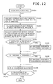
FIG. 12 is a flow chart for showing the process flow in the analysis device for the first embodiment of the present invention;
FIG. 13 is a graph for showing an example of the case of a correlation in time-based fluctuations among wavelengths;
FIG. 14 is a graph for showing an example of the case where there is no correlation in time-based fluctuations among wavelengths;
FIG. 15 is a drawing for showing an example of the display screen of the first embodiment of the present invention; and
FIG. 16 is a drawing for showing an example of the display screen of the first embodiment of the present invention.
DETAILED DESCRIPTION
The embodiments of the present invention are described next while referring to the accompanying drawings. In all drawings for describing the embodiments, the same reference numerals are generally attached to the same members, and their redundant descriptions are omitted.
[Etching Device]
In the present invention, the etching device 1 as shown in the block diagram in FIG. 1, includes an etching unit 10, analysis unit 20, input unit 30, output unit 31, and communication IF unit 32, and also a bus 33 to mutually connect these components.
The etching unit 10 includes a plasma machining unit 11, a spectroscope (OES) 12, a control unit 13, and an IF unit 14. The plasma machining unit 11 generates the plasma and machines the wafer, and while the etching is being performed, the spectroscope (OES) 12 obtains the light emission data from the plasma serving as the OES data. The OES data is stored by way of the IF unit 14, into the storage unit 22 contained in the analysis unit 20. The control unit 13 controls the processing by the plasma machining unit 11. The etching unit 10 is described in detail later while referring to FIG. 2.
The analysis unit 20 contains an arithmetic logic unit 21 to process the collected OES data, a storage unit 22 to store OES data, data showing the wavelength of the light emitted from each substance, and the processed results, and an IF unit 210. The arithmetic logic unit 21 obtains time-based data on the plural light emission intensities from the OES data, calculates the degree of similarity such as the correlation coefficient among the obtained time-based data, and performs processing to identify the wavelength required for monitoring, supervising, and controlling the etching process, from the extent of the degree of similarity. The processing by the arithmetic logic unit 21 is described in detail while referring to FIG. 13.
The input unit 30 is for example a mouse or keyboard that receives information input by user operation. The output unit 31 is a display or printer for outputting information to the user. The communication IF unit 32 is an interface connectable to other systems (also connectable to currently used production control systems etc.) by way of the bus 33 and an external network, and for sending and receiving information. The bus 33 couples each component (10, 20, 30, 31, and 32). Each IF unit (14, 29, etc.) are interfaces for sending and receiving information by way of the bus 33. The analysis unit 20 may also be connected as an analysis device outside of the etching device 1.
[Etching Unit]
The etching unit 10 is comprised of the plasma machining unit 11, a spectroscope (OES) 12, a control unit 13, and an IF unit 14. The plasma machining unit 11 includes a chamber 111, electrode 112 a and 112 b, a window 115, and a gas supply device 117. In response to instructions from the control unit 13, the plasma machining unit 11 stores the wafer 114 inside the chamber ill, supplies the etching gas from the gas supply device 117, and causes the gas 113 made into plasma to strike the wafer 114 by applying a voltage using the electrode 112 a and 112 b, to machine the wafer 114. The gas 113 contains substances in the etching gas supplied from the gas supply device 117 and substances generated in the wafer 114 from the machining process. A light 116 is emitted at a wavelength according to the substance contained in the gas. The emitted light passes through the window 115 and is measured by the spectroscope (OES) 12.
[OES Data]
FIG. 3 is a drawing for describing an example of the OES data measured by the spectroscope (OES) 12. The OES data contains two dimensional spatial and temporal elements, and expresses the light emission intensity value respectively measured at each wavelength and time. FIG. 4 is a graph for describing time-based fluctuations in light emission intensity at a specified wavelength. The light emission intensity value varies with the time as shown in FIG. 4. The locus of the time-based fluctuations varies with the wavelength.
[Analysis Unit]
The analysis unit 20 as shown in FIG. 1, includes an arithmetic logic unit 21, a storage unit 22, and an IF unit 210. The storage unit 22 contains a substance and matching wavelength table storage region 23, OES data storage region 24, identical substance correlating information storage region 25, peripheral wavelength correlating information storage region 26, threshold information storage region 27, and recommended wavelength information storage region 28.
Information specifying the wavelength of light 116 from the substance possible contained in the gas 113 is stored in the substance and matching wavelength table storage region 23. The substance is a single element or coupled from plural elements, and the wavelength of the light emitted from each substance is identified by measurements made beforehand. The substances as described here are not constantly contained in the gas 113. Moreover, if the wavelengths of light emitted from each substance are the same then the substances are identical even if the conditions for the etching device 1 are different.
FIG. 5 shows a substance and matching wavelength table 23 a serving as the first embodiment of the substance and matching wavelength table storage region 23. This table contains respective fields such as the substance field 23 b, and wavelength field 23 c, etc.
Information for identifying the substance possibly contained in the gas 113 is stored in the substance field 23 b.
Information for identifying the wavelength of light emitted from the substance specified in substance field 23 b is stored in the wavelength field 23 c. The wavelength specified by the wavelength field 23 c is made to correspond to one or a plurality of substances.
The light emission intensity value for wavelengths stored in the wavelength field 23 c among OES data might not necessarily always be determined by the light emission from a substance (stored on the same row) linked to the substance field 23 b. Therefore, monitoring, supervision, and control of the plasma machining unit 11 requires identifying a substance whose light emission intensity is determined by light emission from a substance linked to the substance field 23 b among the wavelengths stored in the wavelength field 23 c.
The OES data storage region 24 contains information specifying OES data measured by the spectroscope (OES) 12.
FIG. 6 shows the OES data table 24 a serving as the first embodiment of the OES data storage region 24. This table contains each field such as a wavelength field 24 b, time field 24 c, light emission intensity field 24 d, etc.
Information for identifying the wavelength of the measured OES data is stored in the wavelength field 24 b. Rows storing values identical to the values stored in wavelength field 23 c of the previously described substance and matching wavelength table 23 a are present in the wavelength field 24 b.
Information specifying the time of the measured OES data is stored in the time field 24 c.
Information for specifying the light emission intensity of the OES data for the wavelength specified via the wavelength field 24 b and the time specified via the time field 24 c is stored in the light emission intensity field 24 d.
Results from calculating the correlation coefficient serving as the degree of similarity for time-based data of light emission intensity for items applicable to the wavelength stored in the substance and matching wavelength table storage region 23 among OES data stored in the OES data storage region 24, are stored in the identical substance correlating information storage region 25.
FIG. 7 is a drawing showing an example of an identical substance correlating information table 25 a serving as the first embodiment of the identical substance correlating information storage region 25. This table contains each field such as a substance field 25 b, a wavelength field (column direction) 25 c, a wavelength field (row direction) 25 d, a light emission intensity correlation 1 field 25 e, etc.
Names for each substance emitting light on a wavelength specified by the values stored in wavelength field (column direction) 25 c and wavelength field (row direction) 25 d are stored in the substance field 25 b.
The substance specified by the value stored in the substance field 25 b, is stored in the wavelength field (column direction) 25 c as information specifying the wavelength linked via the substance and matching wavelength table 23 a.
Substances specified by the value stored in the substance field 25 b are stored in the wavelength field (row direction) 25 d, in the same way as the wavelength field (column direction) 25 c, as information specifying the wavelength linked via the substance and matching wavelength table 23 a.
The light emission intensity correlation 1 field 25 e stores information specifying the correlation coefficient serving as the degree of similarity for both time-based fluctuations in light emission intensity at a wavelength specified by a value stored in the wavelength field (column direction) 25 c; and time-based fluctuations in light emission intensity at a wavelength specified by a value stored in the wavelength field (row direction) 25 d. The above described time-based fluctuations in light emission intensity are values specified by way of the OES data table 24 a.
Results from calculating the correlation coefficient serving as the degree of similarity for time-based data for light emission intensity for an applicable wavelength stored in the substance and matching wavelength table storage region 23 among the OES data stored in the OES data storage region 24, are stored in the peripheral wavelength correlating information storage region 26.
FIG. 8 shows the peripheral wavelength correlating information table 26 a serving as the first embodiment of the peripheral wavelength correlating information storage region 26. This table contains each table such as a substance field 26 b, a wavelength field 26 c, a peripheral wavelength field 26 d, and a light emission intensity correlation 2 field 26 e.
The substance field 26 b stores each substance name corresponding to the value stored in the substance field 23 b of the substance and matching wavelength table 23 a.
The wavelength field 26 c stores values for wavelengths corresponding to values stored in the wavelength field 23 c of the substance and matching wavelength table 23 a.
The peripheral wavelength field 26 d stores information showing the peripheral range of the wavelengths, with wavelengths specified by values stored in the wavelength field 26 c utilized as a reference standard. In the example in FIG. 8, a value where 50 was subtracted from the value stored in wavelength field 26 c, up to a value where 50 was added to the value stored in the wavelength field 26 c are stored in the peripheral wavelength field 26 d, however a value other than 50 may be utilized, and the subtracted value and the added value may be mutually different values.
The light emission intensity correlation 2 field 26 e stores information specifying the correlation coefficient serving as the degree of similarity, for time-based fluctuations for light emission intensity in the wavelength specified by the value stored in the wavelength field 26 c; and the averaged time-based fluctuations for light emission intensity in the wavelength range specified by the value stored in the peripheral wavelength field 26 d. The above described time-based fluctuations in light emission intensity are values specified via the OES data table 24 a. The above described averaged time-based fluctuations for light emission intensity are values specified via the light emission intensity average information table 29 a described later on.
Conditions for selecting a wavelength suitable for use in monitoring, supervision, and control of the etching unit 10 are stored in the threshold information storage region 27.
FIG. 9 shows the threshold information table 27 a serving as the first embodiment of the threshold information storage region 27. This table contains each field such as the threshold value 1 field 27 b, threshold value 2 field 27 c, and threshold value 3 field 27 d, etc.
The threshold value 1 field 27 b stores information for specifying the cell storing a large correlation coefficient for the light emission intensity correlation 1 field 25 e of the identical substance correlating information table 25 a.
The threshold value 2 field 27 c stores information for specifying the wavelength to serve as the recommended wavelength, by using information stored in the identical substance correlating information table 25 a.
The threshold value 3 field 27 d stores information for specifying the wavelength to serve as the recommended wavelength, by using information stored in the peripheral wavelength correlating information table 26 a.
The recommended wavelength information storage region 28 stores information used for specifying the wavelength to be utilized for monitoring, supervision, and control of the etching unit 10 from among the wavelengths stored in the substance and matching wavelength table storage region 23.
FIG. 10 shows the recommended wavelength information table 28 a serving as the first embodiment of the recommended wavelength information storage region 28. This table includes each field such as the substance field 28 b, the wavelength field 28 c, and the recommended wavelength field 28 d, etc.
The substance field 28 b stores the name of the substance corresponding to the values stored in the substance field 23 b in the substance and matching wavelength table 23 a.
The wavelength field 28 c stores the value of the wavelength corresponding to the value stored in the wavelength field 23 c of the substance and matching wavelength table 23 a.
The recommended wavelength field 28 d stores information for specifying the wavelength ideal for use in monitoring, supervision, and control of the etching unit 10 from the wavelengths specified by way of the value stored in the wavelength field 28 c.
The light emission intensity average information storage region 29 stores information for specifying the value that the OES data stored in the OES data storage region 24 is averaged in the specified wavelength zone.
FIG. 11 shows the light emission intensity average information table 29 a serving as the first embodiment of the light emission intensity average information storage region 29. This table contains each field such as peripheral wavelength field 29 b, time field 29 c, and light emission intensity average field 29 d, etc.
The peripheral wavelength field 29 b stores information specifying the peripheral range of the wavelength whose calculated light emission intensity average was specified by way of a value stored in the light emission intensity average field 29 d.
The time field 29 c stores information for specifying the measured time of the light emission intensity average specified by way of the value stored in the light emission intensity average field 29 d.
Information specifying averaged results in a range specified by way of a value stored in the peripheral wavelength field 29 b, from values stored in the light emission intensity field 24 d of OES data table 24 a is stored in the light emission intensity average field 29 d.
[Analysis Process by Analysis Unit 20]
FIG. 12 shows analysis processing (expressed in processing steps such as S101) performed mainly by the arithmetic logic unit 21 in the analysis unit 20. The analysis process is described while referring to FIG. 12.
The arithmetic logic unit 21 implements the analysis processing shown in FIG. 12 when the etching processing by the etching unit 10 ends or the user inputs a command to execute the analysis process. The respective values are stored in the substance and matching wavelength table 23 a, the OES data table 24 a, and the threshold information table 27 a, at the stage where executing the analysis process. The values measured in past testing is stored in the substance and matching wavelength table 23 a, the values measured by the spectroscope (OES) 12 is stored in the OES data table 24 a, and the values set by the designer is stored in the threshold information table 27 a.
(S101)
In S101, the arithmetic logic unit 21 stores the required data for calculation in each data table.
First of all, the arithmetic logic unit 21 stores the value stored in the substance field 23 b in the substance and matching wavelength table 23 a, into the substance field 26 b of the peripheral wavelength correlating information table 26 a, and stores the value stored in the wavelength field 23 c of the substance and matching wavelength table 23 a, into the wavelength field 26 c.
The arithmetic logic unit 21 also stores the value stored in the substance field 23 b in the substance and matching wavelength table 23 a, into the substance field 28 b of the recommended wavelength information storage table 28 a, and stores the value stored in the wavelength field 23 c of the substance and matching wavelength table 23 a, into the wavelength field 28 c.
The arithmetic logic unit 21 further stores the value stored in the time field 24 c of the OES data table 24 a into the time field 29 c of the light emission intensity average information table 29 a.
When step S101 ends, the arithmetic logic unit 21 stores a in the value i showing a row number in the substance and matching wavelength table 23 a.
(S102)
In S102, the arithmetic logic unit 21 calculates the correlation of the time-based data for light emission intensity between identical substances, using information in the OES data table 24 as input, and stores the calculated correlation in the identical substance correlating information table 25 a.
First of all, the arithmetic logic unit 21 deletes all data in the identical substance correlating information table 25 a.
The arithmetic logic unit 21 loads the value (substance i) stored in the i-th row of the substance field 23 b in the substance and matching wavelength table 23 a, and stores the value in the substance field 25 b of the identical substance correlating information table 25 a.
The arithmetic logic unit 21 scans the substance field 23 b in the substance and matching wavelength table 23 a from the first row to the final row, and for the row storing a value identical to substance i, stores the value stored on the applicable row of wavelength field 23 c into the final column of wavelength field (column direction) 25 c, and final row of wavelength field (row direction) 25 d. If there is already a value stored in the final column then one column is added to the final column, and the value stored in the applicable column. Also, if there is already a value stored in the final row, one row is added to the final row in the same way, and the value stored in the applicable row. This process stores a value identifying a wavelength corresponding to substance i, in the wavelength field (column direction) 25 c and wavelength field (row direction) 25 d of the identical substance correlating information table 25 a.
The arithmetic logic unit 21 further stores the value in the light emission intensity correlation 1 field 25 e. By setting the column number of wavelength field (column direction) 25 c as j, and the row number of wavelength field (row direction) as k, the value (r1) stored in k row j column of light emission intensity correlation 1 field 25 e can be calculated by way of the following formula (1).
The significance of each symbol in formula (1) is given as follows.
Here in wavelength field 24 b of OES data table 24 a, the symbol p denotes the column number storing a value identical to the value stored in the j column of wavelength field (column direction) 25 c.
In wavelength field 24 b of OES data table 24 a, the symbol q denotes the column number storing a value identical to the value stored in the k row of the wavelength field (row direction) 25 d.
The symbol xlp denotes the value stored in l row p column, among the values stored in the light emission intensity field 24 d of the OES data table 24 a.
The symbol xmp denotes the value stored in m row p column among the values stored in the light emission intensity field 24 d of the OES data table 24 a.
The symbol xlq denotes the value stored in l row q column among the values stored in the light emission intensity field 24 d of the OES data table 24 a.
The symbol xmq denotes the value stored in m row q column among the values stored in the light emission intensity field 24 d of the OES data table 24 a.
The symbol n expresses the number of rows of the light emission intensity field 24 d in the OES data table 24 a.
The symbol r1 is the value (correlation coefficient) calculated in formula (1). The symbol r1 expresses the extent of the degree of similarity of the time-based fluctuation for the value stored in the p column of light emission intensity field 24 d, and the value stored in the q column of light emission intensity field 24 d.
FIG. 13 is graphs of the time-based fluctuations in light emission intensity, and shows the value for correlation coefficient r1 among the time-based fluctuations expressed in these two graphs. The time-based fluctuations in the two graphs are similar, and a large correlation coefficient r1 can also be observed.
The formula (1) utilizes a correlation coefficient but other indices for evaluating the degree of similarity may also be utilized.
The arithmetic logic unit 21 calculates the correlation coefficient using formula (1) for all combinations of rows and columns in light emission intensity correlation 1 field 25 e, and stores the calculated value.
(S103)
In S103, the arithmetic logic unit 21 inputs information from OES data table 24 a, calculates the average value of light emission intensity on wavelengths peripheral to the wavelength of the i-th row, and stores that average value in the light emission intensity average information table 29 a.
The arithmetic logic unit 21 first of all loads the value stored in the i-th row of wavelength field 23 c into the substance and matching wavelength table 23 a, and sets the peripheral range of the wavelength using the loaded value as a reference. In the present embodiment, a value where 50 is subtracted from the loaded value is set as the minimum value, and a value where 50 is added to the loaded value is set as the maximum value.
The arithmetic logic unit 21 stores the set range in a “Minimum value range to maximum value range” format in the i-th row of peripheral wavelength field 26 d in the peripheral wavelength correlating information table 26 a, and in the peripheral wavelength field 29 b of the light emission intensity average information table 29 a.
The arithmetic logic unit 21 next calculates the average value for light emission intensity on the peripheral wavelength using the following formula (2), from the first row to the final row of the light emission intensity field 24 d in the OES data table 24, and stores the calculated value (AVEo) in the light emission intensity average field 29 d of the light emission intensity average information table 29 a.
The meaning of each symbol in formula (2) is given as follows.
Here, the symbol o denotes the row number for the light emission intensity 24 d in the OES data table 24.
The symbol Xos denotes the value stored in o row s column among the values stored in the light emission intensity field 24 d of the OES data table 24 a.
The symbol λs denotes the value stored in the s column, among the values stored in the wavelength field 24 b of the OES data table 24 a.
The symbol λmin denotes the minimum value stored in the above described range.
The symbol λmax denotes the maximum value stored in the above described range.
The symbol λi denotes the value stored in the i-th row of the wavelength field 23 c in the substance and matching wavelength table 23 a.
The symbol u denotes the number of columns in the wavelength field 24 c of the OES data table 24 a.
The symbol AVEo denotes the value stored in the o row of the light emission intensity average field 29 d in the light emission intensity average information table 29 a.
The formula (2) signifies the calculation of the average of the light emission intensity for a wavelength, contained in the range of values stored on the i-th row of the peripheral wavelength field 26 d in the peripheral wavelength correlating information table 26 a, and also not matching the value stored on the i-th row of the wavelength field 23 c in the substance and matching wavelength table 23 a. The light emission intensity for a wavelength matching the value stored on the i-th row is here excluded from the calculation of the average value but may also be included in the calculation.
(S104)
In step S104, the arithmetic logic unit 21 calculates the correlation of the time-based data for light emission intensity between information stored in the light emission intensity field 24 d of the OES data table 24 a, and the information stored in the light emission intensity average field 29 d of the light emission intensity average information table 29 a, and stores the calculated value in the light emission intensity correlation 2 field 26 e of the peripheral wavelength correlating information table 26 a.
The arithmetic logic unit 21 stores the value (r2) calculated by the following formula (3), into the i-th row of the light emission intensity correlation 2 field 26 e.
The meaning of each symbol in formula (3) is given as follows.
Here, the symbol p denotes the column number storing a value identical to the value in the i-th row of the wavelength field 23 c is stored in the wavelength field 24 b of the OES data table 24 a.
The symbol Xlp denotes the value stored in l row p column among the values stored in the light emission intensity field 24 d of the OES data table 24 a.
The symbol yl denotes the value stored in l row among the values stored in the light emission intensity average field 29 d of the light emission intensity average information table 29 a.
The symbol n expresses the number of rows of the light emission intensity field 24 d in the OES data table 24 a.
The symbol r2 is a value (correlation coefficient) calculated in formula (3). The symbol r2 expresses the extent of the degree of similarity of the time-based fluctuation between the value stored in the p column of the light emission intensity field 24 d in the OES data table 24 a, and the value stored in the q column in the light emission intensity field 24 d.
The formula (3) utilized a coefficient correlation but other indices for evaluating the degree of similarity may also be utilized.
(S105)
In step S105, the arithmetic logic unit 21 utilizes the information stored in the identical substance correlating information table 25 a to judge whether or not the wavelength specified by way of the value stored on the i-th row of wavelength field 23 c in the substance and matching wavelength table 23 a is the wavelength capable of being utilized for monitoring, supervision and control of the etching unit 10.
The arithmetic logic unit 21 utilizes the value stored in the light emission intensity correlation 1 field 25 e of the identical substance correlating information table 25 a as an input, to calculate by way of the following formula (4) the percentage (R1) by which the value stored in the light emission intensity correlation 1 field 25 e is larger than the value stored in the threshold value 1 field 27 b of the threshold information table 27 a.
The meaning of each symbol in formula (4) is given as follows.
The symbol v denotes the row number storing a value identical to the value stored in the i-th row of the wavelength field period 23 c, into the wavelength field (row direction) 25 d of the identical substance correlating information table 25 a.
The symbol w is the value for specifying the column number of the light emission intensity correlation 1 field 25 e of the identical substance correlating information table 25 a.
The symbol a denotes the number of columns in the light emission intensity correlation 1 field 25 e of the identical substance correlating information table 25 a.
The symbol ZVW denotes the value stored in the v row w column among the values stored in the light emission intensity correlation 1 field 25 e of the identical substance correlating information table 25 a.
The symbol Th1 denotes the value stored in the threshold value 1 field 27 b of the threshold information table 27 a.
The symbol λv denotes the value stored in the v row, among the values stored in the wavelength field (row direction) 25 d in the identical substance correlating information table 25 a.
The symbol λw denotes the value stored in the w column, among the values stored in the wavelength field (column direction) in the identical substance correlating information table 25 a.
The symbol R1 is a calculated value and indicates the percentage by which the correlation coefficient for light emission intensity of the wavelength specified by the value stored in the i-th row of the wavelength field 23 c of the substance and matching wavelength table 23 a is larger than the value specified in the threshold 1 field 27 b. A large R1 value indicates that the light emission intensity on the wavelength linked to the identical substance has similar time-based fluctuations. The reason for the similar time-based fluctuations is likely caused by increases or decreases in the quantity of that corresponding substance (if the quantity of the substance is increased, then the light emission intensity on the wavelength linked to that substance will increase as the quantity of that substance increases). By making use of this type of light emission intensity for monitoring, supervision, and control of the etching unit 10, the quantity of the substance contained in the gas 113 can be known, and monitoring, supervision, and control of the etching unit 10 can be effectively implemented.
Based on the above approach, the arithmetic logic unit 21 next compares the R1 with the value stored in the threshold value 2 field 27 c, and if R1 is a value equal to or larger than the value stored in the threshold value 2 field 27 c, then the arithmetic logic unit 21 judges that the wavelength identified by the value stored in the i-th row of the wavelength field 23 c in the substance and matching wavelength table 23 a is the wavelength capable of being utilized for monitoring, supervision, and control of the etching unit 10, and the arithmetic logic unit 21 proceeds to the process in S106.
If R1 is a value smaller than the value stored in the threshold value 2 field 27 c, then the arithmetic logic unit 21 proceeds to the process in S107.
(S106)
In S106, the arithmetic logic unit 21 stores the value “recommend 1” showing the judgment that the wavelength is capable of being utilized for monitoring, supervision, and control of the etching unit 10, into the i-th row of the recommended wavelength field 28 d in recommended wavelength information table 28 a.
(S107)
In S107, the arithmetic logic unit 21 utilizes the information stored in the identical substance correlating information table 25 a to decide whether or not the wavelength specified by the value stored in the i-th row of wavelength field 23 c in the substance and matching wavelength table 23 a is the wavelength capable of being utilized for monitoring, supervision, and control of the etching unit 10.
The arithmetic logic unit 21 compares the value stored in the light emission intensity correlation 2 field 26 e of peripheral wavelength correlating information table 26 a, with the value stored in threshold value 3 field 27 d of the threshold information table 27 a. If the value stored in the light emission intensity correlation 2 field 26 e is smaller than the value stored in the threshold value 3 field 27 d, the waveform specified by the value stored in the i-th row of wavelength field 23 c of the substance and matching wavelength table 23 a is judged as the wavelength capable of being utilized for monitoring, supervision, and control of the etching unit 10, and the arithmetic logic unit 21 proceeds to the process in S108.
However, if the value stored in the light emission intensity correlation 2 field 26 e of the peripheral wavelength correlating information table 26 a is small, the small value signifies that the degree of similarity between the time-based fluctuations in light emission intensity on the wavelength specified by the value stored in the i-th row of the waveform field 23 c of the substance and matching wavelength table 23 a, and average of time-based fluctuations for light emission intensity on the peripheral wavelength is small as shown in FIG. 14. In this case, the increase or decrease in the light emission intensity on the applicable wavelength is likely caused by factors such as the temperature and amount of that corresponding substance. Using the light emission intensity on this type of wavelength to monitor, supervise, and control the etching unit 10 permits knowing factors such as the temperature and amount of the substance contained in the gas 113, and the monitoring, supervision, and control of the etching unit 10 can be effectively implemented.
If the value stored in the light emission intensity correlation 2 field 26 e is larger than the value stored in the threshold value 3 field 27 d, the arithmetic logic unit 21 proceeds to the process in S109.
(S108)
In S108, the arithmetic logic unit 21 stores the value for “recommend 2” showing the judgment that the wavelength is capable of being utilized for monitoring, supervision, and control of the etching unit 10, into the i-th row of the recommended wavelength field 28 d in the recommended wavelength information table 28 a. If a value for “recommend 1” is already stored then “recommend 1” and “recommend 2” are both jointly recorded.
(S109)
In S109, if the processing in S106 or S108 was executed, the arithmetic logic unit 21 performs processing to provide a wavelength capable of being utilized for monitoring, supervision, and control of the etching unit 10 to the user.
If there is a value for “recommend 1” stored in the i-th row in the recommended wavelength field 28 d of the recommended wavelength information table 28 a, the arithmetic logic unit 21 displays information as shown for example in FIG. 15 on the output unit 31.
The arithmetic logic unit 21 displays the wavelength (value stored in the i-th row of the wavelength field 23 c of the substance and matching wavelength table 23 a) recommended for utilization in device control and quality analysis, that is judged as the wavelength exhibiting light emitted from a substance contained in the plasma within the chamber; and the name of the substance corresponding to that wavelength (value stored in the i-th row of the substance field 23 b of the substance and matching wavelength table 23 a).
The arithmetic logic unit 21 also displays the correlation coefficient (value stored in the light emission intensity correlation 1 field 25 e of the identical substance correlating information table 25 a) between the time-based fluctuations for light emission intensity in the recommended wavelength, and the time-based fluctuations for light emission intensity in the wavelength from the same substance as the recommended wavelength.
The arithmetic logic unit 21 further displays a graph of the time-based fluctuations for light emission intensity in the recommended wavelength, and the time-based fluctuations (value stored in the light emission intensity field 24 d of the OES data table 24 a) for light emission intensity in the wavelength from the same substance as the recommended wavelength.
If there is a value for “recommend 2” stored in the i-th row of the recommended wavelength field 28 d of the recommended wavelength information table 28 a, the arithmetic logic unit 21 displays information as shown for example in FIG. 16 on the output unit 31.
The arithmetic logic unit 21 displays the recommended wavelength (value stored in the i-th row of the wavelength field 23 c of the substance and matching wavelength table 23 a) and the name of the substance corresponding to that wavelength (value stored in the i-th row of the substance field 23 b of the substance and matching wavelength table 23 a).
The arithmetic logic unit 21 also displays the correlation coefficient (value stored in the light emission intensity correlation 2 field 26 e of the peripheral wavelength correlating information table 26 a) between the time-based fluctuations for light emission intensity in the recommended wavelength, and the time-based fluctuations for the light emission intensity average on the recommended peripheral wavelength.
The arithmetic logic unit 21 further displays a graph of time-based fluctuations (value stored in the light emission intensity field 24 d of OES data table 24 a) for light emission intensity in the recommended wavelength; and the time-based fluctuations (value stored in light emission intensity average field 29 d of the light emission intensity average information table 29 a) for the light emission intensity in the wavelength from the same substance as the recommended wavelength.
(S110)
In S110, the arithmetic logic unit 21 ends the process when the process has reached the final row of wavelength field 23 c of the substance and matching wavelength table 23 a, and adds a 1 to if the process has not reached the final row, and executes the calculation for the next row of the wavelength field 23 c in the substance and matching wavelength table 23 a.
As described above, in the etching device 1 (analysis unit 20) of the present embodiment, the data measured by the spectroscope (OES), and information on the wavelength of light emitted by each substance can be provided as input information to provide a wavelength that allows knowing properties (such as the temperature and amount of substance contained in the gas 113) of the gas 113. By using the light emission intensity of the provided wavelength as an input, the control unit 13 of the etching unit 1 can perform the etching process with higher efficiency by appropriately controlling factors such as the quantity of gas, temperature, and voltage supplied to the chamber 111.
Moreover, a wavelength utilizable for monitoring, supervision, and control is automatically be selected from many candidates among wavelengths in the OES data so that the large quantity of man-hours required for analyzing the etching data can be eliminated and monitoring, supervising, and control of the etching can be efficiently performed.
The embodiment of the present invention was specifically described above, however the present invention is not limited to the above embodiment and all manner of variations and adaptations not departing from the scope of the present invention are permissible.