US9466552B2 - Vertical semiconductor device having a non-conductive substrate and a gallium nitride layer - Google Patents
Vertical semiconductor device having a non-conductive substrate and a gallium nitride layer Download PDFInfo
- Publication number
- US9466552B2 US9466552B2 US13/436,665 US201213436665A US9466552B2 US 9466552 B2 US9466552 B2 US 9466552B2 US 201213436665 A US201213436665 A US 201213436665A US 9466552 B2 US9466552 B2 US 9466552B2
- Authority
- US
- United States
- Prior art keywords
- electrode
- conductive
- semiconductor layer
- substrate
- type impurities
- Prior art date
- Legal status (The legal status is an assumption and is not a legal conclusion. Google has not performed a legal analysis and makes no representation as to the accuracy of the status listed.)
- Active, expires
Links
- 239000004065 semiconductor Substances 0.000 title claims abstract description 62
- 239000000758 substrate Substances 0.000 title claims abstract description 43
- JMASRVWKEDWRBT-UHFFFAOYSA-N Gallium nitride Chemical compound [Ga]#N JMASRVWKEDWRBT-UHFFFAOYSA-N 0.000 title description 12
- 229910002601 GaN Inorganic materials 0.000 title description 10
- 239000012535 impurity Substances 0.000 claims description 21
- 210000000746 body region Anatomy 0.000 claims description 11
- 229910052594 sapphire Inorganic materials 0.000 claims description 9
- 239000010980 sapphire Substances 0.000 claims description 9
- HBMJWWWQQXIZIP-UHFFFAOYSA-N silicon carbide Chemical compound [Si+]#[C-] HBMJWWWQQXIZIP-UHFFFAOYSA-N 0.000 claims description 7
- 238000002347 injection Methods 0.000 claims description 4
- 239000007924 injection Substances 0.000 claims description 4
- 229910010271 silicon carbide Inorganic materials 0.000 claims description 3
- 238000004519 manufacturing process Methods 0.000 abstract description 12
- 238000010586 diagram Methods 0.000 description 3
- 238000010329 laser etching Methods 0.000 description 3
- 230000004888 barrier function Effects 0.000 description 2
- 230000007423 decrease Effects 0.000 description 2
- 238000000034 method Methods 0.000 description 2
- 238000012986 modification Methods 0.000 description 2
- 230000004048 modification Effects 0.000 description 2
- RNQKDQAVIXDKAG-UHFFFAOYSA-N aluminum gallium Chemical compound [Al].[Ga] RNQKDQAVIXDKAG-UHFFFAOYSA-N 0.000 description 1
- 239000000969 carrier Substances 0.000 description 1
- 239000013078 crystal Substances 0.000 description 1
- 230000003247 decreasing effect Effects 0.000 description 1
- 230000000694 effects Effects 0.000 description 1
- 239000011810 insulating material Substances 0.000 description 1
Images


Classifications
-
- H—ELECTRICITY
- H01—ELECTRIC ELEMENTS
- H01L—SEMICONDUCTOR DEVICES NOT COVERED BY CLASS H10
- H01L23/00—Details of semiconductor or other solid state devices
- H01L23/52—Arrangements for conducting electric current within the device in operation from one component to another, i.e. interconnections, e.g. wires, lead frames
- H01L23/535—Arrangements for conducting electric current within the device in operation from one component to another, i.e. interconnections, e.g. wires, lead frames including internal interconnections, e.g. cross-under constructions
-
- H—ELECTRICITY
- H01—ELECTRIC ELEMENTS
- H01L—SEMICONDUCTOR DEVICES NOT COVERED BY CLASS H10
- H01L23/00—Details of semiconductor or other solid state devices
- H01L23/48—Arrangements for conducting electric current to or from the solid state body in operation, e.g. leads, terminal arrangements ; Selection of materials therefor
- H01L23/481—Internal lead connections, e.g. via connections, feedthrough structures
-
- H—ELECTRICITY
- H01—ELECTRIC ELEMENTS
- H01L—SEMICONDUCTOR DEVICES NOT COVERED BY CLASS H10
- H01L29/00—Semiconductor devices adapted for rectifying, amplifying, oscillating or switching, or capacitors or resistors with at least one potential-jump barrier or surface barrier, e.g. PN junction depletion layer or carrier concentration layer; Details of semiconductor bodies or of electrodes thereof ; Multistep manufacturing processes therefor
- H01L29/66—Types of semiconductor device ; Multistep manufacturing processes therefor
- H01L29/66007—Multistep manufacturing processes
- H01L29/66075—Multistep manufacturing processes of devices having semiconductor bodies comprising group 14 or group 13/15 materials
- H01L29/66083—Multistep manufacturing processes of devices having semiconductor bodies comprising group 14 or group 13/15 materials the devices being controllable only by variation of the electric current supplied or the electric potential applied, to one or more of the electrodes carrying the current to be rectified, amplified, oscillated or switched, e.g. two-terminal devices
- H01L29/66196—Multistep manufacturing processes of devices having semiconductor bodies comprising group 14 or group 13/15 materials the devices being controllable only by variation of the electric current supplied or the electric potential applied, to one or more of the electrodes carrying the current to be rectified, amplified, oscillated or switched, e.g. two-terminal devices with an active layer made of a group 13/15 material
- H01L29/66204—Diodes
- H01L29/66212—Schottky diodes
-
- H—ELECTRICITY
- H01—ELECTRIC ELEMENTS
- H01L—SEMICONDUCTOR DEVICES NOT COVERED BY CLASS H10
- H01L29/00—Semiconductor devices adapted for rectifying, amplifying, oscillating or switching, or capacitors or resistors with at least one potential-jump barrier or surface barrier, e.g. PN junction depletion layer or carrier concentration layer; Details of semiconductor bodies or of electrodes thereof ; Multistep manufacturing processes therefor
- H01L29/66—Types of semiconductor device ; Multistep manufacturing processes therefor
- H01L29/66007—Multistep manufacturing processes
- H01L29/66075—Multistep manufacturing processes of devices having semiconductor bodies comprising group 14 or group 13/15 materials
- H01L29/66227—Multistep manufacturing processes of devices having semiconductor bodies comprising group 14 or group 13/15 materials the devices being controllable only by the electric current supplied or the electric potential applied, to an electrode which does not carry the current to be rectified, amplified or switched, e.g. three-terminal devices
- H01L29/66234—Bipolar junction transistors [BJT]
- H01L29/6631—Bipolar junction transistors [BJT] with an active layer made of a group 13/15 material
-
- H—ELECTRICITY
- H01—ELECTRIC ELEMENTS
- H01L—SEMICONDUCTOR DEVICES NOT COVERED BY CLASS H10
- H01L29/00—Semiconductor devices adapted for rectifying, amplifying, oscillating or switching, or capacitors or resistors with at least one potential-jump barrier or surface barrier, e.g. PN junction depletion layer or carrier concentration layer; Details of semiconductor bodies or of electrodes thereof ; Multistep manufacturing processes therefor
- H01L29/66—Types of semiconductor device ; Multistep manufacturing processes therefor
- H01L29/66007—Multistep manufacturing processes
- H01L29/66075—Multistep manufacturing processes of devices having semiconductor bodies comprising group 14 or group 13/15 materials
- H01L29/66227—Multistep manufacturing processes of devices having semiconductor bodies comprising group 14 or group 13/15 materials the devices being controllable only by the electric current supplied or the electric potential applied, to an electrode which does not carry the current to be rectified, amplified or switched, e.g. three-terminal devices
- H01L29/66234—Bipolar junction transistors [BJT]
- H01L29/66325—Bipolar junction transistors [BJT] controlled by field-effect, e.g. insulated gate bipolar transistors [IGBT]
- H01L29/66333—Vertical insulated gate bipolar transistors
-
- H—ELECTRICITY
- H01—ELECTRIC ELEMENTS
- H01L—SEMICONDUCTOR DEVICES NOT COVERED BY CLASS H10
- H01L29/00—Semiconductor devices adapted for rectifying, amplifying, oscillating or switching, or capacitors or resistors with at least one potential-jump barrier or surface barrier, e.g. PN junction depletion layer or carrier concentration layer; Details of semiconductor bodies or of electrodes thereof ; Multistep manufacturing processes therefor
- H01L29/66—Types of semiconductor device ; Multistep manufacturing processes therefor
- H01L29/68—Types of semiconductor device ; Multistep manufacturing processes therefor controllable by only the electric current supplied, or only the electric potential applied, to an electrode which does not carry the current to be rectified, amplified or switched
- H01L29/70—Bipolar devices
- H01L29/72—Transistor-type devices, i.e. able to continuously respond to applied control signals
- H01L29/73—Bipolar junction transistors
- H01L29/732—Vertical transistors
-
- H—ELECTRICITY
- H01—ELECTRIC ELEMENTS
- H01L—SEMICONDUCTOR DEVICES NOT COVERED BY CLASS H10
- H01L29/00—Semiconductor devices adapted for rectifying, amplifying, oscillating or switching, or capacitors or resistors with at least one potential-jump barrier or surface barrier, e.g. PN junction depletion layer or carrier concentration layer; Details of semiconductor bodies or of electrodes thereof ; Multistep manufacturing processes therefor
- H01L29/66—Types of semiconductor device ; Multistep manufacturing processes therefor
- H01L29/68—Types of semiconductor device ; Multistep manufacturing processes therefor controllable by only the electric current supplied, or only the electric potential applied, to an electrode which does not carry the current to be rectified, amplified or switched
- H01L29/70—Bipolar devices
- H01L29/72—Transistor-type devices, i.e. able to continuously respond to applied control signals
- H01L29/739—Transistor-type devices, i.e. able to continuously respond to applied control signals controlled by field-effect, e.g. bipolar static induction transistors [BSIT]
- H01L29/7393—Insulated gate bipolar mode transistors, i.e. IGBT; IGT; COMFET
- H01L29/7395—Vertical transistors, e.g. vertical IGBT
-
- H—ELECTRICITY
- H01—ELECTRIC ELEMENTS
- H01L—SEMICONDUCTOR DEVICES NOT COVERED BY CLASS H10
- H01L29/00—Semiconductor devices adapted for rectifying, amplifying, oscillating or switching, or capacitors or resistors with at least one potential-jump barrier or surface barrier, e.g. PN junction depletion layer or carrier concentration layer; Details of semiconductor bodies or of electrodes thereof ; Multistep manufacturing processes therefor
- H01L29/66—Types of semiconductor device ; Multistep manufacturing processes therefor
- H01L29/86—Types of semiconductor device ; Multistep manufacturing processes therefor controllable only by variation of the electric current supplied, or only the electric potential applied, to one or more of the electrodes carrying the current to be rectified, amplified, oscillated or switched
- H01L29/861—Diodes
- H01L29/872—Schottky diodes
-
- H—ELECTRICITY
- H01—ELECTRIC ELEMENTS
- H01L—SEMICONDUCTOR DEVICES NOT COVERED BY CLASS H10
- H01L29/00—Semiconductor devices adapted for rectifying, amplifying, oscillating or switching, or capacitors or resistors with at least one potential-jump barrier or surface barrier, e.g. PN junction depletion layer or carrier concentration layer; Details of semiconductor bodies or of electrodes thereof ; Multistep manufacturing processes therefor
- H01L29/02—Semiconductor bodies ; Multistep manufacturing processes therefor
- H01L29/12—Semiconductor bodies ; Multistep manufacturing processes therefor characterised by the materials of which they are formed
- H01L29/20—Semiconductor bodies ; Multistep manufacturing processes therefor characterised by the materials of which they are formed including, apart from doping materials or other impurities, only AIIIBV compounds
- H01L29/2003—Nitride compounds
-
- H—ELECTRICITY
- H01—ELECTRIC ELEMENTS
- H01L—SEMICONDUCTOR DEVICES NOT COVERED BY CLASS H10
- H01L2924/00—Indexing scheme for arrangements or methods for connecting or disconnecting semiconductor or solid-state bodies as covered by H01L24/00
-
- H—ELECTRICITY
- H01—ELECTRIC ELEMENTS
- H01L—SEMICONDUCTOR DEVICES NOT COVERED BY CLASS H10
- H01L2924/00—Indexing scheme for arrangements or methods for connecting or disconnecting semiconductor or solid-state bodies as covered by H01L24/00
- H01L2924/0001—Technical content checked by a classifier
- H01L2924/0002—Not covered by any one of groups H01L24/00, H01L24/00 and H01L2224/00
Definitions
- the present invention relates to a vertical semiconductor device and a manufacturing method of a vertical semiconductor device; particularly, it relates to such vertical semiconductor device and manufacturing method wherein the current crowding phenomenon of a device is mitigated.
- GaN gallium nitride
- SiC silicon carbide
- sapphire substrate sapphire substrate
- SiN gallium nitride
- Sapphire is an insulating material, so if a power device is to be manufactured on the sapphire substrate, it has to be formed laterally; that is, the electrodes of the power device are formed on the same side of the substrate. This increases the area of the power device and the manufacturing cost, and also induces the current crowding problem.
- the present invention proposes a vertical semiconductor device and a manufacturing method thereof which decrease the device area such that the manufacturing cost is decreased, and mitigate the current crowding problem.
- a first objective of the present invention is to provide a vertical semiconductor device.
- a second objective of the present invention is to provide a manufacturing method of a vertical semiconductor device.
- the present invention provides a vertical semiconductor device, including: a substrate having a first surface and a second surface facing opposite directions, the substrate including a conductive array formed by a plurality of conductive plugs through the substrate; a semiconductor layer formed on the first surface, the semiconductor layer having a third surface and a fourth surface facing opposite directions, wherein the fourth surface faces the first surface; a first electrode formed on the third surface; and a second electrode formed on the second surface, for electrically connecting to the conductive array.
- the present invention provides a manufacturing method of a vertical semiconductor device, including: providing a substrate, which has a first surface and a second surface facing opposite directions; forming a semiconductor layer on the first surface, which has a third surface and a fourth surface facing opposite directions, wherein the fourth surface faces the first surface; forming a first electrode on the third surface; forming a plurality of holes through the substrate, the holes forming a hole array; forming a plurality of conductive plugs in the holes to form a conductive array; and forming a second electrode on the second surface for electrically connecting to the conductive array.
- the substrate preferably includes a silicon carbide (SiC) substrate or a sapphire substrate.
- SiC silicon carbide
- the semiconductor layer preferably includes a gallium nitride (GaN) layer, and the first electrode, the GaN layer, the conductive array, and the second electrode form a vertical Schottky barrier diode (SBD).
- GaN gallium nitride
- SBD vertical Schottky barrier diode
- the semiconductor layer preferably includes: a GaN layer doped with first conductive type impurities; a base region doped with second conductive type impurities, the base region being formed in the GaN layer and electrically connected to the first electrode; and an emitter region doped with first conductive type impurities, the emitter region being formed in the base region and electrically connected to a third electrode which is formed on the third surface; wherein the first electrode, the semiconductor layer, the third electrode, the conductive array, and the second electrode form a vertical bipolar junction transistor (BJT).
- BJT vertical bipolar junction transistor
- the semiconductor layer includes: a GaN layer doped with first conductive type impurities; a body region doped with second conductive type impurities, the body region being formed in the GaN layer and electrically connected to the first electrode; an emitter region doped with first conductive type impurities, the emitter region being formed in the body region and electrically connected to the first electrode; and an injection region doped with second conductive type impurities, the injection region being formed between the GaN layer and the substrate, and being electrically connected to the second electrode by the conductive array.
- the vertical semiconductor device further includes: a dielectric layer formed on the third surface; and a gate formed on the dielectric layer.
- FIGS. 1A-1D show a first embodiment of the present invention.
- FIGS. 2A-2D show a second embodiment of the present invention.
- FIGS. 3A-3D show a third embodiment of the present invention.
- FIGS. 1A-1D show a first embodiment of the present invention.
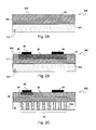
- FIGS. 1A-1D are schematic cross-section diagrams showing a manufacturing flow of a Schottky barrier diode (SBD) 100 according to this embodiment.
- a substrate 11 is provided, which has an upper surface 111 and a lower surface 112 .
- the substrate 11 for example is but not limited to a silicon carbide (SiC) substrate or a sapphire substrate.
- a semiconductor layer 13 is formed on the upper surface 111 .
- the semiconductor layer 13 has an upper surface 133 and a lower surface 134 , wherein the lower surface 134 faces the upper surface 111 .
- the semiconductor layer 13 is for example but not limited to a gallium nitride (GaN) layer.
- GaN gallium nitride
- an anode 14 is formed on the upper surface 133 , wherein a Schottky contact is formed between the anode 14 and the semiconductor layer 13 .
- multiple holes 12 a are formed through the substrate 11 between the upper surface 111 and the lower surface 112 , by for example but not limited to a laser etching technology.
- the multiple holes 12 a form a hole array 12 from top view (not shown).
- a conductive array 16 through the substrate 11 is formed by forming multiple conductive plugs 16 a in the holes 12 a .
- a cathode 15 is formed on the lower surface 112 for electrically connecting to the conductive array 16 .
- An Ohmic contact is formed between the conductive array 16 and the semiconductor layer 13 .
- the anode 14 , the semiconductor layer 13 , the conductive array 16 , and the cathode 15 form the vertical SBD 100 .
- FIGS. 2A-2D show a second embodiment of the present invention.
- FIGS. 2A-2D are schematic cross-section diagrams showing a manufacturing flow of a bipolar junction transistor (BJT) 200 according to this embodiment.
- a substrate 11 is provided, which has an upper surface 111 and a lower surface 112 .
- the substrate 11 for example is but not limited to a silicon carbide (SiC) substrate or a sapphire substrate.
- a semiconductor layer 23 is formed on the upper surface 111 .
- the semiconductor layer 23 includes an upper surface 233 and a lower surface 234 , and the lower surface 234 faces the upper surface 111 .
- the semiconductor layer 23 is for example but not limited to a GaN layer.
- This embodiment is different from the first embodiment in that, the semiconductor layer 23 is doped with first conductive type impurities.
- the first conductive type is for example but not limited to N-type.
- a base region 27 doped with second conductive type impurities is formed in the semiconductor layer 23 beneath the upper surface 233 .
- the second conductive type is for example but not limited to P-type.
- a base 24 is formed on the upper surface 233 .
- the base 24 is electrically connected to the base region 27 .
- An emitter region 28 doped with first conductive type (for example N-type) impurities is formed in the base region 27 beneath the upper surface 233 .
- An emitter 29 is formed on the upper surface 233 , which is electrically connected to the emitter region 28 .
- multiple holes 12 a are formed through the substrate 11 between the upper surface 111 and the lower surface 112 , by for example but not limited to a laser etching technology.
- the multiple holes 12 a form a hole array 12 from top view (not shown).
- a conductive array 16 through the substrate 11 is formed by forming multiple conductive plugs 16 a in the holes 12 a .
- a collector 25 is formed on the lower surface 112 , which is electrically connected to the conductive array 16 .
- An Ohmic contact is formed between the conductive array 16 and the semiconductor layer 23 .
- the base region 27 , the base 28 , the emitter 29 , the semiconductor layer 23 , the conductive array 16 , and the collector 25 form the vertical BJT 200 .
- FIG. 3A-3D show a third embodiment of the present invention.
- FIGS. 3A-3D are schematic cross-section diagrams showing a manufacturing flow of an insulated gate bipolar transistor (IGBT) 300 according to this embodiment.
- IGBT insulated gate bipolar transistor
- FIG. 3A similar to the second embodiment, first, a substrate 11 is provided, which has an upper surface 111 and a lower surface 112 .
- the substrate 11 for example is but not limited to a SiC substrate or a sapphire substrate.
- semiconductor layers 32 and 33 are formed on the upper surface 111 .
- the semiconductor layer 33 includes an upper surface 333 , and the semiconductor layer 32 includes a lower surface 334 , and the lower surface 334 faces the upper surface 111 .
- the semiconductor layers 32 and 33 are for example but not limited to GaN layers.
- This embodiment is different from the second embodiment in that, the semiconductor layer 33 is doped with first conductive type impurities, and the semiconductor layer 32 is doped with second conductive type impurities.
- the first conductive type is for example but not limited to N-type and the second conductive type is for example but not limited to P-type; however, the first conductive type can be P-type and the second conductive type can be N-type.
- a body region 37 doped with second conductive type impurities is formed in the semiconductor layer 33 beneath the surface 333 .
- a body electrode 34 is formed on the upper surface 333 for electrically connecting to the body region 37 .
- An emitter region 38 doped with first conductive type impurities is formed in the body region 37 beneath the upper surface 33 .
- the emitter region is also electrically connected to the body electrode 34 .
- a dielectric layer 391 is formed on the upper surface 333 , above portions of the semiconductor layer 33 , the body region 37 , and the emitter 38 .
- a gate 39 is formed on the dielectric layer 391 .
- multiple holes 12 a are formed through the substrate 11 between the upper surface 111 and the lower surface 112 , by for example but not limited to the laser etching technology.
- the multiple holes 12 a form a hole array 12 from top view (not shown).
- the conductive array 16 through the substrate 11 is formed by forming multiple conductive plugs 16 a in the holes 12 a .
- a collector 35 is formed on the lower surface 112 , which is electrically connected to the conductive array 16 .
- An Ohmic contact is formed between the conductive array 16 and the semiconductor layer 32 .
- the body electrode 34 , the semiconductor layers 32 and 33 , the gate 39 , the dielectric layer 391 , the conductive array 16 , the body region 37 , the emitter region 38 , and the collector 35 form the vertical IGBT 300 .
- the present invention forms vertical semiconductor devices by the conductive array 16 through the substrate 11 . Comparing to the lateral semiconductor device, the vertical semiconductor device not only occupies less area and therefore decreases the manufacturing cost, but also mitigates the current crowding problem because the carriers flow vertically instead of laterally when the vertical semiconductor device operates.
Abstract
Description
Claims (2)
Priority Applications (2)
| Application Number | Priority Date | Filing Date | Title |
|---|---|---|---|
| US13/436,665 US9466552B2 (en) | 2012-03-30 | 2012-03-30 | Vertical semiconductor device having a non-conductive substrate and a gallium nitride layer |
| US15/260,599 US9786776B2 (en) | 2012-03-30 | 2016-09-09 | Vertical semiconductor device and manufacturing method thereof |
Applications Claiming Priority (1)
| Application Number | Priority Date | Filing Date | Title |
|---|---|---|---|
| US13/436,665 US9466552B2 (en) | 2012-03-30 | 2012-03-30 | Vertical semiconductor device having a non-conductive substrate and a gallium nitride layer |
Related Child Applications (1)
| Application Number | Title | Priority Date | Filing Date |
|---|---|---|---|
| US15/260,599 Continuation-In-Part US9786776B2 (en) | 2012-03-30 | 2016-09-09 | Vertical semiconductor device and manufacturing method thereof |
Publications (2)
| Publication Number | Publication Date |
|---|---|
| US20130256680A1 US20130256680A1 (en) | 2013-10-03 |
| US9466552B2 true US9466552B2 (en) | 2016-10-11 |
Family
ID=49233685
Family Applications (1)
| Application Number | Title | Priority Date | Filing Date |
|---|---|---|---|
| US13/436,665 Active 2033-05-10 US9466552B2 (en) | 2012-03-30 | 2012-03-30 | Vertical semiconductor device having a non-conductive substrate and a gallium nitride layer |
Country Status (1)
| Country | Link |
|---|---|
| US (1) | US9466552B2 (en) |
Families Citing this family (2)
| Publication number | Priority date | Publication date | Assignee | Title |
|---|---|---|---|---|
| US9570438B1 (en) | 2015-08-04 | 2017-02-14 | Infineon Technologies Austria Ag | Avalanche-rugged quasi-vertical HEMT |
| CN107706244A (en) * | 2017-09-18 | 2018-02-16 | 宁波海特创电控有限公司 | A kind of manufacture craft of vertical-type gallium nitride Schottky diode |
Citations (8)
| Publication number | Priority date | Publication date | Assignee | Title |
|---|---|---|---|---|
| US20030042525A1 (en) * | 2001-08-29 | 2003-03-06 | Masahiro Tanaka | Semiconductor apparatus having vertical structure |
| US6768146B2 (en) * | 2001-11-27 | 2004-07-27 | The Furukawa Electric Co., Ltd. | III-V nitride semiconductor device, and protection element and power conversion apparatus using the same |
| US20070030871A1 (en) * | 2005-08-05 | 2007-02-08 | Samsung Electronics Co., Ltd. | Semiconductor device having low resistance contact to p-type semiconductor layer of a wide band gap compound and method for manufacturing the same |
| US7569920B2 (en) * | 2006-05-10 | 2009-08-04 | Infineon Technologies Ag | Electronic component having at least one vertical semiconductor power transistor |
| US7679104B2 (en) * | 2006-11-09 | 2010-03-16 | The Furukawa Electric Co., Ltd. | Vertical type semiconductor device and manufacturing method of the device |
| US20110266683A1 (en) * | 2010-04-30 | 2011-11-03 | Tao Feng | Stackable Power MOSFET, Power MOSFET Stack, and Process of Manufacture |
| US20120061686A1 (en) * | 2009-05-11 | 2012-03-15 | Sumitomo Electric Industries, Ltd. | Silicon carbide substrate, semiconductor device, and method of manufacturing silicon carbide substrate |
| US8823089B2 (en) * | 2011-04-15 | 2014-09-02 | Infineon Technologies Ag | SiC semiconductor power device |
-
2012
- 2012-03-30 US US13/436,665 patent/US9466552B2/en active Active
Patent Citations (8)
| Publication number | Priority date | Publication date | Assignee | Title |
|---|---|---|---|---|
| US20030042525A1 (en) * | 2001-08-29 | 2003-03-06 | Masahiro Tanaka | Semiconductor apparatus having vertical structure |
| US6768146B2 (en) * | 2001-11-27 | 2004-07-27 | The Furukawa Electric Co., Ltd. | III-V nitride semiconductor device, and protection element and power conversion apparatus using the same |
| US20070030871A1 (en) * | 2005-08-05 | 2007-02-08 | Samsung Electronics Co., Ltd. | Semiconductor device having low resistance contact to p-type semiconductor layer of a wide band gap compound and method for manufacturing the same |
| US7569920B2 (en) * | 2006-05-10 | 2009-08-04 | Infineon Technologies Ag | Electronic component having at least one vertical semiconductor power transistor |
| US7679104B2 (en) * | 2006-11-09 | 2010-03-16 | The Furukawa Electric Co., Ltd. | Vertical type semiconductor device and manufacturing method of the device |
| US20120061686A1 (en) * | 2009-05-11 | 2012-03-15 | Sumitomo Electric Industries, Ltd. | Silicon carbide substrate, semiconductor device, and method of manufacturing silicon carbide substrate |
| US20110266683A1 (en) * | 2010-04-30 | 2011-11-03 | Tao Feng | Stackable Power MOSFET, Power MOSFET Stack, and Process of Manufacture |
| US8823089B2 (en) * | 2011-04-15 | 2014-09-02 | Infineon Technologies Ag | SiC semiconductor power device |
Also Published As
| Publication number | Publication date |
|---|---|
| US20130256680A1 (en) | 2013-10-03 |
Similar Documents
| Publication | Publication Date | Title |
|---|---|---|
| US10224401B2 (en) | III-nitride devices including a graded depleting layer | |
| US20210119042A1 (en) | Methods of Reducing the Electrical and Thermal Resistance of SIC Substrates and Device Made Thereby | |
| EP2793255B1 (en) | Manufacturing method of a semiconductor device comprising a schottky diode and a high electron mobility transistor | |
| CN205542793U (en) | Cascade switch structure | |
| US9082815B2 (en) | Semiconductor device having carrier extraction in electric field alleviating layer | |
| US8618557B2 (en) | Wide-band-gap reverse-blocking MOS-type semiconductor device | |
| US9287383B2 (en) | Method for manufacturing a semiconductor device with step-shaped edge termination | |
| CN103137494A (en) | Semiconductor device with field electrode | |
| WO2013085748A1 (en) | VERTICAL GaN JFET WITH GATE AND SOURCE ELECTRODES ON REGROWN GATE | |
| US20170033098A1 (en) | GaN-BASED SCHOTTKY DIODE RECTIFIER | |
| US10355082B2 (en) | Semiconductor device including active and dummy cell regions | |
| US20150123148A1 (en) | Semiconductor device and method for producing semiconductor device | |
| CN105720053A (en) | Semiconductor Device and Method | |
| US9812528B2 (en) | Semiconductor device | |
| JP2018049908A (en) | Semiconductor device and method of manufacturing the same | |
| CN105321994B (en) | A kind of gallium nitride diode and preparation method thereof | |
| US9786776B2 (en) | Vertical semiconductor device and manufacturing method thereof | |
| US9466552B2 (en) | Vertical semiconductor device having a non-conductive substrate and a gallium nitride layer | |
| JP2007027440A (en) | Semiconductor device | |
| TW201535722A (en) | Semiconductor device | |
| US9178013B2 (en) | Semiconductor device with edge termination and method for manufacturing a semiconductor device | |
| US9105757B2 (en) | Junction barrier Schottky diode and manufacturing method thereof | |
| JP2014154849A (en) | Semiconductor device | |
| TW201338130A (en) | Vertical semiconductor device and manufacturing method thereof | |
| JP5914097B2 (en) | Semiconductor device and method for manufacturing semiconductor device |
Legal Events
| Date | Code | Title | Description |
|---|---|---|---|
| AS | Assignment |
Owner name: RICHTEK TECHNOLOGY CORPORATION, TAIWAN Free format text: ASSIGNMENT OF ASSIGNORS INTEREST;ASSIGNORS:CHIU, CHIEN-WEI;HUANG, TSUNG-YI;REEL/FRAME:027967/0715 Effective date: 20120319 |
|
| STCF | Information on status: patent grant |
Free format text: PATENTED CASE |
|
| MAFP | Maintenance fee payment |
Free format text: PAYMENT OF MAINTENANCE FEE, 4TH YEAR, LARGE ENTITY (ORIGINAL EVENT CODE: M1551); ENTITY STATUS OF PATENT OWNER: LARGE ENTITY Year of fee payment: 4 |
|
| MAFP | Maintenance fee payment |
Free format text: PAYMENT OF MAINTENANCE FEE, 8TH YEAR, LARGE ENTITY (ORIGINAL EVENT CODE: M1552); ENTITY STATUS OF PATENT OWNER: LARGE ENTITY Year of fee payment: 8 |