USRE43338E1 - Modulation method and radio communication system - Google Patents
Modulation method and radio communication system Download PDFInfo
- Publication number
- USRE43338E1 USRE43338E1 US12/764,512 US76451210A USRE43338E US RE43338 E1 USRE43338 E1 US RE43338E1 US 76451210 A US76451210 A US 76451210A US RE43338 E USRE43338 E US RE43338E
- Authority
- US
- United States
- Prior art keywords
- signal
- modulation
- qpsk
- symbol
- modulator
- Prior art date
- Legal status (The legal status is an assumption and is not a legal conclusion. Google has not performed a legal analysis and makes no representation as to the accuracy of the status listed.)
- Expired - Fee Related
Links
Images


Classifications
-
- H—ELECTRICITY
- H04—ELECTRIC COMMUNICATION TECHNIQUE
- H04L—TRANSMISSION OF DIGITAL INFORMATION, e.g. TELEGRAPHIC COMMUNICATION
- H04L27/00—Modulated-carrier systems
- H04L27/0008—Modulated-carrier systems arrangements for allowing a transmitter or receiver to use more than one type of modulation
-
- H—ELECTRICITY
- H04—ELECTRIC COMMUNICATION TECHNIQUE
- H04B—TRANSMISSION
- H04B1/00—Details of transmission systems, not covered by a single one of groups H04B3/00 - H04B13/00; Details of transmission systems not characterised by the medium used for transmission
- H04B1/38—Transceivers, i.e. devices in which transmitter and receiver form a structural unit and in which at least one part is used for functions of transmitting and receiving
- H04B1/40—Circuits
-
- H—ELECTRICITY
- H04—ELECTRIC COMMUNICATION TECHNIQUE
- H04L—TRANSMISSION OF DIGITAL INFORMATION, e.g. TELEGRAPHIC COMMUNICATION
- H04L27/00—Modulated-carrier systems
- H04L27/32—Carrier systems characterised by combinations of two or more of the types covered by groups H04L27/02, H04L27/10, H04L27/18 or H04L27/26
- H04L27/34—Amplitude- and phase-modulated carrier systems, e.g. quadrature-amplitude modulated carrier systems
-
- H—ELECTRICITY
- H04—ELECTRIC COMMUNICATION TECHNIQUE
- H04L—TRANSMISSION OF DIGITAL INFORMATION, e.g. TELEGRAPHIC COMMUNICATION
- H04L25/00—Baseband systems
- H04L25/02—Details ; arrangements for supplying electrical power along data transmission lines
- H04L25/0202—Channel estimation
- H04L25/0224—Channel estimation using sounding signals
- H04L25/0228—Channel estimation using sounding signals with direct estimation from sounding signals
- H04L25/023—Channel estimation using sounding signals with direct estimation from sounding signals with extension to other symbols
- H04L25/0232—Channel estimation using sounding signals with direct estimation from sounding signals with extension to other symbols by interpolation between sounding signals
Definitions
- This invention relates to a modulation method. This invention also relates to a radio communication system.
- Japanese published unexamined patent application 9-93302 discloses a digital radio communication system in which a transmitted signal is composed of a stream of frames each having N successive symbols.
- N denotes a predetermined natural number.
- the first and second symbols are pilot symbols of known data (fixed data), and the pilot symbols are followed by (N-2) symbols representing main information to be transmitted.
- pilot symbols in every frame are composed of fixed data and are not used in the transmission of main information, they cause a decrease in the main-information transmission rate.
- a first aspect of this invention provides a method of modulation which comprises the steps of periodically and alternately subjecting an input digital signal to first modulation and second modulation to convert the input digital signal into a pair of a baseband I signal and a baseband Q signal, the first modulation and the second modulation being different from each other; and outputting the pair of the baseband I signal and the baseband Q signal.
- a second aspect of this invention is based on the first aspect thereof, and provides a method wherein the first modulation is at least 8-signal-point modulation, and the second modulation is phase shift keying.
- a third aspect of this invention is based on the second aspect thereof, and provides a method wherein the phase shift keying is quadrature phase shift keying.
- a fourth aspect of this invention is based on the third aspect thereof, and provides a method wherein the quadrature phase shift keying provides signal points on an I axis and a Q axis in an I-Q plane.
- a fifth aspect of this invention is based on the second aspect thereof, and provides a method wherein the at least 8-signal-point modulation is at least 8 quadrature amplitude modulation.
- a sixth aspect of this invention is based on the fourth aspect thereof, and provides a method wherein the at least 8-signal-point modulation is at least 8 quadrature amplitude modulation.
- a seventh aspect of this invention is based on the fifth aspect thereof, and provides a method wherein the at least 8 quadrature amplitude modulation is 16 quadrature amplitude modulation.
- An eighth aspect of this invention is based on the sixth aspect thereof, and provides a method wherein the at least 8 quadrature amplitude modulation is 16 quadrature amplitude modulation.
- a ninth aspect of this invention is based on the fifth aspect thereof, and provides a method wherein the at least 8 quadrature amplitude modulation provides signal points which result from rotation of signal points of at least 8-value normal quadrature amplitude modulation through an angle of ⁇ /4 radian about an origin in an I-Q plane.
- a tenth aspect of this invention is based on the sixth aspect thereof, and provides a method wherein the at least 8 quadrature amplitude modulation provides signal points which result from rotation of signal points of at least 8-value normal quadrature amplitude modulation through an angle of ⁇ /4 radian about an origin in an I-Q plane.
- An eleventh aspect of this invention is based on the seventh aspect thereof, and provides a method wherein the 16 quadrature amplitude modulation provides signal points which result from rotation of signal points of 16-value normal quadrature amplitude modulation through an angle of ⁇ /4 radian about an origin in an I-Q plane.
- a twelfth aspect of this invention is based on the eighth aspect thereof, and provides a method wherein the 16 quadrature amplitude modulation provides signal points which result from rotation of signal points of 16-value normal quadrature amplitude modulation through an angle of ⁇ /4 radian about an origin in an I-Q plane.
- a thirteenth aspect of this invention is based on the second aspect thereof, and provides a method wherein a maximum of amplitudes corresponding to signal points of the at least 8-signal-point modulation in an I-Q plane is equal to an amplitude of a signal point of the phase shift keying in the I-Q plane.
- a fourteenth aspect of this invention is based on the seventh aspect thereof, and provides a method wherein a distance between signal points of the 16 quadrature amplitude modulation in an I-Q plane is equal to a given value times a distance between signal points of the phase shift keying in the I-Q plane, the given value being in a range of 0.9 to 1.5.
- a fifteenth aspect of this invention is based on the seventh aspect thereof, and provides a method wherein a distance between signal points of the 16 quadrature amplitude modulation in an I-Q plane is equal to twice a distance between signal points of the phase shift keying in the I-Q plane.
- a sixteenth aspect of this invention is based on the eighth aspect thereof, and provides a method wherein a distance between signal points of the 16 quadrature amplitude modulation in the I-Q plane is equal to ⁇ square root over (2) ⁇ times a distance between signal points of the quadrature phase shift keying in the I-Q plane.
- a seventeenth aspect of this invention is based on the second aspect thereof, and provides a method wherein the phase shift keying providing periodically-spaced symbols which represent corresponding portions of the input digital signal in terms of differences between phases of the periodically-spaced symbols.
- An eighteenth aspect of this invention is based on the seventeenth aspect thereof, and provides a method wherein the at least 8-signal-point modulation assigns logic states of the input digital signal to respective signal points for a first symbol in response to a signal point used by a second symbol of the phase shift keying which precedes the first symbol.
- a nineteenth aspect of this invention is based on the seventeenth aspect thereof, and provides a method wherein the at least 8-signal-point modulation is at least 8 quadrature amplitude modulation.
- a twentieth aspect of this invention is based on the nineteenth aspect thereof, and provides a method wherein the at least 8 quadrature amplitude modulation is 16 quadrature amplitude modulation.
- a twenty-first aspect of this invention is based on the nineteenth aspect thereof, and provides a method wherein the at least 8 quadrature amplitude modulation provides signal points which result from rotation of signal points of at least 8-value normal quadrature amplitude modulation through an angle of ⁇ /4 radian about an origin in an I-Q plane.
- a twenty-second aspect of this invention is based on the twentieth aspect thereof, and provides a method wherein the 16 quadrature amplitude modulation provides signal points which result from rotation of signal points of 16-value normal quadrature amplitude modulation through an angle of ⁇ /4 radian about an origin in an I-Q plane.
- a twenty-third aspect of this invention is based on the seventeenth aspect thereof, and provides a method wherein the phase shift keying is quadrature phase shift keying.
- a twenty-fourth aspect of this invention is based on the twenty-third aspect thereof, and provides a method wherein the quadrature phase shift keying provides signal points on an I axis and a Q axis in an I-Q plane.
- a twenty-fifth aspect of this invention is based on the first aspect thereof, and provides a method wherein the first modulation is 16 quadrature amplitude modulation, and the second modulation is quadrature phase shift keying.
- a twenty-sixth aspect of this invention is based on the twenty-fifth aspect thereof, and provides a method wherein the 16 quadrature amplitude modulation provides signal points which result from rotation of signal points of 16-value normal quadrature amplitude modulation through an angle of ⁇ /4 radian about an origin in an I-Q plane.
- a twenty-seventh aspect of this invention is based on the twenty-fifth aspect thereof, and provides a method wherein the quadrature phase shift keying provides signal points on an I axis and a Q axis in an I-Q plane.
- a twenty-eighth aspect of this invention is based on the twenty-fifth aspect thereof, and provides a method wherein the 16 quadrature amplitude modulation provides signal points which result from rotation of signal points of 16-value normal quadrature amplitude modulation through an angle of ⁇ /4 radian about an origin in an I-Q plane, and the quadrature phase shift keying provides signal points on an I axis and a Q axis in the I-Q plane.
- a twenty-ninth aspect of this invention is based on the twenty-fifth aspect thereof, and provides a method wherein a maximum of amplitudes corresponding to signal points of the 16 quadrature amplitude modulation in an I-Q plane is equal to an amplitude of a signal point of the quadrature phase shift keying in the I-Q plane.
- a thirtieth aspect of this invention is based on the twenty-fifth aspect thereof, and provides a method wherein a distance between signal points of the 16 quadrature amplitude modulation in an I-Q plane is equal to a given value times a distance between signal points of the quadrature phase shift keying in the I-Q plane, the given value being in a range of 0.9 to 1.5.
- a thirty-first aspect of this invention is based on the twenty-fifth aspect thereof, and provides a method wherein a distance between signal points of the 16 quadrature amplitude modulation in an I-Q plane is equal to twice a distance between signal points of the quadrature phase shift keying in the I-Q plane.
- a thirty-second aspect of this invention is based on the twenty-sixth aspect thereof, and provides a method wherein a distance between signal points of the 16 quadrature amplitude modulation in the I-Q plane is equal to ⁇ square root over (2) ⁇ times a distance between signal points of the quadrature phase shift keying in the I-Q plane.
- a thirty-third aspect of this invention provides a transmission apparatus comprising first means for periodically and alternately subjecting an input digital signal to first modulation and second modulation to convert the input digital signal into a pair of a baseband I signal and a baseband Q signal, the first modulation and the second modulation being different from each other, the first modulation being at least 8-signal-point modulation, the second modulation being phase shift keying; and second means for outputting the pair of the baseband I signal and the baseband Q signal.
- a thirty-fourth aspect of this invention provides a reception apparatus comprising first means for recovering a pair of a baseband I signal and a baseband Q signal from a received signal; and second means for periodically and alternately subjecting the pair of the baseband I signal and the baseband Q signal to first demodulation and second demodulation to convert the pair of the baseband I signal and the baseband Q signal into an original digital signal; wherein the first demodulation is for signals of at least 8 signal points modulation, and the second demodulation is phase shift keying demodulation.
- a thirty-fifth aspect of this invention provides a radio communication system comprising a transmission apparatus including a1) first means for periodically and alternately subjecting an input digital signal to first modulation and second modulation to convert the input digital signal into a pair of a baseband I signal and a baseband Q signal, the first modulation and the second modulation being different from each other, the first modulation being at least 8-signal-point modulation, the second modulation being phase shift keying; a2) second means for converting the pair of the baseband I signal and the baseband Q signal generated by the first means into a corresponding RF signal; and a3) third means for transmitting the RF signal generated by the second means; a reception apparatus including b1) fourth means for receiving the RF signal transmitted by the third means; b2) fifth means for recovering a pair of a baseband I signal and a baseband Q signal from the RF signal received by the fourth means; and b3) sixth means for periodically and alternately subjecting the pair of the baseband I signal and the baseband Q signal recovered by
- FIG. 1 is a block diagram of a transmitter in a radio communication system according to a first embodiment of this invention.
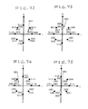
- FIG. 2 is a block diagram of a modulator (a quadrature baseband modulator) in FIG. 1 .
- FIG. 3 is a block diagram of a receiver in the radio communication system according to the first embodiment of this invention.
- FIG. 4 is a block diagram of a quasi synchronous detector in FIG. 3 .
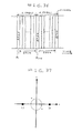
- FIG. 5 is a diagram of an arrangement of 16 signal points in an I-Q plane which are provided by 16-value APSK.
- FIG. 6 is a diagram of an arrangement of signal points in an I-Q plane which are provided by QPSK.
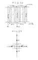
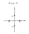
- FIG. 7 is a time-domain diagram of a symbol stream.
- FIG. 8 is a bock diagram of a modulator (a quadrature baseband modulator) in a transmitter in a radio communication system according to a second embodiment of this invention.
- FIG. 9 is a bock diagram of a quasi synchronous detector in a receiver in the radio communication system according to the second embodiment of this invention.
- FIG. 10 is a diagram of an arrangement of signal points in an I-Q plane which are provided by 2 2m QAM (2 2m -value QAM).
- FIG. 11 is a time-domain diagram of a symbol stream.
- FIG. 12 is a diagram of an arrangement of signal points in an I-Q plane which are provided by 16QAM (16-value QAM).
- FIG. 13 is a time-domain diagram of a symbol stream.
- FIG. 14 is a block diagram of a modulator (a quadrature baseband modulator) in a transmitter in a radio communication system according to a fourth embodiment of this invention.
- FIG. 15 is a diagram of an arrangement of signal points in an I-Q plane which are provided by QPSK.
- FIG. 16 is a block diagram of a quasi synchronous detector in a receiver in the radio communication system according to the fourth embodiment of this invention.
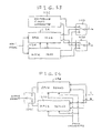
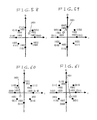
- FIG. 17 is a block diagram of a modulator (a quadrature baseband modulator) in a transmitter in a radio communication system according to a fifth embodiment of this invention.
- FIG. 18 is a block diagram of a quasi synchronous detector in a receiver in the radio communication system according to the fifth embodiment of this invention.
- FIG. 19 is a block diagram of a modulator (a quadrature baseband modulator) in a transmitter in a radio communication system according to a seventh embodiment of this invention.
- FIG. 20 is a block diagram of a quasi synchronous detector in a receiver in the radio communication system according to the seventh embodiment of this invention.
- FIG. 21 is a diagram of an arrangement of signal points in an I-Q plane which are provided by 2 2m QAM (2 2m -value QAM).
- FIG. 22 is a diagram of an arrangement of signal points in an I-Q plane which are provided by 16QAM (16-value QAM).
- FIG. 23 is a block diagram of a modulator (a quadrature baseband modulator) in a transmitter in a radio communication system according to a ninth embodiment of this invention.
- FIG. 24 is a block diagram of a quasi synchronous detector in a receiver in the radio communication system according to the ninth embodiment of this invention.
- FIG. 25 is a time-domain diagram of a symbol stream.
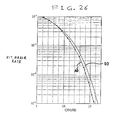
- FIG. 26 is a diagram of the relation between the bit error rate and the carrier-to-noise power ratio which is provided in an eleventh embodiment of this invention, and the corresponding relation in a prior-art system.
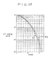
- FIG. 27 is a diagram of the relation between the bit error rate and the carrier-to-noise power ratio which is provided in a twelfth embodiment of this invention, and the corresponding relation in a prior-art system.
- FIG. 28 is a diagram of the relation between the bit error rate and the carrier-to-noise power ratio which is provided in a thirteenth embodiment of this invention, and the corresponding relation in a prior-art system.
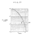
- FIG. 29 is a diagram of the relation between the bit error rate and the carrier-to-noise power ratio which is provided in a fourteenth embodiment of this invention, and the corresponding relation in a prior-art system.
- FIG. 30 is a block diagram of a transmitter in a radio communication system according to a fifteenth embodiment of this invention.
- FIG. 31 is a block diagram of a modulator (a quadrature baseband modulator) in FIG. 30 .
- FIG. 32 is a block diagram of a receiver in the radio communication system according to the fifteenth embodiment of this invention.
- FIG. 33 is a block diagram of a quasi synchronous detector in FIG. 32 .
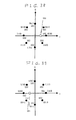
- FIG. 34 is a diagram of an arrangement of 8 signal points in an I-Q plane which are provided by 8PSK.
- FIG. 35 is a diagram of an arrangement of two signal points in an I-Q plane which are provided by BPSK.
- FIG. 36 is a time-domain diagram of a symbol stream.
- FIG. 37 is a diagram of an arrangement of signal points of BPSK, and logic states assigned thereto.
- FIG. 38 is a diagram of signal points of 8PSK, logic states assigned thereto, and a first signal point of BPSK.
- FIG. 39 is a diagram of signal points of 8PSK, logic states assigned thereto, and a second signal point of BPSK.
- FIG. 40 is a block diagram of a modulator (a quadrature baseband modulator) in a transmitter in a radio communication system according to a sixteenth embodiment of this invention.
- FIG. 41 is a block diagram of a quasi synchronous detector in a receiver in the radio communication system according to the sixteenth embodiment of this invention.
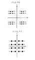
- FIG. 42 is a diagram of an arrangement of signal points in an I-Q plane which are provided by 2 2m QAM (2 2m -value QAM).
- FIG. 43 is a diagram of an arrangement of signal points in an I-Q plane which are provided by 16QAM (16-value QAM).
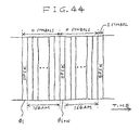
- FIG. 44 is a time-domain diagram of a symbol stream.
- FIG. 45 is a diagram of signal points of 16QAM (16-value QAM), logic states assigned thereto, and a first signal point of BPSK.
- FIG. 46 is a diagram of signal points of 16QAM (16-value QAM), logic states assigned thereto, and a second signal point of BPSK.
- FIG. 47 is a block diagram of a modulator (a quadrature baseband modulator) in a transmitter in a radio communication system according to a seventeenth embodiment of this invention.
- FIG. 48 is a block diagram of a quasi synchronous detector in a receiver in the radio communication system according to the seventeenth embodiment of this invention.
- FIG. 49 is a diagram of an arrangement of signal points in an I-Q plane which are provided by 2 2m QAM (2 2m -value QAM).
- FIG. 50 is a diagram of an arrangement of signal points in an I-Q plane which are provided by 16QAM (16-value QAM).
- FIG. 51 is a diagram of signal points of 16QAM (16-value QAM), logic states assigned thereto, and a first signal point of BPSK.
- FIG. 52 is a diagram of signal points of 16QAM (16-value QAM), logic states assigned thereto, and a second signal point of BPSK.
- FIG. 53 is a block diagram of a modulator (a quadrature baseband modulator) in a transmitter in a radio communication system according to an eighteenth embodiment of this invention.
- FIG. 54 is a block diagram of a quasi synchronous detector in a receiver in the radio communication system according to the eighteenth embodiment of this invention.
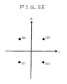
- FIG. 55 is a diagram of an arrangement of signal points in an I-Q plane which are provided by QPSK.
- FIG. 56 is a time-domain diagram of a symbol stream.
- FIG. 57 is a diagram of signal points of QPSK, and logic states assigned thereto.
- FIG. 58 is a diagram of signal points of 8PSK, logic states assigned thereto, and a first signal point of QPSK.
- FIG. 59 is a diagram of signal points of 8PSK, logic states assigned thereto, and a second signal point of QPSK.
- FIG. 60 is a diagram of signal points of 8PSK, logic states assigned thereto, and a third signal point of QPSK.
- FIG. 61 is a diagram of signal points of 8PSK, logic states assigned thereto, and a fourth signal point of QPSK.
- FIG. 62 is a block diagram of a modulator (a quadrature baseband modulator) in a transmitter in a radio communication system according to a nineteenth embodiment of this invention.
- FIG. 63 is a block diagram of a quasi synchronous detector in a receiver in the radio communication system according to the nineteenth embodiment of this invention.
- FIG. 64 is a time-domain diagram of a symbol stream.
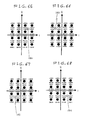
- FIG. 65 is a diagram of signal points of 16QAM (16-value QAM), logic states assigned thereto, and a first signal point of QPSK.
- FIG. 66 is a diagram of signal points of 16QAM (16-value QAM), logic states assigned thereto, and a second signal point of QPSK.
- FIG. 67 is a diagram of signal points of 16QAM (16-value QAM), logic states assigned thereto, and a third signal point of QPSK.
- FIG. 68 is a diagram of signal points of 16QAM (16-value QAM), logic states assigned thereto, and a fourth signal point of QPSK.
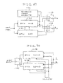
- FIG. 69 is a block diagram of a modulator (a quadrature baseband modulator) in a transmitter in a radio communication system according to a twentieth embodiment of this invention.
- FIG. 70 is a block diagram of a quasi synchronous detector in a receiver in the radio communication system according to the twentieth embodiment of this invention.
- FIG. 71 is a diagram of an arrangement of signal points in an I-Q plane which are provided by QPSK.
- FIG. 72 is a diagram of signal points of 8PSK, logic states assigned thereto, and a first signal point of QPSK.
- FIG. 73 is a diagram of signal points of 8PSK, logic states assigned thereto, and a second signal point of QPSK.
- FIG. 74 is a diagram of signal points of 8PSK, logic states assigned thereto, and a third signal point of QPSK.
- FIG. 75 is a diagram of signal points of 8PSK, logic states assigned thereto, and a fourth signal point of QPSK.
- FIG. 76 is a block diagram of a modulator (a quadrature baseband modulator) in a transmitter in a radio communication system according to a twenty-first embodiment of this invention.
- FIG. 77 is a block diagram of a quasi synchronous detector in a receiver in the radio communication system according to the twenty-first embodiment of this invention.
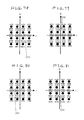
- FIG. 78 is a diagram of signal points of 16QAM (16-value QAM), logic states assigned thereto, and a first signal point of QPSK.
- FIG. 79 is a diagram of signal points of 16QAM (16-value QAM), logic states assigned thereto, and a second signal point of QPSK.
- FIG. 80 is a diagram of signal points of 16QAM (16-value QAM), logic states assigned thereto, and a third signal point of QPSK.
- FIG. 81 is a diagram of signal points of 16QAM (16-value QAM), logic states assigned thereto, and a fourth signal point of QPSK.
- FIG. 82 is a block diagram of a modulator (a quadrature baseband modulator) in a transmitter in a radio communication system according to a twenty-second embodiment of this invention.
- FIG. 83 is a block diagram of a quasi synchronous detector in a receiver in the radio communication system according to the twenty-second embodiment of this invention.
- FIG. 84 is a diagram of signal points of 16QAM (16-value QAM), logic states assigned thereto, and a first signal point of QPSK.
- FIG. 85 is a diagram of signal points of 16QAM (16-value QAM), logic states assigned thereto, and a second signal point of QPSK.
- FIG. 86 is a diagram of signal points of 16QAM (16-value QAM), logic states assigned thereto, and a third signal point of QPSK.
- FIG. 87 is a diagram of signal points of 16QAM (16-value QAM), logic states assigned thereto, and a fourth signal point of QPSK.
- FIG. 88 is a block diagram of a modulator (a quadrature baseband modulator) in a transmitter in a radio communication system according to a twenty-third embodiment of this invention.
- FIG. 89 is a block diagram of a quasi synchronous detector in a receiver in the radio communication system according to the twenty-third embodiment of this invention.
- FIG. 90 is a diagram of signal points of 16QAM (16-value QAM), logic states assigned thereto, and a first signal point of QPSK.
- FIG. 91 is a diagram of signal points of 16QAM (16-value QAM), logic states assigned thereto, and a second signal point of QPSK.
- FIG. 92 is a diagram of signal points of 16QAM (16-value QAM), logic states assigned thereto, and a third signal point of QPSK.
- FIG. 93 is a diagram of signal points of 16QAM (16-value QAM), logic states assigned thereto, and a fourth signal point of QPSK.
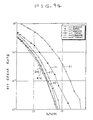
- FIG. 94 is a diagram of relations between the bit error rate and the ratio of the 1-bit signal energy “Eb” to the noise power density “N 0 ”.
- 2 2m -value QAM means 2 2m QAM
- 16-value QAM means 16QAM and 16-value APSK means 16APSK.
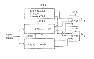
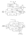
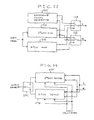
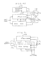
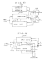
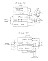
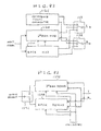
- FIG. 1 shows a transmitter 10 in a radio communication system according to a first embodiment of this invention.
- the transmitter 10 includes a modulator 12 and an RF (radio frequency) portion 15 .
- the modulator 12 is defined and referred to as the quadrature baseband modulator 12 .
- a digital signal to be transmitted (that is, an input digital signal or main information to be transmitted) is fed to the quadrature baseband modulator 12 .
- the device 12 subjects the input digital signal to quadrature baseband modulation, thereby converting the input digital signal into a pair of modulation-resultant baseband signals, that is, a baseband I (in-phase) signal and a baseband Q (quadrature) signal.
- the quadrature baseband modulator 12 outputs the baseband I signal and the baseband Q signal to the RF portion 15 .
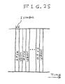
- a pair of modulated baseband I and Q signals is composed of (or contains) a stream of modulated symbols.
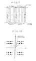
- the quadrature baseband modulator 12 outputs the baseband I and Q signals composed of a stream of modulated symbols as shown in FIG. 7 .
- FIG. 7 shows an arrangement of a symbol stream according to the base concept of the invention.
- the symbol stream is basically composed of first symbols having been subjected to a first modulation scheme (16 APSK in the specific example of FIG. 7 ) and periodically includes second symbols having been subjected to a second modulation scheme (QPSK in the specific example of FIG. 7 ) which is different from the first modulation scheme.
- each of the second symbols as a pilot symbol from which the amplitude distortion and the phase distortion can be estimated for use in demodulation of the second symbols following the first symbol.
- Many widely different embodiments of the quadrature baseband modulator 12 can be constructed. Some embodiments will be described in the followings.
- the RF portion 15 converts the baseband I signal and the baseband Q signal into an RF signal through frequency conversion which may include RF modulation.
- the RF portion 15 feeds the RF signal to an antenna 17 .
- the RF signal is radiated by the antenna 17 .
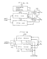
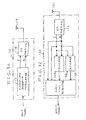
- the quadrature baseband modulator 12 includes a 16-value APSK (amplitude phase shift keying) modulator 12 A, a QPSK (quadrature phase shift keying) modulator 12 B, a reference signal generator 12 C, and switches 12 D and 12 E.
- APSK amplitude phase shift keying
- QPSK quadrature phase shift keying
- the APSK modulator 12 A and the QPSK modulator 12 B receives the input digital signal.
- the device 12 A subjects the input digital signal to 16APSK (16-value APSK modulation), thereby converting the input digital signal into a pair of a baseband I signal and a baseband Q signal.
- the APSK modulator 12 A outputs the baseband I signal to the switch 12 D.
- the APSK modulator 12 A outputs the baseband Q signal to the switch 12 E.
- the device 12 B subjects the input digital signal to QPSK (QPSK modulation), thereby converting the input digital signal into a pair of a baseband I signal and a baseband Q signal.
- the QPSK modulator 12 B outputs the baseband I signal to the switch 12 D.
- the QPSK modulator 12 B outputs the baseband Q signal to the switch 12 E.
- the reference signal generator 12 C outputs a reference baseband I signal to the switch 12 D.
- the reference signal generator 12 C outputs a reference baseband Q signal to the switch 12 E.
- the output I and Q signals from the reference signal generator 12 C are used in acquiring synchronization between the transmitter 10 and a receiver during an initial stage of signal transmission.
- the switch 12 D selects one of the output I signal from the APSK modulator 12 A, the output I signal from the QPSK modulator 12 B, and the output I signal from the reference signal generator 12 C, and transmits the selected I signal to the RF portion 15 .
- the switch 12 E selects one of the output Q signal from the APSK modulator 12 A, the output Q signal from the QPSK modulator 12 B, and the output Q signal from the reference signal generator 12 C, and transmits the selected Q signal to the RF portion 15 .
- the switch 12 D selects the output I signal from the reference signal generator 12 C while the switch 12 E selects the output Q signal from the reference signal generator 12 C.
- the switch 12 D alternately selects one of the output I signal from the APSK modulator 12 A and the output I signal from the QPSK modulator 12 B at a predetermined period, and transmits the selected I signal to the RF portion 15 .
- the switch 12 E alternately selects one of the output Q signal from the APSK modulator 12 A and the output Q signal from the QPSK modulator 12 B at the predetermined period, and transmits the selected Q signal to the RF portion 15 .
- the quadrature baseband modulator 12 alternately implements the 16-value APSK modulation and the QPSK modulation at the predetermined period.
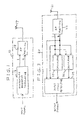
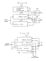
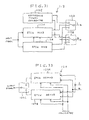
- FIG. 3 shows a receiver 20 in the radio communication system according to the first embodiment of this invention.
- the receiver 20 includes an RF portion 22 , calculators 25 and 26 , and a quasi synchronous detector 29 .
- An RF signal caught by an antenna 21 is applied to the RF portion 22 .
- the RF portion 22 subjects the applied RF signal to frequency conversion (which may include RF demodulation), thereby converting the applied RF signal into a pair of a baseband I signal and a baseband Q signal.
- the RF portion 22 outputs the baseband I signal and the baseband Q signal to the calculators 25 and 26 , and the quasi synchronous detector 29 .
- the calculator 25 estimates an amplitude distortion amount from the baseband I signal and the baseband Q signal.
- the calculator 25 informs the quasi synchronous detector 29 of the estimated amplitude distortion amount.
- the calculator 26 estimates a frequency offset amount from the baseband I signal and the baseband Q signal.
- the calculator 26 informs the quasi synchronous detector 29 of the estimated frequency offset amount.
- the device 29 subjects the baseband I signal and the baseband Q signal to quasi synchronous detection responsive to the estimated amplitude distortion amount and the estimated frequency offset amount, thereby demodulating the baseband I signal and the baseband Q signal into an original digital signal.
- the quasi synchronous detector 29 recovers the original digital signal from the baseband I signal and the baseband Q signal.
- the quasi synchronous detector 29 outputs the recovered original digital signal.
- the quasi synchronous detector 29 includes a 16-value APSK demodulator 29 A, a QPSK demodulator 29 B, and a switch 29 C.
- the APSK demodulator 29 A and the QPSK demodulator 29 B receive the baseband I and Q signals from the RF portion 22 .
- the APSK demodulator 29 A and the QPSK demodulator 29 B are informed of the estimated amplitude distortion amount and the estimated frequency offset amount by the calculators 25 and 26 .
- the device 29 A subjects the baseband I signal and the baseband Q signal to 16-value APSK demodulation responsive to the estimated amplitude distortion amount and the estimated frequency offset amount, thereby demodulating the baseband I signal and the baseband Q signal into an original digital signal.
- the APSK demodulator 29 A recovers the original digital signal from the baseband I signal and the baseband Q signal.
- the APSK demodulator 29 A outputs the recovered original digital signal to the switch 29 C.
- the device 29 B subjects the baseband I signal and the baseband Q signal to QPSK demodulation responsive to the estimated amplitude distortion amount and the estimated frequency offset amount, thereby demodulating the baseband I signal and the baseband Q signal into an original digital signal.
- the QPSK demodulator 29 B recovers the original digital signal from the baseband I signal and the baseband Q signal.
- the QPSK demodulator 29 B outputs the recovered original digital signal to the switch 29 C.
- the switch 29 C alternately selects the output digital signal from the APSK demodulator 29 A and the output digital signal from the QPSK demodulator 29 B in response to a timing signal (a frame and symbol sync signal), and transmits the selected digital signal to a later stage.
- a timing signal a frame and symbol sync signal
- the switch 29 C selects the output digital signal from the APSK demodulator 29 A.
- the switch 29 C selects the output digital signal from the QPSK demodulator 29 B.
- the APSK demodulator 29 A includes an amplitude correction circuit (an amplitude compensation circuit) and a frequency correction circuit (a frequency compensation circuit).
- the amplitude correction circuit compensates for an amplitude distortion of the baseband I signal and the baseband Q signal in response to the estimated amplitude distortion, thereby generating a first compensation-resultant baseband I signal and a first compensation-resultant baseband Q signal.
- the frequency correction circuit compensates for a frequency offset of the first compensation-resultant baseband I signal and the first compensation-resultant baseband Q signal in response to the estimated frequency offset amount, thereby generating a second compensation-resultant baseband I signal and a second compensation-resultant baseband Q signal.
- the second compensation-resultant baseband I signal and the second compensation-resultant baseband Q signal are subjected to the 16-value APSK demodulation, being converted into the original digital signal.
- the QPSK demodulator 29 B includes an amplitude correction circuit and a frequency correction circuit.
- the amplitude correction circuit compensates for an amplitude distortion of the baseband I signal and the baseband Q signal in response to the estimated amplitude distortion, thereby generating a first compensation-resultant baseband I signal and a first compensation-resultant baseband Q signal.
- the frequency correction circuit compensates for a frequency offset of the first compensation-resultant baseband I signal and the first compensation-resultant baseband Q signal in response to the estimated frequency offset amount, thereby generating a second compensation-resultant baseband I signal and a second compensation-resultant baseband Q signal.
- the second compensation-resultant baseband I signal and the second compensation-resultant baseband Q signal are subjected to the QPSK demodulation, being converted into the original digital signal.
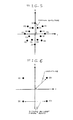
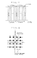
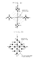
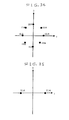
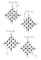
- FIG. 5 shows an arrangement of 16 signal points in an I-Q plane which are provided by the 16-value APSK modulation.
- the 16 signal points are denoted by the reference numeral “ 101 ”.
- the 16 signal points are assigned to 16 different logic values respectively.
- the positions (I 16APSK , Q 16APSK ) of the 16 signal points are given by the following equations.
- I 16 ⁇ APSK h ⁇ 0 ⁇ ⁇ cos ⁇ ( ⁇ 8 ) ⁇ cos ⁇ ( k ⁇ ⁇ 4 ) - sin ⁇ ( ⁇ 8 ) ⁇ sin ⁇ ( k ⁇ ⁇ 4 ) ⁇ + h ⁇ 1 ⁇ ⁇ cos ⁇ ( k ⁇ ⁇ 4 ) ( 1 )
- Q 16 ⁇ APSK h ⁇ 0 ⁇ ⁇ cos ⁇ ( ⁇ 8 ) ⁇ cos ⁇ ( k ⁇ ⁇ 4 ) + sin ⁇ ( ⁇ 8 ) ⁇ cos ⁇ ( k ⁇ ⁇ 4 ) ⁇ + h ⁇ 1 ⁇ ⁇ sin ⁇ ( k ⁇ ⁇ 4 ) ( 2 )
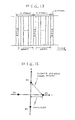
- FIG. 6 shows an arrangement of signal points in an I-Q plane which are provided by the QPSK modulation.
- the signal points are denoted by the reference numeral “ 201 ”.
- the signal points are assigned to different logic values respectively.
- the positions (I QPSK , Q QPSK ) of the signal points are given by the following equations.
- I Q ⁇ PSK p ⁇ ⁇ cos ⁇ ( ⁇ 4 ) ⁇ cos ⁇ ( k ⁇ ⁇ 2 ) - sin ⁇ ( ⁇ 4 ) ⁇ sin ⁇ ( k ⁇ ⁇ 2 ) ⁇ ( 3 )
- Q Q ⁇ PSK p ⁇ ⁇ cos ⁇ ( ⁇ 4 ) ⁇ sin ⁇ ( k ⁇ ⁇ 2 ) + sin ⁇ ( ⁇ 4 ) ⁇ cos ⁇ ( k ⁇ ⁇ 2 ) ⁇ ( 4 )
- k denotes a variable integer
- p denotes a predetermined constant.
- all the signal points correspond to a same amplitude given by the constant “p”.
- all the distances between the neighboring signal points are equal to a same value given by ⁇ square root over (2p) ⁇ .
- the signal points are spaced at equal angular intervals. Accordingly, a QPSK modulation-resultant signal is suited for detecting an amplitude distortion and a frequency offset.
- a pair of the I signal and the Q signal outputted from the quadrature baseband modulator 12 in the transmitter 10 , or the RF signal outputted from the RF portion 15 in the transmitter 10 is composed of a stream of frames each having N successive symbols.
- N denotes a predetermined natural number.
- the first symbol results from the QPSK modulation
- the second and later symbols result from the 16-value APSK modulation.
- the first symbol in every frame (that is, the QPSK symbol in every frame) is used by the receiver 20 as a pilot symbol for estimating an amplitude distortion amount and a frequency offset amount. It should be noted that every pilot symbol also carries a part of the main information to be transmitted.
- the calculator 25 separates pilot symbols (first symbols in frames) from the output I and Q signals of the RF portion 22 in response to a signal (a frame and symbol sync signal) having a period corresponding to N symbols.
- the calculator 25 estimates an amplitude distortion amount from the separated pilot symbols.
- the calculator 26 separates pilot symbols (first symbols in frames) from the output I and Q signals of the RF portion 22 in response to a signal (a frame and symbol sync signal) having a period corresponding to N symbols.
- the calculator 26 estimates a frequency offset amount from the separated pilot symbols.
- the maximum amplitude g 1 provided by the 16-value APSK modulation is equal to the amplitude “p” provided by the QPSK modulation.
- the amplitude distortion amount and the frequency offset amount can be accurately estimated.
- the quasi synchronous detector 29 in the receiver 20 is designed to implement the following processes.
- the quasi synchronous detector 29 subjects the output I and Q signals of the RF portion 22 to the QPSK demodulation and outputs the QPSK-demodulation-resultant digital signal when the output I and Q signals of the RF portion 22 represent a pilot symbol.
- the quasi synchronous detector 29 subjects the output I and Q signals of the RF portion 22 to the 16-value APSK demodulation and outputs the APSK-demodulation-resultant digital signal when the output I and Q signals of the RF portion 22 represent a normal symbol different from a pilot symbol.
- a second embodiment of this invention is similar to the first embodiment thereof except for design changes indicated hereinafter.
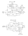
- a modulator (a quadrature baseband modulator) in a transmitter in the second embodiment of this invention includes a 2 2m QAM (2 2m -value QAM or 2 2m -value quadrature amplitude modulation) modulator 12 F instead of the 16-value APSK modulator 12 A (see FIG. 2 ).
- “m” denotes a predetermined integer equal to or greater than “2”.
- a quasi synchronous detector in a receiver in the second embodiment of this invention includes a 2 2m -value QAM demodulator 29 D instead of the 16-value APSK demodulator 29 A (see FIG. 4 ).
- FIG. 10 shows an arrangement of signal points in an I-Q plane which are provided by 2 2m -value QAM executed in the QAM modulator 12 F.
- the signal points are denoted by the reference numeral “ 401 ”.
- the signal points are assigned to different logic values respectively.
- the positions (I QAM , Q QAM ) of the signal points are given by the following equations.
- I QAM q(2 m ⁇ 1 a 1 + 2 m ⁇ 2 a 2 + . . . + 2 0 am)
- Q QAM q(2 m ⁇ 1 b 1 + 2 m ⁇ 2 b 2 + . . .
- a pair of the I signal and the Q signal outputted from the quadrature baseband modulator in the transmitter (see FIG. 1 ), or the RF signal outputted from the RF portion in the transmitter is composed of a stream of frames each having N successive symbols.
- N denotes a predetermined natural number.
- the first symbol results from the QPSK modulation, and the second and later symbols result from the 2 2m -value QAM.
- the first symbol in every frame (that is, the QPSK symbol in every frame) is used by the receiver as a pilot symbol for estimating an amplitude distortion amount and a frequency offset amount. It should be noted that every pilot symbol also carries a part of the main information to be transmitted.
- the calculator 25 separates pilot symbols (first symbols in frames) from the output I and Q signals of the RF portion 22 in response to a signal (a frame and symbol sync signal) having a period corresponding to N symbols.
- the calculator 25 estimates an amplitude distortion amount from the separated pilot symbols.
- the calculator 26 separates pilot symbols (first symbols in frames) from the output I and Q signals of the RF portion 22 in response to a signal (a frame and symbol sync signal) having a period corresponding to N symbols.
- the calculator 26 estimates a frequency offset amount from the separated pilot symbols.
- the maximum amplitude provided by the 2 2m -value QAM that is, the value given by the expression (7), is equal to the amplitude “p” provided by the QPSK modulation.
- the amplitude distortion amount and the frequency offset amount can be accurately estimated.
- the quasi synchronous detector 29 in the receiver (see FIG. 3 ) is designed to implement the following processes.
- the quasi synchronous detector 29 subjects the output I and Q signals of the RF portion 22 to QPSK demodulation and outputs the QPSK-demodulation-resultant digital signal when the output I and Q signals of the RF portion 22 represent a pilot symbol.
- the quasi synchronous detector 29 subjects the output I and Q signals of the RF portion 22 to 2 2m -value QAM demodulation and outputs the QAM-demodulation-resultant digital signal when the output I and Q signals of the RF portion 22 represent a normal symbol different from a pilot symbol.
- a third embodiment of this invention is similar to the second embodiment thereof except that 16-value QAM replaces 2 2m -value QAM.
- a modulator (a quadrature baseband modulator) in a transmitter includes a 16-value QAM modulator instead of the 2 2m -value QAM modulator 12 F (see FIG. 8 ).
- a quasi synchronous detector in a receiver includes a 16-value QAM demodulator instead of the 2 2m -value QAM demodulator 29 D (see FIG. 9 ).
- FIG. 12 shows an arrangement of signal points in an I-Q plane which are provided by the 16-value QAM.
- the signal points are denoted by the reference numeral “ 601 ”.
- the signal points are assigned to different logic values respectively.
- the positions (I 16QAM , Q 16QAM ) of the signal points are given by the following equations.
- I 16QAM r(2 1 a+ 2 0 a 2 )
- Q 16QAM r(2 1 b 1 + 2 0 b 2 (9) where (a 1 , b 1 ) and (a 2 , b 2 ) are binary code words of “1” and “ 31 1”, and “r” denotes a predetermined constant.
- specified ones of the signal points correspond to the maximum amplitude which is given as follows. (2 1 +2 0 ) ⁇ square root over (2) ⁇ r (10) In addition, the distances between the neighboring signal points are equal to a same value given by “2r”.
- a pair of the I signal and the Q signal outputted from the quadrature baseband modulator in the transmitter (see FIG. 1 ), or the RF signal outputted from the RF portion in the transmitter is composed of a stream of frames each having N successive symbols.
- N denotes a predetermined natural number.
- the first symbol results from the QPSK modulation, and the second and later symbols result from the 16-value QAM.
- the first symbol in every frame (that is, the QPSK symbol in every frame) is used by the receiver as a pilot symbol for estimating an amplitude distortion amount and a frequency offset amount. It should be noted that every pilot symbol also carries a part of the main information to be transmitted.
- the calculator 25 separates pilot symbols (first symbols in frames) from the output I and Q signals of the RF portion 22 in response to a signal (a frame and symbol sync signal) having a period corresponding to N symbols.
- the calculator 25 estimates an amplitude distortion amount from the separated pilot symbols.
- the calculator 26 separates pilot symbols (first symbols in frames) from the output I and Q signals of the RF portion 22 in response to a signal (a frame and symbol sync signal) having a period corresponding to N symbols.
- the calculator 26 estimates a frequency offset amount from the separated pilot symbols.
- the maximum amplitude provided by the 16-value QAM that is, the value given by the expression (10) is equal to the amplitude “p” provided by the QPSK modulation.
- the amplitude distortion amount and the frequency offset amount can be accurately estimated.
- the quasi synchronous detector 29 in the receiver (see FIG. 3 ) is designed to implement the following processes.
- the quasi synchronous detector 29 subjects the output I and Q signals of the RF portion 22 to QPSK demodulation and outputs the QPSK-demodulation-resultant digital signal when the output I and Q signals of the RF portion 22 represent a pilot symbol.
- the quasi synchronous detector 29 subjects the output I and Q signals of the RF portion 22 to 16-value QAM demodulation and the QAM-demodulation-resultant digital signal when the output I and Q signals of the RF portion 22 represent a normal symbol different from a pilot symbol.
- the inter-signal-point distance “ ⁇ square root over (2p”) ⁇ in the QPSK modulation is equal to a given value times the inter-signal-point distance “2r” in the 16-value QAM.
- the given value is in the range of 0.90 to 1.50. In this case, a sufficiently low bit error rate is provided.
- the inter-signal-point distance “ ⁇ square root over (2p”) ⁇ in the QPSK modulation may be equal to twice the inter-signal-point distance “2r” in the 16-value QAM.
- the quasi synchronous detector in the receiver detects the I-Q-plane amplitude of the output I and Q signals of the RF portion when the output I and Q signals of the RF portion 22 represent a pilot symbol, and that the detected I-Q-plane amplitude is used as an I-Q-plane amplitude threshold value for the 16-value QAM demodulation.
- a fourth embodiment of this invention is similar to the first embodiment thereof except for design changes indicated hereinafter.
- a modulator (a quadrature baseband modulator) in a transmitter in the fourth embodiment of this invention includes a QPSK modulator 12 G instead of the QPSK modulator 12 B (see FIG. 2 ).
- FIG. 15 shows an arrangement of signal points in an I-Q plane which are provided by QPSK modulation implemented by the QPSK modulator 12 G.
- the signal points are denoted by the reference numeral “ 801 ”.
- the signal points are assigned to different logic values respectively.
- the positions (I QPSKR , Q QPSKR ) of the signal points are given by the following equations.
- I Q ⁇ PSKR I Q ⁇ PSK ⁇ ⁇ cos ⁇ ( ⁇ 4 + n ⁇ ⁇ 2 ) ⁇ - Q Q ⁇ PSK ⁇ ⁇ sin ⁇ ( ⁇ 4 + n ⁇ ⁇ 2 ) ⁇ ( 11 )
- Q Q ⁇ PSKR I Q ⁇ PSK ⁇ ⁇ sin ⁇ ( ⁇ 4 + n ⁇ ⁇ 2 ) ⁇ ⁇ Q Q ⁇ PSK ⁇ ⁇ cos ⁇ ( ⁇ 4 + n ⁇ ⁇ 2 ) ⁇ ( 12 )
- n denotes an integer
- (I QPSK , Q QPSK ) are given by the equations (3) and (4).
- all the signal points correspond to a same amplitude given by the constant “p”.
- all the distances between the neighboring signal points are equal to a same value given by ⁇ square root over (2p) ⁇ .
- the signal points are spaced at equal angular intervals. Accordingly, a QPSK modulation-resultant signal is suited for detecting an amplitude distortion and a frequency offset.
- a quasi synchronous detector in a receiver in the fourth embodiment of this invention includes a QPSK demodulator 29 E instead of the QPSK demodulator 29 B (see FIG. 4 ).
- the QPSK demodulator 29 E implements demodulation inverse with respect to the modulation by the QPSK modulator 12 G.
- a pair of the I signal and the Q signal outputted from the quadrature baseband modulator 12 in the transmitter 10 (see FIG. 1 ), or the RF signal outputted from the RF portion 15 in the transmitter 10 is composed of a stream of frames each having N successive symbols.
- N denotes a predetermined natural number.
- the first symbol results from the QPSK modulation
- the second and later symbols result from the 16-value APSK modulation.
- the first symbol in every frame (that is, the QPSK symbol in every frame) is used by the receiver 20 (see FIG. 3 ) as a pilot symbol for estimating an amplitude distortion amount and a frequency offset amount. It should be noted that every pilot symbol also carries a part of the main information to be transmitted.
- the calculator 25 separates pilot symbols (first symbols in frames) from the output I and Q signals of the RF portion 22 in response to a signal (a frame and symbol sync signal) having a period corresponding to N symbols.
- the calculator 25 estimates an amplitude distortion amount from the separated pilot symbols.
- the calculator 26 separates pilot symbols (first symbols in frames) from the output I and Q signals of the RF portion 22 in response to a signal (a frame and symbol sync signal) having a period corresponding to N symbols.
- the calculator 26 estimates a frequency offset amount from the separated pilot symbols.
- the maximum amplitude g 1 provided by the 16-value APSK modulation is equal to the amplitude “p” provided by the QPSK modulation.
- the amplitude distortion amount and the frequency offset amount can be accurately estimated.
- the quasi synchronous detector 29 in the receiver 20 is designed to implement the following processes.
- the quasi synchronous detector 29 subjects the output I and Q signals of the RF portion 22 to the QPSK demodulation and outputs the QPSK-demodulation-resultant digital signal when the output I and Q signals of the RF portion 22 represent a pilot symbol.
- the quasi synchronous detector 29 subjects the output I and Q signals of the RF portion 22 to the 16-value APSK demodulation and outputs the APSK-demodulation-resultant digital signal when the output I and Q signals of the RF portion 22 represent a normal symbol different from a pilot symbol.
- a fifth embodiment of this invention is similar to the second embodiment thereof except for design changes indicated hereinafter.
- a modulator in a transmitter in the fifth embodiment of this invention includes a QPSK modulator 12 G instead of the QPSK modulator 12 B (see FIG. 8 ).
- the QPSK modulator 12 G implements QPSK modulation providing signal points which are arranged in an I-Q plane as shown in FIG. 15 .
- a quasi synchronous detector in a receiver in the fifth embodiment of this invention includes a QPSK demodulator 29 E instead of the QPSK demodulator 29 B (see FIG. 9 ).
- the QPSK demodulator 29 E implements demodulation inverse with respect to the modulation by the QPSK modulator 12 G.
- a pair of the I signal and the Q signal outputted from the quadrature baseband modulator in the transmitter (see FIG. 1 ), or the RF signal outputted from the RF portion in the transmitter is composed of a stream of frames each having N successive symbols.
- N denotes a predetermined natural number.
- the first symbol results from the QPSK modulation, and the second and later symbols result from the 2 2m -value QAM.
- the first symbol in every frame (that is, the QPSK symbol in every frame) is used by the receiver as a pilot symbol for estimating an amplitude distortion amount and a frequency offset amount. It should be noted that every pilot symbol also carries a part of the main information to be transmitted.
- the calculator 25 separates pilot symbols (first symbols in frames) from the output I and Q signals of the RF portion 22 in response to a signal (a frame and symbol sync signal) having a period corresponding to N symbols.
- the calculator 25 estimates an amplitude distortion amount from the separated pilot symbols.
- the calculator 26 separates pilot symbols (first symbols in frames) from the output I and Q signals of the RF portion 22 in response to a signal (a frame and symbol sync signal) having a period corresponding to N symbols.
- the calculator 26 estimates a frequency offset amount from the separated pilot symbols.
- the maximum amplitude provided by the 2 2m -value QAM that is, the value given by the expression (7), is equal to the amplitude “p” provided by the QPSK modulation.
- the amplitude distortion amount and the frequency offset amount can be accurately estimated.
- the quasi synchronous detector 29 in the receiver (see FIG. 3 ) is designed to implement the following processes.
- the quasi synchronous detector 29 subjects the output I and Q signals of the RF portion 22 to QPSK demodulation and outputs the QPSK-demodulation-resultant digital signal when the output I and Q signals of the RF portion 22 represent a pilot symbol.
- the quasi synchronous detector 29 subjects the output I and Q signals of the RF portion 22 to 2 2m -value QAM demodulation and outputs the QAM-demodulation-resultant digital signal when the output I and Q signals of the RF portion 22 represent a normal symbol different from a pilot symbol.
- a sixth embodiment of this invention is similar to the fifth embodiment thereof except that 16-value QAM replaces 2 2m -value QAM.
- a modulator (a quadrature baseband modulator) in a transmitter includes a 16-value QAM modulator instead of the 2 2m -value QAM modulator 12 F (see FIG. 17 ).
- the QAM modulator implements 16-value QAM providing signal points which are arranged in an I-Q plane as shown in FIG. 12 .
- a quasi synchronous detector in a receiver includes a 16-value QAM demodulator instead of the 2 2m -value QAM demodulator 29 D (see FIG. 18 ).
- a pair of the I signal and the Q signal outputted from the quadrature baseband modulator in the transmitter (see FIG. 1 ), or the RF signal outputted from the RF portion in the transmitter is composed of a stream of frames each having N successive symbols.
- N denotes a predetermined natural number.
- the first symbol results from the QPSK modulation, and the second and later symbols result from the 16-value QAM.
- the first symbol in every frame (that is, the QPSK symbol in every frame) is used by the receiver as a pilot symbol for estimating an amplitude distortion amount and a frequency offset amount. It should be noted that every pilot symbol also carries a part of the main information to be transmitted.
- the calculator 25 separates pilot symbols (first symbols in frames) from the output I and Q signals of the RF portion 22 in response to a signal (a frame and symbol sync signal) having a period corresponding to N symbols.
- the calculator 25 estimates an amplitude distortion amount from the separated pilot symbols.
- the calculator 26 separates pilot symbols (first symbols in frames) from the output I and Q signals of the RF portion 22 in response to a signal (a frame and symbol sync signal) having a period corresponding to N symbols.
- the calculator 26 estimates a frequency offset amount from the separated pilot symbols.
- the maximum amplitude provided by the 16-value QAM that is, the value given by the expression (10) is equal to the amplitude “p” provided by the QPSK modulation.
- the amplitude distortion amount and the frequency offset amount can be accurately estimated.
- the quasi synchronous detector 29 in the receiver (see FIG. 3 ) is designed to implement the following processes.
- the quasi synchronous detector 29 subjects the output I and Q signals of the RF portion 22 to QPSK demodulation and outputs the QPSK-demodulation-resultant digital signal when the output I and Q signals of the RF portion 22 represent a pilot symbol.
- the quasi synchronous detector 29 subjects the output I and Q signals of the RF portion 22 to 16-value QAM demodulation and the QAM-demodulation-resultant digital signal when the output I and Q signals of the RF portion 22 represent a normal symbol different from a pilot symbol.
- the inter-signal-point distance “ ⁇ square root over (2p”) ⁇ in the QPSK modulation is equal to a given value times the inter-signal-point distance “2r” in the 16-value QAM.
- the given value is in the range of 0.90 to 1.50. In this case, a sufficiently low bit error rate is provided.
- the inter-signal-point distance “ ⁇ square root over (2p”) ⁇ in the QPSK modulation may be equal to twice the inter-signal-point distance “2r” in the 16-value QAM.
- the quasi synchronous detector in the receiver detects the I-Q-plane amplitude of the output I and Q signals of the RF portion when the output I and Q signals of the RF portion 22 represent a pilot symbol, and that the detected I-Q-plane amplitude is used as an I-Q-plane amplitude threshold value for the 16-value QAM demodulation.
- a seventh embodiment of this invention is similar to the first embodiment thereof except for design changes indicated hereinafter.
- a modulator (a quadrature baseband modulator) in a transmitter in the seventh embodiment of this invention includes a 2 2m -value QAM modulator 12 H instead of the 16-value APSK modulator 12 A (see FIG. 2 ).
- m denotes a predetermined integer equal to or greater than “2”.
- a quasi synchronous detector in a receiver in the seventh embodiment of this invention includes a 2 2m -value QAM demodulator 29 F instead of the 16-value APSK demodulator 29 A (see FIG. 4 ).
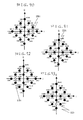
- FIG. 21 shows an arrangement of signal points in an I-Q plane which are provided by 2 2m -value QAM executed in the QAM modulator 12 H.
- the signal points are denoted by the reference numeral “ 901 ”.
- the signal points are assigned to different logic values respectively.
- the positions of the signal points in FIG. 21 result from rotation of the signal points in FIG. 10 through an angle of ⁇ /4 radian about the origin. Specifically, the positions (I QAMR , Q QAMR ) of the signal points in FIG. 21 are given by the following equations.
- I Q ⁇ AMR I Q ⁇ AM ⁇ ⁇ cos ⁇ ( ⁇ 4 + n ⁇ ⁇ 2 ) ⁇ - Q Q ⁇ A ⁇ M ⁇ ⁇ sin ⁇ ( ⁇ 4 + n ⁇ ⁇ 2 ) ⁇ ( 13 )
- Q QAMR I QAM ⁇ ⁇ sin ⁇ ( ⁇ 4 + n ⁇ ⁇ 2 ) ⁇ + Q QAM ⁇ ⁇ cos ⁇ ( ⁇ 4 + n ⁇ ⁇ 2 ) ⁇ ( 14 )
- n denotes an integer
- (I QAM , Q QAM ) are given by the equations (5) and (6).
- the maximum amplitude which corresponds to specified ones of the signal points is equal to the value given by the expression (7).
- a pair of the I signal and the Q signal outputted from the quadrature baseband modulator in the transmitter (see FIG. 1 ), or the RF signal outputted from the RF portion in the transmitter is composed of a stream of frames each having N successive symbols.
- N denotes a predetermined natural number.
- the first symbol results from the QPSK modulation, and the second and later symbols result from the 2 2m -value QAM.
- the first symbol in every frame (that is, the QPSK symbol in every frame) is used by the receiver as a pilot symbol for estimating an amplitude distortion amount and a frequency offset amount. It should be noted that every pilot symbol also carries a part of the main information to be transmitted.
- the calculator 25 separates pilot symbols (first symbols in frames) from the output I and Q signals of the RF portion 22 in response to a signal (a frame and symbol sync signal) having a period corresponding to N symbols.
- the calculator 25 estimates an amplitude distortion amount from the separated pilot symbols.
- the calculator 26 separates pilot symbols (first symbols in frames) from the output I and Q signals of the RF portion 22 in response to a signal (a frame and symbol sync signal) having a period corresponding to N symbols.
- the calculator 26 estimates a frequency offset amount from the separated pilot symbols.
- the maximum amplitude provided by the 2 2m -value QAM that is, the value given by the expression (7), is equal to the amplitude “p” provided by the QPSK modulation.
- the amplitude distortion amount and the frequency offset amount can be accurately estimated.
- the quasi synchronous detector 29 in the receiver (see FIG. 3 ) is designed to implement the following processes.
- the quasi synchronous detector 29 subjects the output I and Q signals of the RF portion 22 to QPSK demodulation and outputs the QPSK-demodulation-resultant digital signal when the output I and Q signals of the RF portion 22 represent a pilot symbol.
- the quasi synchronous detector 29 subjects the output I and Q signals of the RF portion 22 to 2 2m -value QAM demodulation and outputs the QAM-demodulation-resultant digital signal when the output I and Q signals of the RF portion 22 represent a normal symbol different from a pilot symbol.
- An eighth embodiment of this invention is similar to the seventh embodiment thereof except that 16-value QAM replaces 2 2m -value QAM.
- a modulator (a quadrature baseband modulator) in a transmitter includes a 16-value QAM modulator instead of the 2 2m -value QAM modulator 12 H (see FIG. 19 ).
- a quasi synchronous detector in a receiver includes a 16-value QAM demodulator instead of the 2 2m -value QAM demodulator 29 F (see FIG. 20 ).
- FIG. 22 shows an arrangement of signal points in an I-Q plane which are provided by 16-value QAM executed in the 16-value QAM modulator.
- the signal points are denoted by the reference numeral “ 1001 ”.
- the signal points are assigned to different logic values respectively.
- the positions of the signal points in FIG. 22 result from rotation of the signal points in FIG. 12 through an angle of ⁇ /4 radian about the origin. Specifically, the positions (I 16QAMR , Q 16QAMR ) of the signal points in FIG. 22 are given by the following equations.
- I 16 ⁇ QAMR I 16 ⁇ QAM ⁇ ⁇ cos ⁇ ( ⁇ 4 + n ⁇ ⁇ 2 ) ⁇ - Q 16 ⁇ QAM ⁇ ⁇ sin ⁇ ( ⁇ 4 + n ⁇ ⁇ 2 ) ⁇ ( 15 )
- Q 16 ⁇ QAMR I 16 ⁇ QAM ⁇ ⁇ sin ⁇ ( ⁇ 4 + n ⁇ ⁇ 2 ) ⁇ + Q 16 ⁇ QAM ⁇ ⁇ cos ⁇ ( ⁇ 4 + n ⁇ ⁇ 2 ) ⁇ ( 16 )
- n denotes an integer
- (I 16QAM , Q 16QAM ) are given by the equations (8) and (9).
- the maximum amplitude which corresponds to specified ones of the signal points is equal to the value given by the expression (10).
- the distances between the neighboring signal points are equal to a same value given by “2r”.
- a pair of the I signal and the Q signal outputted from the quadrature baseband modulator in the transmitter (see FIG. 1 ), or the RF signal outputted from the RF portion in the transmitter is composed of a stream of frames each having N successive symbols.
- N denotes a predetermined natural number.
- the first symbol results from the QPSK modulation, and the second and later symbols result from the 16-value QAM.
- the first symbol in every frame (that is, the QPSK symbol in every frame) is used by the receiver as a pilot symbol for estimating an amplitude distortion amount and a frequency offset amount. It should be noted that every pilot symbol also carries a part of the main information to be transmitted.
- the calculator 25 separates pilot symbols (first symbols in frames) from the output I and Q signals of the RF portion 22 in response to a signal (a frame and symbol sync signal) having a period corresponding to N symbols.
- the calculator 25 estimates an amplitude distortion amount from the separated pilot symbols.
- the calculator 26 separates pilot symbols (first symbols in frames) from the output I and Q signals of the RF portion 22 in response to a signal (a frame and symbol sync signal) having a period corresponding to N symbols.
- the calculator 26 estimates a frequency offset amount from the separated pilot symbols.
- the maximum amplitude provided by the 16-value QAM that is, the value given by the expression (10) is equal to the amplitude “p” provided by the QPSK modulation.
- the amplitude distortion amount and the frequency offset amount can be accurately estimated.
- the quasi synchronous detector 29 in the receiver (see FIG. 3 ) is designed to implement the following processes.
- the quasi synchronous detector 29 subjects the output I and Q signals of the RF portion 22 to QPSK demodulation and outputs the QPSK-demodulation-resultant digital signal when the output I and Q signals of the RF portion 22 represent a pilot symbol.
- the quasi synchronous detector 29 subjects the output I and Q signals of the RF portion 22 to 16-value QAM demodulation and the QAM-demodulation-resultant digital signal when the output I and Q signals of the RF portion 22 represent a normal symbol different from a pilot symbol.
- the inter-signal-point distance “ ⁇ square root over (2p”) ⁇ in the QPSK modulation is equal to a given value times the inter-signal-point distance “2r” in the 16-value QAM.
- the given value is in the range of 0.90 to 1.50. In this case, a sufficiently low bit error rate is provided.
- the inter-signal-point distance “ ⁇ square root over (2p”) ⁇ in the QPSK modulation may be equal to “ ⁇ square root over (2p”) ⁇ times the inter-signal-point distance “2r” in the 16-value QAM.
- the quasi synchronous detector in the receiver detects the I-Q-plane amplitude of the output I and Q signals of the RF portion when the output I and Q signals of the RF portion 22 represent a pilot symbol, and that the detected I-Q-plane amplitude is used as an I-Q-plane amplitude threshold value for the 16-value QAM demodulation.
- a ninth embodiment of this invention is similar to the seventh embodiment thereof except for design changes indicated hereinafter.
- a modulator in a transmitter in the ninth embodiment of this invention includes a QPSK modulator 12 G instead of the QPSK modulator 12 B (see FIG. 19 ).
- the QPSK modulator 12 G implements QPSK modulation providing signal points which are arranged in an I-Q plane as shown in FIG. 15 .
- a quasi synchronous detector in a receiver in the ninth embodiment of this invention includes a QPSK demodulator 29 E instead of the QPSK demodulator 29 B (see FIG. 20 ).
- the QPSK demodulator 29 E implements demodulation inverse with respect to the modulation by the QPSK modulator 12 G.
- a pair of the I signal and the Q signal outputted from the quadrature baseband modulator in the transmitter (see FIG. 1 ), or the RF signal outputted from the RF portion in the transmitter is composed of a stream of frames each having N successive symbols.
- N denotes a predetermined natural number.
- the first symbol results from the QPSK modulation, and the second and later symbols result from the 2 2m -value QAM.
- the first symbol in every frame (that is, the QPSK symbol in every frame) is used by the receiver as a pilot symbol for estimating an amplitude distortion amount and a frequency offset amount. It should be noted that every pilot symbol also carries a part of the main information to be transmitted.
- the calculator 25 separates pilot symbols (first symbols in frames) from the output I and Q signals of the RF portion 22 in response to a signal (a frame and symbol sync signal) having a period corresponding to N symbols.
- the calculator 25 estimates an amplitude distortion amount from the separated pilot symbols.
- the calculator 26 separates pilot symbols (first symbols in frames) from the output I and Q signals of the RF portion 22 in response to a signal (a frame and symbol sync signal) having a period corresponding to N symbols.
- the calculator 26 estimates a frequency offset amount from the separated pilot symbols.
- the maximum amplitude provided by the 2 2m -value QAM that is, the value given by the expression (7), is equal to the amplitude “p” provided by the QPSK modulation.
- the amplitude distortion amount and the frequency offset amount can be accurately estimated.
- the quasi synchronous detector 29 in the receiver (see FIG. 3 ) is designed to implement the following processes.
- the quasi synchronous detector 29 subjects the output I and Q signals of the RF portion 22 to QPSK demodulation and outputs the QPSK-demodulation-resultant digital signal when the output I and Q signals of the RF portion 22 represent a pilot symbol.
- the quasi synchronous detector 29 subjects the output I and Q signals of the RF portion 22 to 2 2m -value QAM demodulation and outputs the QAM-demodulation-resultant digital signal when the output I and Q signals of the RF portion 22 represent a normal symbol different from a pilot symbol.
- a tenth embodiment of this invention is similar to the ninth embodiment thereof except that 16-value QAM replaces 2 2m -value QAM.
- a modulator (a quadrature baseband modulator) in a transmitter includes a 16-value QAM modulator instead of the 2 2m -value QAM modulator 12 H (see FIG. 23 ).
- the 16-value QAM modulator implements 16-value QAM providing signal points which are arranged in an I-Q plane as shown in FIG. 22 .
- a quasi synchronous detector in a receiver includes a 16-value QAM demodulator instead of the 2 2m -value QAM demodulator 29 F (see FIG. 24 ).
- the 16-value QAM demodulator implements demodulation inverse with respect to the modulation by the 16-value QAM modulator.
- a pair of the I signal and the Q signal outputted from the quadrature baseband modulator in the transmitter (see FIG. 1 ), or the RF signal outputted from the RF portion in the transmitter is composed of a stream of frames each having N successive symbols.
- N denotes a predetermined natural number.
- the first symbol results from the QPSK modulation, and the second and later symbols result from the 16-value QAM.
- the first symbol in every frame (that is, the QPSK symbol in every frame) is used by the receiver as a pilot symbol for estimating an amplitude distortion amount and a frequency offset amount. It should be noted that every pilot symbol also carries a part of the main information to be transmitted.
- the calculator 25 separates pilot symbols (first symbols in frames) from the output I and Q signals of the RF portion 22 in response to a signal (a frame and symbol sync signal) having a period corresponding to N symbols.
- the calculator 25 estimates an amplitude distortion amount from the separated pilot symbols.
- the calculator 26 separates pilot symbols (first symbols in frames) from the output I and Q signals of the RF portion 22 in response to a signal (a frame and symbol sync signal) having a period corresponding to N symbols.
- the calculator 26 estimates a frequency offset amount from the separated pilot symbols.
- the maximum amplitude provided by the 16-value QAM that is, the value given by the expression (10) is equal to the amplitude “p” provided by the QPSK modulation.
- the amplitude distortion amount and the frequency offset amount can be accurately estimated.
- the quasi synchronous detector 29 in the receiver (see FIG. 3 ) is designed to implement the following processes.
- the quasi synchronous detector 29 subjects the output I and Q signals of the RF portion 22 to QPSK demodulation and outputs the QPSK-demodulation-resultant digital signal when the output I and Q signals of the RF portion 22 represent a pilot symbol.
- the quasi synchronous detector 29 subjects the output I and Q signals of the RF portion 22 to 16-value QAM demodulation and the QAM-demodulation-resultant digital signal when the output I and Q signals of the RF portion 22 represent a normal symbol different from a pilot symbol.
- the inter-signal-point distance “ ⁇ square root over (2p”) ⁇ in the QPSK modulation is equal to a given value times the inter-signal-point distance “2r” in the 16-value QAM.
- the given value is in the range of 0.90 to 1.50. In this case, a sufficiently low bit error rate is provided.
- the inter-signal-point distance “° ⁇ square root over (2p”) ⁇ in the QPSK modulation may be equal to twice the inter-signal-point distance “2r” in the 16-value QAM.
- the quasi synchronous detector in the receiver detects the I-Q-plane amplitude of the output I and Q signals of the RF portion when the output I and Q signals of the RF portion 22 represent a pilot symbol, and that the detected I-Q-plane amplitude is used as an I-Q-plane amplitude threshold value for the 16-value QAM demodulation.
- An eleventh embodiment of this invention is similar to the third embodiment thereof except for design changes indicated hereinafter.
- a pair of the I signal and the Q signal outputted from the quadrature baseband modulator in the transmitter (see FIG. 1 ), or the RF signal outputted from the RF portion in the transmitter is composed of a stream of frames each having N successive symbols.
- N denotes a predetermined natural number.
- first alternate symbols result from the QPSK modulation
- second alternate symbols result from the 16-value QAM.
- the QPSK symbols in every frame are used by the receiver as pilot symbols for estimating an amplitude distortion amount and a frequency offset amount. It should be noted that every pilot symbol also carries a part of the main information to be transmitted.
- the calculator 25 separates pilot symbols from the output I and Q signals of the RF portion 22 in response to a signal (a 2-symbol sync signal) having a period corresponding to two symbols.
- the calculator 25 estimates an amplitude distortion amount from the separated pilot symbols.
- the calculator 26 separates pilot symbols from the output I and Q signals of the RF portion 22 in response to a signal (a 2-symbol sync signal) having a period corresponding to 2 symbols.
- the calculator 26 estimates a frequency offset amount from the separated pilot symbols.
- the maximum amplitude provided by the 16-value QAM that is, the value given by the expression (10) is equal to the amplitude “p” provided by the QPSK modulation.
- the amplitude distortion amount and the frequency offset amount can be accurately estimated.
- the quasi synchronous detector 29 in the receiver (see FIG. 3 ) is designed to implement the following processes.
- the quasi synchronous detector 29 subjects the output I and Q signals of the RF portion 22 to QPSK demodulation and outputs the QPSK-demodulation-resultant digital signal when the output I and Q signals of the RF portion 22 represent a pilot symbol.
- the quasi synchronous detector 29 subjects the output I and Q signals of the RF portion 22 to 16-value QAM demodulation and the QAM-demodulation-resultant digital signal when the output I and Q signals of the RF portion 22 represent a normal symbol different from a pilot symbol.
- the inter-signal-point distance “ ⁇ square root over (2p”) ⁇ in the QPSK modulation is equal to a given value times the inter-signal-point distance “2r” in the 16-value QAM.
- the given value is in the range of 0.90 to 1.50. In this case, a sufficiently low bit error rate is provided.
- the bit error rate provided in the embodiment of this invention decreases along the curve A 0 as the carrier-to-noise power ratio C/N increases.
- FIG. 26 also indicates a comparative example being the relation B 0 between the bit error rate and the carrier-to-noise power ratio C/N which occurs in a prior-art 8PSK (8 or octonary phase shift keying) system.
- the bit error rate (the curve A 0 ) provided in the embodiment of this invention is better than that in the prior-art 8PSK system.
- the inter-signal-point distance “ ⁇ square root over (2p”) ⁇ in the QPSK modulation may be equal to twice the inter-signal-point distance “2r” in the 16-value QAM.
- the quasi synchronous detector in the receiver detects the I-Q-plane amplitude of the output I and Q signals of the RF portion when the output I and Q signals of the RF portion 22 represent a pilot symbol, and that the detected I-Q-plane amplitude is used as an I-Q-plane amplitude threshold value for the 16-value QAM demodulation.
- a twelfth embodiment of this invention is similar to the sixth embodiment thereof except for design changes indicated hereinafter.
- a pair of the I signal and the Q signal outputted from the quadrature baseband modulator in the transmitter (see FIG. 1 ), or the RF signal outputted from the RF portion in the transmitter is composed of a stream of frames each having N successive symbols.
- N denotes a predetermined natural number.
- first alternate symbols result from the QPSK modulation
- second alternate symbols result from the 16-value QAM.
- the QPSK symbols in every frame are used by the receiver as pilot symbols for estimating an amplitude distortion amount and a frequency offset amount. It should be noted that every pilot symbol also carries a part of the main information to be transmitted.
- the calculator 25 separates pilot symbols from the output I and Q signals of the RF portion 22 in response to a signal (a 2-symbol sync signal) having a period corresponding to two symbols.
- the calculator 25 estimates an amplitude distortion amount from the separated pilot symbols.
- the calculator 26 separates pilot symbols from the output I and Q signals of the RF portion 22 in response to a signal (a 2-symbol sync signal) having a period corresponding to 2 symbols.
- the calculator 26 estimates a frequency offset amount from the separated pilot symbols.
- the maximum amplitude provided by the 16-value QAM that is, the value given by the expression (10) is equal to the amplitude “p” provided by the QPSK modulation.
- the amplitude distortion amount and the frequency offset amount can be accurately estimated.
- the quasi synchronous detector 29 in the receiver (see FIG. 3 ) is designed to implement the following processes.
- the quasi synchronous detector 29 subjects the output I and Q signals of the RF portion 22 to QPSK demodulation and outputs the QPSK-demodulation-resultant digital signal when the output I and Q signals of the RF portion 22 represent a pilot symbol.
- the quasi synchronous detector 29 subjects the output I and Q signals of the RF portion 22 to 16-value QAM demodulation and the QAM-demodulation-resultant digital signal when the output I and Q signals of the RF portion 22 represent a normal symbol different from a pilot symbol.
- the inter-signal-point distance “ ⁇ square root over (2p”) ⁇ in the QPSK modulation is equal to a given value times the inter-signal-point distance “2r” in the 16-value QAM.
- the given value is in the range of 0.90 to 1.50. In this case, a sufficiently low bit error rate is provided.
- the bit error rate provided in the embodiment of this invention decreases along the curve A 1 as the carrier-to-noise power ratio C/N increases.
- FIG. 27 also indicates a comparative example being the relation B 1 between the bit error rate and the carrier-to-noise power ratio C/N which occurs in a prior-art 8PSK (8 or octonary phase shift keying) system.
- the bit error rate (the curve A 1 ) provided in the embodiment of this invention is better than that in the prior-art 8PSK system.
- the inter-signal-point distance “ ⁇ square root over (2p”) ⁇ in the QPSK modulation may be equal to “ ⁇ square root over (2) ⁇ ” times the inter-signal-point distance “2r” in the 16-value QAM.
- the quasi synchronous detector in the receiver detects the I-Q-plane amplitude of the output I and Q signals of the RF portion when the output I and Q signals of the RF portion 22 represent a pilot symbol, and that the detected I-Q-plane amplitude is used as an I-Q-plane amplitude threshold value for the 16-value QAM demodulation.
- a thirteenth embodiment of this invention is similar to the eighth embodiment thereof except for design changes indicated hereinafter.
- a pair of the I signal and the Q signal outputted from the quadrature baseband modulator in the transmitter (see FIG. 1 ), or the RF signal outputted from the RF portion in the transmitter is composed of a stream of frames each having N successive symbols.
- N denotes a predetermined natural number.
- first alternate symbols result from the QPSK modulation
- second alternate symbols result from the 16-value QAM.
- the QPSK symbols in every frame are used by the receiver as pilot symbols for estimating an amplitude distortion amount and a frequency offset amount. It should be noted that every pilot symbol also carries a part of the main information to be transmitted.
- the calculator 25 separates pilot symbols from the output I and Q signals of the RF portion 22 in response to a signal (a 2-symbol sync signal) having a period corresponding to two symbols.
- the calculator 25 estimates an amplitude distortion amount from the separated pilot symbols.
- the calculator 26 separates pilot symbols from the output I and Q signals of the RF portion 22 in response to a signal (a 2-symbol sync signal) having a period corresponding to 2 symbols.
- the calculator 26 estimates a frequency offset amount from the separated pilot symbols.
- the maximum amplitude provided by the 16-value QAM that is, the value given by the expression (10) is equal to the amplitude “p” provided by the QPSK modulation.
- the amplitude distortion amount and the frequency offset amount can be accurately estimated.
- the quasi synchronous detector 29 in the receiver (see FIG. 3 ) is designed to implement the following processes.
- the quasi synchronous detector 29 subjects the output I and Q signals of the RF portion 22 to QPSK demodulation and outputs the QPSK-demodulation-resultant digital signal when the output I and Q signals of the RF portion 22 represent a pilot symbol.
- the quasi synchronous detector 29 subjects the output I and Q signals of the RF portion 22 to 16-value QAM demodulation and the QAM-demodulation-resultant digital signal when the output I and Q signals of the RF portion 22 represent a normal symbol different from a pilot symbol.
- the inter-signal-point distance “ ⁇ square root over (2p”) ⁇ in the QPSK modulation is equal to a given value times the inter-signal-point distance “2r” in the 16-value QAM.
- the given value is in the range of 0.90 to 1.50. In this case, a sufficiently low bit error rate is provided.
- the bit error rate provided in the embodiment of this invention decreases along the curve A 2 as the carrier-to-noise power ratio C/N increases.
- FIG. 28 also indicates a comparative example being the relation B 2 between the bit error rate and the carrier-to-noise power ratio C/N which occurs in a prior-art 8PSK (8 or octonary phase shift keying) system.
- the bit error rate (the curve A 2 ) provided in the embodiment of this invention is better than that in the prior-art 8PSK system.
- the inter-signal-point distance “ ⁇ square root over (2p”) ⁇ in the QPSK modulation may be equal to “ ⁇ square root over (2p) ⁇ ” times the inter-signal-point distance “2r” in the 16-value QAM.
- the quasi synchronous detector in the receiver detects the I-Q-plane amplitude of the output I and Q signals of the RF portion when the output I and Q signals of the RF portion 22 represent a pilot symbol, and that the detected I-Q-plane amplitude is used as an I-Q-plane amplitude threshold value for the 16-value QAM demodulation.
- a fourteenth embodiment of this invention is similar to the tenth embodiment thereof except for design changes indicated hereinafter.
- a pair of the I signal and the Q signal outputted from the quadrature baseband modulator in the transmitter (see FIG. 1 ), or the RF signal outputted from the RF portion in the transmitter is composed of a stream of frames each having N successive symbols.
- N denotes a predetermined natural number.
- first alternate symbols result from the QPSK modulation
- second alternate symbols result from the 16-value QAM.
- the QPSK symbols in every frame are used by the receiver as pilot symbols for estimating an amplitude distortion amount and a frequency offset amount. It should be noted that every pilot symbol also carries a part of the main information to be transmitted.
- the calculator 25 separates pilot symbols from the output I and Q signals of the RF portion 22 in response to a signal (a 2-symbol sync signal) having a period corresponding to two symbols.
- the calculator 25 estimates an amplitude distortion amount from the separated pilot symbols.
- the calculator 26 separates pilot symbols from the output I and Q signals of the RF portion 22 in response to a signal (a 2-symbol sync signal) having a period corresponding to 2 symbols.
- the calculator 26 estimates a frequency offset amount from the separated pilot symbols.
- the maximum amplitude provided by the 16-value QAM that is, the value given by the expression (10) is equal to the amplitude “p” provided by the QPSK modulation.
- the amplitude distortion amount and the frequency offset amount can be accurately estimated.
- the quasi synchronous detector 29 in the receiver (see FIG. 3 ) is designed to implement the following processes.
- the quasi synchronous detector 29 subjects the output I and Q signals of the RF portion 22 to QPSK demodulation and outputs the QPSK-demodulation-resultant digital signal when the output I and Q signals of the RF portion 22 represent a pilot symbol.
- the quasi synchronous detector 29 subjects the output I and Q signals of the RF portion 22 to 16-value QAM demodulation and the QAM-demodulation-resultant digital signal when the output I and Q signals of the RF portion 22 represent a normal symbol different from a pilot symbol.
- the inter-signal-point distance “ ⁇ square root over (2p”) ⁇ in the QPSK modulation is equal to a given value times the inter-signal-point distance “2r” in the 16-value QAM.
- the given value is in the range of 0.90 to 1.50. In this case, a sufficiently low bit error rate is provided.
- the bit error rate provided in the embodiment of this invention decreases along the curve A 3 as the carrier-to-noise power ratio C/N increases.
- FIG. 29 also indicates a comparative example being the relation B 3 between the bit error rate and the carrier-to-noise power ratio C/N which occurs in a prior-art 8PSK (8 or octonary phase shift keying) system.
- the bit error rate (the curve A 3 ) provided in the embodiment of this invention is better than that in the prior-art 8PSK system.
- the inter-signal-point distance “ ⁇ square root over (2p”) ⁇ in the QPSK modulation may be equal to twice the inter-signal-point distance “2r” in the 16-value QAM.
- the quasi synchronous detector in the receiver detects the I-Q-plane amplitude of the output I and Q signals of the RF portion when the output I and Q signals of the RF portion 22 represent a pilot symbol, and that the detected I-Q-plane amplitude is used as an I-Q-plane amplitude threshold value for the 16-value QAM demodulation.
- FIG. 30 shows a transmitter 110 in a radio communication system according to a fifteenth embodiment of this invention.
- the transmitter 110 includes a modulator (a quadrature baseband modulator) 112 and an RF (radio frequency) portion 115 .
- a modulator a quadrature baseband modulator
- RF radio frequency
- a digital signal to be transmitted (that is, an input digital signal or main information to be transmitted) is fed to the quadrature baseband modulator 112 .
- the device 112 subjects the input digital signal to quadrature baseband modulation, thereby converting the input digital signal into a pair of modulation-resultant baseband signals, that is, a baseband I (in-phase) signal and a baseband Q (quadrature) signal.
- the quadrature baseband modulator 112 outputs the baseband I signal and the baseband Q signal to the RF portion 115 .
- the RF portion 115 converts the baseband I signal and the baseband Q signal into an RF signal through frequency conversion.
- the RF portion 115 feeds the RF signal to an antenna 117 .
- the RF signal is radiated by the antenna 117 .
- the quadrature baseband modulator 112 includes a 8PSK (8 or octonary phase shift keying) modulator 112 A, a BPSK (binary phase shift keying) modulator 112 B, a reference signal generator 112 C, and switches 112 D and 112 E.
- 8PSK 8 or octonary phase shift keying
- BPSK binary phase shift keying
- the 8PSK modulator 112 A and the BPSK modulator 112 B receives the input digital signal.
- the device 112 A subjects the input digital signal to 8PSK (8PSK modulation), thereby converting the input digital signal into a pair of a baseband I signal and a baseband Q signal.
- the BPSK modulator 112 A outputs the baseband I signal to the switch 112 D.
- the 8PSK modulator 112 A outputs the baseband Q signal to the switch 112 E.
- the device 112 B subjects the input digital signal to BPSK (BPSK modulation), thereby converting the input digital signal into a pair of a baseband I signal and a baseband Q signal.
- the BPSK modulator 112 B outputs the baseband I signal to the switch 112 D.
- the BPSK modulator 112 B outputs the baseband Q signal to the switch 112 E.
- the reference signal generator 112 C outputs a reference baseband I signal to the switch 112 D.
- the reference signal generator 112 C outputs a reference baseband Q signal to the switch 112 E.
- the output I and Q signals from the reference signal generator 112 C are used in acquiring synchronization between the transmitter 110 and a receiver during an initial stage of signal transmission.
- the switch 112 D selects one of the output I signal from the 8PSK modulator 112 A, the output I signal from the BPSK modulator 112 B, and the output I signal from the reference signal generator 112 C, and transmits the selected I signal to the RF portion 115 .
- the switch 112 E selects one of the output Q signal from the 8PSK modulator 112 A, the output Q signal from the BPSK modulator 112 B, and the output Q signal from the reference signal generator 112 C, and transmits the selected Q signal to the RF portion 115 .
- the switch 112 D selects the output I signal from the reference signal generator 112 C while the switch 112 D selects the output Q signal from the reference signal generator 112 C.
- the switch 112 D alternately selects the output I signal from the 8PSK modulator 112 A and the output I signal from the BPSK modulator 112 B at a predetermined period, and transmits the selected I signal to the RF portion 115 .
- the switch 112 E alternately selects the output Q signal from the 8PSK modulator 112 A and the output Q signal from the BPSK modulator 112 B at the predetermined period, and transmits the selected Q signal to the RF portion 115 .
- the quadrature baseband modulator 112 alternately implements the 8PSK modulation and the BPSK modulation at the predetermined period.
- the output I and Q signals from the BPSK modulator 112 B are fed to the 8PSK modulator 112 A.
- the 8PSK modulation implemented by the device 112 A depends on the output I and Q signals from the BPSK modulator 112 B.
- FIG. 32 shows a receiver 120 in the radio communication system according to the fifteenth embodiment of this invention.
- the receiver 120 includes an RF portion 122 , calculators 125 and 126 , and a quasi synchronous detector 129 .
- An RF signal caught by an antenna 121 is applied to the RF portion 122 .
- the RF portion 122 subjects the applied RF signal to frequency conversion, thereby converting the applied RF signal into a pair of a baseband I signal and a baseband Q signal.
- the RF portion 122 outputs the baseband I signal and the baseband Q signal to the calculators 125 and 126 , and the quasi synchronous detector 129 .
- the calculator 125 estimates an amplitude distortion amount from the baseband I signal and the baseband Q signal. The calculator 125 informs the quasi synchronous detector 129 of the estimated amplitude distortion amount. The calculator 126 estimates a frequency offset amount from the baseband I signal and the baseband Q signal. The calculator 126 informs the quasi synchronous detector 129 of the estimated frequency offset amount.
- the device 129 subjects the baseband I signal and the baseband Q signal to quasi synchronous detection responsive to the estimated amplitude distortion amount and the estimated frequency offset amount, thereby demodulating the baseband I signal and the baseband Q signal into an original digital signal.
- the quasi synchronous detector 129 recovers the original digital signal from the baseband I signal and the baseband Q signal.
- the quasi synchronous detector 129 outputs the recovered original digital signal.
- the quasi synchronous detector 129 includes an 8PSK demodulator 129 A, a BPSK demodulator 129 B, and a switch 129 C.
- the 8PSK demodulator 129 A and the BPSK demodulator 129 B receive the output I and Q signals from the RF portion 122 .
- the 8PSK demodulator 129 A and the BPSK demodulator 129 B are informed of the estimated amplitude distortion amount and the estimated frequency offset amount by the calculators 125 and 126 .
- the device 129 A subjects the baseband I signal and the baseband Q signal to 8PSK demodulation responsive to the estimated amplitude distortion amount and the estimated frequency offset amount, thereby demodulating the baseband I signal and the baseband Q signal into an original digital signal.
- the 8PSK demodulator 129 A recovers the original digital signal from the baseband I signal and the baseband Q signal.
- the 8PSK demodulator 129 A outputs the recovered original digital signal to the switch 129 C.
- the device 129 B subjects the baseband I signal and the baseband Q signal to BPSK demodulation responsive to the estimated amplitude distortion amount and the estimated frequency offset amount, thereby demodulating the baseband I signal and the baseband Q signal into an original digital signal.
- the BPSK demodulator 129 B recovers the original digital signal from the baseband I signal and the baseband Q signal.
- the BPSK demodulator 129 B outputs the recovered original digital signal to the switch 129 C.
- the switch 129 C alternately selects the output digital signal from the 8PSK demodulator 129 A and the output digital signal from the BPSK demodulator 129 B in response to a timing signal (a frame and symbol sync signal), and transmits the selected digital signal to a later stage.
- a timing signal a frame and symbol sync signal
- the switch 129 C selects the output digital signal from the 8PSK demodulator 129 A.
- the switch 129 C selects the output digital signal from the BPSK demodulator 129 B.
- the 8PSK demodulator 129 A includes an amplitude correction circuit and a frequency correction circuit.
- the amplitude correction circuit compensates for an amplitude distortion of the baseband I signal and the baseband Q signal in response to the estimated amplitude distortion, thereby generating a first compensation-resultant baseband I signal and a first compensation-resultant baseband Q signal.
- the frequency correction circuit compensates for a frequency offset of the first compensation-resultant baseband I signal and the first compensation-resultant baseband Q signal in response to the estimated frequency offset amount, thereby generating a second compensation-resultant baseband I signal and a second compensation-resultant baseband Q signal.
- the second compensation-resultant baseband I signal and the second compensation-resultant baseband Q signal are subjected to the 8PSK demodulation, being converted into the original digital signal.
- the BPSK demodulator 129 B includes an amplitude correction circuit and a frequency correction circuit.
- the amplitude correction circuit compensates for an amplitude distortion of the baseband I signal and the baseband Q signal in response to the estimated amplitude distortion, thereby generating a first compensation-resultant baseband I signal and a first compensation-resultant baseband Q signal.
- the frequency correction circuit compensates for a frequency offset of the first compensation-resultant baseband I signal and the first compensation-resultant baseband Q signal in response to the estimated frequency offset amount, thereby generating a second compensation-resultant baseband I signal and a second compensation-resultant baseband Q signal.
- the second compensation-resultant baseband I signal and the second compensation-resultant baseband Q signal are subjected to the BPSK demodulation, being converted into the original digital signal.
- FIG. 34 shows an arrangement of 8 signal points in an I-Q plane which are provided by the 8PSK modulation.
- the 8 signal points are denoted by the reference numeral “ 101 A”.
- the 8 signal points are assigned to 8 different levels (8 different logic states) respectively.
- the positions (I 8PSK , Q 8PSK ) of the 8 signal points are given by the following equations.
- I 8 ⁇ PSK p ⁇ cos ⁇ ( k ⁇ ⁇ 4 ) ( 17 )
- Q 8 ⁇ PSK p ⁇ sin ⁇ ( k ⁇ ⁇ 4 ) ( 18 ) where “k” denotes a variable integer, and “p” denotes a predetermined constant.
- FIG. 35 shows an arrangement of two signal points in an I-Q plane which are provided by the BPSK modulation.
- the signal points are denoted by the reference numeral “ 201 A”.
- the positions (I BPSK , Q BPSK ) of the signal points are given by the following equations.
- I BPSK q ⁇ cos(k ⁇ ) (19)
- Q BPSK q ⁇ sin(k ⁇ ) (20) where “k” denotes a variable integer, and “q” denotes a predetermined constant.
- the signal points are on the I axis, and correspond to a same amplitude given by the constant “q”.
- the signal points are spaced at an angle of ⁇ radian. Accordingly, a BPSK modulation-resultant signal is suited for detecting an amplitude distortion and a frequency offset.
- a pair of the I signal and the Q signal outputted from the quadrature baseband modulator 112 in the transmitter 110 , or the RF signal outputted from the RF portion 115 in the transmitter 110 is composed of a stream of frames each having N successive symbols.
- N denotes a predetermined natural number.
- the first symbol results from the BPSK modulation
- the second and later symbols result from the 8PSK modulation.
- the first symbol in every frame (that is, the BPSK symbol in every frame) is used by the receiver 120 as a pilot symbol for estimating an amplitude distortion amount and a frequency offset amount. It should be noted that every pilot symbol also carries a part of the main information to be transmitted.
- the calculator 125 separates pilot symbols (first symbols in frames) from the output I and Q signals of the RF portion 122 in response to a signal (a frame and symbol sync signal) having a period corresponding to N symbols.
- the calculator 125 estimates an amplitude distortion amount from the separated pilot symbols.
- the calculator 126 separates pilot symbols (first symbols in frames) from the output I and Q signals of the RF portion 122 in response to a signal (a frame and symbol sync signal) having a period corresponding to N symbols.
- the calculator 126 estimates a frequency offset amount from the separated pilot symbols.
- the quasi synchronous detector 129 in the receiver 120 is designed to implement the following processes.
- the quasi synchronous detector 129 subjects the output I and Q signals of the RF portion 122 to the BPSK demodulation and outputs the BPSK-demodulation-resultant digital signal when the output I and Q signals of the RF portion 122 represent a pilot symbol.
- the quasi synchronous detector 129 subjects the output I and Q signals of the RF portion 122 to the 8PSK demodulation and outputs the 8PSK-demodulation-resultant digital signal when the output I and Q signals of the RF portion 122 represent a normal symbol different from a pilot symbol.
- the BPSK modulator 112 B in the quadrature baseband modulator 112 of the transmitter 110 is designed to implement processes indicated below.
- the phase of an i-th BPSK symbol in the I-Q plane is denoted by “ ⁇ i ”
- the phase of an (i+1)-th BPSK symbol in the I-Q plane is denoted by “ ⁇ i+1 ”
- the BPSK modulator 112 B determines the phase “ ⁇ i+1 ” of the (i+1)-th BPSK symbol in an x-y plane on the basis of the difference between the phases “ ⁇ i ” and “ ⁇ i+1 ” according to the following equation.
- ⁇ i+1 ⁇ i+1 ⁇ i (mod.
- the BPSK modulator 112 B implements BPSK modulation providing two signal points which are respectively on the positive side and the negative side of the x axis in the x-y plane as shown in FIG. 37 .
- the BPSK modulator 112 B assigns a bit of “0” and a bit of “1” in the input digital signal to the positive signal point and the negative signal point, respectively. Accordingly, a bit of “0” corresponds to the absence of a phase change of ⁇ radian between two successively symbols while a bit of “1” corresponds to the presence of a phase change of ⁇ radian between two successively symbols as in differential phase shift keying (DPSK).
- DPSK differential phase shift keying
- the BPSK modulator 112 B outputs a pair of modulation-resultant I and Q signals to the switches 112 D and 112 E.
- the BPSK modulator 112 B includes a latch or a register for sampling and holding a pair of modulation-resultant I and Q signals which are selected by the switches 112 D and 112 E.
- the modulation-resultant I and Q signals held by the latch or the register are periodically updated.
- the BPSK modulator 112 B outputs a pair of held modulation-resultant I and Q signals to the 8PSK modulator 112 A.
- the 8PSK modulation implemented by the 8PSK modulator 112 A provides 8 different signal points to which 8 different logic states are assigned respectively. For symbols following a BPSK symbol in every frame, the 8PSK modulator 112 A determines the assignment of the logic states to the signal points on the basis of the signal point used by the BPSK symbol.
- the signal point used by the BPSK symbol is represented by a pair of BPSK-modulation-resultant I and Q signals fed from the BPSK modulator 112 B.
- the 8PSK modulator 112 A assigns 3-bit sets of “000”, “001”, “010”, “011”, “100”, “101”, “110”, and “111” in the input digital signal to eight signal points 502 for following symbols as shown in FIG. 38 .
- the 8PSK modulator 112 A assigns 3-bit sets of “000”, “001”, “010”, “011”, “100”, “101”, “110”, and “111” in the input digital signal to eight signal points 502 for following symbols as shown in FIG. 39 .
- a sixteenth embodiment of this invention is similar to the fifteenth embodiment thereof except for design changes indicated hereinafter.
- a modulator in a transmitter in the sixteenth embodiment of this invention includes a 2 2m -value QAM (quadrature amplitude modulation) modulator 112 F instead of the 8PSK modulator 112 A (see FIG. 31 ).
- QAM quadrature amplitude modulation
- m denotes a predetermined integer equal to or greater than “2”.
- a quasi synchronous detector in a receiver in the sixteenth embodiment of this invention includes a 2 2m -value QAM demodulator 129 D instead of the 8PSK demodulator 129 A (see FIG. 33 ).
- the 2 2m -value QAM demodulator 129 D implements demodulation inverse with respect to the modulation by the QAM modulator 112 F.
- FIG. 42 shows an arrangement of signal points in an I-Q plane which are provided by 2 2m -value QAM executed in the QAM modulator 112 F.
- the signal points are denoted by the reference numeral “ 601 A”.
- the signal points are assigned to different values (different logic states) respectively.
- the positions (I QAM , Q QAM ) of the signal points are given by the following equations.
- I QAM r(2 m ⁇ 1 a1+2 m ⁇ 2 a2+ . . . +2 0 am) (22)
- Q QAM r(2 m ⁇ 1 b1+2 m ⁇ 2 b2+ . . .
- FIG. 43 shows an arrangement of signal points in an I-Q plane which are provided by the 16-value QAM.
- the signal points are denoted by the reference numeral “ 701 ”.
- the signal points are assigned to different values (different logic states) respectively.
- the positions (I 16QAM , Q 16QAM ) of the signal points are given by the following equations.
- I 16QAM s(2 1 a1+2 0 a2) (24)
- Q 16QAM s(2 1 b1+2 0 b2) (25) where (a 1 , b 1 ) and (a 2 , b 2 ) are binary code words of “1” and “ ⁇ 1”, and “s” denotes a predetermined constant.
- a pair of the I signal and the Q signal outputted from the quadrature baseband modulator in the transmitter (see FIG. 30 ), or the RF signal outputted from the RF portion in the transmitter is composed of a stream of frames each having N successive symbols.
- N denotes a predetermined natural number.
- the first symbol results from the BPSK modulation
- the second and later symbols result from the 16-value QAM.
- the first symbol in every frame (that is, the BPSK symbol in every frame) is used by the receiver as a pilot symbol for estimating an amplitude distortion amount and a frequency offset amount. It should be noted that every pilot symbol also carries a part of the main information to be transmitted.
- the calculator 125 separates pilot symbols (first symbols in frames) from the output I and Q signals of the RF portion 122 in response to a signal (a frame and symbol sync signal) having a period corresponding to N symbols.
- the calculator 125 estimates an amplitude distortion amount from the separated pilot symbols.
- the calculator 126 separates pilot symbols (first symbols in frames) from the output I and Q signals of the RF portion 122 in response to a signal (a frame and symbol sync signal) having a period corresponding to N symbols.
- the calculator 126 estimates a frequency offset amount from the separated pilot symbols.
- the quasi synchronous detector 129 in the receiver (see FIG. 32 ) is designed to implement the following processes.
- the quasi synchronous detector 129 subjects the output I and Q signals of the RF portion 122 to BPSK demodulation and outputs the BPSK-demodulation-resultant digital signal when the output I and Q signals of the RF portion 122 represent a pilot symbol.
- the quasi synchronous detector 129 subjects the output I and Q signals of the RF portion 122 to 16-value QAM demodulation and outputs the QAM-demodulation-resultant digital signal when the output I and Q signals of the RF portion 122 represent a normal symbol different from a pilot symbol.
- the 16-value QAM implemented by the 16-value QAM modulator 112 A provides 16 different signal points to which 16 different logic states are assigned respectively. For symbols following a BPSK symbol in every frame, the 16-value QAM modulator 112 A determines the assignment of the logic stages to the signal points on the basis of the signal point used by the BPSK symbol.
- the signal point used by the BPSK symbol is represented by a pair of BPSK-modulation-resultant I and Q signals fed from the BPSK modulator 112 B.
- the 16-value QAM modulator 112 A assigns 4-bit sets of “0000”, “0001”, “0010”, . .
- the 16-value QAM modulator 112 A assigns 4-bit sets of “0000”, “0001”, “0010”, . . . , “1110”, and “1111” in the input digital signal to 16 signal points 902 for following symbols as shown in FIG. 46 .
- a seventeenth embodiment of this invention is similar to the fifteenth embodiment thereof except for design changes indicated hereinafter.
- a modulator in a transmitter in the seventeenth embodiment of this invention includes a 2 2m -value QAM (quadrature amplitude modulation) modulator 112 G instead of the 8PSK modulator 112 A (see FIG. 31 ).
- QAM quadrature amplitude modulation
- m denotes a predetermined integer equal to or greater than “2”.
- a quasi synchronous detector in a receiver in the seventeenth embodiment of this invention includes a 2 2m -value QAM demodulator 129 E instead of the 8PSK demodulator 129 A (see FIG. 33 ).
- the 2 2m -value QAM demodulator 129 E implements demodulation inverse with respect to the modulation by the QAM modulator 112 G.
- FIG. 49 shows an arrangement of signal points in an I-Q plane which are provided by 2 2m -value QAM executed in the QAM modulator 112 G.
- the signal points are denoted by the reference numeral “ 1001 A”.
- the signal points are assigned to different logic values respectively.
- the positions of the signal points in FIG. 49 result from rotation of the signal points in FIG. 42 through an angle of ⁇ /4 radian about the origin. Specifically, the positions (I QAMR , Q QAMR ) of the signal points in FIG. 49 are given by the following equations.
- I QAMR I QAM ⁇ ⁇ cos ⁇ ( ⁇ 4 + n ⁇ ⁇ 2 ) ⁇ - Q QAM ⁇ ⁇ sin ⁇ ( ⁇ 4 + n ⁇ ⁇ 2 ) ⁇ ( 26 )
- Q QAMR I QAM ⁇ ⁇ sin ⁇ ( ⁇ 4 + n ⁇ ⁇ 2 ) ⁇ + Q QAM ⁇ ⁇ cos ⁇ ( ⁇ 4 + n ⁇ ⁇ 2 ) ⁇ ( 27 )
- n denotes an integer
- (I QAM , Q QAM ) are given by the equations (22) and (23).
- FIG. 50 shows an arrangement of signal points in an I-Q plane which are provided by the 16-value QAM.
- the signal points are denoted by the reference numeral “1101”.
- the signal points are assigned to different logic states (different values) respectively.
- the positions of the signal points in FIG. 50 result from rotation of the signal points in FIG. 43 through an angle of ⁇ /4 radian about the origin. Specifically, the positions (I 16QAMR , Q 16QMAR ) of the signal points in FIG. 50 are given by the following equations.
- I 16 ⁇ QAMR I 16 ⁇ QAM ⁇ ⁇ cos ⁇ ( ⁇ 4 + n ⁇ ⁇ 2 ) ⁇ - Q 16 ⁇ QAM ⁇ ⁇ sin ⁇ ( ⁇ 4 + n ⁇ ⁇ 2 ) ⁇ ( 28 )
- Q 16 ⁇ QAMR I 16 ⁇ QAM ⁇ ⁇ sin ⁇ ( ⁇ 4 + n ⁇ ⁇ 2 ) ⁇ + Q 16 ⁇ QAM ⁇ ⁇ cos ⁇ ( ⁇ 4 + n ⁇ ⁇ 2 ) ⁇ ( 29 )
- n denotes an integer
- (I 16QAM , Q 16QAM ) are given by the equations (24) and (25).
- a pair of the I signal and the Q signal outputted from the quadrature baseband modulator in the transmitter (see FIG. 30 ), or the RF signal outputted from the RF portion in the transmitter is composed of a stream of frames each having N successive symbols.
- N denotes a predetermined natural number.
- the first symbol results from the BPSK modulation
- the second and later symbols result from the 16-value QAM.
- the first symbol in every frame (that is, the BPSK symbol in every frame) is used by the receiver as a pilot symbol for estimating an amplitude distortion amount and a frequency offset amount. It should be noted that every pilot symbol also carries a part of the main information to be transmitted.
- the calculator 125 separates pilot symbols (first symbols in frames) from the output I and Q signals of the RF portion 122 in response to a signal (a frame and symbol sync signal) having a period corresponding to N symbols.
- the calculator 125 estimates an amplitude distortion amount from the separated pilot symbols.
- the calculator 126 separates pilot symbols (first symbols in frames) from the output I and Q signals of the RF portion 122 in response to a signal (a frame and symbol sync signal) having a period corresponding to N symbols.
- the calculator 126 estimates a frequency offset amount from the separated pilot symbols.
- the quasi synchronous detector 129 in the receiver (see FIG. 32 ) is designed to implement the following processes.
- the quasi synchronous detector 129 subjects the output I and Q signals of the RF portion 122 to BPSK demodulation and outputs the BPSK-demodulation-resultant digital signal when the output I and Q signals of the RF portion 122 represent a pilot symbol.
- the quasi synchronous detector 129 subjects the output I and Q signals of the RF portion 122 to 16-value QAM demodulation and outputs the QAM-demodulation-resultant digital signal when the output I and Q signals of the RF portion 122 represent a normal symbol different from a pilot symbol.
- the 16-value QAM implemented by the 16-value QAM modulator 112 G provides 16 different signal points to which 16 different logic states are assigned respectively. For symbols following a BPSK symbol in every frame, the 16-value QAM modulator 112 G determines the assignment of the logic states to the signal points on the basis of the signal point used by the BPSK symbol.
- the signal point used by the BPSK symbol is represented by a pair of BPSK-modulation-resultant I and Q signals fed from the BPSK modulator 112 B.
- the 16-value QAM modulator 112 G assigns 4-bit sets of “0000”, “0001”, “0010”, . .
- the 16-value QAM modulator 112 G assigns 4-bit sets of “0000”, “0001”, “0010”, . . . , “1110”, and “1111” in the input digital signal to 16 signal points 1202 for following symbols as shown in FIG. 52 .
- An eighteenth embodiment of this invention is similar to the fifteenth embodiment thereof except for design changes indicated hereinafter.
- a modulator in a transmitter in the eighteenth embodiment of this invention includes a QPSK (quadrature phase shift keying) modulator 112 H instead of the BPSK modulator 112 B (see FIG. 31 ).
- QPSK quadrature phase shift keying
- a quasi synchronous detector in a receiver in the eighteenth embodiment of this invention includes a QPSK demodulator 129 F instead of the BPSK demodulator 129 B (see FIG. 33 ).
- the QPSK demodulator 129 F implements demodulation inverse with respect to the modulation by the QPSK modulator 112 H.
- FIG. 55 shows an arrangement of signal points in an I-Q plane which are provided by the QPSK modulation executed in the QPSK modulator 112 H.
- the signal points are denoted by the reference numeral “ 1301 ”.
- the positions (I QPSK , Q QPSK ) of the signal points are given by the following equations.
- I Q ⁇ PSK u ⁇ ⁇ cos ⁇ ( ⁇ 4 ) ⁇ cos ⁇ ( k ⁇ ⁇ 2 ) - sin ⁇ ( ⁇ 4 ) ⁇ sin ⁇ ( k ⁇ ⁇ 2 ) ⁇ ( 30 )
- Q Q ⁇ PSK u ⁇ ⁇ cos ⁇ ( ⁇ 4 ) ⁇ sin ⁇ ( k ⁇ ⁇ 2 ) + sin ⁇ ( ⁇ 4 ) ⁇ cos ⁇ ( k ⁇ ⁇ 2 ) ⁇ ( 31 )
- k denotes a variable integer
- u denotes a predetermined constant.
- all the signal points correspond to a same amplitude given by the constant “u”.
- all the distances between the neighboring signal points are equal to a same value given by ⁇ square root over (2u) ⁇ .
- the signal points are spaced at equal angular intervals. Accordingly, a QPSK modulation-resultant signal is suited for detecting an amplitude distortion and a frequency offset.
- a pair of the I signal and the Q signal outputted from the quadrature baseband modulator in the transmitter (see FIG. 30 ), or the RF signal outputted from the RF portion in the transmitter is composed of a stream of frames each having N successive symbols.
- N denotes a predetermined natural number.
- the first symbol results from the QPSK modulation
- the second and later symbols result from the 8PSK modulation.
- the first symbol in every frame (that is, the QPSK symbol in every frame) is used by the receiver (see FIG. 32 ) as a pilot symbol for estimating an amplitude distortion amount and a frequency offset amount. It should be noted that every pilot symbol also carries a part of the main information to be transmitted.
- the calculator 125 separates pilot symbols (first symbols in frames) from the output I and Q signals of the RF portion 122 in response to a signal (a frame and symbol sync signal) having a period corresponding to N symbols.
- the calculator 125 estimates an amplitude distortion amount from the separated pilot symbols.
- the calculator 126 separates pilot symbols (first symbols in frames) from the output I and Q signals of the RF portion 122 in response to a signal (a frame and symbol sync signal) having a period corresponding to N symbols.
- the calculator 126 estimates a frequency offset amount from the separated pilot symbols.
- the quasi synchronous detector 129 in the receiver (see FIG. 32 ) is designed to implement the following processes.
- the quasi synchronous detector 129 subjects the output I and Q signals of the RF portion 122 to QPSK demodulation and outputs the QPSK-demodulation-resultant digital signal when the output I and Q signals of the RF portion 122 represent a pilot symbol.
- the quasi synchronous detector 129 subjects the output I and Q signals of the RF portion 122 to 8PSK demodulation and outputs the 8PSK-demodulation-resultant digital signal when the output I and Q signals of the RF portion 122 represent a normal symbol different from a pilot symbol.
- the QPSK modulator 112 H in the quadrature baseband modulator 112 of the transmitter is designed to implement processes indicated below.
- the phase of an i-th QPSK symbol in the I-Q plane is denoted by “ ⁇ i ”
- the phase of an (i+1)-th QPSK symbol in the I-Q plane is denoted by “ ⁇ i+1 ”
- the QPSK modulator 112 H determines the phase “ ⁇ i+1 ” of the (i+1)-th QPSK symbol in an x-y plane on the basis of the difference between the phases “ ⁇ i ” and “ ⁇ i+1 ” according to the following equation.
- ⁇ i+1 ⁇ i+1 ⁇ i (mod.
- the QPSK modulator 112 H implements QPSK modulation providing four signal points which are respectively on the positive side of the x axis, the negative side of the x axis, the positive side of the y axis, and the negative side of the y axis in the x-y plane as shown in FIG. 57 .
- the QPSK modulator 112 H assigns 2-bit sets of “00”, “01”, “10”, and “11” to the positive-x signal point, the positive-y signal point, the negative-y signal point, and the negative-x signal point, respectively. Accordingly, a 2-bit set of “00” corresponds to the absence of any phase change between two successive symbols.
- a 2-bit set of “01” corresponds to the presence of a phase change of ⁇ /2 radian between two successive symbols.
- a 2-bit set of “11” corresponds to the presence of a phase change of ⁇ radian between two successive symbols.
- a 2-bit set of “10” corresponds to the presence of a phase change of 3 ⁇ /2 radian between two successive symbols.
- the QPSK modulator 112 H outputs a pair of modulation-resultant I and Q signals to the switches 112 D and 112 E.
- the QPSK modulator 112 H includes a latch or a register for sampling and holding a pair of modulation-resultant I and Q signals which are selected by the switches 112 D and 112 E.
- the modulation-resultant I and Q signals held by the latch or the register are periodically updated.
- the QPSK modulator 112 H outputs a pair of held modulation-resultant I and Q signals to the 8PSK modulator 112 A.
- the 8PSK modulation implemented by the 8PSK modulator 112 A provides 8 different signal points to which 8 different logic states are assigned respectively. For symbols following a QPSK symbol in every frame, the 8PSK modulator 112 A determines the assignment of the logic states to the signal points on the basis of the signal point used by the QPSK symbol.
- the signal point used by the QPSK symbol is represented by a pair of QPSK-modulation-resultant I and Q signals fed from the QPSK modulator 112 H.
- the 8PSK modulator 112 A assigns 3-bit sets of “000”, “001”, “010”, “011”, “100”, “101”, “110”, and “111” in the input digital signal to eight signal points 1602 for following symbols as shown in FIG. 58 .
- the 8PSK modulator 112 A assigns 3-bit sets of “000”, “001”, “010”, “011”, “100”, “101”, “110”, and “111” in the input digital signal to eight signal points 1602 for following symbols as shown in FIG. 59 .
- the 8PSK modulator 112 A assigns 3-bit sets of “000”, “001”, “010”, “011”, “100”, “101”, “110”, and “111” in the input digital signal to eight signal points 1602 for following symbols as shown in FIG. 60 .
- the 8PSK modulator 112 A assigns 3-bit sets of “000”, “001”, “010”, “011”, “100”, “101”, “110”, and “111” in the input digital signal to eight signal points 1602 for following symbols as shown in FIG. 61 .
- a nineteenth embodiment of this invention is similar to the sixteenth embodiment thereof except for design changes indicated hereinafter.
- a modulator (a quadrature baseband modulator) in a transmitter in the nineteenth embodiment of this invention includes a QPSK modulator 112 H instead of the BPSK modulator 112 B (see FIG. 40 ).
- a quasi synchronous detector in a receiver in the nineteenth embodiment of this invention includes a QPSK demodulator 129 F instead of the BPSK demodulator 129 B (see FIG. 41 ).
- the QPSK demodulator 129 F implements demodulation inverse with respect to the modulation by the QPSK modulator 112 H.
- the QPSK modulator 112 H implements QPSK modulation providing signal points which are arranged in an I-Q plane as shown in FIG. 55 .
- the positions (I QPSK , Q QPSK ) of the signal points are given by the equations (30) and (31).
- a pair of the I signal and the Q signal outputted from the quadrature baseband modulator in the transmitter (see FIG. 30 ), or the RF signal outputted from the RF portion in the transmitter is composed of a stream of frames each having N successive symbols.
- N denotes a predetermined natural number.
- the first symbol results from the QPSK modulation
- the second and later symbols result from the 2 2m -value QAM, for example, the 16-value QAM.
- the first symbol in every frame (that is, the QPSK symbol in every frame) is used by the receiver (see FIG. 32 ) as a pilot symbol for estimating an amplitude distortion amount and a frequency offset amount. It should be noted that every pilot symbol also carries a part of the main information to be transmitted.
- the calculator 125 separates pilot symbols (first symbols in frames) from the output I and Q signals of the RF portion 122 in response to a signal (a frame and symbol sync signal) having a period corresponding to N symbols.
- the calculator 125 estimates an amplitude distortion amount from the separated pilot symbols.
- the calculator 126 separates pilot symbols (first symbols in frames) from the output I and Q signals of the RF portion 122 in response to a signal (a frame and symbol sync signal) having a period corresponding to N symbols.
- the calculator 126 estimates a frequency offset amount from the separated pilot symbols.
- the quasi synchronous detector 129 in the receiver (see FIG. 32 ) is designed to implement the following processes.
- the quasi synchronous detector 129 subjects the output I and Q signals of the RF portion 122 to QPSK demodulation and outputs the QPSK demodulation-resultant digital signal when the output I and Q signals of the RF portion 122 represent a pilot symbol.
- the quasi synchronous detector 129 subjects the output I and Q signals of the RF portion 122 to 2 2m -value QAM demodulation and outputs the QAM-demodulation-resultant digital signal when the output I and Q signals of the RF portion 122 represent a normal symbol different from a pilot symbol.
- the QPSK modulator 112 H in the quadrature baseband modulator 112 of the transmitter is designed to implement processes indicated below.
- the phase of an i-th QPSK symbol in the I-Q plane is denoted by “ ⁇ i ”
- the phase of an (i+1)-th QPSK symbol in the I-Q plane is denoted by “ ⁇ i+1 ”
- the QPSK modulator 112 H determines the phase “ ⁇ i+1 ” of the (i+1)-th QPSK symbol in an x-y plane on the basis of the difference between the phases “ ⁇ i ” and “ ⁇ i+1 ” according to the equation (32).
- the QPSK modulator 112 H implements QPSK modulation providing four signal points which are respectively on the positive side of the x axis, the negative side of the x axis, the positive side of the y axis, and the negative side of the y axis in the x-y plane as shown in FIG. 57 .
- the QPSK modulator 112 H assigns 2-bit sets of “00”, “01”, “10”, and “11” to the positive-x signal point, the positive-y signal point, the negative-y signal point, and the negative-x signal point, respectively.
- the QPSK modulator 112 H outputs a pair of modulation-resultant I and Q signals to the switches 112 D and 112 E.
- the QPSK modulator 112 H includes a latch or a register for sampling and holding a pair of modulation-resultant I and Q signals which are selected by the switches 112 D and 112 E.
- the modulation-resultant I and Q signals held by the latch or the register are periodically updated.
- the QPSK modulator 112 H outputs a pair of held modulation-resultant I and Q signals to the 2 2m -value QAM modulator 112 F.
- An example of the modulation implemented by the 2 2m -value QAM modulator 112 F is the 16-value QAM.
- the 16-value QAM by the 2 2m -value QAM modulator 112 F provides 16 different signal points to which 16 different logic states are assigned respectively.
- the 16-value QAM modulator 112 F determines the assignment of the logic states to the signal points on the basis of the signal point used by the QPSK symbol.
- the signal point used by the QPSK symbol is represented by a pair of QPSK-modulation-resultant I and Q signals fed from the QPSK modulator 112 H.
- the 16-value QAM modulator 112 F assigns 4-bit sets of “0000”, “0001”, “0010”, . . . , “1110”, and “1111” in the input digital signal to sixteen signal points 1802 for following symbols as shown in FIG. 65 .
- the 16-value QAM modulator 112 F assigns 4-bit sets of “0000”, “0001”, “0010”, . . . , “1110”, and “1111” in the input digital signal to sixteen signal points 1802 for following symbols as shown in FIG. 66 .
- the 16-value QAM modulator 112 F assigns 4-bit sets of “0000”, “0001”, “0010”, . . . , “1110”, and “1111” in the input digital signal to sixteen signal points 1802 for following symbols as shown in FIG. 67 .
- the 16-value QAM modulator 112 F assigns 4-bit sets of “0000”, “0001”, “0010”, . . . , “1110”, and “1111” in the input digital signal to sixteen signal points 1802 for following symbols as shown in FIG. 68 .
- a twentieth embodiment of this invention is similar to the fifteenth embodiment thereof except for design changes indicated hereinafter.
- a modulator (a quadrature baseband modulator) in a transmitter in the twentieth embodiment of this invention includes a QPSK (quadrature phase shift keying) modulator 112 J instead of the BPSK modulator 112 B (see FIG. 31 ).
- QPSK quadrature phase shift keying
- a quasi synchronous detector in a receiver in the twentieth embodiment of this invention includes a QPSK demodulator 129 G instead of the BPSK demodulator 129 B (see FIG. 33 ).
- the QPSK demodulator 129 G implements demodulation inverse with respect to the modulation by the QPSK modulator 112 J.
- FIG. 71 shows an arrangement of signal points in an I-Q plane which are provided by QPSK modulation implemented by the QPSK modulator 112 J.
- the signal points are denoted by the reference numeral “ 1901 ”.
- the positions (I QPSKR , Q QPSKR ) of the signal points are given by the following equations.
- I Q ⁇ PSKR I Q ⁇ PSK ⁇ ⁇ cos ⁇ ( ⁇ 4 + n ⁇ ⁇ 2 ) ⁇ - Q Q ⁇ PSK ⁇ ⁇ sin ⁇ ( ⁇ 4 + n ⁇ ⁇ 2 ) ⁇ ( 33 )
- Q Q ⁇ PSKR I Q ⁇ PSK ⁇ ⁇ sin ⁇ ( ⁇ 4 + n ⁇ ⁇ 2 ) ⁇ + Q Q ⁇ PSK ⁇ ⁇ cos ⁇ ( ⁇ 4 + n ⁇ ⁇ 2 ) ⁇ ( 34 )
- n denotes an integer
- (Q QPSK , Q QPSK ) are given by the equations (30) and (31).
- all the signal points correspond to a same amplitude.
- all the distances between the neighboring signal points are equal to a same value.
- the signal points are spaced at equal angular intervals. Accordingly, a QPSK modulation-resultant signal is suited for detecting an amplitude distortion and a frequency offset.
- a pair of the I signal and the Q signal outputted from the quadrature baseband modulator in the transmitter (see FIG. 30 ), or the RF signal outputted from the RF portion in the transmitter is composed of a stream of frames each having N successive symbols.
- N denotes a predetermined natural number.
- the first symbol results from the QPSK modulation, and the second and later symbols result from the 8PSK modulation.
- the first symbol in every frame (that is, the GPSK symbol in every frame) is used by the receiver (see FIG. 32 ) as a pilot symbol for estimating an amplitude distortion amount and a frequency offset amount. It should be noted that every pilot symbol also carries a part of the main information to be transmitted.
- the calculator 125 separates pilot symbols (first symbols in frames) from the output I and Q signals of the RF portion 122 in response to a signal (a frame and symbol sync signal) having a period corresponding to N symbols.
- the calculator 125 estimates an amplitude distortion amount from the separated pilot symbols.
- the calculator 126 separates pilot symbols (first symbols in frames) from the output I and Q signals of the RF portion 122 in response to a signal (a frame and symbol sync signal) having a period corresponding to N symbols.
- the calculator 126 estimates a frequency offset amount from the separated pilot symbols.
- the quasi synchronous detector 129 in the receiver (see FIG. 32 ) is designed to implement the following processes.
- the quasi synchronous detector 129 subjects the output I and Q signals of the RF portion 122 to QPSK demodulation and outputs the QPSK-demodulation-resultant digital signal when the output I and Q signals of the RF portion 122 represent a pilot symbol.
- the quasi synchronous detector 129 subjects the output I and Q signals of the RF portion 122 to 8PSK demodulation and outputs the 8PSK-demodulation-resultant digital signal when the output I and Q signals of the RF portion 122 represent a normal symbol different from a pilot symbol.
- the QPSK modulator 112 J in the quadrature baseband modulator 112 of the transmitter is designed to implement processes indicated below.
- the phase of an i-th QPSK symbol in the I-Q plane is denoted by “ ⁇ i ”
- the phase of an (i+1)-th QPSK symbol in the I-Q plane is denoted by “ ⁇ i+1 ”
- the QPSK modulator 112 J determines the phase “ ⁇ i+1 ” of the (i+1)-th QPSK symbol in an x-y plane on the basis of the difference between the phases “ ⁇ i ” and “ ⁇ i+1 ” according to the following equation.
- ⁇ i+1 ⁇ i+1 ⁇ i (mod.
- the QPSK modulator 112 J implements QPSK modulation providing four signal points which are spaced at equal angular intervals.
- the QPSK modulator 112 J assigns 2-bit sets of “00”, “01”, “10”, and “11” to the four signal points respectively.
- the QPSK modulator 112 J outputs a pair of modulation-resultant I and Q signals to the switches 112 D and 112 E.
- the QPSK modulator 112 J includes a latch or a register for sampling and holding a pair of modulation-resultant I and Q signals which are selected by the switches 112 D and 112 E.
- the modulation-resultant I and Q signals held by the latch or the register are periodically updated.
- the QPSK modulator 112 J outputs a pair of held modulation-resultant I and Q signals to the 8PSK modulator 112 A.
- the 8PSK modulation implemented by the 8PSK modulator 112 A provides 8 different signal points to which 8 different logic states are assigned respectively. For symbols following a QPSK symbol in every frame, the 8PSK modulator 112 A determines the assignment of the logic states to the signal points on the basis of the signal point used by the QPSK symbol.
- the signal point used by the QPSK symbol is represented by a pair of QPSK-modulation-resultant I and Q signals fed from the QPSK modulator 112 J.
- the 8PSK modulator 112 A assigns 3-bit sets of “000”, “001”, “010”, “011”, “100”, “101”, “110”, and “111” in the input digital signal to eight signal points 2002 for following symbols as shown in FIG. 72 .
- the 8PSK modulator 112 A assigns 3-bit sets of “000”, “001” “010”, “011”, “100”, “101”, “110”, and “111” in the input digital signal to eight signal points 2002 for following symbols as shown in FIG. 73 .
- the 8PSK modulator 112 A assigns 3-bit sets of “000”, “001”, “010”, “011”, “100”, “101”, “110”, and “111” in the input digital signal to eight signal points 2002 for following symbols as shown in FIG. 74 .
- the 8PSK modulator 112 A assigns 3-bit sets of “000”, “001”, “010”, “011”, “100”, “101”, “110”, and “111” in the input digital signal to eight signal points 2002 for following symbols as shown in FIG. 75 .
- a twenty-first embodiment of this invention is similar to the sixteenth embodiment thereof except for design changes indicated hereinafter.
- a modulator in a transmitter in the twenty-first embodiment of this invention includes a QPSK (quadrature phase shift keying) modulator 112 J instead of the BPSK modulator 112 B (see FIG. 40 ).
- the QPSK modulator 112 J implements QPSK modulation providing signal points which are arranged in an I-Q plane as shown in FIG. 71 .
- a quasi synchronous detector in a receiver in the twenty-first embodiment of this invention includes a QPSK demodulator 129 G instead of the BPSK demodulator 129 B (see FIG. 41 ).
- the QPSK demodulator 129 G implements demodulation inverse with respect to the modulation by the QPSK modulator 112 J.
- a pair of the I signal and the Q signal outputted from the quadrature baseband modulator in the transmitter (see FIG. 30 ), or the RF signal outputted from the RF portion in the transmitter is composed of a stream of frames each having N successive symbols.
- N denotes a predetermined natural number.
- the first symbol results from the QPSK modulation
- the second and later symbols result from the 2 2m -value QAM modulation.
- the first symbol in every frame (that is, the QPSK symbol in every frame) is used by the receiver (see FIG. 32 ) as a pilot symbol for estimating an amplitude distortion amount and a frequency offset amount. It should be noted that every pilot symbol also carries a part of the main information to be transmitted.
- the calculator 125 separates pilot symbols (first symbols in frames) from the output I and Q signals of the RF portion 122 in response to a signal (a frame and symbol sync signal) having a period corresponding to N symbols.
- the calculator 125 estimates an amplitude distortion amount from the separated pilot symbols.
- the calculator 126 separates pilot symbols (first symbols in frames) from the output I and Q signals of the RF portion 122 in response to a signal (a frame and symbol sync signal) having a period corresponding to N symbols.
- the calculator 126 estimates a frequency offset amount from the separated pilot symbols.
- the quasi synchronous detector 129 in the receiver (see FIG. 32 ) is designed to implement the following processes.
- the quasi synchronous detector 129 subjects the output I and Q signals of the RF portion 122 to QPSK demodulation and outputs the QPSK-demodulation-resultant digital signal when the output I and Q signals of the RF portion 122 represent a pilot symbol.
- the quasi synchronous detector 129 subjects the output I and Q signals of the RF portion 122 to 2 2m -value QAM demodulation and outputs the QAM-demodulation-resultant digital signal when the output I and Q signals of the RF portion 122 represent a normal symbol different from a pilot symbol.
- the QPSK modulator 112 J in the quadrature baseband modulator 112 of the transmitter is designed to implement processes indicated below.
- the phase of an i-th QPSK symbol in the I-Q plane is denoted by “ ⁇ i ”
- the phase of an (i+1)-th QPSK symbol in the I-Q plane is denoted by “ ⁇ i+1 ”.
- the QPSK modulator 112 J determines the phase “ ⁇ i+1 ” of the (i+1)-th QPSK symbol in an x-y plane on the basis of the difference between the phases “ ⁇ i ” and “ ⁇ i+1 ” according to the equation (35).
- the QPSK modulator 112 J implements QPSK modulation providing four signal points which are spaced at equal angular intervals.
- the QPSK modulator 112 J assigns 2-bit sets of “00”, “01”, “10”, and “11” to four signal points in the x-y plane respectively.
- the QPSK modulator 112 J outputs a pair of modulation-resultant I and Q signals to the switches 112 D and 112 E.
- the QPSK modulator 112 J includes a latch or a register for sampling and holding a pair of modulation-resultant I and Q signals which are selected by the switches 112 D and 112 E.
- the modulation-resultant I and Q signals held by the latch or the register are periodically updated.
- the QPSK modulator 112 J outputs a pair of held modulation-resultant I and Q signals to the 2 2m -value QAM modulator 112 F.
- An example of the modulation implemented by the 2 2m -value QAM modulator 112 F is the 16-value QAM.
- the 16-value QAM by the 2 2m -value QAM modulator 112 F provides 16 different signal points to which 16 different logic states are assigned respectively.
- the 16-value QAM modulator 112 F determines the assignment of the logic states to the signal points on the basis of the signal point used by the QPSK symbol.
- the signal point used by the QPSK symbol is represented by a pair of QPSK-modulation-resultant I and Q signals fed from the QPSK modulator 112 J.
- the 16-value QAM modulator 112 F assigns 4-bit sets of “0000”, “0001”, “0010”, . . . , “1110”, and “1111” in the input digital signal to sixteen signal points 2102 for following symbols as shown in FIG. 78 .
- the 16-value QAM modulator 112 F assigns 4-bit sets of “0000”, “0001”, “0010”, . . . , “1110”, and “1111” in the input digital signal to sixteen signal points 2102 for following symbols as shown in FIG.
- the 16-value QAM modulator 112 F assigns 4-bit sets of “0000”, “0001”, “0010”, . . . , “1110”, and “1111” in the input digital signal to sixteen signal points 2102 for following symbols as shown in FIG. 80 .
- the 16-value QAM modulator 112 F assigns 4-bit sets of “0000”, “0001”, “0010”, . . . , “1110”, and “1111” in the input digital signal to sixteen signal points 2102 for following symbols as shown in FIG. 81 .
- a twenty-second embodiment of this invention is similar to the seventeenth embodiment thereof except for design changes indicated hereinafter.
- a modulator in a transmitter in the twenty-second embodiment of this invention includes a QPSK (quadrature phase shift keying) modulator 112 H instead of the BPSK modulator 112 B (see FIG. 47 ).
- the QPSK modulator 112 H implements QPSK modulation providing signal points which are arranged in an I-Q plane as shown in FIG. 55 .
- a quasi synchronous detector in a receiver in the twenty-second embodiment of this invention includes a QPSK demodulator 129 F instead of the BPSK demodulator 129 B (see FIG. 48 ).
- the QPSK demodulator 129 F implements demodulation inverse with respect to the modulation by the QPSK modulator 112 H.
- a pair of the I signal and the Q signal outputted from the quadrature baseband modulator in the transmitter (see FIG. 30 ), or the RF signal outputted from the RF portion in the transmitter is composed of a stream of frames each having N successive symbols.
- N denotes a predetermined natural number.
- the first symbol results from the QPSK modulation
- the second and later symbols result from the 2 2m -value QAM modulation.
- the first symbol in every frame (that is, the QPSK symbol in every frame) is used by the receiver (see FIG. 32 ) as a pilot symbol for estimating an amplitude distortion amount and a frequency offset amount. It should be noted that every pilot symbol also carries a part of the main information to be transmitted.
- the calculator 125 separates pilot symbols (first symbols in frames) from the output I and Q signals of the RF portion 122 in response to a signal (a frame and symbol sync signal) having a period corresponding to N symbols.
- the calculator 125 estimates an amplitude distortion amount from the separated pilot symbols.
- the calculator 126 separates pilot symbols (first symbols in frames) from the output I and Q signals of the RF portion 122 in response to a signal (a frame and symbol sync signal) having a period corresponding to N symbols.
- the calculator 126 estimates a frequency offset amount from the separated pilot symbols.
- the quasi synchronous detector 129 in the receiver (see FIG. 32 ) is designed to implement the following processes.
- the quasi synchronous detector 129 subjects the output I and Q signals of the RF portion 122 to QPSK demodulation and outputs the QPSK-demodulation-resultant digital signal when the output I and Q signals of the RF portion 122 represent a pilot symbol.
- the quasi synchronous detector 129 subjects the output I and Q signals of the RF portion 122 to 2 2m -value QAM demodulation and outputs the QAM-demodulation-resultant digital signal when the output I and Q signals of the RF portion 122 represent a normal symbol different from a pilot symbol.
- the QPSK modulator 112 H in the quadrature baseband modulator 112 of the transmitter is designed to implement processes indicated below.
- the phase of an i-th QPSK symbol in the I-Q plane is denoted by “ ⁇ i ”
- the phase of an (i+1)-th QPSK symbol in the I-Q plane is denoted by “ ⁇ i+1 ”
- the QPSK modulator 112 H determines the phase “ ⁇ i+1 ” of the (i+1)-th QPSK symbol in an x-y plane on the basis of the difference between the phases “ ⁇ i ” and “ ⁇ i+1 ” according to the equation (32).
- the QPSK modulator 112 H implements QPSK modulation providing four signal points which are spaced at equal angular intervals.
- the QPSK modulator 112 H assigns 2-bit sets of “00”, “01”, “10”, and “11” to four signal points in the x-y plane respectively.
- the QPSK modulator 112 H outputs a pair of modulation-resultant I and Q signals to the switches 112 D and 112 E.
- the QPSK modulator 112 H includes a latch or a register for sampling and holding a pair of modulation-resultant I and Q signals which are selected by the switches 112 D and 112 E.
- the modulation-resultant I and Q signals held by the latch or the register are periodically updated.
- the QPSK modulator 112 H outputs a pair of held modulation-resultant I and Q signals to the 2 2m -value QAM modulator 112 G.
- An example of the modulation implemented by the 2 2m -value QAM modulator 112 G is the 16-value QAM.
- the 16-value QAM by the 2 2m -value QAM modulator 112 G provides 16 different signal points to which 16 different logic states are assigned respectively.
- the 16-value QAM modulator 112 G determines the assignment of the logic states to the signal points on the basis of the signal point used by the QPSK symbol.
- the signal point used by the QPSK symbol is represented by a pair of QPSK-modulation-resultant I and Q signals fed from the QPSK modulator 112 H.
- the 16-value QAM modulator 112 G assigns 4-bit sets of “0000”, “0001”, “0010”, . . . , “1110”, and “1111” in the input digital signal to sixteen signal points 2202 for following symbols as shown in FIG. 84 .
- the 16-value QAM modulator 112 G assigns 4-bit sets of “0000”, “0001”, “0010”, . . . , “1110”, and “1111” in the input digital signal to sixteen signal points 2202 for following symbols as shown in FIG. 85 .
- the 16-value QAM modulator 112 G assigns 4-bit sets of “0000”, “0001”, “0010”, . . . , “1110”, and “1111” in the input digital signal to sixteen signal points 2202 for following symbols as shown in FIG. 86 .
- the 16-value QAM modulator 112 G assigns 4-bit sets of “0000”, “0001”, “0010”, . . . , “1110”, and “1111” in the input digital signal to sixteen signal points 2202 for following symbols as shown in FIG. 87 .
- a twenty-third embodiment of this invention is similar to the seventeenth embodiment thereof except for design changes indicated hereinafter.
- a modulator in a transmitter in the twenty-third embodiment of this invention includes a QPSK (quadrature phase shift keying) modulator 112 J instead of the BPSK modulator 112 B (see FIG. 47 ).
- the QPSK modulator 112 J implements QPSK modulation providing signal points which are arranged in an I-Q plane as shown in FIG. 71 .
- a quasi synchronous detector in a receiver in the twenty-second embodiment of this invention includes a QPSK demodulator 129 G instead of the BPSK demodulator 129 B (see FIG. 48 ).
- the QPSK demodulator 129 G implements demodulation inverse with respect to the modulation by the QPSK modulator 112 J.
- a pair of the I signal and the Q signal outputted from the quadrature baseband modulator in the transmitter (see FIG. 30 ), or the RF signal outputted from the RF portion in the transmitter is composed of a stream of frames each having N successive symbols.
- N denotes a predetermined natural number.
- the first symbol results from the QPSK modulation
- the second and later symbols result from the 2 2m -value QAM modulation.
- the first symbol in every frame (that is, the QPSK symbol in every frame) is used by the receiver (see FIG. 32 ) as a pilot symbol for estimating an amplitude distortion amount and a frequency offset amount. It should be noted that every pilot symbol also carries a part of the main information to be transmitted.
- the calculator 125 separates pilot symbols (first symbols in frames) from the output I and Q signals of the RF portion 122 in response to a signal (a frame and symbol sync signal) having a period corresponding to N symbols.
- the calculator 125 estimates an amplitude distortion amount from the separated pilot symbols.
- the calculator 126 separates pilot symbols (first symbols in frames) from the output I and Q signals of the RF portion 122 in response to a signal (a frame and symbol sync signal) having a period corresponding to N symbols.
- the calculator 126 estimates a frequency offset amount from the separated pilot symbols.
- the quasi synchronous detector 129 in the receiver (see FIG. 32 ) is designed to implement the following processes.
- the quasi synchronous detector 129 subjects the output I and Q signals of the RF portion 122 to QPSK demodulation and outputs the QPSK-demodulation-resultant digital signal when the output I and Q signals of the RF portion 122 represent a pilot symbol.
- the quasi synchronous detector 129 subjects the output I and Q signals of the RF portion 122 to 2 2m -value QAM demodulation and outputs the QAM-demodulation-resultant digital signal when the output I and Q signals of the RF portion 122 represent a normal symbol different from a pilot symbol.
- the QPSK modulator 112 J in the quadrature baseband modulator 112 of the transmitter is designed to implement processes indicated below.
- the phase of an i-th QPSK symbol in the I-Q plane is denoted by “ ⁇ i ”
- the phase of an (i+1)-th QPSK symbol in the I-Q plane is denoted by “ ⁇ i+1 ”.
- the QPSK modulator 112 H determines the phase “ ⁇ i+1 ” of the (i+1)-th QPSK symbol in an x-y plane on the basis of the difference between the phases “ ⁇ i ” and “ ⁇ i+1 ” according to the equation (35).
- the QPSK modulator 112 J implements QPSK modulation providing four signal points which are spaced at equal angular intervals.
- the QPSK modulator 112 J assigns 2-bit sets of “00”, “01”, “10”, and “11” to four signal points in the x-y plane respectively.
- the QPSK modulator 112 J outputs a pair of modulation-resultant I and Q signals to the switches 112 D and 112 E.
- the QPSK modulator 112 J includes a latch or a register for sampling and holding a pair of modulation-resultant I and Q signals which are selected by the switches 112 D and 112 E.
- the modulation-resultant I and Q signals held by the latch or the register are periodically updated.
- the QPSK modulator 112 J outputs a pair of held modulation-resultant I and Q signals to the 2 2m -value QAM modulator 112 G.
- An example of the modulation implemented by the 2 2m -value QAM modulator 112 G is the 16-value QAM.
- the 16-value QAM by the 2 2m -value QAM modulator 112 G provides 16 different signal points to which 16 different logic states are assigned respectively.
- the 16-value QAM modulator 112 G determines the assignment of the logic states to the signal points on the basis of the signal point used by the QPSK symbol.
- the signal point used by the QPSK symbol is represented by a pair of QPSK-modulation-resultant I and Q signals fed from the QPSK modulator 112 J.
- the 16-value QAM modulator 112 G assigns 4-bit sets of “0000”, “0001”, “0010”, . . . , “1110”, and “1111” in the input digital signal to sixteen signal points 2302 for following symbols as shown in FIG. 90 .
- the 16-value QAM modulator 112 G assigns 4-bit sets of “0000”, “0001”, “0010”, . . . , “1110”, and “1111” in the input digital signal to sixteen signal points 2302 for following symbols as shown in FIG.
- the 16-value QAM modulator 112 G assigns 4-bit sets of “0000”, “0001”, “0010”, . . . , “1110”, and “1111” in the input digital signal to sixteen signal points 2302 for following symbols as shown in FIG. 92 .
- the 16-value QAM modulator 112 G assigns 4-bit sets of “0000”, “0001”, “0010”, . . . , “1110”, and “1111” in the input digital signal to sixteen signal points 2302 for following symbols as shown in FIG. 93 .
- Simulation was executed by a computer.
- normal symbols were made on the basis of 16-value QAM while pilot symbols were made on the basis of QPSK modulation according to this invention.
- the normal symbols and the pilot symbols were combined into a symbol stream in a way based on this invention.
- the number of normal symbols between pilot symbols (that is, a data symbol length) was equal to a given natural number “n” while each of the separate pilot symbols was equal to “1” in length.
- the given natural number “n” was “1”, “7”, or “15”. Accordingly, symbol streams of three types were generated.
- each of the first-type symbol stream, the second-type symbol stream, and the third-type symbol stream was transmitted from a transmitter to a receiver.
- the bit error rate was calculated at a varying ratio of the 1-bit signal energy “Eb” to the noise power density “N 0 ”. In the case where the given natural number “n” was equal to “1”, as the ratio of the 1-bit signal energy “Eb” to the noise power density “N 0 ” increased, the calculated bit error rate decreased along the curve D 1 of FIG. 94 .
- the transmitted symbol stream was subjected to quasi synchronous detection using 16-value QAM demodulation.
- the bit error rate was calculated at a varying ratio of the 1-bit signal energy “Eb” to the noise power density “N 0 ”. In the case where the given natural number “n” was equal to “1”, as the ratio of the 1-bit signal energy “Eb” to the noise power density “N 0 ” increased, the calculated bit error rate decreased along the curve E 1 of FIG. 94 .
- the bit error rates (the curves D 1 , D 7 , and D 15 ) in this invention are better than the corresponding prior-art bit error rates (the curves E 1 , E 7 , and E 15 ).
Abstract
Description
where “k” denotes a variable integer; (h0, h1)=(0, g1) or (h0, h1)=(g0, 0); “g0” and “g1” denote predetermined constants respectively; and the constant g1 is greater than the constant g0. With reference to
where “k” denotes a variable integer, and “p” denotes a predetermined constant. With reference to
IQAM=q(2m−1a1+2 m−2a2+ . . . +2 0am) (5)
QQAM=q(2m−1b1+2 m−2b2+ . . . +2 0bm) (6)
where “m” denotes a predetermined integer equal to or greater than “2”; (a1, b1), (a2, b2), . . . , (am, bm) are binary code words of “1” and “−1”; and “q” denotes a predetermined constant. With reference to
(2m−1+2m−2+ . . . +20)√{square root over (2)}q (7)
I16QAM=r(21a+2 0a2) (8)
Q16QAM=r(21b1+2 0b2 (9)
where (a1, b1) and (a2, b2) are binary code words of “1” and “31 1”, and “r” denotes a predetermined constant. With reference to
(21+20)√{square root over (2)}r (10)
In addition, the distances between the neighboring signal points are equal to a same value given by “2r”.
where “n” denotes an integer, and (IQPSK, QQPSK) are given by the equations (3) and (4). With reference to
where “n” denotes an integer, and (IQAM, QQAM) are given by the equations (5) and (6). With reference to
where “n” denotes an integer, and (I16QAM, Q16QAM) are given by the equations (8) and (9). With reference to
where “k” denotes a variable integer, and “p” denotes a predetermined constant.
IBPSK=q·cos(kπ) (19)
QBPSK=q·sin(kπ) (20)
where “k” denotes a variable integer, and “q” denotes a predetermined constant. With reference to
θi+1=φi+1−φi(mod. 2π) (21)
The BPSK modulator 112B implements BPSK modulation providing two signal points which are respectively on the positive side and the negative side of the x axis in the x-y plane as shown in
IQAM=r(2m−1a1+2m−2a2+ . . . +20am) (22)
QQAM=r(2m−1b1+2m−2b2+ . . . +20bm) (23)
where “m” denotes a predetermined integer equal to or greater than “2”; (a1, b1), (a2, b2), . . . , (am, bm) are binary code words of “1” and “−1”; and “r” denotes a predetermined constant.
I16QAM=s(21a1+20a2) (24)
Q16QAM=s(21b1+20b2) (25)
where (a1, b1) and (a2, b2) are binary code words of “1” and “−1”, and “s” denotes a predetermined constant.
where “n” denotes an integer, and (IQAM, QQAM) are given by the equations (22) and (23).
where “n” denotes an integer, and (I16QAM, Q16QAM) are given by the equations (24) and (25).
where “k” denotes a variable integer, and “u” denotes a predetermined constant. With reference to
θi+1=φi+1−φi(mod. 2π) (32)
The QPSK modulator 112H implements QPSK modulation providing four signal points which are respectively on the positive side of the x axis, the negative side of the x axis, the positive side of the y axis, and the negative side of the y axis in the x-y plane as shown in
where “n” denotes an integer, and (QQPSK, QQPSK) are given by the equations (30) and (31). With reference to
θi+1=φi+1−φi(mod. 2π) (35)
The QPSK modulator 112J implements QPSK modulation providing four signal points which are spaced at equal angular intervals. The
Claims (14)
Priority Applications (2)
| Application Number | Priority Date | Filing Date | Title |
|---|---|---|---|
| US12/764,512 USRE43338E1 (en) | 1998-01-30 | 2010-04-21 | Modulation method and radio communication system |
| US13/427,783 US20120236966A1 (en) | 1998-01-30 | 2012-03-22 | Modulation method and radio communication system |
Applications Claiming Priority (6)
| Application Number | Priority Date | Filing Date | Title |
|---|---|---|---|
| JP1859398A JPH11220505A (en) | 1998-01-30 | 1998-01-30 | Modulation system and radio communication system using the same |
| JP10-018593 | 1998-01-30 | ||
| JP10-044983 | 1998-02-26 | ||
| JP04498398A JP3233092B2 (en) | 1998-02-26 | 1998-02-26 | Modulation system and wireless communication system using the same |
| US09/240,632 US7362824B1 (en) | 1998-01-30 | 1999-02-01 | Modulation method and radio communication system |
| US12/764,512 USRE43338E1 (en) | 1998-01-30 | 2010-04-21 | Modulation method and radio communication system |
Related Parent Applications (2)
| Application Number | Title | Priority Date | Filing Date |
|---|---|---|---|
| US09/240,632 Reissue US7362824B1 (en) | 1998-01-30 | 1999-02-01 | Modulation method and radio communication system |
| US09/240,632 Continuation US7362824B1 (en) | 1998-01-30 | 1999-02-01 | Modulation method and radio communication system |
Related Child Applications (1)
| Application Number | Title | Priority Date | Filing Date |
|---|---|---|---|
| US13/427,783 Continuation US20120236966A1 (en) | 1998-01-30 | 2012-03-22 | Modulation method and radio communication system |
Publications (1)
| Publication Number | Publication Date |
|---|---|
| USRE43338E1 true USRE43338E1 (en) | 2012-05-01 |
Family
ID=26355289
Family Applications (6)
| Application Number | Title | Priority Date | Filing Date |
|---|---|---|---|
| US09/240,632 Ceased US7362824B1 (en) | 1998-01-30 | 1999-02-01 | Modulation method and radio communication system |
| US10/256,202 Expired - Lifetime US7233630B2 (en) | 1998-01-30 | 2002-09-27 | Modulation method and radio communication system |
| US11/054,960 Expired - Lifetime US7289577B2 (en) | 1998-01-30 | 2005-02-11 | Modulation method and radio communication system |
| US12/764,512 Expired - Fee Related USRE43338E1 (en) | 1998-01-30 | 2010-04-21 | Modulation method and radio communication system |
| US13/427,783 Abandoned US20120236966A1 (en) | 1998-01-30 | 2012-03-22 | Modulation method and radio communication system |
| US13/916,324 Expired - Fee Related USRE45037E1 (en) | 1998-01-30 | 2013-06-12 | Method for modulation and transmission apparatus |
Family Applications Before (3)
| Application Number | Title | Priority Date | Filing Date |
|---|---|---|---|
| US09/240,632 Ceased US7362824B1 (en) | 1998-01-30 | 1999-02-01 | Modulation method and radio communication system |
| US10/256,202 Expired - Lifetime US7233630B2 (en) | 1998-01-30 | 2002-09-27 | Modulation method and radio communication system |
| US11/054,960 Expired - Lifetime US7289577B2 (en) | 1998-01-30 | 2005-02-11 | Modulation method and radio communication system |
Family Applications After (2)
| Application Number | Title | Priority Date | Filing Date |
|---|---|---|---|
| US13/427,783 Abandoned US20120236966A1 (en) | 1998-01-30 | 2012-03-22 | Modulation method and radio communication system |
| US13/916,324 Expired - Fee Related USRE45037E1 (en) | 1998-01-30 | 2013-06-12 | Method for modulation and transmission apparatus |
Country Status (4)
| Country | Link |
|---|---|
| US (6) | US7362824B1 (en) |
| EP (4) | EP1363438A3 (en) |
| KR (1) | KR100331012B1 (en) |
| DE (2) | DE69916151T2 (en) |
Families Citing this family (29)
| Publication number | Priority date | Publication date | Assignee | Title |
|---|---|---|---|---|
| EP1021019A1 (en) * | 1999-01-15 | 2000-07-19 | Sony International (Europe) GmbH | Quasi-differential modulation/demodulation method for multi-amplitude digital modulated signals and OFDM system |
| JP3522651B2 (en) * | 2000-05-19 | 2004-04-26 | 松下電器産業株式会社 | Communication terminal device and demodulation method |
| KR20050070148A (en) * | 2000-07-10 | 2005-07-05 | 마츠시타 덴끼 산교 가부시키가이샤 | Multi-carrier communication device and peak power suppressing method |
| US7023933B2 (en) * | 2000-10-20 | 2006-04-04 | Matsushita Electric Industrial Co., Ltd. | Radio communication apparatus |
| ATE533245T1 (en) * | 2003-08-28 | 2011-11-15 | Motorola Solutions Inc | OFDM CHANNEL ESTIMATION AND TRACKING USING MULTIPLE TRANSMIT ANTENNAS |
| DE102004052898B4 (en) * | 2004-11-02 | 2009-10-29 | Infineon Technologies Ag | Compensation of the carrier frequency offset in a designed for several types of modulation receiving device of a mobile communication system |
| WO2006102909A1 (en) * | 2005-03-29 | 2006-10-05 | Matsushita Electric Industrial Co., Ltd. | Adaptive modulation with non-pilot symbols |
| JPWO2006129750A1 (en) * | 2005-06-03 | 2009-01-08 | 松下電器産業株式会社 | Radio transmission apparatus, radio reception apparatus, and signal arrangement method |
| EP1906567A1 (en) * | 2005-08-05 | 2008-04-02 | Matsushita Electric Industrial Co., Ltd. | Radio transmitting apparatus, radio receiving apparatus and wireless communication method |
| PL2793439T3 (en) | 2005-08-05 | 2019-03-29 | Panasonic Corporation | System for transmitting and receiving modulated data |
| WO2008034289A1 (en) * | 2006-09-18 | 2008-03-27 | Juntan Zhang | Bit mapping scheme for an ldpc coded 32apsk system |
| US20110173509A1 (en) * | 2006-09-18 | 2011-07-14 | Availink, Inc. | Bit mapping scheme for an ldpc coded 16apsk system |
| JP5164516B2 (en) * | 2006-10-16 | 2013-03-21 | パナソニック株式会社 | UWB transmitting apparatus and UWB transmitting method |
| WO2009029395A2 (en) * | 2007-08-03 | 2009-03-05 | Cornell Research Foundation, Inc. | Pulse coupled oscillator synchronization for wireless communications |
| CN101809910A (en) * | 2007-09-27 | 2010-08-18 | 公立大学法人大阪府立大学 | CFO and I/Q imbalance correction coefficient calculation method, and correction method using the same, and pilot signal transmission method |
| WO2009096488A1 (en) * | 2008-01-31 | 2009-08-06 | Mitsubishi Electric Corporation | Transmission device and modulation method |
| KR101624930B1 (en) * | 2008-12-23 | 2016-06-07 | 코넬 유니버시티 | Systems and methods for based impulse radio with localized synchronization detection and retention |
| US10038583B2 (en) | 2009-06-09 | 2018-07-31 | Orange | Method and devices for transmitting and receiving multi-carrier symbols |
| EP2730071B1 (en) * | 2011-07-08 | 2015-04-15 | Telefonaktiebolaget LM Ericsson (PUBL) | Method, receiver, transmitter and communication system for phase error compensation |
| US9491026B2 (en) * | 2013-04-12 | 2016-11-08 | Sun Patent Trust | Transmission method |
| CN104158620B (en) * | 2013-05-13 | 2019-03-12 | 中兴通讯股份有限公司 | It is a kind of control information transmission method and transmission, reception device |
| KR102110841B1 (en) * | 2013-08-01 | 2020-05-14 | 삼성전자주식회사 | Method and apparatus of setting threshold adaptively for demodulating signal |
| CN103869162B (en) * | 2014-03-05 | 2017-02-08 | 湖南大学 | Dynamic signal phasor measurement method based on time domain quasi-synchronization |
| CN104849569B (en) * | 2015-05-19 | 2018-11-23 | 江苏理工学院 | A kind of dielectric loss measurement method |
| CN108982966B (en) * | 2015-05-19 | 2020-10-09 | 江苏理工学院 | Harmonic phase angle analysis method based on linear correction algorithm |
| EP3223446A1 (en) * | 2016-03-22 | 2017-09-27 | Xieon Networks S.à r.l. | A method for protecting a link in an optical network |
| US9503294B1 (en) | 2016-06-14 | 2016-11-22 | Northrop Grumman Systems Corporation | Amplitude and phase shift keying modulation for saturated amplifier systems |
| CN106405229B (en) * | 2016-08-30 | 2019-04-30 | 威胜集团有限公司 | A kind of fundamental wave and harmonic wave electric energy gauging method |
| WO2019165012A1 (en) * | 2018-02-26 | 2019-08-29 | Smart Embedded Systems, Inc. | Energy efficient highway addressable remote transducer |
Citations (14)
| Publication number | Priority date | Publication date | Assignee | Title |
|---|---|---|---|---|
| US4891806A (en) | 1987-09-18 | 1990-01-02 | Racal Data Communications Inc. | Constellation multiplexed inband secondary channel for voiceband modem |
| US5027372A (en) | 1987-03-04 | 1991-06-25 | National Semiconductor Corp. | Differential phase shift keying modulator |
| US5313494A (en) * | 1991-05-28 | 1994-05-17 | Samsung Electronics Co., Ltd. | Compact superposed modulated signal generator |
| JPH07297862A (en) | 1994-04-22 | 1995-11-10 | Toshiba Corp | Transmission method and receiver |
| US5535215A (en) | 1995-05-01 | 1996-07-09 | Motorola, Inc. | Method and apparatus for providing control channels and message channels in a radio communication system |
| EP0734132A2 (en) | 1995-03-23 | 1996-09-25 | Kabushiki Kaisha Toshiba | Signal structure for multicarrier modulation, which reduces the overhead requirement |
| US5577087A (en) | 1991-10-31 | 1996-11-19 | Nec Corporation | Variable modulation communication method and system |
| JPH0993302A (en) | 1995-09-22 | 1997-04-04 | Yuseisho Tsushin Sogo Kenkyusho | Digital mobile radio communication system |
| US5909469A (en) | 1997-08-29 | 1999-06-01 | Telefonaktoebolaget Lm Ericsson | Link adaptation method for links using modulation schemes that have different symbol rates |
| US5914959A (en) | 1996-10-31 | 1999-06-22 | Glenayre Electronics, Inc. | Digital communications system having an automatically selectable transmission rate |
| US5933421A (en) | 1997-02-06 | 1999-08-03 | At&T Wireless Services Inc. | Method for frequency division duplex communications |
| US6087986A (en) | 1996-09-18 | 2000-07-11 | Kabushiki Kaisha Toshiba | Adaptive array antenna used in multi-carrier wave radio communications |
| US6125148A (en) | 1997-08-29 | 2000-09-26 | Telefonaktiebolaget Lm Ericsson | Method for demodulating information in a communication system that supports multiple modulation schemes |
| US6393064B1 (en) * | 1997-07-09 | 2002-05-21 | Matsushita Electric Industrial Co., Ltd. | Communication method, data transmission method and data communication system |
Family Cites Families (5)
| Publication number | Priority date | Publication date | Assignee | Title |
|---|---|---|---|---|
| US4509171A (en) * | 1982-12-08 | 1985-04-02 | Paradyne Corporation | Modem multiplexer synchronization by radial modulation |
| KR880001370B1 (en) * | 1985-10-16 | 1988-07-28 | 한국과학기술원 | Data modulation demodulation system and data communication system |
| US5784402A (en) * | 1995-01-09 | 1998-07-21 | Kamilo Feher | FMOD transceivers including continuous and burst operated TDMA, FDMA, spread spectrum CDMA, WCDMA and CSMA |
| US5982807A (en) * | 1997-03-17 | 1999-11-09 | Harris Corporation | High data rate spread spectrum transceiver and associated methods |
| JP3832941B2 (en) * | 1997-09-18 | 2006-10-11 | 株式会社日立メディアエレクトロニクス | Digital satellite broadcast receiver and apparatus using the same |
-
1999
- 1999-01-28 DE DE69916151T patent/DE69916151T2/en not_active Expired - Lifetime
- 1999-01-28 EP EP03017278A patent/EP1363438A3/en not_active Withdrawn
- 1999-01-28 EP EP05023314A patent/EP1628452A3/en not_active Withdrawn
- 1999-01-28 EP EP99101877A patent/EP0933904B1/en not_active Expired - Lifetime
- 1999-01-28 EP EP03017277A patent/EP1367794B1/en not_active Expired - Lifetime
- 1999-01-28 DE DE69935540T patent/DE69935540T2/en not_active Expired - Lifetime
- 1999-01-29 KR KR1019990002939A patent/KR100331012B1/en not_active IP Right Cessation
- 1999-02-01 US US09/240,632 patent/US7362824B1/en not_active Ceased
-
2002
- 2002-09-27 US US10/256,202 patent/US7233630B2/en not_active Expired - Lifetime
-
2005
- 2005-02-11 US US11/054,960 patent/US7289577B2/en not_active Expired - Lifetime
-
2010
- 2010-04-21 US US12/764,512 patent/USRE43338E1/en not_active Expired - Fee Related
-
2012
- 2012-03-22 US US13/427,783 patent/US20120236966A1/en not_active Abandoned
-
2013
- 2013-06-12 US US13/916,324 patent/USRE45037E1/en not_active Expired - Fee Related
Patent Citations (16)
| Publication number | Priority date | Publication date | Assignee | Title |
|---|---|---|---|---|
| US5027372A (en) | 1987-03-04 | 1991-06-25 | National Semiconductor Corp. | Differential phase shift keying modulator |
| US4891806A (en) | 1987-09-18 | 1990-01-02 | Racal Data Communications Inc. | Constellation multiplexed inband secondary channel for voiceband modem |
| US5313494A (en) * | 1991-05-28 | 1994-05-17 | Samsung Electronics Co., Ltd. | Compact superposed modulated signal generator |
| US5577087A (en) | 1991-10-31 | 1996-11-19 | Nec Corporation | Variable modulation communication method and system |
| JPH07297862A (en) | 1994-04-22 | 1995-11-10 | Toshiba Corp | Transmission method and receiver |
| US5771224A (en) | 1995-03-23 | 1998-06-23 | Kabushiki Kaisha Toshiba | Orthogonal frequency division multiplexing transmission system and transmitter and receiver therefor |
| EP0734132A2 (en) | 1995-03-23 | 1996-09-25 | Kabushiki Kaisha Toshiba | Signal structure for multicarrier modulation, which reduces the overhead requirement |
| JPH08265293A (en) | 1995-03-23 | 1996-10-11 | Toshiba Corp | Quadrature frequency division multiplex transmission system and transmitter and receiver therefor |
| US5535215A (en) | 1995-05-01 | 1996-07-09 | Motorola, Inc. | Method and apparatus for providing control channels and message channels in a radio communication system |
| JPH0993302A (en) | 1995-09-22 | 1997-04-04 | Yuseisho Tsushin Sogo Kenkyusho | Digital mobile radio communication system |
| US6087986A (en) | 1996-09-18 | 2000-07-11 | Kabushiki Kaisha Toshiba | Adaptive array antenna used in multi-carrier wave radio communications |
| US5914959A (en) | 1996-10-31 | 1999-06-22 | Glenayre Electronics, Inc. | Digital communications system having an automatically selectable transmission rate |
| US5933421A (en) | 1997-02-06 | 1999-08-03 | At&T Wireless Services Inc. | Method for frequency division duplex communications |
| US6393064B1 (en) * | 1997-07-09 | 2002-05-21 | Matsushita Electric Industrial Co., Ltd. | Communication method, data transmission method and data communication system |
| US5909469A (en) | 1997-08-29 | 1999-06-01 | Telefonaktoebolaget Lm Ericsson | Link adaptation method for links using modulation schemes that have different symbol rates |
| US6125148A (en) | 1997-08-29 | 2000-09-26 | Telefonaktiebolaget Lm Ericsson | Method for demodulating information in a communication system that supports multiple modulation schemes |
Non-Patent Citations (2)
| Title |
|---|
| European Search Report, EP 99101877, Jun. 6, 2002, pp. 1-3. |
| European Search Report, for corresponding European Application No. 99101877.1, dated Jun. 17, 2002, 3 pages. |
Also Published As
| Publication number | Publication date |
|---|---|
| EP1367794A2 (en) | 2003-12-03 |
| EP1367794B1 (en) | 2007-03-14 |
| KR100331012B1 (en) | 2002-04-01 |
| USRE45037E1 (en) | 2014-07-22 |
| DE69935540T2 (en) | 2007-11-22 |
| US20030039322A1 (en) | 2003-02-27 |
| US7362824B1 (en) | 2008-04-22 |
| EP1363438A2 (en) | 2003-11-19 |
| EP1367794A3 (en) | 2004-02-11 |
| DE69916151D1 (en) | 2004-05-13 |
| EP0933904A2 (en) | 1999-08-04 |
| EP0933904A3 (en) | 2002-07-31 |
| US7289577B2 (en) | 2007-10-30 |
| EP1628452A2 (en) | 2006-02-22 |
| US7233630B2 (en) | 2007-06-19 |
| US20050152474A1 (en) | 2005-07-14 |
| DE69935540D1 (en) | 2007-04-26 |
| EP1363438A3 (en) | 2004-02-11 |
| EP1628452A3 (en) | 2006-05-10 |
| DE69916151T2 (en) | 2005-04-21 |
| US20120236966A1 (en) | 2012-09-20 |
| KR19990068217A (en) | 1999-08-25 |
| EP0933904B1 (en) | 2004-04-07 |
Similar Documents
| Publication | Publication Date | Title |
|---|---|---|
| USRE43338E1 (en) | Modulation method and radio communication system | |
| US7873124B2 (en) | Method for digital wireless communications | |
| US6535549B1 (en) | Method and apparatus for carrier phase tracking | |
| JP3166705B2 (en) | Wireless device and transmission method | |
| EP0736986A1 (en) | Data reception apparatus, data transmission apparatus and method thereof which use reference data inserted into a transmission signal in order to estimate the transmission channel quality | |
| JP3233092B2 (en) | Modulation system and wireless communication system using the same | |
| JP3865893B2 (en) | Demodulator circuit | |
| US20030108122A1 (en) | Digital modulation system, radio communication system, radio communication device | |
| KR970000163B1 (en) | Modulator and demodulator in tdma |
Legal Events
| Date | Code | Title | Description |
|---|---|---|---|
| FEPP | Fee payment procedure |
Free format text: PAYOR NUMBER ASSIGNED (ORIGINAL EVENT CODE: ASPN); ENTITY STATUS OF PATENT OWNER: LARGE ENTITY |
|
| CC | Certificate of correction | ||
| FEPP | Fee payment procedure |
Free format text: PAYER NUMBER DE-ASSIGNED (ORIGINAL EVENT CODE: RMPN); ENTITY STATUS OF PATENT OWNER: LARGE ENTITY Free format text: PAYOR NUMBER ASSIGNED (ORIGINAL EVENT CODE: ASPN); ENTITY STATUS OF PATENT OWNER: LARGE ENTITY |
|
| AS | Assignment |
Owner name: HIGHBRIDGE PRINCIPAL STRATEGIES, LLC, AS COLLATERA Free format text: LIEN;ASSIGNOR:OPTIS WIRELESS TECHNOLOGY, LLC;REEL/FRAME:032180/0115 Effective date: 20140116 |
|
| AS | Assignment |
Owner name: OPTIS WIRELESS TECHNOLOGY, LLC, TEXAS Free format text: ASSIGNMENT OF ASSIGNORS INTEREST;ASSIGNOR:PANASONIC CORPORATION;REEL/FRAME:032326/0707 Effective date: 20140116 |
|
| AS | Assignment |
Owner name: WILMINGTON TRUST, NATIONAL ASSOCIATION, MINNESOTA Free format text: SECURITY INTEREST;ASSIGNOR:OPTIS WIRELESS TECHNOLOGY, LLC;REEL/FRAME:032437/0638 Effective date: 20140116 |
|
| AS | Assignment |
Owner name: HIGHBRIDGE PRINCIPAL STRATEGIES, LLC, AS COLLATERA Free format text: SECURITY INTEREST;ASSIGNOR:WI-FI ONE, LLC;REEL/FRAME:033203/0792 Effective date: 20140620 Owner name: WILMINGTON TRUST, NATIONAL ASSOCIATION, AS COLLATE Free format text: SECURITY INTEREST;ASSIGNOR:WI-FI ONE, LLC;REEL/FRAME:033203/0801 Effective date: 20140620 |
|
| AS | Assignment |
Owner name: WI-FI ONE, LLC, TEXAS Free format text: ASSIGNMENT OF ASSIGNORS INTEREST;ASSIGNOR:OPTIS WIRELESS TECHNOLOGY, LLC;REEL/FRAME:033233/0876 Effective date: 20140620 |
|
| AS | Assignment |
Owner name: HIGHBRIDGE PRINCIPAL STRATEGIES, LLC, AS COLLATERA Free format text: CORRECTIVE ASSIGNMENT TO REPLACE APPLICATION NO. 14/153466 WITH APPLICATION NO. 14/287661 PREVIOUSLY RECORDED AT REEL: 033203 FRAME: 0792. ASSIGNOR(S) HEREBY CONFIRMS THE SECURITY INTEREST;ASSIGNOR:WI-FI ONE, LLC;REEL/FRAME:033964/0074 Effective date: 20141006 |
|
| AS | Assignment |
Owner name: HIGHBRIDGE PRINCIPAL STRATEGIES, LLC, NEW YORK Free format text: SECURITY INTEREST;ASSIGNOR:WI-FI ONE, LLC;REEL/FRAME:037534/0069 Effective date: 20151230 |
|
| AS | Assignment |
Owner name: WI-FI ONE, LLC, TEXAS Free format text: RELEASE BY SECURED PARTY;ASSIGNOR:HPS INVESTMENT PARTNERS, LLC;REEL/FRAME:039355/0670 Effective date: 20160711 |
|
| AS | Assignment |
Owner name: MATSUSHITA ELECTRIC INDUSTRIAL CO., LTD., JAPAN Free format text: ASSIGNMENT OF ASSIGNORS INTEREST;ASSIGNORS:MURAKAMI, YUTAKA;ORIHASHI, MASAYUKI;MATSUOKA, AKIHIKO;AND OTHERS;REEL/FRAME:044091/0453 Effective date: 19990119 |
|
| AS | Assignment |
Owner name: CORTLAND CAPITAL MARKET SERVICES LLC, AS COLLATERA Free format text: INTELLECTUAL PROPERTY SECURITY AGREEMENT;ASSIGNOR:WI-FI ONE, LLC;REEL/FRAME:045570/0148 Effective date: 20180126 |
|
| FEPP | Fee payment procedure |
Free format text: MAINTENANCE FEE REMINDER MAILED (ORIGINAL EVENT CODE: REM.); ENTITY STATUS OF PATENT OWNER: LARGE ENTITY |
|
| LAPS | Lapse for failure to pay maintenance fees |
Free format text: PATENT EXPIRED FOR FAILURE TO PAY MAINTENANCE FEES (ORIGINAL EVENT CODE: EXP.); ENTITY STATUS OF PATENT OWNER: LARGE ENTITY |
|
| AS | Assignment |
Owner name: OPTIS WIRELESS TECHNOLOGY, LLC, TEXAS Free format text: RELEASE BY SECURED PARTY;ASSIGNOR:WILMINGTON TRUST, NATIONAL ASSOCIATION;REEL/FRAME:057890/0911 Effective date: 20211022 Owner name: WI-FI ONE, LLC, TEXAS Free format text: RELEASE BY SECURED PARTY;ASSIGNOR:WILMINGTON TRUST, NATIONAL ASSOCIATION;REEL/FRAME:057890/0773 Effective date: 20211022 |
|
| AS | Assignment |
Owner name: WI-FI ONE, LLC, TEXAS Free format text: RELEASE BY SECURED PARTY;ASSIGNOR:CORTLAND CAPITAL MARKET SERVICES LLC;REEL/FRAME:058014/0725 Effective date: 20211103 |
|
| AS | Assignment |
Owner name: REDWOOD TECHNOLOGIES, LLC, TEXAS Free format text: ASSIGNMENT OF ASSIGNORS INTEREST;ASSIGNOR:WI-FI ONE, LLC;REEL/FRAME:058026/0232 Effective date: 20211103 |