WO2001035718A2 - System and method for product yield prediction - Google Patents
System and method for product yield prediction Download PDFInfo
- Publication number
- WO2001035718A2 WO2001035718A2 PCT/US2000/031665 US0031665W WO0135718A2 WO 2001035718 A2 WO2001035718 A2 WO 2001035718A2 US 0031665 W US0031665 W US 0031665W WO 0135718 A2 WO0135718 A2 WO 0135718A2
- Authority
- WO
- WIPO (PCT)
- Prior art keywords
- accordance
- layout
- yield
- representative
- characterization
- Prior art date
Links
Classifications
-
- G—PHYSICS
- G05—CONTROLLING; REGULATING
- G05B—CONTROL OR REGULATING SYSTEMS IN GENERAL; FUNCTIONAL ELEMENTS OF SUCH SYSTEMS; MONITORING OR TESTING ARRANGEMENTS FOR SUCH SYSTEMS OR ELEMENTS
- G05B15/00—Systems controlled by a computer
- G05B15/02—Systems controlled by a computer electric
-
- G—PHYSICS
- G06—COMPUTING; CALCULATING OR COUNTING
- G06F—ELECTRIC DIGITAL DATA PROCESSING
- G06F30/00—Computer-aided design [CAD]
- G06F30/30—Circuit design
- G06F30/39—Circuit design at the physical level
- G06F30/398—Design verification or optimisation, e.g. using design rule check [DRC], layout versus schematics [LVS] or finite element methods [FEM]
-
- H—ELECTRICITY
- H01—ELECTRIC ELEMENTS
- H01L—SEMICONDUCTOR DEVICES NOT COVERED BY CLASS H10
- H01L22/00—Testing or measuring during manufacture or treatment; Reliability measurements, i.e. testing of parts without further processing to modify the parts as such; Structural arrangements therefor
- H01L22/20—Sequence of activities consisting of a plurality of measurements, corrections, marking or sorting steps
-
- H—ELECTRICITY
- H01—ELECTRIC ELEMENTS
- H01L—SEMICONDUCTOR DEVICES NOT COVERED BY CLASS H10
- H01L22/00—Testing or measuring during manufacture or treatment; Reliability measurements, i.e. testing of parts without further processing to modify the parts as such; Structural arrangements therefor
- H01L22/30—Structural arrangements specially adapted for testing or measuring during manufacture or treatment, or specially adapted for reliability measurements
- H01L22/34—Circuits for electrically characterising or monitoring manufacturing processes, e. g. whole test die, wafers filled with test structures, on-board-devices incorporated on each die, process control monitors or pad structures thereof, devices in scribe line
-
- H—ELECTRICITY
- H01—ELECTRIC ELEMENTS
- H01L—SEMICONDUCTOR DEVICES NOT COVERED BY CLASS H10
- H01L2924/00—Indexing scheme for arrangements or methods for connecting or disconnecting semiconductor or solid-state bodies as covered by H01L24/00
- H01L2924/0001—Technical content checked by a classifier
- H01L2924/0002—Not covered by any one of groups H01L24/00, H01L24/00 and H01L2224/00
Definitions
- the present invention pertains to fabrication of integrated circuits and more particularly to systems and methods for improving fabrication yields.
- the fabrication of integrated circuits is an extremely complex process that may involve hundreds of individual operations.
- the process includes the diffusion of precisely predetermined amounts of dopant material into precisely predetermined areas of a silicon wafer to produce active devices such as transistors. This is typically done by forming a layer of silicon dioxide on the wafer, then utilizing a photomask and photoresist to define a pattern of areas into which diffusion is to occur through a silicon dioxide mask. Openings are then etched through the silicon dioxide layer to define the pattern of precisely sized and located openings through which diffusion will take place. After a predetermined number of such diffusion operations have been carried out to produce the desired number of transistors in the wafer, they are interconnected as required by interconnection lines.
- interconnection lines are typically formed by deposition of an electrically conductive material which is defined into the desired interconnect pattern by a photomask, photoresist and etching process.
- a typical completed integrated circuit may have millions of transistors contained with a 0.1 inch by 0.1 inch silicon chip and interconnects of submicron dimensions.
- the manufacturing processes be carried out with utmost precision and in a way that minimizes defects.
- the electrical characteristics of the circuits must be kept within carefully controlled limits, which implies a high degree of control over the myriad of operations and fabrication processes.
- the presence of contaminants such as dust, minute scratches and other imperfections in the patterns on the photomasks can produce defective patterns on the semiconductor wafers, resulting in defective integrated circuits. Further, defects can be introduced in the circuits during the diffusion operations themselves. Defective circuits may be identified both by visual inspection under high magnification and by electrical tests. Once defective integrated circuits have been identified, it is desired to take steps to decrease the number of defective integrated circuits produced in the manufacturing process, thus increasing the yield of the integrated circuits meeting specifications.
- a system and method for predicting yield of integrated circuits includes at least one type of characterization vehicle which incorporates at least one feature which is representative of at least one type of feature to be incorporated in the final integrated circuit product.
- the characterization vehicle is subjected to at least one of the process operations making up the fabrication cycle to be used in fabricating the integrated circuit product in order to produce a yield model.
- the yield model embodies a layout as defined by the characterization vehicle and preferably includes features which facilitate the gathering of electrical test data and testing of prototype sections at operating speeds.
- An extraction engine extracts predetermined layout attributes from a proposed product layout. Operating on the yield model, the extraction engine produces yield predictions as a function of layout attributes and broken down by layers or steps in the fabrication process. These yield predictions are then used to determine which areas in the fabrication process require the most improvement.
- FIGURE 1 is a block diagram depicting the steps performed by a preferred embodiment of the system of the present invention.
- FIGURE 2 is a block diagram depicting additional steps performed by the system of the present invention to effect a feedback loop.
- FIGURE 3 is an image of an illustrative short flow mask comprising a single lithographic layer.
- FIGURE 4 depicts pad frames on an exemplary metal short flow chip.
- FIGURE 5 depicts pads within each pad frame depicted in FIGURE 4.
- FIGURE 6 depicts two types of pad frame structures which contain van der Pauw structures.
- FIGURE 7 depicts locations, on the exemplar)' chip, of the pad frames containing the van der Pauw structures.
- FIGURE 8 depicts an exemplary van der Pauw structure.
- FIGURE 9 depicts exemplary locations of nest defect size distribution structures on an exemplary metal short flow chip.
- FIGURE 10 depicts an exemplary nest defect size distribution structure.
- FIGURE 11 depicts an exemplary Kelvin critical dimension structure.
- FIGURE 12 depicts exemplary locations of Kelvin structures on an exemplary metal short flow chip.
- FIGURE 13 depicts exemplary locations of snakes and combs on an exemplar ⁇ ' metal short flow chip.
- FIGURE 14 depicts exemplar ⁇ ' snake and comb structures used in an exemplar ⁇ ' metal short flow chip.
- FIGURE 15 depicts examples of variations of border structures used in an exemplary metal short flow chip.
- FIGURE 16 depicts exemplary locations of border structures on an exemplary metal short flow chip.
- FIGURE 17 depicts exemplary locations of scanning electron microscope structures on an exemplary metal short flow chip.
- FIGURE 18 depicts an exemplary test structure illustrating a shortable area.
- FIGURE 19 depicts an exemplary test pattern for examining the yield of T-shaped endings at the ends of lines.
- FIGURE 20 depicts an exemplary nest structure for extracting defect size distributions.
- FIGURE 21 depicts a plot for determining the rate at which defects decay over size.
- FIGURE 22(a), 22(b) and 22(c) depict, respectively, linewidth, linespace and pattern density distributions for a metal- 1 layer of a sample product layout.
- the system 10 utilizes at least one type of characterization vehicle 12.
- the characterization vehicle 12 preferably is in the form of software containing information required to build an integrated circuit structure which incorporates at least one specific feature representative of at least one type of feature to be incorporated into the final product.
- the characterization vehicle 12 might define a short flow test vehicle of a single lithographic layer for probing the health and manufacturability of the metal interconnection module of the process flow under consideration.
- the structures need to be large enough and similar enough to the actual product or type of products running in the fabrication process to enable a reliable capture or fingerprint of the various maladies that are likely to affect the product during the manufacturing. More specific examples and descriptions of short flows and the structures embodied in them are described below.
- Short flow is defined as encompassing only a specific subset of the total number of process steps in the integrated circuit fabrication cycle. For example, while the total fabrication cycle might contain up to 450 or more process steps, a characterization vehicle such as one designed to investigate manufacturability of a single interconnection layer would only need to include a small number, for example 10 to 25 process steps, since active devices and multiple interconnection layers are not required to obtain a yield model or allow accurate diagnosis of the maladies afflicting these steps associated with a single interconnection layer in the process flows.
- the characterization vehicle 12 defines features which match one or more attributes of the proposed product layout.
- the characterization vehicle 12 might define a short flow test vehicle having a partial layout which includes features which are representative of the proposed product layout (e.g. examples of line size, spacing and periodicity; line bends and runs; etc.) in order to determine the maladies likely afflicting those specific design types and causing yield loss.
- the characterization vehicle 12 might also define one or more active regions and neighboring features of the proposed design in order to explore impact of layout neighborhood on device performance and process parameters; model device parameters as a function of layout attributes; and determine which device correlate best with product performance. Furthermore, by constructing and analyzing a sufficient number of short flow vehicles such that the range of all possible or a major subset of all the modular components of the entire process is exercised, a full evaluation of many if not all of the yield problems which will afflict the specific product manufactured can be uncovered, modeled, and/or diagnosed.
- the characterization vehicle is designed to produce yield models 16 which can be used for accurate yield prediction.
- yield models 16 can be used for purposes including, but not limited to, product planning, prioritizing yield improvement activities across the entire process, and modifying the original design of the product itself to make it more manufacturable.
- the majority of the test structures in the characterization vehicle 12 contemplated in the invention are designed for electrical testing. To this end, the reliability of detecting faults and defects in the modules evaluated by each characterization vehicle is very high. Inspection equipment cannot deliver or promise this high degree of reliability. Furthermore, the speed and volume of data collection is very fast and large respectively since electrical testing is fast and cheap. In this way, statistically valid diagnosis and/or yield models can be realized.
- the characterization vehicle 12 is preferably in the form of a GDS 2 layout on a tape or disc which is then used to produce a reticle set.
- the reticle set is used during the selected portions of the fabrication cycle 14 to produce the yield model 16.
- the yield model 16 is preferably constructed from data measured from at least a portion of a wafer which has undergone the selected fabrication process steps using the reticle set defined by the characterization vehicle 12.
- the yield model 16 not only embodies the layout as defined by the characterization vehicle, it also includes artifacts introduced by the fabrication process operations themselves.
- the yield model 16 may also include prototype architecture and layout patterns as well as features which facilitate the gathering of electrical test data and testing prototype sections at operating speeds which enhances the accuracy and reliability of yield predictions.
- An extraction engine 18 is a tool for extracting layout attributes from a proposed product layout 20 and plugging this information into the yield model 16 to obtain a product yield prediction 22.
- layout attributes might include, for example, via redundancy, critical area, net length distribution, and line width/space distribution. Then, given layout attributes from the proposed product layout 20 and data from yield models 16 which have been fabricated based upon information from the characterization vehicles 12, product yield 22 is predicted.
- the predictable product yield obtainable can be that associated with each defined attribute, functional block, or layer, or the resultant yield prediction for the entire product layout.
- FIG. 2 there is shown a block diagram of the system for predicting integrated circuit yields 10 in accordance with the present invention additionally comprising a feedback loop, generally designated 24, for extracting design attributes 26 from product layout 20 by means of extraction engine 28.
- the characterization vehicle 12 is developed using attributes of the product layout 20.
- attributes of the product layout are extracted, making sure that the range of attributes are spanned in the characterization vehicle 12.
- the product layout is analyzed to determine line space distribution, width distribution, density distribution, the number of island patterns, in effect developing a subset of the entire set of design rules of the fabrication process, which subset is applicable to the particular product layout under consideration.
- the product layout analysis would determine the most common pattern, the second most common pattern, and so forth. These would be extracted by the extraction engine 28 yielding design attributes 26 encompassing all of these patterns for inclusion into the characterization vehicle 12.
- the characterization vehicle would include the entire range of 10% to 50% for the first metal.
- One type of characterization vehicle is a metal short flow characterization vehicle. The purpose of the metal short flow characterization vehicle is to quantify the printability and manufacturability of a single interconnect layer.
- metal short flow is run very early in the process since metal yield is crucial for high product yield, is often very difficult to obtain, and consists of only a few independent processing steps.
- Conducting short flow experiments using a metal short flow mask enables experiments and analysis to be carried out in rapid succession to eliminate or minimize any systematic yield or random defect yield issue that is detected without having to wait for complete flow runs to finish.
- FIG. 3 there is shown an image of a typical and illustrative metal short flow mask, generally designated 30, which consists of a single lithographic layer.
- the mask 30 is used to define a single metal layer on a chip, and the exemplary chip 32 depicted in Figure 3 is as large as the stepper can accomodate which is, in this example, approximately 22 mm x 22 mm in size. It is divided into four quadrants, 42, 4, 46 and 48 as shown in Figure 4, each containing one or more of six basic structures: (i) Kelvin metal critical dimension structures; (ii) snake and comb structures; (iii) nest defect size distribution structures; (iv) van der Pauw structures; (v)
- Figure 3 also depicts the location of pad frames 34 on the chip.
- pad frames 34 there are 131 pad frames on the chip, with each pad frame 34 comprising thirty-two pads as shown in Figure 5.
- the pads within each pad frame 34 provide electrical connection points which are contacted by external test equipment as required by a test program to be described later.
- the van der Pauw test structures 82 used in this chip are four terminal square structures which take advantage of the symmetry of the structure for direct determination of the sheet resistance. Accurate determination of sheet resistance is a requirement for measurement of linewidth variation.
- the van der Pauw structures 82 are arranged in two different frame types: mixed 62 (see Figure 6A) and VDP 1 64 (see Figure 6 B).
- Figure 7 depicts the location of the pad frames 72 containing the van der Pauw structures in the exemplary metal short flow chip described herein. In this exemplar ⁇ ' chip, the van der Pauw structures occupy less than 1% of the chip area.
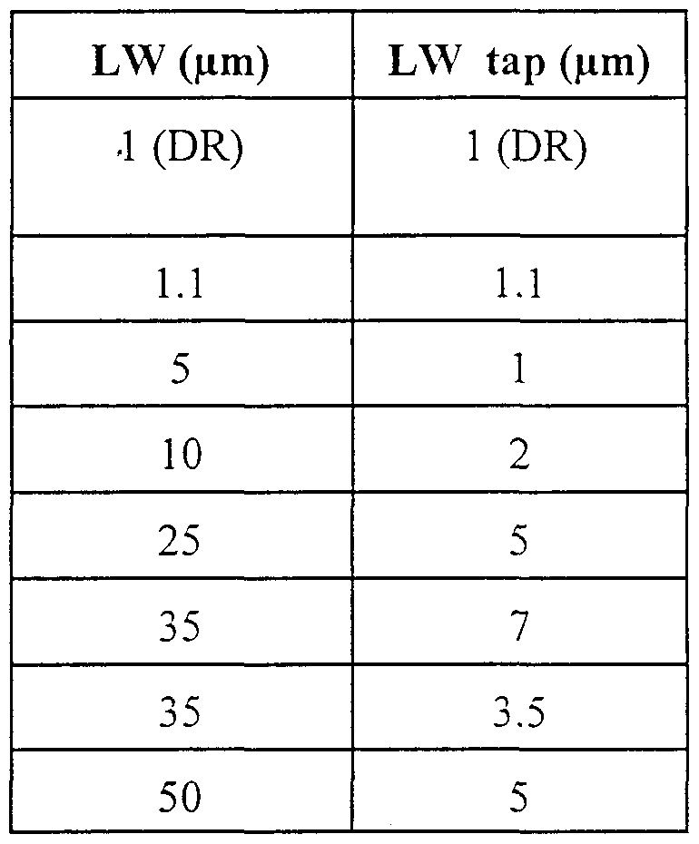
- the line width (LW) and the LW tap are the parameters that are varied. Table I shows the variations in the van der Pauw structures in the exemplary metal short flow chip described herein.
- the nest defect size distribution structures are arrays of nested continuous lines designed for opens and shorts detection and for the extraction of defect size distribution.
- Line width and space between the line are the parameters that are varied to facilitate the extraction of defect size distribution.
- these structures occupy 50% of the chip area at locations 92 and 94 shown in Figure 9 and have fourteen variants in a total of ten cells 96.
- the amount of area these structures can occupy needs to be large enough to accurately detect less than 0.25 defects/cm 2 for one wafer.
- the number of variants typically include the design rule (DR), slightly below DR, slightly above DR and substantially above DR. Therefore, for example, if DR is 1.0 ⁇ m for line spacing, the plots might be for 0.9, 1.1 , 1.3 and 2.5 as shown in Table II. TABLE II
- Each cell is split into six sub-cells to reduce the line resistance to reasonable levels (less than 250 k ⁇ ) and to minimize the incidence of multiple defects per cell.
- An exemplary nest defect size distribution structure itself, generaly designated 1002, is depicted in Figure 10.
- the nest defect size distribution structures are designed such that the line width (LW) is equal to the spacing (S) between the lines to simplify subsequent analysis of data.
- the Kelvin metal critical dimension (CD) structures are made up of a continuous straight line with terminal connections at each end. These structures allow for precise line resistance measurements which, in conjunction with the sheet resistance determined from the van der Pauw structures, allow for the determination of Kelvin line width. These structures are designed primarily to determine the variation in the electrical critical dimension.
- An exemplar ⁇ ' Kelvin critical dimension structure, generally designated 110, is depicted in Figure 11.
- the parameters varied for the local neighborhood are the number 112, line width 114 and space 116 of the lines.
- the global environment 118 around the Kelvin structures is also varied, primarily to study etch related effects on the electrical critical dimension (see Figure 11). Parameters varied for global neighborhood are the density and area.
- the global neighborhood structures can also serve other electrical measurement needs. For example, the yield of these structures can be measured so that not only metal critical dimension as a function of environment is obtained, but also yield as a function of environment.
- Figure 12 depicts the location of Kelvin structures 122 in the metal short flow chip described herein. These locations are chosen to cover available area. Tables III through IX describe the variations in the Kelvin structures used in the metal short flow chip described herein. These values were chosen as to cover the space identified in Figure 22(a) through 22(b). For example, the pattern density is centered around 45% and the line width and spaces are in the range of 1.0 to 3.3 ⁇ m since this is where most of an exemplary product layout is centered.
- the snake, comb and snake & comb structures are designed primarily for the detection of shorts and opens across a wide variety of patterns.
- Snakes are used primarily for the detection of opens and can also be used for monitoring resistance variation.
- Combs are used for monitoring shorts.
- Shorts and opens are fundamental yield loss mechanisms and both need to be minimized to obtain high product yield.
- Figure 13 shows the location of snakes and combs 1302 in the metal short flow chip described herein.
- Quadrant one 1304 also contains snakes 1402 and combs 1404 nested within the Kelvin structures asshown, for example in Figure 14.
- Line width (LW) and space (S), see Figure 14 are the parameters varied on these structures to study their impact on shorts and opens.
- Tables X through XIII describe the variations of snake and comb structures used in the metal short flow chip described herein. Again, the parameters were chosen such that the space covered in line width, line space, and density is similar to that seen in the example product layout, as shown in Figure 22(a) through 22(c).
- Border and fringe structures are designed to study the impact of optical proximity correction (OPC) structures on shorts. These optical proximity corrections are usually added to improve via yields. However, it is necessary to check metal short yield with and without these borders to ensure that there is no detrimental impact to short yield. Borders 1502 are placed both at the end of the comb lines and in the interior of comb structures, generally designated 1504, as shown in Figure 15. Figure 16 shows the location of border structures, generally designated 1602, in the metal short flow chip described herein.
- OPC optical proximity correction
- SEM Scanning electron microscopy
- the extraction engine 18 has two main purposes: (1) it is used in determining the range of levels (e.g. linewidth, linespace, density) to use when designing a characterization vehicle. (2) It is used to extract the attributes of a product layout which are then subsequently used in the yield models to predict yield. (1) has already been described above with reference to how the line width, space and density of the snake, comb and Kelvin structures were chosen in the example characterization vehicle. Thus, most of the following discussion focuses on (2).
- levels e.g. linewidth, linespace, density
- the characterization vehicle drives which attributes to extract. The process consists of:
- the yield model 16 is preferably constructed from data measured from at least a portion of a wafer which has undergone the selected fabrication process steps using the reticle set defined by the characterization vehicle 12.
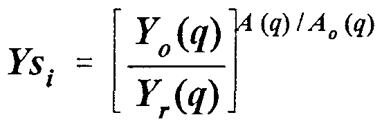
- the yield is modeled as a product of random and systematic components:
- AREA BASED MODELS The area based model can be written as:
- Y 0 (q) is the yield of a structure with design factor q from the characterization vehicle.
- a 0 (q) is the shortable area of this structure and A(q) is the shortable area of all instances of type q on the product layout.
- Y r (q) is the predicted yield of this structure assuming random defects were the only yield loss mechanism. The procedure for calculating this quantity is described below in connection with random yield modeling. The definition of shortable area is best illustrated with the example shown in Figure 18. This type of test structure can be used to determine if the fab is capable of yielding wide lines that have a bend with a spacing of s.
- a short is measured by applying a voltage between terminal (1) and (2) and measuring the current flowing from terminal (1) to (2). If this current is larger than a specified threshold (usually 1-lOOnA), a short is detected.
- the shortable area is defined to be the area where if a bridging occurs, a short will be measured. In the example of Figure 18, the shortable area is approximately x*s).
- the A(q) term is the shortable area of all occurrences of the exact or nearly exact patten (i.e. a large line with a spacing of s and a bend of 45 degrees) shown in Figure 18 in a product layout.
- the Yr(q) term is extracted by predicting the random yield limit of this particular structure using the critical area method described below.
- Ni(q) is the number of times the unit cell pattern or very similar unit cell pattern to the test pattern on the characterization vehicle appears on the product layout.
- No(q) is the number of times the unit cell pattern appears on the characterization vehicle.
- the random component can be written as:
- CA(x) is the critical area of defect size x
- DSD(x) is the defective size distribution, as also described in"Modeling of Lithography Related Yield Losses for CAD of VSLI Circuits", W. Maly, IEEE Trans, on CAD, July 1985, ppl61-177, which is incorporated by reference as if fully set forth herein.
- Xo is the smallest defect size which can be confidently observed or measured. This is usually set at the minimum line space design rule.
- the critical area is the area where if a defect of size x landed, a short would occur. For very small x, the critical area is near 0 while very large defect sizes have a critical area approaching the entire area of the chip. Additional description of critical area and extraction techniques can be found in P. K. Nag and W. Maly,
- the defect size distribution represents the defect density of defects of size x.
- There are many proposed models for defect size distributions see, for example, "Yield Models -
- P is a unitless value which represents the rate at which defects decay over size.
- p is between 2 and 4.
- K is a normalization factor such that
- the nest structure is designed for extracting defect size distributions. It is composed of N lines of width w and space s as shown in Figure 20. This structure is tested by measuring the shorting current between lines 1 and 2, 2 and 3, 3 and 4, ..., and N-1 and N. Any current above a given spec limit is deemed a short. In addition, opens can be testing by measuring the resistance of lines 1, 2, 3, ...., N-1, and N. Any resistance above a certain spec limit is deemed to be an open line. By examining how many lines are shorted together the defect size distribution can be determined.
- the defect size must be greater than s and no larger than 3w + 2s. Any defects smaller than s will not cause a short at all while defects larger than 3w+2s are guaranteed to cause a short of at least 3 lines. For each number of lines shorted, an interval of sizes can be created:
- targets are ascribed to each module listed in the spread sheet. The further a module yield is away from a target, the more emphasis and resources are devoted to fixing the problem.
Abstract
Description


Claims
Priority Applications (4)
| Application Number | Priority Date | Filing Date | Title |
|---|---|---|---|
| EP00980490A EP1384179A4 (en) | 1999-11-18 | 2000-11-17 | System and method for product yield prediction |
| JP2001537527A JP2004505433A (en) | 1999-11-18 | 2000-11-17 | System and method for product yield prediction |
| AU17744/01A AU1774401A (en) | 1999-11-18 | 2000-11-17 | System and method for product yield prediction |
| US10/200,045 US6901564B2 (en) | 1999-11-18 | 2002-07-18 | System and method for product yield prediction |
Applications Claiming Priority (2)
| Application Number | Priority Date | Filing Date | Title |
|---|---|---|---|
| US09/442,699 | 1999-11-18 | ||
| US09/442,699 US6449749B1 (en) | 1999-11-18 | 1999-11-18 | System and method for product yield prediction |
Publications (3)
| Publication Number | Publication Date |
|---|---|
| WO2001035718A2 true WO2001035718A2 (en) | 2001-05-25 |
| WO2001035718A9 WO2001035718A9 (en) | 2002-05-30 |
| WO2001035718A3 WO2001035718A3 (en) | 2003-10-30 |
Family
ID=23757795
Family Applications (2)
| Application Number | Title | Priority Date | Filing Date |
|---|---|---|---|
| PCT/US2000/031665 WO2001035718A2 (en) | 1999-11-18 | 2000-11-17 | System and method for product yield prediction |
| PCT/US2000/031528 WO2001037150A1 (en) | 1999-11-18 | 2000-11-17 | System and method for product yield prediction using device and process neighborhood characterization vehicle |
Family Applications After (1)
| Application Number | Title | Priority Date | Filing Date |
|---|---|---|---|
| PCT/US2000/031528 WO2001037150A1 (en) | 1999-11-18 | 2000-11-17 | System and method for product yield prediction using device and process neighborhood characterization vehicle |
Country Status (6)
| Country | Link |
|---|---|
| US (6) | US6449749B1 (en) |
| EP (1) | EP1384179A4 (en) |
| JP (2) | JP2004505433A (en) |
| CN (2) | CN1975741A (en) |
| AU (1) | AU1774401A (en) |
| WO (2) | WO2001035718A2 (en) |
Cited By (2)
| Publication number | Priority date | Publication date | Assignee | Title |
|---|---|---|---|---|
| US7197726B2 (en) | 2001-09-28 | 2007-03-27 | Pdf Solutions, Inc. | Test structures for estimating dishing and erosion effects in copper damascene technology |
| US7735053B2 (en) | 2006-06-29 | 2010-06-08 | Sharp Kabushiki Kaisha | Correction method and correction system for design data or mask data, validation method and validation system for design data or mask data, yield estimation method for semiconductor integrated circuit, method for improving design rule, mask production method, and semiconductor integrated circuit production method |
Families Citing this family (120)
| Publication number | Priority date | Publication date | Assignee | Title |
|---|---|---|---|---|
| US6449749B1 (en) * | 1999-11-18 | 2002-09-10 | Pdf Solutions, Inc. | System and method for product yield prediction |
| US6738954B1 (en) * | 1999-12-08 | 2004-05-18 | International Business Machines Corporation | Method for prediction random defect yields of integrated circuits with accuracy and computation time controls |
| US6560766B2 (en) * | 2001-07-26 | 2003-05-06 | Numerical Technologies, Inc. | Method and apparatus for analyzing a layout using an instance-based representation |
| WO2003028412A2 (en) * | 2001-08-31 | 2003-04-03 | Pdf Solutions, Inc. | Test structures and models for estimating the yield impact of dishing and/or voids |
| US6681376B1 (en) * | 2001-10-17 | 2004-01-20 | Cypress Semiconductor Corporation | Integrated scheme for semiconductor device verification |
| US6751519B1 (en) * | 2001-10-25 | 2004-06-15 | Kla-Tencor Technologies Corporation | Methods and systems for predicting IC chip yield |
| US6918101B1 (en) | 2001-10-25 | 2005-07-12 | Kla -Tencor Technologies Corporation | Apparatus and methods for determining critical area of semiconductor design data |
| US6948141B1 (en) | 2001-10-25 | 2005-09-20 | Kla-Tencor Technologies Corporation | Apparatus and methods for determining critical area of semiconductor design data |
| US6966047B1 (en) * | 2002-04-09 | 2005-11-15 | Kla-Tencor Technologies Corporation | Capturing designer intent in reticle inspection |
| US6826738B2 (en) * | 2002-05-10 | 2004-11-30 | Pdf Solutions, Inc. | Optimization of die placement on wafers |
| US6914443B2 (en) * | 2002-07-24 | 2005-07-05 | Applied Materials Israel, Ltd. | Apparatus and method for enhanced voltage contrast analysis |
| AU2003297025A1 (en) * | 2002-12-11 | 2004-06-30 | Pdf Solutions, Inc. | Fast localization of electrical failures on an integrated circuit system and method |
| US6898780B2 (en) * | 2002-12-20 | 2005-05-24 | Lsi Logic Corporation | Method and system for constructing a hierarchy-driven chip covering for optical proximity correction |
| EP1579352A2 (en) * | 2003-01-02 | 2005-09-28 | PDF Solutions, Inc. | Yield improvement |
| US7346470B2 (en) * | 2003-06-10 | 2008-03-18 | International Business Machines Corporation | System for identification of defects on circuits or other arrayed products |
| US7752581B2 (en) * | 2003-06-10 | 2010-07-06 | International Business Machines Corporation | Design structure and system for identification of defects on circuits or other arrayed products |
| US7558419B1 (en) | 2003-08-14 | 2009-07-07 | Brion Technologies, Inc. | System and method for detecting integrated circuit pattern defects |
| US7730434B2 (en) * | 2003-08-25 | 2010-06-01 | Tau-Metrix, Inc. | Contactless technique for evaluating a fabrication of a wafer |
| US7013441B2 (en) * | 2003-09-26 | 2006-03-14 | International Business Machines Corporation | Method for modeling integrated circuit yield |
| US7003758B2 (en) * | 2003-10-07 | 2006-02-21 | Brion Technologies, Inc. | System and method for lithography simulation |
| JP2007531983A (en) * | 2003-10-15 | 2007-11-08 | ピー・デイ・エフ ソリユーシヨンズ インコーポレイテツド | Method and arrangement for connecting test structures or line arrays for monitoring integrated circuit manufacturing |
| DE10355573B4 (en) * | 2003-11-28 | 2007-12-20 | Advanced Micro Devices, Inc., Sunnyvale | A method of increasing production yield by controlling lithography based on electrical velocity data |
| US7251793B1 (en) * | 2004-02-02 | 2007-07-31 | Advanced Micro Devices, Inc. | Predicting defect future effects in integrated circuit technology development to facilitate semiconductor wafer lot disposition |
| US7849366B1 (en) * | 2004-03-26 | 2010-12-07 | Advanced Micro Devices, Inc. | Method and apparatus for predicting yield parameters based on fault classification |
| US8818784B1 (en) * | 2004-06-23 | 2014-08-26 | Cypress Semiconductor Corporation | Hardware description language (HDL) incorporating statistically derived data and related methods |
| TW200622275A (en) * | 2004-09-06 | 2006-07-01 | Mentor Graphics Corp | Integrated circuit yield and quality analysis methods and systems |
| US7496478B2 (en) | 2005-07-18 | 2009-02-24 | Dieter Rathei | Method of monitoring a semiconductor manufacturing trend |
| US20070016321A1 (en) * | 2005-07-18 | 2007-01-18 | Dieter Rathei | Method for screening risk quality semiconductor products |
| US7318206B2 (en) * | 2005-09-30 | 2008-01-08 | International Business Machines Corporation | Offset determination for measurement system matching |
| US7187179B1 (en) | 2005-10-19 | 2007-03-06 | International Business Machines Corporation | Wiring test structures for determining open and short circuits in semiconductor devices |
| US7386815B2 (en) | 2005-10-27 | 2008-06-10 | International Business Machines Corporation | Test yield estimate for semiconductor products created from a library |
| US7469394B1 (en) * | 2005-12-09 | 2008-12-23 | Altera Corporation | Timing variation aware compilation |
| KR100703982B1 (en) * | 2006-01-23 | 2007-04-09 | 삼성전자주식회사 | Method for analyzing layout of semiconductor integrate circuit device, system for analyzing layout of semiconductor integrate circuit device, standard cell library, mask and semiconductor integrate circuit device |
| US7477961B2 (en) * | 2006-05-12 | 2009-01-13 | International Business Machines Corporation | Equivalent gate count yield estimation for integrated circuit devices |
| DE102006025351B4 (en) * | 2006-05-31 | 2013-04-04 | Globalfoundries Inc. | Test structure for monitoring leakage currents in a metallization layer and method |
| US7761824B2 (en) * | 2006-07-05 | 2010-07-20 | Chew Marko P | System and method to generate an IC layout using simplified manufacturing rule |
| KR101269055B1 (en) * | 2006-08-19 | 2013-05-29 | 삼성전자주식회사 | Method for increasing the yield of layout and the recording medium having the same |
| US7448008B2 (en) * | 2006-08-29 | 2008-11-04 | International Business Machines Corporation | Method, system, and program product for automated verification of gating logic using formal verification |
| US7448018B2 (en) * | 2006-09-12 | 2008-11-04 | International Business Machines Corporation | System and method for employing patterning process statistics for ground rules waivers and optimization |
| DE102006051489B4 (en) * | 2006-10-31 | 2011-12-22 | Advanced Micro Devices, Inc. | Test structure for OPC-induced short circuits between lines in a semiconductor device and measurement method |
| US7886238B1 (en) * | 2006-11-28 | 2011-02-08 | Cadence Design Systems, Inc. | Visual yield analysis of intergrated circuit layouts |
| US7962866B2 (en) | 2006-12-29 | 2011-06-14 | Cadence Design Systems, Inc. | Method, system, and computer program product for determining three-dimensional feature characteristics in electronic designs |
| US20080162103A1 (en) * | 2006-12-29 | 2008-07-03 | Cadence Design Systems, Inc. | Method, system, and computer program product for concurrent model aided electronic design automation |
| US7827519B2 (en) | 2006-12-29 | 2010-11-02 | Cadence Design Systems, Inc. | Method, system, and computer program product for preparing multiple layers of semiconductor substrates for electronic designs |
| US8302036B2 (en) * | 2007-01-05 | 2012-10-30 | Freescale Semiconductor, Inc. | Method and apparatus for designing an integrated circuit |
| US7494893B1 (en) | 2007-01-17 | 2009-02-24 | Pdf Solutions, Inc. | Identifying yield-relevant process parameters in integrated circuit device fabrication processes |
| US20080178127A1 (en) * | 2007-01-19 | 2008-07-24 | Thomas J Dewkett | Silicon Multiple Core or Redundant Unit Optimization Tool |
| US7574682B2 (en) * | 2007-02-28 | 2009-08-11 | Freescale Semiconductor, Inc. | Yield analysis and improvement using electrical sensitivity extraction |
| US7962864B2 (en) * | 2007-05-24 | 2011-06-14 | Applied Materials, Inc. | Stage yield prediction |
| US7937179B2 (en) * | 2007-05-24 | 2011-05-03 | Applied Materials, Inc. | Dynamic inline yield analysis and prediction of a defect limited yield using inline inspection defects |
| US8799831B2 (en) * | 2007-05-24 | 2014-08-05 | Applied Materials, Inc. | Inline defect analysis for sampling and SPC |
| US8924904B2 (en) * | 2007-05-24 | 2014-12-30 | Applied Materials, Inc. | Method and apparatus for determining factors for design consideration in yield analysis |
| US20080312875A1 (en) * | 2007-06-12 | 2008-12-18 | Yu Guanyuan M | Monitoring and control of integrated circuit device fabrication processes |
| US7902852B1 (en) | 2007-07-10 | 2011-03-08 | Pdf Solutions, Incorporated | High density test structure array to support addressable high accuracy 4-terminal measurements |
| US7974723B2 (en) * | 2008-03-06 | 2011-07-05 | Applied Materials, Inc. | Yield prediction feedback for controlling an equipment engineering system |
| US8001495B2 (en) * | 2008-04-17 | 2011-08-16 | International Business Machines Corporation | System and method of predicting problematic areas for lithography in a circuit design |
| US7682842B2 (en) * | 2008-05-30 | 2010-03-23 | International Business Machines Corporation | Method of adaptively selecting chips for reducing in-line testing in a semiconductor manufacturing line |
| DE102008062153A1 (en) | 2008-12-17 | 2010-12-30 | Grenzebach Maschinenbau Gmbh | Method and device for rapid transport of glass plates |
| US8082055B2 (en) * | 2009-07-08 | 2011-12-20 | Taiwan Semiconductor Manufacturing Company, Ltd. | Method for a bin ratio forecast at new tape out stage |
| US8421162B2 (en) | 2009-09-30 | 2013-04-16 | Suvolta, Inc. | Advanced transistors with punch through suppression |
| US8273617B2 (en) | 2009-09-30 | 2012-09-25 | Suvolta, Inc. | Electronic devices and systems, and methods for making and using the same |
| US8650518B2 (en) * | 2010-01-08 | 2014-02-11 | Cadence Design Systems, Inc. | Method and apparatus for rule-based automatic layout parasitic extraction in a multi-technology environment |
| US8219964B2 (en) * | 2010-01-14 | 2012-07-10 | International Business Machines Corporation | Method for creating electrically testable patterns |
| US8276102B2 (en) | 2010-03-05 | 2012-09-25 | International Business Machines Corporation | Spatial correlation-based estimation of yield of integrated circuits |
| US8530286B2 (en) | 2010-04-12 | 2013-09-10 | Suvolta, Inc. | Low power semiconductor transistor structure and method of fabrication thereof |
| US8569128B2 (en) | 2010-06-21 | 2013-10-29 | Suvolta, Inc. | Semiconductor structure and method of fabrication thereof with mixed metal types |
| US8759872B2 (en) | 2010-06-22 | 2014-06-24 | Suvolta, Inc. | Transistor with threshold voltage set notch and method of fabrication thereof |
| US8594963B2 (en) * | 2010-09-01 | 2013-11-26 | Macronix International Co., Ltd. | In-line inspection yield prediction system |
| JP5566265B2 (en) * | 2010-11-09 | 2014-08-06 | 東京エレクトロン株式会社 | Substrate processing apparatus, program, computer storage medium, and substrate transfer method |
| US8404551B2 (en) | 2010-12-03 | 2013-03-26 | Suvolta, Inc. | Source/drain extension control for advanced transistors |
| US8461875B1 (en) | 2011-02-18 | 2013-06-11 | Suvolta, Inc. | Digital circuits having improved transistors, and methods therefor |
| US8525271B2 (en) | 2011-03-03 | 2013-09-03 | Suvolta, Inc. | Semiconductor structure with improved channel stack and method for fabrication thereof |
| US8400219B2 (en) | 2011-03-24 | 2013-03-19 | Suvolta, Inc. | Analog circuits having improved transistors, and methods therefor |
| US8748270B1 (en) | 2011-03-30 | 2014-06-10 | Suvolta, Inc. | Process for manufacturing an improved analog transistor |
| US8796048B1 (en) | 2011-05-11 | 2014-08-05 | Suvolta, Inc. | Monitoring and measurement of thin film layers |
| US8999861B1 (en) | 2011-05-11 | 2015-04-07 | Suvolta, Inc. | Semiconductor structure with substitutional boron and method for fabrication thereof |
| US8811068B1 (en) | 2011-05-13 | 2014-08-19 | Suvolta, Inc. | Integrated circuit devices and methods |
| US8569156B1 (en) | 2011-05-16 | 2013-10-29 | Suvolta, Inc. | Reducing or eliminating pre-amorphization in transistor manufacture |
| US8735987B1 (en) | 2011-06-06 | 2014-05-27 | Suvolta, Inc. | CMOS gate stack structures and processes |
| US8995204B2 (en) | 2011-06-23 | 2015-03-31 | Suvolta, Inc. | Circuit devices and methods having adjustable transistor body bias |
| US8629016B1 (en) | 2011-07-26 | 2014-01-14 | Suvolta, Inc. | Multiple transistor types formed in a common epitaxial layer by differential out-diffusion from a doped underlayer |
| WO2013022753A2 (en) | 2011-08-05 | 2013-02-14 | Suvolta, Inc. | Semiconductor devices having fin structures and fabrication methods thereof |
| US8748986B1 (en) | 2011-08-05 | 2014-06-10 | Suvolta, Inc. | Electronic device with controlled threshold voltage |
| US8645878B1 (en) | 2011-08-23 | 2014-02-04 | Suvolta, Inc. | Porting a circuit design from a first semiconductor process to a second semiconductor process |
| US8614128B1 (en) | 2011-08-23 | 2013-12-24 | Suvolta, Inc. | CMOS structures and processes based on selective thinning |
| US9129076B2 (en) | 2011-09-05 | 2015-09-08 | United Microelectronics Corp. | Hierarchical wafer yield prediction method and hierarchical lifetime prediction method |
| US8713511B1 (en) | 2011-09-16 | 2014-04-29 | Suvolta, Inc. | Tools and methods for yield-aware semiconductor manufacturing process target generation |
| US9236466B1 (en) | 2011-10-07 | 2016-01-12 | Mie Fujitsu Semiconductor Limited | Analog circuits having improved insulated gate transistors, and methods therefor |
| US8832621B1 (en) | 2011-11-28 | 2014-09-09 | Cadence Design Systems, Inc. | Topology design using squish patterns |
| US8895327B1 (en) | 2011-12-09 | 2014-11-25 | Suvolta, Inc. | Tipless transistors, short-tip transistors, and methods and circuits therefor |
| US8819603B1 (en) | 2011-12-15 | 2014-08-26 | Suvolta, Inc. | Memory circuits and methods of making and designing the same |
| US8883600B1 (en) | 2011-12-22 | 2014-11-11 | Suvolta, Inc. | Transistor having reduced junction leakage and methods of forming thereof |
| US8599623B1 (en) | 2011-12-23 | 2013-12-03 | Suvolta, Inc. | Circuits and methods for measuring circuit elements in an integrated circuit device |
| US8970289B1 (en) | 2012-01-23 | 2015-03-03 | Suvolta, Inc. | Circuits and devices for generating bi-directional body bias voltages, and methods therefor |
| US8877619B1 (en) | 2012-01-23 | 2014-11-04 | Suvolta, Inc. | Process for manufacture of integrated circuits with different channel doping transistor architectures and devices therefrom |
| US9093550B1 (en) | 2012-01-31 | 2015-07-28 | Mie Fujitsu Semiconductor Limited | Integrated circuits having a plurality of high-K metal gate FETs with various combinations of channel foundation structure and gate stack structure and methods of making same |
| US9406567B1 (en) | 2012-02-28 | 2016-08-02 | Mie Fujitsu Semiconductor Limited | Method for fabricating multiple transistor devices on a substrate with varying threshold voltages |
| US8863064B1 (en) | 2012-03-23 | 2014-10-14 | Suvolta, Inc. | SRAM cell layout structure and devices therefrom |
| US8631375B2 (en) | 2012-04-10 | 2014-01-14 | International Business Machines Corporation | Via selection in integrated circuit design |
| US9299698B2 (en) | 2012-06-27 | 2016-03-29 | Mie Fujitsu Semiconductor Limited | Semiconductor structure with multiple transistors having various threshold voltages |
| US9058034B2 (en) * | 2012-08-09 | 2015-06-16 | International Business Machines Corporation | Integrated circuit product yield optimization using the results of performance path testing |
| US8539429B1 (en) * | 2012-08-13 | 2013-09-17 | International Business Machines Corporation | System yield optimization using the results of integrated circuit chip performance path testing |
| US8745553B2 (en) * | 2012-08-23 | 2014-06-03 | Globalfoundries Inc. | Method and apparatus for applying post graphic data system stream enhancements |
| US8637955B1 (en) | 2012-08-31 | 2014-01-28 | Suvolta, Inc. | Semiconductor structure with reduced junction leakage and method of fabrication thereof |
| US9112057B1 (en) | 2012-09-18 | 2015-08-18 | Mie Fujitsu Semiconductor Limited | Semiconductor devices with dopant migration suppression and method of fabrication thereof |
| US9041126B2 (en) | 2012-09-21 | 2015-05-26 | Mie Fujitsu Semiconductor Limited | Deeply depleted MOS transistors having a screening layer and methods thereof |
| US9524916B2 (en) | 2012-10-31 | 2016-12-20 | International Business Machines Corporation | Structures and methods for determining TDDB reliability at reduced spacings using the structures |
| CN104854698A (en) | 2012-10-31 | 2015-08-19 | 三重富士通半导体有限责任公司 | Dram-type device with low variation transistor peripheral circuits, and related methods |
| US8816754B1 (en) | 2012-11-02 | 2014-08-26 | Suvolta, Inc. | Body bias circuits and methods |
| US9093997B1 (en) | 2012-11-15 | 2015-07-28 | Mie Fujitsu Semiconductor Limited | Slew based process and bias monitors and related methods |
| US9070477B1 (en) | 2012-12-12 | 2015-06-30 | Mie Fujitsu Semiconductor Limited | Bit interleaved low voltage static random access memory (SRAM) and related methods |
| US9112484B1 (en) | 2012-12-20 | 2015-08-18 | Mie Fujitsu Semiconductor Limited | Integrated circuit process and bias monitors and related methods |
| US9922161B2 (en) * | 2013-02-27 | 2018-03-20 | The Regents Of The University Of California | IC layout adjustment method and tool for improving dielectric reliability at interconnects |
| US9268885B1 (en) | 2013-02-28 | 2016-02-23 | Mie Fujitsu Semiconductor Limited | Integrated circuit device methods and models with predicted device metric variations |
| US9299801B1 (en) | 2013-03-14 | 2016-03-29 | Mie Fujitsu Semiconductor Limited | Method for fabricating a transistor device with a tuned dopant profile |
| US9478571B1 (en) | 2013-05-24 | 2016-10-25 | Mie Fujitsu Semiconductor Limited | Buried channel deeply depleted channel transistor |
| US9710006B2 (en) | 2014-07-25 | 2017-07-18 | Mie Fujitsu Semiconductor Limited | Power up body bias circuits and methods |
| US9319013B2 (en) | 2014-08-19 | 2016-04-19 | Mie Fujitsu Semiconductor Limited | Operational amplifier input offset correction with transistor threshold voltage adjustment |
| CN112784519A (en) * | 2019-11-05 | 2021-05-11 | 鸿富锦精密电子(天津)有限公司 | PCB routing parameter setting device and method and storage medium |
| US11456224B2 (en) * | 2020-08-11 | 2022-09-27 | Nanya Technology Corporation | Semiconductor structure with test structure |
Family Cites Families (53)
| Publication number | Priority date | Publication date | Assignee | Title |
|---|---|---|---|---|
| US3751647A (en) * | 1971-09-22 | 1973-08-07 | Ibm | Semiconductor and integrated circuit device yield modeling |
| JPS5453864A (en) * | 1977-10-05 | 1979-04-27 | Sanyo Electric Co Ltd | Monitoring method of line widths |
| US4835486A (en) * | 1986-04-28 | 1989-05-30 | Burr-Brown Corporation | Isolation amplifier with precise timing of signals coupled across isolation barrier |
| US4795964A (en) | 1986-08-01 | 1989-01-03 | Texas Instruments Incorporated | Method and apparatus for measuring the capacitance of complementary field-effect transistor devices |
| US4835466A (en) * | 1987-02-06 | 1989-05-30 | Fairchild Semiconductor Corporation | Apparatus and method for detecting spot defects in integrated circuits |
| JP2695160B2 (en) | 1987-04-30 | 1997-12-24 | 株式会社日立製作所 | Calculation method of resistance between terminals of arbitrarily shaped resistor |
| US5070469A (en) | 1988-11-29 | 1991-12-03 | Mitsubishi Denki Kabushiki Kaisha | Topography simulation method |
| US5067101A (en) | 1988-11-29 | 1991-11-19 | Mitsubishi Denki Kabushiki Kaisha | Topography simulation method |
| US5068547A (en) | 1990-09-05 | 1991-11-26 | Lsi Logic Corporation | Process monitor circuit |
| JPH04167537A (en) * | 1990-10-31 | 1992-06-15 | Matsushita Electric Ind Co Ltd | Test chip |
| JP2679500B2 (en) | 1990-12-17 | 1997-11-19 | モトローラ・インコーポレイテッド | Method for calculating overall system yield |
| US5301118A (en) | 1991-11-18 | 1994-04-05 | International Business Machines Corporation | Monte carlo simulation design methodology |
| US5798649A (en) | 1991-12-26 | 1998-08-25 | Texas Instruments Incorporated | Method for detecting defects in semiconductor insulators |
| JP2729130B2 (en) | 1992-04-16 | 1998-03-18 | 三菱電機株式会社 | Semiconductor device manufacturing parameter setting method and apparatus |
| JP2914040B2 (en) * | 1992-09-22 | 1999-06-28 | 日産自動車株式会社 | Driving force distribution control device for four-wheel drive vehicle |
| US5286656A (en) | 1992-11-02 | 1994-02-15 | National Semiconductor Corporation | Individualized prepackage AC performance testing of IC dies on a wafer using DC parametric test patterns |
| JP3352153B2 (en) * | 1993-06-17 | 2002-12-03 | 株式会社東芝 | Water distribution flow prediction device |
| JP3001351B2 (en) | 1993-06-24 | 2000-01-24 | 日本電気株式会社 | Simulation method |
| JPH0746895A (en) | 1993-07-29 | 1995-02-14 | Canon Inc | Stepping motor drive circuit |
| JP3039210B2 (en) | 1993-08-03 | 2000-05-08 | 日本電気株式会社 | Method for manufacturing semiconductor device |
| US5497381A (en) * | 1993-10-15 | 1996-03-05 | Analog Devices, Inc. | Bitstream defect analysis method for integrated circuits |
| IL109268A (en) | 1994-04-10 | 1999-01-26 | Advanced Recognition Tech | Pattern recognition method and system |
| JPH0851159A (en) * | 1994-08-05 | 1996-02-20 | Mitsubishi Electric Corp | Semiconductor integrated circuit |
| US5486786A (en) | 1994-08-09 | 1996-01-23 | Lsi Logic Corporation | Process monitor for CMOS integrated circuits |
| JPH08148537A (en) | 1994-11-18 | 1996-06-07 | Toshiba Corp | Semiconductor integrated circuit |
| JP3986571B2 (en) * | 1994-12-09 | 2007-10-03 | 日本テキサス・インスツルメンツ株式会社 | Yield prediction apparatus and method |
| US5646870A (en) | 1995-02-13 | 1997-07-08 | Advanced Micro Devices, Inc. | Method for setting and adjusting process parameters to maintain acceptable critical dimensions across each die of mass-produced semiconductor wafers |
| US5598341A (en) * | 1995-03-10 | 1997-01-28 | Advanced Micro Devices, Inc. | Real-time in-line defect disposition and yield forecasting system |
| US6072804A (en) | 1995-05-24 | 2000-06-06 | Thomson Consumer Electronics, Inc. | Ring bus data transfer system |
| JP2770788B2 (en) | 1995-06-13 | 1998-07-02 | 富士ゼロックス株式会社 | Ring bus multiprocessor device and processor board for configuring ring bus multiprocessor device |
| JPH098085A (en) * | 1995-06-16 | 1997-01-10 | Casio Comput Co Ltd | Yield forecast method for board |
| JPH09306837A (en) * | 1996-05-14 | 1997-11-28 | Kanegafuchi Chem Ind Co Ltd | Thin film semiconductor and its manufacture |
| US5867033A (en) | 1996-05-24 | 1999-02-02 | Lsi Logic Corporation | Circuit for testing the operation of a semiconductor device |
| US5767542A (en) | 1996-05-28 | 1998-06-16 | Analog Devices, Inc. | Matching parasitic capacitances and characteristics of field effect transistors |
| US5852581A (en) | 1996-06-13 | 1998-12-22 | Micron Technology, Inc. | Method of stress testing memory integrated circuits |
| US5790479A (en) | 1996-09-17 | 1998-08-04 | Xilinx, Inc. | Method for characterizing interconnect timing characteristics using reference ring oscillator circuit |
| US6075418A (en) | 1996-09-17 | 2000-06-13 | Xilinx, Inc. | System with downstream set or clear for measuring signal propagation delays on integrated circuits |
| US5773315A (en) * | 1996-10-28 | 1998-06-30 | Advanced Micro Devices, Inc. | Product wafer yield prediction method employing a unit cell approach |
| US5966527A (en) | 1996-10-28 | 1999-10-12 | Advanced Micro Devices, Inc. | Apparatus, article of manufacture, method and system for simulating a mass-produced semiconductor device behavior |
| US5822258A (en) | 1997-05-05 | 1998-10-13 | Micron Technology, Inc. | Circuit and method for testing a memory device with a cell plate generator having a variable current |
| US6066179A (en) | 1997-06-13 | 2000-05-23 | University Of Edinburgh | Property estimation of an integrated circuit |
| US5903012A (en) | 1997-07-28 | 1999-05-11 | International Business Machines Corporation | Process variation monitor for integrated circuits |
| US6118137A (en) | 1997-09-08 | 2000-09-12 | Advanced Micro Devices, Inc. | Test structure responsive to electrical signals for determining lithographic misalignment of conductors relative to vias |
| JP3895851B2 (en) * | 1997-12-09 | 2007-03-22 | 株式会社東芝 | Mask pattern correction method |
| US6075417A (en) | 1998-01-05 | 2000-06-13 | Advanced Micro Devices, Inc. | Ring oscillator test structure |
| US6124143A (en) | 1998-01-26 | 2000-09-26 | Lsi Logic Corporation | Process monitor circuitry for integrated circuits |
| JP3739201B2 (en) * | 1998-03-06 | 2006-01-25 | 富士通株式会社 | Semiconductor chip correlation analysis method and apparatus, semiconductor chip yield adjustment method, and storage medium |
| US6063132A (en) | 1998-06-26 | 2000-05-16 | International Business Machines Corporation | Method for verifying design rule checking software |
| US6393602B1 (en) * | 1998-10-21 | 2002-05-21 | Texas Instruments Incorporated | Method of a comprehensive sequential analysis of the yield losses of semiconductor wafers |
| US6134191A (en) | 1999-02-26 | 2000-10-17 | Xilinx, Inc. | Oscillator for measuring on-chip delays |
| US6298470B1 (en) * | 1999-04-15 | 2001-10-02 | Micron Technology, Inc. | Method for efficient manufacturing of integrated circuits |
| US6184048B1 (en) | 1999-11-03 | 2001-02-06 | Texas Instruments Incorporated | Testing method and apparatus assuring semiconductor device quality and reliability |
| US6449749B1 (en) | 1999-11-18 | 2002-09-10 | Pdf Solutions, Inc. | System and method for product yield prediction |
-
1999
- 1999-11-18 US US09/442,699 patent/US6449749B1/en not_active Expired - Lifetime
-
2000
- 2000-11-17 WO PCT/US2000/031665 patent/WO2001035718A2/en active Application Filing
- 2000-11-17 CN CNA2006100941316A patent/CN1975741A/en active Pending
- 2000-11-17 JP JP2001537527A patent/JP2004505433A/en active Pending
- 2000-11-17 CN CNB008173575A patent/CN100336063C/en not_active Expired - Fee Related
- 2000-11-17 WO PCT/US2000/031528 patent/WO2001037150A1/en active Application Filing
- 2000-11-17 EP EP00980490A patent/EP1384179A4/en not_active Withdrawn
- 2000-11-17 AU AU17744/01A patent/AU1774401A/en not_active Abandoned
-
2002
- 2002-07-18 US US10/200,045 patent/US6901564B2/en not_active Expired - Fee Related
-
2005
- 2005-03-10 US US11/078,630 patent/US7174521B2/en not_active Expired - Fee Related
-
2006
- 2006-08-10 US US11/503,433 patent/US7373625B2/en not_active Expired - Lifetime
- 2006-08-10 US US11/503,323 patent/US7356800B2/en not_active Expired - Lifetime
-
2007
- 2007-03-30 JP JP2007095740A patent/JP2007201497A/en active Pending
-
2008
- 2008-05-13 US US12/119,862 patent/US7673262B2/en not_active Expired - Fee Related
Non-Patent Citations (4)
| Title |
|---|
| KHARE J.B.: 'Extraction of defect characteristics for yield estimation using the double bridge test structure' VLSITSA 1991, pages 428 - 432, XP010045317 * |
| KHARE J.B.: 'Yield-oriented computer-aided defect diagnosis' IEEE TRANSACTIONS ON SEMICONDUCTOR MANUFACTURING vol. 8, no. 2, May 1995, pages 195 - 206, XP002939180 * |
| NURANI ET AL.: 'In-line yield prediction methodologies using patterned wafer inspection information' IEEE TRANSACTIONS ON SEMICONDUCTOR MANUFACTURING vol. 11, no. 1, February 1998, pages 40 - 47, XP002953733 * |
| See also references of EP1384179A2 * |
Cited By (2)
| Publication number | Priority date | Publication date | Assignee | Title |
|---|---|---|---|---|
| US7197726B2 (en) | 2001-09-28 | 2007-03-27 | Pdf Solutions, Inc. | Test structures for estimating dishing and erosion effects in copper damascene technology |
| US7735053B2 (en) | 2006-06-29 | 2010-06-08 | Sharp Kabushiki Kaisha | Correction method and correction system for design data or mask data, validation method and validation system for design data or mask data, yield estimation method for semiconductor integrated circuit, method for improving design rule, mask production method, and semiconductor integrated circuit production method |
Also Published As
| Publication number | Publication date |
|---|---|
| JP2004505433A (en) | 2004-02-19 |
| US20030145292A1 (en) | 2003-07-31 |
| AU1774401A (en) | 2001-05-30 |
| US7373625B2 (en) | 2008-05-13 |
| US7356800B2 (en) | 2008-04-08 |
| EP1384179A4 (en) | 2006-06-07 |
| CN1975741A (en) | 2007-06-06 |
| CN100336063C (en) | 2007-09-05 |
| US7673262B2 (en) | 2010-03-02 |
| WO2001035718A3 (en) | 2003-10-30 |
| US20080282210A1 (en) | 2008-11-13 |
| US20060277506A1 (en) | 2006-12-07 |
| US20050158888A1 (en) | 2005-07-21 |
| US7174521B2 (en) | 2007-02-06 |
| US6449749B1 (en) | 2002-09-10 |
| EP1384179A2 (en) | 2004-01-28 |
| WO2001035718A9 (en) | 2002-05-30 |
| US20070118242A1 (en) | 2007-05-24 |
| CN1535436A (en) | 2004-10-06 |
| WO2001037150A1 (en) | 2001-05-25 |
| JP2007201497A (en) | 2007-08-09 |
| US6901564B2 (en) | 2005-05-31 |
Similar Documents
| Publication | Publication Date | Title |
|---|---|---|
| US6449749B1 (en) | System and method for product yield prediction | |
| Shen et al. | Inductive fault analysis of MOS integrated circuits | |
| US6795952B1 (en) | System and method for product yield prediction using device and process neighborhood characterization vehicle | |
| Kuo et al. | An overview of manufacturing yield and reliability modeling for semiconductor products | |
| Khare et al. | From contamination to defects, faults and yield loss: simulation and applications | |
| US8289508B2 (en) | Defect detection recipe definition | |
| WO2008086282A2 (en) | Methods and systems for using electrical information for a device being fabricated on a wafer to perform one or more defect-related functions | |
| WO2009129105A2 (en) | Methods and systems for determining a defect criticality index for defects on wafers | |
| Blanton et al. | Yield learning through physically aware diagnosis of IC-failure populations | |
| Stapper et al. | Evolution and accomplishments of VLSI yield management at IBM | |
| US20070114396A1 (en) | Critical area calculation method and yield calculation method | |
| Maly et al. | Deformations of IC structure in test and yield learning | |
| Mak et al. | Cache RAM inductive fault analysis with fab defect modeling | |
| Ciplickas et al. | Predictive yield modeling of VLSIC's | |
| Khare et al. | SRAM-based extraction of defect characteristics | |
| Nag et al. | Simulation of yield/cost learning curves with Y4 | |
| Schvan et al. | Yield projection based on electrical fault distribution and critical structure analysis | |
| Glang | Measurement and distribution of faults on defect test site chips | |
| Nahar | The yield models and defect density monitors for integrated circuit diagnosis | |
| Khare | Contamination-defect-fault relationship: Modeling and simulation | |
| CHIPS | 5 DEFECT MONITORING AND YIELD PROJECTION | |
| Appello et al. | Rapid root cause analysis and process change validation with design-centric volume diagnostics in production yield enhancement | |
| Gaston et al. | Yield prediction using calibrated critical area modelling | |
| Maynard et al. | Wafer line productivity optimization in a multi-technology multi-part-number fabricator | |
| Griep et al. | Design based failure analysis and yield improvement in CMOS‐circuits |
Legal Events
| Date | Code | Title | Description |
|---|---|---|---|
| AK | Designated states |
Kind code of ref document: A2 Designated state(s): AE AG AL AM AT AU AZ BA BB BG BR BY BZ CA CH CN CR CU CZ DE DK DM DZ EE ES FI GB GD GE GH GM HR HU ID IL IN IS JP KE KG KP KR KZ LC LK LR LS LT LU LV MA MD MG MK MN MW MX MZ NO NZ PL PT RO RU SD SE SG SI SK SL TJ TM TR TT TZ UA UG UZ VN YU ZA ZW |
|
| AL | Designated countries for regional patents |
Kind code of ref document: A2 Designated state(s): GH GM KE LS MW MZ SD SL SZ TZ UG ZW AM AZ BY KG KZ MD RU TJ TM AT BE CH CY DE DK ES FI FR GB GR IE IT LU MC NL PT SE TR BF BJ CF CG CI CM GA GN GW ML MR NE SN TD TG |
|
| 121 | Ep: the epo has been informed by wipo that ep was designated in this application | ||
| DFPE | Request for preliminary examination filed prior to expiration of 19th month from priority date (pct application filed before 20040101) | ||
| ENP | Entry into the national phase |
Ref country code: JP Ref document number: 2001 537527 Kind code of ref document: A Format of ref document f/p: F |
|
| AK | Designated states |
Kind code of ref document: C2 Designated state(s): AE AG AL AM AT AU AZ BA BB BG BR BY BZ CA CH CN CR CU CZ DE DK DM DZ EE ES FI GB GD GE GH GM HR HU ID IL IN IS JP KE KG KP KR KZ LC LK LR LS LT LU LV MA MD MG MK MN MW MX MZ NO NZ PL PT RO RU SD SE SG SI SK SL TJ TM TR TT TZ UA UG UZ VN YU ZA ZW |
|
| AL | Designated countries for regional patents |
Kind code of ref document: C2 Designated state(s): GH GM KE LS MW MZ SD SL SZ TZ UG ZW AM AZ BY KG KZ MD RU TJ TM AT BE CH CY DE DK ES FI FR GB GR IE IT LU MC NL PT SE TR BF BJ CF CG CI CM GA GN GW ML MR NE SN TD TG |
|
| COP | Corrected version of pamphlet |
Free format text: PAGES 1/15-15/15, DRAWINGS, REPLACED BY NEW PAGES 1/14-14/14; DUE TO LATE TRANSMITTAL BY THE RECEIVING OFFICE |
|
| WWE | Wipo information: entry into national phase |
Ref document number: 2000980490 Country of ref document: EP |
|
| WWE | Wipo information: entry into national phase |
Ref document number: 008173575 Country of ref document: CN |
|
| REG | Reference to national code |
Ref country code: DE Ref legal event code: 8642 |
|
| WWP | Wipo information: published in national office |
Ref document number: 2000980490 Country of ref document: EP |