WO2003104343A2 - Method for chemical mechanical polishing (cmp) of low-k dielectric materials - Google Patents
Method for chemical mechanical polishing (cmp) of low-k dielectric materials Download PDFInfo
- Publication number
- WO2003104343A2 WO2003104343A2 PCT/IB2003/002266 IB0302266W WO03104343A2 WO 2003104343 A2 WO2003104343 A2 WO 2003104343A2 IB 0302266 W IB0302266 W IB 0302266W WO 03104343 A2 WO03104343 A2 WO 03104343A2
- Authority
- WO
- WIPO (PCT)
- Prior art keywords
- polyoxyethylene
- nonionic surfactant
- alkyl
- amphiphilic nonionic
- polishing
- Prior art date
Links
Classifications
-
- C—CHEMISTRY; METALLURGY
- C09—DYES; PAINTS; POLISHES; NATURAL RESINS; ADHESIVES; COMPOSITIONS NOT OTHERWISE PROVIDED FOR; APPLICATIONS OF MATERIALS NOT OTHERWISE PROVIDED FOR
- C09G—POLISHING COMPOSITIONS; SKI WAXES
- C09G1/00—Polishing compositions
- C09G1/02—Polishing compositions containing abrasives or grinding agents
-
- B—PERFORMING OPERATIONS; TRANSPORTING
- B24—GRINDING; POLISHING
- B24D—TOOLS FOR GRINDING, BUFFING OR SHARPENING
- B24D3/00—Physical features of abrasive bodies, or sheets, e.g. abrasive surfaces of special nature; Abrasive bodies or sheets characterised by their constituents
-
- C—CHEMISTRY; METALLURGY
- C09—DYES; PAINTS; POLISHES; NATURAL RESINS; ADHESIVES; COMPOSITIONS NOT OTHERWISE PROVIDED FOR; APPLICATIONS OF MATERIALS NOT OTHERWISE PROVIDED FOR
- C09K—MATERIALS FOR MISCELLANEOUS APPLICATIONS, NOT PROVIDED FOR ELSEWHERE
- C09K3/00—Materials not provided for elsewhere
- C09K3/14—Anti-slip materials; Abrasives
- C09K3/1454—Abrasive powders, suspensions and pastes for polishing
- C09K3/1463—Aqueous liquid suspensions
-
- C—CHEMISTRY; METALLURGY
- C11—ANIMAL OR VEGETABLE OILS, FATS, FATTY SUBSTANCES OR WAXES; FATTY ACIDS THEREFROM; DETERGENTS; CANDLES
- C11D—DETERGENT COMPOSITIONS; USE OF SINGLE SUBSTANCES AS DETERGENTS; SOAP OR SOAP-MAKING; RESIN SOAPS; RECOVERY OF GLYCEROL
- C11D1/00—Detergent compositions based essentially on surface-active compounds; Use of these compounds as a detergent
- C11D1/66—Non-ionic compounds
-
- H—ELECTRICITY
- H01—ELECTRIC ELEMENTS
- H01L—SEMICONDUCTOR DEVICES NOT COVERED BY CLASS H10
- H01L21/00—Processes or apparatus adapted for the manufacture or treatment of semiconductor or solid state devices or of parts thereof
- H01L21/02—Manufacture or treatment of semiconductor devices or of parts thereof
- H01L21/04—Manufacture or treatment of semiconductor devices or of parts thereof the devices having at least one potential-jump barrier or surface barrier, e.g. PN junction, depletion layer or carrier concentration layer
- H01L21/18—Manufacture or treatment of semiconductor devices or of parts thereof the devices having at least one potential-jump barrier or surface barrier, e.g. PN junction, depletion layer or carrier concentration layer the devices having semiconductor bodies comprising elements of Group IV of the Periodic System or AIIIBV compounds with or without impurities, e.g. doping materials
- H01L21/30—Treatment of semiconductor bodies using processes or apparatus not provided for in groups H01L21/20 - H01L21/26
- H01L21/302—Treatment of semiconductor bodies using processes or apparatus not provided for in groups H01L21/20 - H01L21/26 to change their surface-physical characteristics or shape, e.g. etching, polishing, cutting
- H01L21/304—Mechanical treatment, e.g. grinding, polishing, cutting
-
- H—ELECTRICITY
- H01—ELECTRIC ELEMENTS
- H01L—SEMICONDUCTOR DEVICES NOT COVERED BY CLASS H10
- H01L21/00—Processes or apparatus adapted for the manufacture or treatment of semiconductor or solid state devices or of parts thereof
- H01L21/02—Manufacture or treatment of semiconductor devices or of parts thereof
- H01L21/04—Manufacture or treatment of semiconductor devices or of parts thereof the devices having at least one potential-jump barrier or surface barrier, e.g. PN junction, depletion layer or carrier concentration layer
- H01L21/18—Manufacture or treatment of semiconductor devices or of parts thereof the devices having at least one potential-jump barrier or surface barrier, e.g. PN junction, depletion layer or carrier concentration layer the devices having semiconductor bodies comprising elements of Group IV of the Periodic System or AIIIBV compounds with or without impurities, e.g. doping materials
- H01L21/30—Treatment of semiconductor bodies using processes or apparatus not provided for in groups H01L21/20 - H01L21/26
- H01L21/302—Treatment of semiconductor bodies using processes or apparatus not provided for in groups H01L21/20 - H01L21/26 to change their surface-physical characteristics or shape, e.g. etching, polishing, cutting
- H01L21/306—Chemical or electrical treatment, e.g. electrolytic etching
- H01L21/30625—With simultaneous mechanical treatment, e.g. mechanico-chemical polishing
-
- H—ELECTRICITY
- H01—ELECTRIC ELEMENTS
- H01L—SEMICONDUCTOR DEVICES NOT COVERED BY CLASS H10
- H01L21/00—Processes or apparatus adapted for the manufacture or treatment of semiconductor or solid state devices or of parts thereof
- H01L21/02—Manufacture or treatment of semiconductor devices or of parts thereof
- H01L21/04—Manufacture or treatment of semiconductor devices or of parts thereof the devices having at least one potential-jump barrier or surface barrier, e.g. PN junction, depletion layer or carrier concentration layer
- H01L21/18—Manufacture or treatment of semiconductor devices or of parts thereof the devices having at least one potential-jump barrier or surface barrier, e.g. PN junction, depletion layer or carrier concentration layer the devices having semiconductor bodies comprising elements of Group IV of the Periodic System or AIIIBV compounds with or without impurities, e.g. doping materials
- H01L21/30—Treatment of semiconductor bodies using processes or apparatus not provided for in groups H01L21/20 - H01L21/26
- H01L21/31—Treatment of semiconductor bodies using processes or apparatus not provided for in groups H01L21/20 - H01L21/26 to form insulating layers thereon, e.g. for masking or by using photolithographic techniques; After treatment of these layers; Selection of materials for these layers
- H01L21/3105—After-treatment
- H01L21/31051—Planarisation of the insulating layers
- H01L21/31053—Planarisation of the insulating layers involving a dielectric removal step
-
- H—ELECTRICITY
- H01—ELECTRIC ELEMENTS
- H01L—SEMICONDUCTOR DEVICES NOT COVERED BY CLASS H10
- H01L21/00—Processes or apparatus adapted for the manufacture or treatment of semiconductor or solid state devices or of parts thereof
- H01L21/02—Manufacture or treatment of semiconductor devices or of parts thereof
- H01L21/04—Manufacture or treatment of semiconductor devices or of parts thereof the devices having at least one potential-jump barrier or surface barrier, e.g. PN junction, depletion layer or carrier concentration layer
- H01L21/18—Manufacture or treatment of semiconductor devices or of parts thereof the devices having at least one potential-jump barrier or surface barrier, e.g. PN junction, depletion layer or carrier concentration layer the devices having semiconductor bodies comprising elements of Group IV of the Periodic System or AIIIBV compounds with or without impurities, e.g. doping materials
- H01L21/30—Treatment of semiconductor bodies using processes or apparatus not provided for in groups H01L21/20 - H01L21/26
- H01L21/31—Treatment of semiconductor bodies using processes or apparatus not provided for in groups H01L21/20 - H01L21/26 to form insulating layers thereon, e.g. for masking or by using photolithographic techniques; After treatment of these layers; Selection of materials for these layers
- H01L21/3205—Deposition of non-insulating-, e.g. conductive- or resistive-, layers on insulating layers; After-treatment of these layers
- H01L21/321—After treatment
- H01L21/32115—Planarisation
- H01L21/3212—Planarisation by chemical mechanical polishing [CMP]
-
- H—ELECTRICITY
- H01—ELECTRIC ELEMENTS
- H01L—SEMICONDUCTOR DEVICES NOT COVERED BY CLASS H10
- H01L21/00—Processes or apparatus adapted for the manufacture or treatment of semiconductor or solid state devices or of parts thereof
- H01L21/02—Manufacture or treatment of semiconductor devices or of parts thereof
- H01L21/02104—Forming layers
- H01L21/02107—Forming insulating materials on a substrate
- H01L21/02109—Forming insulating materials on a substrate characterised by the type of layer, e.g. type of material, porous/non-porous, pre-cursors, mixtures or laminates
- H01L21/02112—Forming insulating materials on a substrate characterised by the type of layer, e.g. type of material, porous/non-porous, pre-cursors, mixtures or laminates characterised by the material of the layer
- H01L21/02123—Forming insulating materials on a substrate characterised by the type of layer, e.g. type of material, porous/non-porous, pre-cursors, mixtures or laminates characterised by the material of the layer the material containing silicon
- H01L21/02126—Forming insulating materials on a substrate characterised by the type of layer, e.g. type of material, porous/non-porous, pre-cursors, mixtures or laminates characterised by the material of the layer the material containing silicon the material containing Si, O, and at least one of H, N, C, F, or other non-metal elements, e.g. SiOC, SiOC:H or SiONC
-
- H—ELECTRICITY
- H01—ELECTRIC ELEMENTS
- H01L—SEMICONDUCTOR DEVICES NOT COVERED BY CLASS H10
- H01L21/00—Processes or apparatus adapted for the manufacture or treatment of semiconductor or solid state devices or of parts thereof
- H01L21/02—Manufacture or treatment of semiconductor devices or of parts thereof
- H01L21/04—Manufacture or treatment of semiconductor devices or of parts thereof the devices having at least one potential-jump barrier or surface barrier, e.g. PN junction, depletion layer or carrier concentration layer
- H01L21/18—Manufacture or treatment of semiconductor devices or of parts thereof the devices having at least one potential-jump barrier or surface barrier, e.g. PN junction, depletion layer or carrier concentration layer the devices having semiconductor bodies comprising elements of Group IV of the Periodic System or AIIIBV compounds with or without impurities, e.g. doping materials
- H01L21/30—Treatment of semiconductor bodies using processes or apparatus not provided for in groups H01L21/20 - H01L21/26
- H01L21/31—Treatment of semiconductor bodies using processes or apparatus not provided for in groups H01L21/20 - H01L21/26 to form insulating layers thereon, e.g. for masking or by using photolithographic techniques; After treatment of these layers; Selection of materials for these layers
- H01L21/312—Organic layers, e.g. photoresist
Definitions
- This invention pertains to chemical-mechanical polishing compositions for polishing low-k dielectric materials.
- polishing compositions typically contain an abrasive material in an aqueous solution and are applied to a surface by contacting the surface with a polishing pad saturated with the polishing composition.
- Typical abrasive materials include silicon dioxide, cerium oxide, aluminum oxide, zirconium oxide, and tin oxide.
- the polishing slurry is typically used in conjunction with a polishing pad (e.g., polishing cloth or disk).
- a polishing pad e.g., polishing cloth or disk.
- Suitable polishing pads are described in U.S. Patents 6,062,968, 6,117,000, and 6,126,532, which disclose the use of sintered polyurethane polishing pads having an open-celled porous network, and U.S. Patent 5,489,233, which discloses the use of solid polishing pads having a surface texture or pattern.
- the abrasive material may be incorporated into the polishing pad.
- U.S. Patent 5,958,794 discloses a fixed abrasive polishing pad.
- polishing compositions for silicon-based inter-metal dielectric layers have been particularly well developed in the semiconductor industry, and the chemical and mechanical nature of polishing and wear of the silicon-based dielectrics is reasonably well understood.
- One problem with the silicon-based dielectric materials is that their dielectric constant is relatively high, being approximately 3.9 or higher, depending on factors such as residual moisture content.
- the capacitance between the conductive layers is also relatively high, which in turn limits the speed (frequency) at which the circuit can operate.
- Strategies being developed to reduce the capacitance include (1) incorporating metals with lower resistivity values (e.g., copper), and (2) providing electrical isolation with insulating materials having lower dielectric constants relative to silicon dioxide.
- Such low dielectric constant materials typically include organic polymer materials, inorganic and organic porous dielectric materials, and blended or composite organic and inorganic materials, which can be porous or non-porous. It would be highly desirable to incorporate low dielectric constant materials into semiconductor structures while still being able to utilize the conventional chemical-mechanical polishing (CMP) systems for polishing the surface of the resulting dielectric material during the semiconductor wafer processing.
- CMP chemical-mechanical polishing
- U.S. Patent 6,043,155 discloses a cerium oxide-based slurry for inorganic and organic insulating films.
- U.S. Patent 6,046,112 discloses a polishing composition for polishing low dielectric materials comprising zirconia abrasive and either tetramethylammonium hydoxide or tetrabutylammonium hydroxide.
- U.S. Patent 6,270,395 discloses a polishing composition for low dielectric materials comprising abrasive and an oxidizing agent.
- U.S. Patent 6,270,393 discloses an abrasive slurry comprising alumina, an inorganic salt, a water-soluble chelating agent, and a surfactant which purportedly acts as a dispersant for the abrasive.
- U.S. Patent 6,313,039 discloses a polishing composition comprising an abrasive, an hydroxylamine compound, an oxidizing agent, and optionally a surfactant that purportedly alters the surface charge on the substrate being polished.
- Patent 6,348,076 discloses polishing compositions for metal layer CMP comprising surfactants, in particular anionic surfactants.
- U.S. Published Patent Application 2001/0005009 Al discloses polishing compositions comprising surfactants, including anionic, cationic, ampholytic, and nonionic surfactants, to act as dispersing agents.
- U.S. Published Patent Application 2001/0008828 Al discloses an aqueous polishing composition for copper and barrier film polishing comprising an abrasive, an organic acid, a heterocychc compound, an oxidizer, and optionally a surfactant.
- Patent Application 2001/0013507 Al discloses a method of polishing low dielectric constant inorganic polymer layers comprising zirconia abrasive and a nonionic, anionic, cationic, or amphoteric surfactant, which purportedly acts to stabilize the polishing slurry against settling, flocculation, and decomposition.
- WO 01/32794 Al discloses a tantalum barrier slurry for CMP comprising an organic additive, which can be any of a variety of surfactants, that purportedly forms bonds with the surface of the silica or copper substrate and suppresses formation of silica precipitates and copper staining.
- EP 810 302 Bl discloses a polishing composition comprising a sorbitan fatty acid ester and a polyoxyethylene derivative of a sorbitan fatty acid ester as corrosion inhibitors.
- EP 1 088 869 Al discloses an aqueous dispersion for CMP comprising abrasive particles and an amphipathic surfactant having an HLB value of 6 or lower.
- EP 1 148 538 Al discloses a polishing composition comprising cerium oxide abrasive and a surfactant (e.g., anionic, nonionic, cationic, or amphoteric) that purportedly acts as a dispersant.
- a surfactant e.g., anionic, nonionic, cationic, or amphoteric
- the invention provides a method of polishing a substrate comprising (i) contacting the substrate comprising a dielectric layer with a chemical-mechanical polishing system comprising (a) an abrasive, a polishing pad, or a combination thereof, (b) an amphiphilic nonionic surfactant, and (c) a liquid carrier; and (ii) abrading at least a portion of the substrate to polish the dielectric layer, wherein the dielectric layer has a dielectric constant of 3.5 or lower.
- a chemical-mechanical polishing system comprising (a) an abrasive, a polishing pad, or a combination thereof, (b) an amphiphilic nonionic surfactant, and (c) a liquid carrier; and (ii) abrading at least a portion of the substrate to polish the dielectric layer, wherein the dielectric layer has a dielectric constant of 3.5 or lower.
- FIG.1 is a plot showing the relationship between the surfactant concentration and the removal rate of the low-k dielectric material.
- FIG.2 is a plot showing the relationship between the surfactant HLB value and the removal rates of the tantalum (Ta), silicon dioxide (TEOS), and low-k dielectric material (CDO).
- the invention is directed to a method of polishing a substrate comprising (i) contacting the substrate with a chemical-mechanical polishing system comprising (a) an abrasive, a polishing pad, or a combination thereof, (b) an amphiphilic nonionic surfactant, and (c) a liquid carrier; and (ii) abrading at least a portion of the substrate to polish the substrate.
- a chemical-mechanical polishing system comprising (a) an abrasive, a polishing pad, or a combination thereof, (b) an amphiphilic nonionic surfactant, and (c) a liquid carrier; and (ii) abrading at least a portion of the substrate to polish the substrate.
- the chemical-mechanical polishing system described herein comprises an abrasive, a polishing pad, or both.
- the CMP system comprises both an abrasive and a polishing pad.
- the abrasive can be in any suitable form (e.g., abrasive particles).
- the abrasive can be fixed on the polishing pad and/or can be in particulate form and suspended in the liquid carrier.
- the polishing pad can be any suitable polishing pad.
- the abrasive can be any suitable abrasive (e.g., a metal oxide).
- the abrasive can be a metal oxide abrasive selected from the group consisting of alumina, silica, titania, ceria, zirconia, germania, magnesia, co-formed products thereof, and combinations thereof.
- the abrasive can also be a polymer particle or a coated particle.
- the abrasive is selected from the group consisting of alumina, silica, co-formed products thereof, coated metal oxide particles, polymer particles, and combinations thereof.
- the abrasive is silica.
- the polishing system typically comprises 0.1 wt.% to 20 wt.% (e.g., 0.5 wt.% to 15 wt.%, or 1 wt.% to 10 wt.%) abrasive, based on the weight of the liquid carrier and any compounds dissolved or suspended therein.
- the amphiphilic nonionic surfactant is a surfactant having a hydrophilic portion and a hydrophobic portion.
- the amphiphilic nonionic surfactant is defined as having a head group and a tail group.
- the head group is the hydrophobic portion of the surfactant
- the tail group is the hydrophilic portion of the surfactant. Any suitable head group and any suitable tail group can be used.
- the amphiphilic nonionic surfactant can comprise any suitable combination of head groups and tail groups.
- the amphiphilic nonionic surfactant can comprise only one head group in combination with one tail group, or in some embodiments, can comprise multiple (e.g., 2 or more) head groups and/or multiple (e.g., 2 or more) tail groups.
- the amphiphilic nonionic surfactant is water-soluble.
- the head group can be any suitable group that is substantially hydrophobic.
- suitable head groups include polysiloxanes, tetra-C -alkyldecynes, saturated or partially unsaturated C 6 _ 30 alkyls, polyoxypropylenes, C 6 - ⁇ 2 alkyl phenyls or cyclohexyls, polyethylenes, or mixtures thereof.
- the saturated or partially unsaturated C 6 _ 3 o alkyls optionally can be substituted with functional groups, for example short chain (C 1 . 5 ) alkyls, C 6 - 30 aryls, short chain (C 1 -5) fluorocarbons, hydroxyls groups, halo groups, carboxylic acids, esters, amines, amides, glycols, and the like.
- functional groups for example short chain (C 1 . 5 ) alkyls, C 6 - 30 aryls, short chain (C 1 -5) fluorocarbons, hydroxyls groups, halo groups, carboxylic acids, esters, amines, amides, glycols, and the like.
- the degree of substitution with hydrophilic groups is very low (e.g., fewer than 3, or fewer than 2, hydrophilic groups).
- the head group is not substituted with hydrophilic groups (e.g., hydroxyl groups and carboxylic acid groups).
- the tail group can be any suitable group that is substantially hydrophilic.
- suitable tail groups include those comprising a polyoxyethylene group, preferably having 4 or more (e.g., 6 or more or 8 or more) ethylene oxide repeating units, a sorbitan group, highly substituted saturated or partially unsaturated C 6 - 3 o alkyls, or a mixture thereof (e.g., polyoxyethylenesorbitan).
- the highly substituted saturated or partially unsaturated C 6 . 30 alkyls preferably are substituted with hydrophilic functional groups, for example hydroxyl groups.
- the amphiphilic nonionic surfactant can be an acetylenic glycol surfactant comprising a tetraalkyldecyne head group and an oxyethylene tail group, as in 2,4,7,9-tetramethyl-5-decyne- 4,7-diol ethoxylate.
- the amphiphilic nonionic surfactant also can be selected from the group consisting of polyoxyethylene alkyl ethers and polyoxyethylene alkyl acid esters, wherein alkyl is a C 6-3 o alkyl, which can be saturated or partially unsaturated, and is optionally branched.
- amphiphilic nonionic surfactant can be a polyoxyethylene lauryl ether, polyoxyethylene cetyl ether, polyoxyethylene stearyl ether, polyoxyethylene oleyl ether, polyoxyethylene monolaurate, polyoxyethylene monostearate, polyoxyethylene distearate, or polyoxyethylene monooleate.
- amphiphilic nonionic surfactant can be a polyoxyethylene alkylphenyl ether or a polyoxyethylene alkylcyclohexyl ether, wherein alkyl is a C 6 - 30 alkyl, can be saturated or partially unsaturated, and can be optionally branched, such as a polyoxyethylene octyl phenyl ether or a polyoxyethylene nonyl phenyl ether.
- the amphiphilic nonionic surfactant also can be a sorbitan alkyl acid ester or a polyoxyethylenesorbitan alkyl acid ester, wherein the alkyl is a C 6 - 3 o alkyl, can be saturated or partially unsaturated, and can be optionally branched.
- amphiphilic nonionic surfactant can be sorbitan monolaurate, sorbitan monooleate, sorbitan monopalmitate, sorbitan monostearate, sorbitan sesquioleate, sorbitan trioleate, or sorbitan tristearate, as well as a polyoxyethylenesorbitan monolaurate, polyoxyethylenesorbitan monopalmitate, polyoxyethylenesorbitan monostearate, polyoxyethylenesorbitan tristearate, polyoxyethylenesorbitan monooleate, polyoxyethylenesorbitan trioleate, or polyoxyethylenesorbitan tetraoleate.
- the amphiphilic nonionic surfactant can be a block or graft copolymer comprising polydimethylsiloxane and polyoxyethylene, polyoxyethylene and polyoxypropylene, or polyoxyethylene and polyethylene.
- the amphiphilic nonionic surfactant can also be a polyoxyethylene alkyl amine (e.g., polyoxyethylene lauryl amine, polyoxyethylene stearyl amine, polyoxyethylene oleyl amine), an ethoxylated amide, an ethoxylated alkyl alkanolamide, an alkyl polyglucose (e.g., Plantaren® surfactants available from Henkel), or an ethoxylate ester or diester of an alkyl glucose (e.g., PEG-120 methyl glucose dioleate and the like, available from Amerchol).
- an alkyl glucose e.g., PEG-120 methyl glucose dioleate and the like, available from Amerchol.
- Preferred amphiphilic nonionic surfactants include polyoxyethylenesorbitan alkyl acid esters (e.g., polyoxyethylenesorbitan monolaurate, polyoxyethylenesorbitan monopalmitate, polyoxyethylenesorbitan sesquioleate, and polyoxyethylenesorbitan trioleate), alkylphenyl polyoxyethylenes (e.g., Igepal® surfactants, Rhone-Poulenc), and acetylenic diol based surfactants (e.g., Surfynol® surfactants, Air Products).
- polyoxyethylenesorbitan alkyl acid esters e.g., polyoxyethylenesorbitan monolaurate, polyoxyethylenesorbitan monopalmitate, polyoxyethylenesorbitan sesquioleate, and polyoxyethylenesorbitan trioleate
- alkylphenyl polyoxyethylenes e.g., Igepal® surfactants, Rhone-Poulenc
- the polishing system typically comprises 0.002 wt.% or more amphiphilic nonionic surfactant, based on the weight of the liquid carrier and any compounds dissolved or suspended therein.
- the polishing system comprises 0.005 wt.% to 1.0 wt.% (e.g., 0.01 wt.% to 0.5 wt.%)) amphiphilic nonionic surfactant, based on the weight of the liquid carrier and any compounds dissolved or suspended therein.
- the amount of amphiphilic nonionic surfactant in part depends on the type of surfactant.
- amphiphilic nonionic surfactant is a copolymer of ethylene oxide and propylene oxide (e.g., Pluronic® L101 or Pluronic® 31R1 surfactants, BASF)
- the amount of amphiphilic nonionic surfactant is preferably 0.05 wt.% or less (e.g., 0.02 wt.%) or less, or 0.01 wt.% or less).
- the amount of the amphiphilic nonionic surfactant is preferably 0.01 wt.% or more (e.g., 0.02 wt.% or more, or 0.05 wt.% or more).
- the amphiphilic nonionic surfactant typically has a hydrophilic-lipophilic balance (HLB) value of 7 or greater (e.g., 10 or greater, or 12 or greater).
- HLB hydrophilic-lipophilic balance
- the HLB value indicates the solubility of a surfactant in water and, thus, is related to the wt.% amount of the hydrophilic portion of the surfactant (e.g., the wt.% amount of ethylene oxide).
- the surfactant HLB value can be approximated, in some cases, for nonionic surfactants containing an ethylene oxide group as being equal to the wt.% amount of the ethylene oxide groups divided by 5.
- a low HLB value indicates a lipophilic surfactant (i.e., having a small number of hydrophilic groups), and a high HLB value indicates a hydrophilic surfactant (having a high number of hydrophilic groups).
- the type of amphiphilic nonionic surfactant selected for use in a chemical-mechanical polishing system of this invention depends in part on the type of substrate being polished. For example, when the low-k dielectric layer is a carbon-doped silicon dioxide material, the type of amphiphilic nonionic surfactant depends on the level of carbon doping.
- Typical carbon-doped silicon dioxide (CDO) low-k dielectric materials have a formula of Si w C x O y H z where x is approximately (0.10-0.25)y.
- x is approximately (0.10-0.25)y.
- the material is the same as an undoped silicon dioxide with which the amphiphilic nonionic surfactants have little to no interaction.
- the silicon dioxide material is modified with organic groups (i.e., x > 0), the surface of the substrate becomes increasingly hydrophobic. While not wishing to be bound to theory, it is believed that the hydrophobic nature of the doped silicon dioxide materials drives adsorption of the nonionic amphiphilic surfactants onto the surface.
- the hydrophobic head group desirably is larger so as to more completely cover the surface of the CDO layer.
- the head group can be polypropylene or polypropylene oxide.
- the size of the hydrophobic head group can be smaller.
- amphiphilic nonionic surfactants having long, bulky hydrophilic tail groups, a thick steric barrier can be created at the surface of the low-k material thereby substantially reducing the rate of low-k dielectric layer removal.
- amphiphilic nonionic surfactants will have higher HLB values reflecting the high wt.% amount of the hydrophilic tail group.
- a liquid carrier is used to facilitate the application of the abrasive (when present and suspended in the liquid carrier), amphiphilic nonionic surfactant, and any optional additives to the surface of a suitable substrate to be polished (e.g., planarized).
- the liquid carrier is typically an aqueous carrier and can be water alone, can comprise water and a suitable water-miscible solvent, or can be an emulsion. Suitable water-miscible solvents include alcohols such as methanol, ethanol, etc.
- the aqueous carrier consists of water, more preferably deionized water.
- the polishing composition can have any suitable pH. Typically, the polishing composition has a pH of 6 or greater (e.g., 7 or greater, or 8 or greater) and a pH of 12 or lower (e.g., 11 or lower).
- the polishing system described herein can be used to polish (e.g., planarize) a substrate.
- the substrate comprises a low-k dielectric layer having a dielectric constant of 3.5 or less (e.g., 3 or less, or 1 to 3).
- the dielectric layer can comprise an organically modified silicon glass such as carbon-doped silicon dioxide (CDO) or an organic polymer film such as a polymer selected from the group consisting of polyimide, fluorinated polyimide, polyarylenes and polyarylene ethers (such as SiLKTM from Dow Chemical, FLARETM from Allied Signal, and VELOXTM from Schumacher), polybenzocyclobutene, divinyl siloxane bisbenzocyclobutene (DVS-BCB), polytetrafluoroethylene (PTFE), polysiloxane, polynaphthylene ether, polyquinolines, paralynes (such as Parylene AF4, an aliphatic tetrafluorinated poly-p-xylylene), copolymers thereof, and combinations thereof.
- the low-k dielectric layer comprises carbon-doped silicon dioxide.
- the substrate further comprises a dielectric layer (e.g., silicon dioxide) and/or metal layer.
- the metal layer can comprise any suitable metal.
- the metal layer can comprise copper, tantalum, titanium, tungsten, aluminum, nickel, platinum, ruthenium, iridium, rhodium, alloys thereof (e.g., binary alloys thereof and ternary alloys thereof), and combinations thereof.
- the metal layer comprises copper and/or tantalum.
- the amphiphilic nonionic surfactant acts to suppress the removal rate of the low-k dielectric layer without substantially affecting the removal rates of any other layers (e.g., oxide layers, metal layers) that are present on the surface of the substrate.
- the polishing system described herein optionally further comprises an oxidizing agent.
- the oxidizing agent can be any suitable oxidizing agent. Suitable oxidizing agents include inorganic and organic per-compounds, bromates, nitrates, chlorates, chromates, iodates, iron and copper salts (e.g., nitrates, sulfates, EDTA, and citrates), rare earth and transition metal oxides (e.g., osmium tetraoxide), potassium ferricyanide, potassium dichromate, iodic acid, and the like.
- a per-compound is a compound containing at least one peroxy group (--O--O-) or a compound containing an element in its highest oxidation state.
- compounds containing at least one peroxy group include but are not limited to hydrogen peroxide and its adducts such as urea hydrogen peroxide and percarbonates, organic peroxides such as benzoyl peroxide, peracetic acid, and di-tert-butyl peroxide, monopersulfates (SO 5 2" ), dipersulfates (S 2 O 8 2 " ), and sodium peroxide.
- Examples of compounds containing an element in its highest oxidation state include but are not limited to periodic acid, periodate salts, perbromic acid, perbromate salts, perchloric acid, perchlorate salts, perboric acid, perborate salts, and permanganates.
- the secondary oxidizing agent is hydrogen peroxide, potassium monopersulfate (also known as potassium peroxymonosulfate and available as Oxone® oxidizing agent from DuPont with a reported chemical formula of 2KHSO 5 , KHSO 4 , K SO 4 (FW 614.78)), ammonium persulfate, or a combination thereof.
- the polishing system described herein optionally further comprises a complexing agent or chelating agent.
- the complexing or chelating agent is any suitable chemical additive that enhances the removal rate of the substrate layer being removed.
- Suitable chelating or complexing agents can include, for example, carbonyl compounds (e.g., acetylacetonates, and the like), simple carboxylates (e.g., acetates, aryl carboxylates, and the like), carboxylates containing one or more hydroxyl groups (e.g., glycolates, lactates, gluconates, gallic acid and salts thereof, and the like), di-, tri-, and poly-carboxylates (e.g., oxalates, phthalates, citrates, succinates, tartrates, malates, edetates (e.g., dipotassium EDTA), mixtures thereof and the like), carboxylates containing one or more sulfonic and/or phosphonic groups, and the like.
- carbonyl compounds e.g., acetylaceton
- Suitable chelating or complexing agents also can include, for example, di-, tri-, or polyalcohols (e.g., ethylene glycol, pyrocatechol, pyrogallol, tannic acid, and the like) and amine-containing compounds (e.g., ammonia, amino acids, a ino alcohols, di-, tri-, and polyamines, and the like).
- the complexing agent is a carboxylate salt, more preferably an oxalate salt.
- the choice of chelating or complexing agent will depend on the type of substrate layer being removed in the course of polishing a substrate with the polishing composition.
- citrates include citric acid, as well as mono-, di-, and tri-salts thereof; phthalates include phthalic acid, as well as mono-salts (e.g., potassium hydrogen phthalate) and di-salts thereof; perchlorates include the corresponding acid (i.e., perchloric acid), as well as salts thereof.
- certain compounds or reagents may perform more than one function. For example, some compounds can function both as a chelating agent and as an oxidizing agent (e.g., certain ferric nitrates and the like).
- the polishing system described herein optionally further comprises a corrosion inhibitor.
- the corrosion inhibitor i.e., a film-forming agent
- the corrosion inhibitor is an organic compound containing a heteroatom- containing functional group.
- the corrosion inhibitor is a heterocychc organic compound with at least one 5- or 6-member heterocychc ring as the active functional group, wherein the heterocychc ring contains at least one nitrogen atom, for example, an azole compound.
- the corrosion inhibitor is a triazole; more preferably, 1,2,4-triazole, 1,2,3- triazole, or benzotriazole.
- the polishing system described herein optionally further comprises one or more components such as pH adjusters, regulators, or buffers, and the like.
- Suitable pH adjusters, regulators, or buffers can comprise, for example, sodium hydroxide, sodium carbonate, potassium hydroxide, potassium carbonate, sulfuric acid, hydrochloric acid, nitric acid, phosphoric acid, citric acid, potassium phosphate, mixtures thereof, and the like.
- the polishing system described herein optionally further comprises one or more components such as anti-foaming agents and biocides.
- the anti-foaming agent and biocide can be any suitable anti-foaming and antifungal agents, respectively.
- the anti-foaming agent preferably is a polydimethylsiloxane polymer.
- the biocide preferably is Kathon® 886 biocide (Rohm and Haas).
- the polishing system described herein is particularly suited for use in conjunction with a chemical-mechanical polishing (CMP) apparatus.
- the apparatus comprises a platen, which, when in use, is in motion and has a velocity that results from orbital, linear, or circular motion; a polishing pad which, when in use, is in contact and moving with the platen; and a carrier that holds a substrate to be polished by contact and movement relative to the surface of the polishing pad intended to contact a substrate to be polished.
- the polishing of the substrate occurs when the substrate is placed in contact with the polishing pad which is moving relative to the substrate, typically with a polishing composition of the invention in between, so as to abrade at least a portion of the substrate to polish the substrate.
- the CMP apparatus can be any suitable CMP apparatus, many of which are known in the art.
- EXAMPLE 1 [0036] This example illustrates the benefit of amphiphilic nonionic surfactants on the substrate removal selectivity of low-k dielectric constant material removal in comparison to the removal rates of copper, tantalum, and silicon dioxide materials.
- polishing Compositions 1 A-1I Similar blanket wafer substrates containing tantalum (Ta), silicon dioxide (SiO ), or carbon-doped silicon dioxide (CDO) were polished with different polishing compositions (Polishing Compositions 1 A-1I). Each polishing composition contained 7 wt.% colloidal silica (120 nm to 150 nm mean particle diameter), 0.02 wt.% benzotriazole, 0.30 wt.% acetic acid, 3 wt.% hydrogen peroxide, and had a pH of 8. Polishing Composition 1 A (comparative) contained the anionic surfactant, ammonium polymethacrylate (Daxad® 32 surfactant, Hampshire Chemicals), at 1000 ppm concentration.
- Polishing Composition IB (comparative) contained cationic polyethylenamine (Lupasol® SKA surfactant, BASF).
- nonionic surfactants specifically EO/PO block copolymer surfactants, Pluronic® 31R1 surfact
- Polishing Compositions 1F-1I contained sorbitan ester surfactants, specifically sorbitan monolaurate, sorbitan monopalmitate, sorbitan sesquioleate, and sorbitan trioleate, respectively.
- EXAMPLE 2 This example illustrates the effect of amphiphilic nonionic surfactants on the substrate removal rate of a low-k dielectric constant material as a function of surfactant concentration.
- Similar blanket wafer substrates containing tantalum (Ta), silicon dioxide (PETEOS), or Black Diamond® low-k dielectric (Applied Materials) materials were polished with different polishing compositions (Polishing Compositions 2A-2E).
- Polishing Composition 2A (control) contained 12 wt.% colloidal silica, 0.10 wt.% benzotriazole, 0.3 wt.% acetic acid, 3 wt.% hydrogen peroxide, and no surfactant at a pH of 10 (adjusted with KOH).
- Polishing Compositions 2B-2E were the same as Polishing Composition 2A except that they contained 50, 100, 200, and 400 ppm polyoxyethylene(40)nonylphenyl ether (Igepal® CO-890 surfactant, Rhone-Poulenc), respectively.
- the removal rates (RR) of the tantalum, PETEOS, and low-k dielectric were determined for each of the polishing compositions. The results are summarized in Table 2 and
- EXAMPLE 3 This example illustrates the effect of amphiphilic nonionic surfactants on the substrate removal rate of a low-k dielectric constant material as a function of surfactant HLB value.
- Similar blanket wafer substrates containing tantalum (Ta), silicon dioxide (TEOS), or carbon-doped silicon dioxide (CDO) were polished with different polishing compositions (Polishing Compositions 3A-3E).
- Each of the polishing compositions contained 12 wt.% colloidal silica, 0.10 wt.% benzotriazole, 0.30 wt.% acetic acid, 3 wt.% hydrogen peroxide, and 200 ppm surfactant with a pH of 10.
- Polishing Compositions 3A-3E contained polyoxyethylene(2)isooctylphenyl ether (Igepal® CO-210 surfactant, Rhone Poulenc) having an HLB of 4.6, polyoxyethylene(5)isooctylphenyl ether (Igepal® CO-520 surfactant, Rhone Poulenc) having an HLB of 10, polyoxyethylene(9)nonylphenyl ether (Igepal® CO-630 surfactant, Rhone Poulenc) having an HLB of 13, polyoxyethylene(40)nonylphenyl ether (Igepal® CO-890 surfactant, Rhone Poulenc) having an HLB of 17.8, and polyoxyethylene(100)nonylphenyl ether (Igepal® CO-990 surfactant, Rhone Poulenc) having an HLB of 19, respectively.
- the removal rates (RR) of the Ta, TEOS, and CDO layers were determined for each of the polishing compositions. The results are summarized
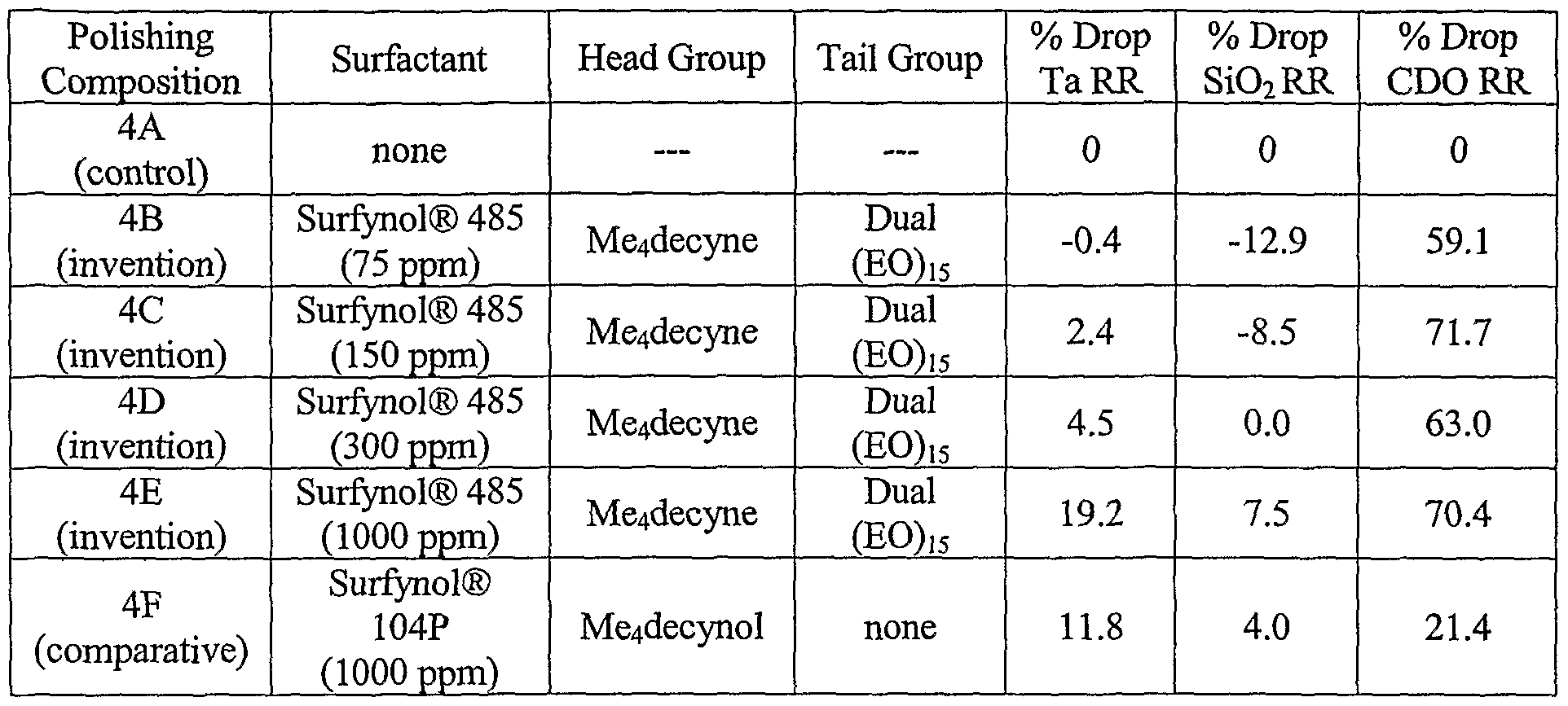
- EXAMPLE 4 [0047] This example illustrates the benefit of amphiphilic nonionic surfactants containing one head group and two tail groups on the substrate removal selectivity of low-k dielectric constant material removal in comparison to the removal rates of tantalum and silicon dioxide materials.
- polishing Compositions 4A-4F Similar substrates containing tantalum, silicon dioxide, and carbon-doped silicon dioxide (CDO) layers were polished with different polishing compositions (Polishing Compositions 4A-4F). Each of the polishing compositions contained 7 wt.% colloidal silica and 0.02 wt.% benzotriazole at a pH of 8. Polishing Composition 4A (control) contained no surfactant. Polishing Compositions 4B-4E (invention) contained 75, 150, 300, and 1000 ppm 2,4,7,9-tetramethyl-5-decyne-4,7-diol ethoxylate (30) (Surfynol® 485 surfactant, Air Products) having an HLB value of 17, respectively.
- Polishing Composition 4F contained 200 ppm 2,4,7,9-tetramethyl-5-decyne-4,7-diol (Surfynol® 104PA surfactant, Air Products) having an HLB value of 4.
- EXAMPLE 5 This example illustrates the benefit of amphiphilic nonionic surfactants on the substrate removal selectivity of low-k dielectric constant material removal in comparison to the removal rate of tantalum and silicon dioxide materials.
- polishing Compositions 5A-5K Similar blanket wafer substrates containing tantalum, silicon dioxide, or carbon-doped silicon dioxide (CDO) layers were polishing with different polishing compositions (Polishing Compositions 5A-5K). Each of the polishing compositions contained 12 wt.% abrasive, 0.02 wt.% benzotriazole, and 167 ppm surfactant and had a pH of 10. Polishing Composition 5 A (comparative) contained polyethylene glycol having a molecular weight of 600 (EO ⁇ ).
- Polishing Compositions 5B-5F each contained triblock copolymers of polyoxyethylene and polyoxypropylene (EO/PO/EO), specifically EO 20 -PO 70 -EO 20) EOi-PO ⁇ -EO,, EO ⁇ 3 -PO 30 -EO] 3 , EO 76 -PO 29 -EO 6 , and EOi 1-PO16-EO11, respectively.
- Polishing Compositions 5G-5I each contained block copolymers of polyethylene and polyoxyethylene, specifically PE ⁇ 2 -EO , PE 8 -EO ⁇ 0 , and PE 8 -EO ⁇ , respectively.
- Polishing Compositions 5J and 5K contained octylphenyl polyoxyethylene and octylcyclohexyl polyoxyethylene (Triton® X-100 and Triton® X-100R surfactants, Union Carbide), respectively.
- octylphenyl polyoxyethylene and octylcyclohexyl polyoxyethylene Triton® X-100 and Triton® X-100R surfactants, Union Carbide
Abstract
Description


Claims
Priority Applications (5)
| Application Number | Priority Date | Filing Date | Title |
|---|---|---|---|
| AU2003274812A AU2003274812A1 (en) | 2002-06-07 | 2003-05-26 | Method for chemical mechanical polishing (cmp) of low-k dielectric materials |
| DE60307111T DE60307111T2 (en) | 2002-06-07 | 2003-05-26 | METHOD FOR CHEMICAL MECHANICAL POLISHING OF MATERIALS WITH A LOW DIELECTRIC CONSTANT |
| EP03740859A EP1534795B1 (en) | 2002-06-07 | 2003-05-26 | Method for chemical mechanical polishing (cmp) of low-k dielectric materials |
| JP2004511407A JP4773091B2 (en) | 2002-06-07 | 2003-05-26 | CMP composition for low-k insulating materials |
| SG2004071809A SG108491A1 (en) | 2002-06-07 | 2003-05-26 | Method for chemical mechanical polishing (cmp) of low-k dielectric materials |
Applications Claiming Priority (2)
| Application Number | Priority Date | Filing Date | Title |
|---|---|---|---|
| US10/165,100 | 2002-06-07 | ||
| US10/165,100 US6974777B2 (en) | 2002-06-07 | 2002-06-07 | CMP compositions for low-k dielectric materials |
Publications (2)
| Publication Number | Publication Date |
|---|---|
| WO2003104343A2 true WO2003104343A2 (en) | 2003-12-18 |
| WO2003104343A3 WO2003104343A3 (en) | 2004-02-26 |
Family
ID=29710360
Family Applications (1)
| Application Number | Title | Priority Date | Filing Date |
|---|---|---|---|
| PCT/IB2003/002266 WO2003104343A2 (en) | 2002-06-07 | 2003-05-26 | Method for chemical mechanical polishing (cmp) of low-k dielectric materials |
Country Status (11)
| Country | Link |
|---|---|
| US (1) | US6974777B2 (en) |
| EP (1) | EP1534795B1 (en) |
| JP (1) | JP4773091B2 (en) |
| KR (1) | KR100729331B1 (en) |
| CN (1) | CN1305984C (en) |
| AT (1) | ATE334176T1 (en) |
| AU (1) | AU2003274812A1 (en) |
| DE (1) | DE60307111T2 (en) |
| SG (1) | SG108491A1 (en) |
| TW (1) | TWI227728B (en) |
| WO (1) | WO2003104343A2 (en) |
Cited By (5)
| Publication number | Priority date | Publication date | Assignee | Title |
|---|---|---|---|---|
| JP2005322670A (en) * | 2004-05-06 | 2005-11-17 | Mitsui Chemicals Inc | Polishing slurry |
| JP2006196887A (en) * | 2004-12-22 | 2006-07-27 | Rohm & Haas Electronic Materials Cmp Holdings Inc | Selective slurry for chemical mechanical polishing |
| JP2006269908A (en) * | 2005-03-25 | 2006-10-05 | Tmp Co Ltd | Chemical mechanical polishing slurry |
| US7161247B2 (en) | 2004-07-28 | 2007-01-09 | Cabot Microelectronics Corporation | Polishing composition for noble metals |
| WO2010011080A2 (en) * | 2008-07-24 | 2010-01-28 | 테크노세미켐 주식회사 | Chemical mechanical polishing composition containing polysilicon polish finisher |
Families Citing this family (89)
| Publication number | Priority date | Publication date | Assignee | Title |
|---|---|---|---|---|
| US5759917A (en) * | 1996-12-30 | 1998-06-02 | Cabot Corporation | Composition for oxide CMP |
| US7348300B2 (en) * | 1999-05-04 | 2008-03-25 | Air Products And Chemicals, Inc. | Acetylenic diol ethylene oxide/propylene oxide adducts and processes for their manufacture |
| US7208049B2 (en) * | 2003-10-20 | 2007-04-24 | Air Products And Chemicals, Inc. | Process solutions containing surfactants used as post-chemical mechanical planarization treatment |
| US6936543B2 (en) * | 2002-06-07 | 2005-08-30 | Cabot Microelectronics Corporation | CMP method utilizing amphiphilic nonionic surfactants |
| US6905974B2 (en) * | 2002-08-08 | 2005-06-14 | Micron Technology, Inc. | Methods using a peroxide-generating compound to remove group VIII metal-containing residue |
| US7077975B2 (en) * | 2002-08-08 | 2006-07-18 | Micron Technology, Inc. | Methods and compositions for removing group VIII metal-containing materials from surfaces |
| TWI256971B (en) * | 2002-08-09 | 2006-06-21 | Hitachi Chemical Co Ltd | CMP abrasive and method for polishing substrate |
| WO2004023539A1 (en) * | 2002-09-06 | 2004-03-18 | Asahi Glass Company, Limited | Polishing agent composition for insulating film for semiconductor integrated circuit and method for manufacturing semiconductor integrated circuit |
| US6893476B2 (en) * | 2002-12-09 | 2005-05-17 | Dupont Air Products Nanomaterials Llc | Composition and associated methods for chemical mechanical planarization having high selectivity for metal removal |
| US20040144038A1 (en) * | 2002-12-09 | 2004-07-29 | Junaid Ahmed Siddiqui | Composition and associated method for oxide chemical mechanical planarization |
| US7553345B2 (en) * | 2002-12-26 | 2009-06-30 | Kao Corporation | Polishing composition |
| US20050097825A1 (en) * | 2003-11-06 | 2005-05-12 | Jinru Bian | Compositions and methods for a barrier removal |
| US20050121969A1 (en) * | 2003-12-04 | 2005-06-09 | Ismail Emesh | Lubricant for wafer polishing using a fixed abrasive pad |
| JP2006016438A (en) * | 2004-06-30 | 2006-01-19 | Dongwoo Fine-Chem Co Ltd | Electronic part-washing liquid |
| US6979252B1 (en) | 2004-08-10 | 2005-12-27 | Dupont Air Products Nanomaterials Llc | Low defectivity product slurry for CMP and associated production method |
| PT1805452E (en) * | 2004-09-29 | 2014-05-07 | Koninkl Philips Nv | Lighting device |
| US7563383B2 (en) * | 2004-10-12 | 2009-07-21 | Cabot Mircroelectronics Corporation | CMP composition with a polymer additive for polishing noble metals |
| US7524347B2 (en) * | 2004-10-28 | 2009-04-28 | Cabot Microelectronics Corporation | CMP composition comprising surfactant |
| US7208325B2 (en) * | 2005-01-18 | 2007-04-24 | Applied Materials, Inc. | Refreshing wafers having low-k dielectric materials |
| US20070039926A1 (en) * | 2005-08-17 | 2007-02-22 | Cabot Microelectronics Corporation | Abrasive-free polishing system |
| US20070077865A1 (en) * | 2005-10-04 | 2007-04-05 | Cabot Microelectronics Corporation | Method for controlling polysilicon removal |
| US7265055B2 (en) * | 2005-10-26 | 2007-09-04 | Cabot Microelectronics Corporation | CMP of copper/ruthenium substrates |
| WO2007055278A1 (en) * | 2005-11-11 | 2007-05-18 | Hitachi Chemical Co., Ltd. | Polishing agent for silicon oxide, liquid additive, and method of polishing |
| KR100643632B1 (en) * | 2005-12-23 | 2006-11-10 | 제일모직주식회사 | Composition of slurry for polishing silicon wafer and method of polishing using thereby |
| JP2007184395A (en) * | 2006-01-06 | 2007-07-19 | Fujifilm Corp | Polishing liquid for metal |
| JP2007214155A (en) * | 2006-02-07 | 2007-08-23 | Fujifilm Corp | Polishing fluid for barrier, and chemical mechanical polishing method |
| US7442323B2 (en) * | 2006-06-02 | 2008-10-28 | E. I. Du Pont De Nemours And Company | Potassium monopersulfate solutions |
| US7678700B2 (en) * | 2006-09-05 | 2010-03-16 | Cabot Microelectronics Corporation | Silicon carbide polishing method utilizing water-soluble oxidizers |
| US9129907B2 (en) * | 2006-09-08 | 2015-09-08 | Cabot Microelectronics Corporation | Onium-containing CMP compositions and methods of use thereof |
| CN101153206A (en) * | 2006-09-29 | 2008-04-02 | 安集微电子(上海)有限公司 | Chemical mechanical polishing solution for polishing polysilicon |
| US20080105652A1 (en) * | 2006-11-02 | 2008-05-08 | Cabot Microelectronics Corporation | CMP of copper/ruthenium/tantalum substrates |
| US7456107B2 (en) * | 2006-11-09 | 2008-11-25 | Cabot Microelectronics Corporation | Compositions and methods for CMP of low-k-dielectric materials |
| JP2008130988A (en) * | 2006-11-24 | 2008-06-05 | Fujimi Inc | Polishing composition and polishing method |
| US20080148652A1 (en) * | 2006-12-21 | 2008-06-26 | Junaid Ahmed Siddiqui | Compositions for chemical mechanical planarization of copper |
| US20080149591A1 (en) * | 2006-12-21 | 2008-06-26 | Junaid Ahmed Siddiqui | Method and slurry for reducing corrosion on tungsten during chemical mechanical polishing |
| US20080148649A1 (en) * | 2006-12-21 | 2008-06-26 | Zhendong Liu | Ruthenium-barrier polishing slurry |
| US20080149884A1 (en) * | 2006-12-21 | 2008-06-26 | Junaid Ahmed Siddiqui | Method and slurry for tuning low-k versus copper removal rates during chemical mechanical polishing |
| JP5371207B2 (en) * | 2007-06-08 | 2013-12-18 | 富士フイルム株式会社 | Polishing liquid and polishing method |
| US8008202B2 (en) * | 2007-08-01 | 2011-08-30 | Cabot Microelectronics Corporation | Ruthenium CMP compositions and methods |
| US7915071B2 (en) * | 2007-08-30 | 2011-03-29 | Dupont Air Products Nanomaterials, Llc | Method for chemical mechanical planarization of chalcogenide materials |
| US20090124173A1 (en) * | 2007-11-09 | 2009-05-14 | Cabot Microelectronics Corporation | Compositions and methods for ruthenium and tantalum barrier cmp |
| JP2009164186A (en) * | 2007-12-28 | 2009-07-23 | Fujimi Inc | Polishing composition |
| JP5220428B2 (en) * | 2008-02-01 | 2013-06-26 | 株式会社フジミインコーポレーテッド | Polishing method using polishing composition |
| US8741008B2 (en) * | 2008-02-18 | 2014-06-03 | Jsr Corporation | Aqueous dispersion for chemical mechanical polishing and chemical mechanical polishing method |
| KR101202720B1 (en) * | 2008-02-29 | 2012-11-19 | 주식회사 엘지화학 | Aqueous slurry composition for chemical mechanical polishing and chemical mechanical polishing method |
| US8058183B2 (en) * | 2008-06-23 | 2011-11-15 | Applied Materials, Inc. | Restoring low dielectric constant film properties |
| JP5467804B2 (en) * | 2008-07-11 | 2014-04-09 | 富士フイルム株式会社 | Polishing liquid for silicon nitride and polishing method |
| US8247327B2 (en) * | 2008-07-30 | 2012-08-21 | Cabot Microelectronics Corporation | Methods and compositions for polishing silicon-containing substrates |
| CN102150242B (en) * | 2008-09-08 | 2013-05-15 | 三菱瓦斯化学株式会社 | Liquid for protecting copper wiring surface and method for manufacturing semiconductor circuit element |
| US20100081279A1 (en) * | 2008-09-30 | 2010-04-01 | Dupont Air Products Nanomaterials Llc | Method for Forming Through-base Wafer Vias in Fabrication of Stacked Devices |
| JP5362319B2 (en) * | 2008-10-21 | 2013-12-11 | 花王株式会社 | Polishing liquid composition |
| US8506661B2 (en) * | 2008-10-24 | 2013-08-13 | Air Products & Chemicals, Inc. | Polishing slurry for copper films |
| CN102482555B (en) * | 2009-06-22 | 2015-05-06 | 嘉柏微电子材料股份公司 | Cmp compositions and methods for suppressing polysilicon removal rates |
| EP2507824A4 (en) * | 2009-11-30 | 2013-09-25 | Basf Se | Process for removing a bulk material layer from a substrate and a chemical mechanical polishing agent suitable for this process |
| US8916473B2 (en) | 2009-12-14 | 2014-12-23 | Air Products And Chemicals, Inc. | Method for forming through-base wafer vias for fabrication of stacked devices |
| KR101782184B1 (en) * | 2009-12-22 | 2017-09-26 | 이시하라 산교 가부시끼가이샤 | Lithium titanate, manufacturing method therefor, slurry used in said manufacturing method, electrode active material containing said lithium titanate, and lithium secondary battery using said electrod active material |
| JP5587620B2 (en) * | 2010-01-25 | 2014-09-10 | 株式会社フジミインコーポレーテッド | Polishing composition and polishing method using the same |
| JP5492603B2 (en) * | 2010-03-02 | 2014-05-14 | 株式会社フジミインコーポレーテッド | Polishing composition and polishing method using the same |
| JP6101421B2 (en) * | 2010-08-16 | 2017-03-22 | インテグリス・インコーポレーテッド | Etching solution for copper or copper alloy |
| CN102399494B (en) * | 2010-09-10 | 2014-12-31 | 安集微电子(上海)有限公司 | Chemical mechanical polishing solution |
| RU2589482C2 (en) * | 2010-10-07 | 2016-07-10 | Басф Се | Aqueous polishing composition and method for chemical-mechanical polishing of substrates, having structured or unstructured dielectric layers with low dielectric constant |
| TWI565770B (en) * | 2010-10-07 | 2017-01-11 | 巴斯夫歐洲公司 | Aqueous polishing composition and process for chemically mechanically polishing substrates having patterned of unpatterned low-k dielectric layers |
| KR101919750B1 (en) | 2010-12-10 | 2018-11-19 | 바스프 에스이 | Aqueous polishing composition and process for chemically mechanically polishing substrates containing silicon oxide dielectric and polysilicon films |
| US9496146B2 (en) | 2011-03-11 | 2016-11-15 | Basf Se | Method for forming through-base wafer vias |
| EP2568024A1 (en) | 2011-09-07 | 2013-03-13 | Basf Se | A chemical mechanical polishing (cmp) composition comprising a glycoside |
| US9487674B2 (en) | 2011-09-07 | 2016-11-08 | Basf Se | Chemical mechanical polishing (CMP) composition comprising a glycoside |
| TWI456013B (en) * | 2012-04-10 | 2014-10-11 | Uwiz Technology Co Ltd | Polishing slurry composition |
| US9633863B2 (en) | 2012-07-11 | 2017-04-25 | Cabot Microelectronics Corporation | Compositions and methods for selective polishing of silicon nitride materials |
| US20140054266A1 (en) * | 2012-08-24 | 2014-02-27 | Wiechang Jin | Compositions and methods for selective polishing of platinum and ruthenium materials |
| EP2952550A4 (en) * | 2013-02-01 | 2016-09-28 | Fujimi Inc | Surface-selective polishing composition |
| US9284472B2 (en) | 2013-08-09 | 2016-03-15 | Fujimi Incorporated | SiCN and SiN polishing slurries and polishing methods using the same |
| US9281210B2 (en) | 2013-10-10 | 2016-03-08 | Cabot Microelectronics Corporation | Wet-process ceria compositions for polishing substrates, and methods related thereto |
| WO2016031485A1 (en) * | 2014-08-29 | 2016-03-03 | 株式会社フジミインコーポレーテッド | Polishing composition and method for producing polishing composition |
| KR102380774B1 (en) | 2014-11-14 | 2022-04-04 | 삼성전자주식회사 | Slurry compound and method of manufacturing semiconductor device using the same |
| CN107001916B (en) * | 2014-12-05 | 2019-01-22 | 3M创新有限公司 | Abrasive composition |
| CN105619267B (en) * | 2016-03-01 | 2018-02-02 | 中国科学院微电子研究所 | A kind of design method for polishing particle, polishing particle and lapping liquid |
| WO2018125905A1 (en) * | 2016-12-30 | 2018-07-05 | Fujifilm Planar Solutions, LLC | Polishing compositions |
| US10181408B2 (en) | 2017-01-31 | 2019-01-15 | Rohm And Haas Electronic Materials Cmp Holdings, Inc. | Chemical mechanical polishing method for tungsten using polyglycols and polyglycol derivatives |
| KR20190074597A (en) * | 2017-12-20 | 2019-06-28 | 주식회사 케이씨텍 | Polishing slurry composition for sti process |
| JP7316797B2 (en) | 2018-09-04 | 2023-07-28 | 株式会社フジミインコーポレーテッド | Polishing composition and polishing system |
| US11260420B2 (en) * | 2018-10-17 | 2022-03-01 | Portland State University | Nanowires with magnetic coatings and methods for making and using |
| KR102279324B1 (en) * | 2018-12-21 | 2021-07-21 | 주식회사 케이씨텍 | Polishing slurry composition |
| US11001733B2 (en) * | 2019-03-29 | 2021-05-11 | Fujimi Incorporated | Compositions for polishing cobalt and low-K material surfaces |
| CN113661563A (en) * | 2019-04-02 | 2021-11-16 | 昭和电工材料株式会社 | Polishing liquid, polishing liquid set, polishing method, and defect suppressing method |
| US10787592B1 (en) * | 2019-05-16 | 2020-09-29 | Rohm And Haas Electronic Materials Cmp Holdings, I | Chemical mechanical polishing compositions and methods having enhanced defect inhibition and selectively polishing silicon nitride over silicon dioxide in an acid environment |
| JP7340969B2 (en) | 2019-06-28 | 2023-09-08 | 東京応化工業株式会社 | Silicon etching solution, silicon etching method, and silicon fin structure manufacturing method |
| JP2022550331A (en) * | 2019-09-24 | 2022-12-01 | フジフイルム エレクトロニック マテリアルズ ユー.エス.エー., インコーポレイテッド | Polishing composition and method of use thereof |
| KR102637819B1 (en) * | 2020-03-31 | 2024-02-16 | 삼성에스디아이 주식회사 | Cmp slurry composition for polishing tungsten pattern wafer and method for polishing tungsten pattern wafer using the same |
| WO2023186762A1 (en) | 2022-03-31 | 2023-10-05 | Basf Se | Compositions and methods for tungsten etching inhibition |
Citations (4)
| Publication number | Priority date | Publication date | Assignee | Title |
|---|---|---|---|---|
| EP1088869A1 (en) * | 1999-09-30 | 2001-04-04 | JSR Corporation | Aqueous dispersion for chemical mechanical polishing |
| WO2001032794A1 (en) * | 1999-11-04 | 2001-05-10 | Advanced Micro Devices, Inc. | A ta barrier slurry containing an organic additive |
| EP1148538A1 (en) * | 1998-12-25 | 2001-10-24 | Hitachi Chemical Company, Ltd. | Cmp abrasive, liquid additive for cmp abrasive and method for polishing substrate |
| US20010054706A1 (en) * | 1999-07-19 | 2001-12-27 | Joseph A. Levert | Compositions and processes for spin etch planarization |
Family Cites Families (47)
| Publication number | Priority date | Publication date | Assignee | Title |
|---|---|---|---|---|
| US4752628A (en) * | 1987-05-15 | 1988-06-21 | Nalco Chemical Company | Concentrated lapping slurries |
| US4867757A (en) * | 1988-09-09 | 1989-09-19 | Nalco Chemical Company | Lapping slurry compositions with improved lap rate |
| US5352277A (en) * | 1988-12-12 | 1994-10-04 | E. I. Du Pont De Nemours & Company | Final polishing composition |
| US5123958A (en) * | 1990-05-25 | 1992-06-23 | Wiand Ronald C | Polishing composition and method |
| AU648704B2 (en) * | 1991-11-25 | 1994-04-28 | National Starch And Chemical Investment Holding Corporation | Method of extruding starch under low moisture conditions using feed starch having coarse particle size |
| TW274625B (en) * | 1994-09-30 | 1996-04-21 | Hitachi Seisakusyo Kk | |
| US5527423A (en) * | 1994-10-06 | 1996-06-18 | Cabot Corporation | Chemical mechanical polishing slurry for metal layers |
| US5860848A (en) * | 1995-06-01 | 1999-01-19 | Rodel, Inc. | Polishing silicon wafers with improved polishing slurries |
| US5958794A (en) * | 1995-09-22 | 1999-09-28 | Minnesota Mining And Manufacturing Company | Method of modifying an exposed surface of a semiconductor wafer |
| US6420269B2 (en) * | 1996-02-07 | 2002-07-16 | Hitachi Chemical Company, Ltd. | Cerium oxide abrasive for polishing insulating films formed on substrate and methods for using the same |
| ES2160892T3 (en) | 1996-05-30 | 2001-11-16 | Nalco Chemical Co | USE OF A TENSIOACTIVE MIX TO INHIBIT CORROSION. |
| US6117783A (en) * | 1996-07-25 | 2000-09-12 | Ekc Technology, Inc. | Chemical mechanical polishing composition and process |
| US6132637A (en) * | 1996-09-27 | 2000-10-17 | Rodel Holdings, Inc. | Composition and method for polishing a composite of silica and silicon nitride |
| US5876490A (en) * | 1996-12-09 | 1999-03-02 | International Business Machines Corporatin | Polish process and slurry for planarization |
| US6153525A (en) * | 1997-03-13 | 2000-11-28 | Alliedsignal Inc. | Methods for chemical mechanical polish of organic polymer dielectric films |
| JP2001522316A (en) * | 1997-04-18 | 2001-11-13 | キャボット マイクロエレクトロニクス コーポレイション | Polishing pad for semiconductor substrate |
| US6126532A (en) * | 1997-04-18 | 2000-10-03 | Cabot Corporation | Polishing pads for a semiconductor substrate |
| US6099604A (en) * | 1997-08-21 | 2000-08-08 | Micron Technology, Inc. | Slurry with chelating agent for chemical-mechanical polishing of a semiconductor wafer and methods related thereto |
| JP3371775B2 (en) * | 1997-10-31 | 2003-01-27 | 株式会社日立製作所 | Polishing method |
| US6063306A (en) * | 1998-06-26 | 2000-05-16 | Cabot Corporation | Chemical mechanical polishing slurry useful for copper/tantalum substrate |
| US6117000A (en) * | 1998-07-10 | 2000-09-12 | Cabot Corporation | Polishing pad for a semiconductor substrate |
| TW455626B (en) * | 1998-07-23 | 2001-09-21 | Eternal Chemical Co Ltd | Chemical mechanical abrasive composition for use in semiconductor processing |
| US6270395B1 (en) * | 1998-09-24 | 2001-08-07 | Alliedsignal, Inc. | Oxidizing polishing slurries for low dielectric constant materials |
| JP2000109816A (en) * | 1998-10-05 | 2000-04-18 | Okamoto Machine Tool Works Ltd | Preparation of polishing agent slurry |
| SG78405A1 (en) * | 1998-11-17 | 2001-02-20 | Fujimi Inc | Polishing composition and rinsing composition |
| US6046112A (en) * | 1998-12-14 | 2000-04-04 | Taiwan Semiconductor Manufacturing Company | Chemical mechanical polishing slurry |
| KR100472882B1 (en) * | 1999-01-18 | 2005-03-07 | 가부시끼가이샤 도시바 | Aqueous Dispersion, Chemical Mechanical Polishing Aqueous Dispersion Composition, Wafer Surface Polishing Process and Manufacturing Process of a Semiconductor Apparatus |
| US6426295B1 (en) * | 1999-02-16 | 2002-07-30 | Micron Technology, Inc. | Reduction of surface roughness during chemical mechanical planarization(CMP) |
| EP1171906A1 (en) | 1999-02-18 | 2002-01-16 | Rodel Holdings, Inc. | Method for cmp of low dielectric constant polymer layers |
| US20010013507A1 (en) * | 1999-02-18 | 2001-08-16 | Hosali Sharath D. | Method for CMP of low dielectric constant polymer layers |
| US6375693B1 (en) * | 1999-05-07 | 2002-04-23 | International Business Machines Corporation | Chemical-mechanical planarization of barriers or liners for copper metallurgy |
| JP2001015462A (en) * | 1999-06-30 | 2001-01-19 | Toshiba Corp | Slurry, cmp method and production of semiconductor device |
| US6376381B1 (en) * | 1999-08-31 | 2002-04-23 | Micron Technology, Inc. | Planarizing solutions, planarizing machines, and methods for mechanical and/or chemical-mechanical planarization of microelectronic substrate assemblies |
| TW499471B (en) * | 1999-09-01 | 2002-08-21 | Eternal Chemical Co Ltd | Chemical mechanical/abrasive composition for semiconductor processing |
| US6258140B1 (en) * | 1999-09-27 | 2001-07-10 | Fujimi America Inc. | Polishing composition |
| US6348076B1 (en) * | 1999-10-08 | 2002-02-19 | International Business Machines Corporation | Slurry for mechanical polishing (CMP) of metals and use thereof |
| JP3841995B2 (en) * | 1999-12-28 | 2006-11-08 | Necエレクトロニクス株式会社 | Chemical mechanical polishing slurry |
| JP3490038B2 (en) * | 1999-12-28 | 2004-01-26 | Necエレクトロニクス株式会社 | Metal wiring formation method |
| TW572980B (en) * | 2000-01-12 | 2004-01-21 | Jsr Corp | Aqueous dispersion for chemical mechanical polishing and chemical mechanical polishing process |
| JP4001219B2 (en) * | 2000-10-12 | 2007-10-31 | Jsr株式会社 | Chemical mechanical polishing aqueous dispersion and chemical mechanical polishing method |
| JP2001269859A (en) * | 2000-03-27 | 2001-10-02 | Jsr Corp | Aqueous dispersing element for polishing chemical machine |
| CN1175401C (en) * | 2000-04-28 | 2004-11-10 | 三井金属矿业株式会社 | Method for producing glass base plate for magnetic recording carrier |
| KR100481651B1 (en) * | 2000-08-21 | 2005-04-08 | 가부시끼가이샤 도시바 | Slurry for chemical mechanical polishing and method for manufacturing semiconductor device |
| JP4253141B2 (en) * | 2000-08-21 | 2009-04-08 | 株式会社東芝 | Chemical mechanical polishing slurry and semiconductor device manufacturing method |
| JP3768401B2 (en) * | 2000-11-24 | 2006-04-19 | Necエレクトロニクス株式会社 | Chemical mechanical polishing slurry |
| JP2002161267A (en) * | 2000-11-27 | 2002-06-04 | Hitachi Chem Co Ltd | Polishing liquid for platinum group metal and method for polishing with the same |
| JP4009986B2 (en) * | 2000-11-29 | 2007-11-21 | 株式会社フジミインコーポレーテッド | Polishing composition and polishing method for polishing memory hard disk using the same |
-
2002
- 2002-06-07 US US10/165,100 patent/US6974777B2/en not_active Expired - Lifetime
-
2003
- 2003-05-26 JP JP2004511407A patent/JP4773091B2/en not_active Expired - Fee Related
- 2003-05-26 CN CNB038131722A patent/CN1305984C/en not_active Expired - Lifetime
- 2003-05-26 AU AU2003274812A patent/AU2003274812A1/en not_active Abandoned
- 2003-05-26 KR KR1020047019821A patent/KR100729331B1/en active IP Right Grant
- 2003-05-26 EP EP03740859A patent/EP1534795B1/en not_active Expired - Lifetime
- 2003-05-26 WO PCT/IB2003/002266 patent/WO2003104343A2/en active IP Right Grant
- 2003-05-26 AT AT03740859T patent/ATE334176T1/en not_active IP Right Cessation
- 2003-05-26 DE DE60307111T patent/DE60307111T2/en not_active Expired - Lifetime
- 2003-05-26 SG SG2004071809A patent/SG108491A1/en unknown
- 2003-06-06 TW TW092115419A patent/TWI227728B/en not_active IP Right Cessation
Patent Citations (4)
| Publication number | Priority date | Publication date | Assignee | Title |
|---|---|---|---|---|
| EP1148538A1 (en) * | 1998-12-25 | 2001-10-24 | Hitachi Chemical Company, Ltd. | Cmp abrasive, liquid additive for cmp abrasive and method for polishing substrate |
| US20010054706A1 (en) * | 1999-07-19 | 2001-12-27 | Joseph A. Levert | Compositions and processes for spin etch planarization |
| EP1088869A1 (en) * | 1999-09-30 | 2001-04-04 | JSR Corporation | Aqueous dispersion for chemical mechanical polishing |
| WO2001032794A1 (en) * | 1999-11-04 | 2001-05-10 | Advanced Micro Devices, Inc. | A ta barrier slurry containing an organic additive |
Non-Patent Citations (1)
| Title |
|---|
| MCCLATCHIE S ET AL: "LOW DIELECTRIC CONSTANT OXIDE FILMS DEPOSITED USING CVD TECHNIQUES" DUMIC CONFERENCE PROCEEDINGS, XX, XX, February 1998 (1998-02), pages 311-318, XP000866192 * |
Cited By (7)
| Publication number | Priority date | Publication date | Assignee | Title |
|---|---|---|---|---|
| JP2005322670A (en) * | 2004-05-06 | 2005-11-17 | Mitsui Chemicals Inc | Polishing slurry |
| US7161247B2 (en) | 2004-07-28 | 2007-01-09 | Cabot Microelectronics Corporation | Polishing composition for noble metals |
| JP2006196887A (en) * | 2004-12-22 | 2006-07-27 | Rohm & Haas Electronic Materials Cmp Holdings Inc | Selective slurry for chemical mechanical polishing |
| JP2006269908A (en) * | 2005-03-25 | 2006-10-05 | Tmp Co Ltd | Chemical mechanical polishing slurry |
| WO2010011080A2 (en) * | 2008-07-24 | 2010-01-28 | 테크노세미켐 주식회사 | Chemical mechanical polishing composition containing polysilicon polish finisher |
| WO2010011080A3 (en) * | 2008-07-24 | 2010-05-14 | 테크노세미켐 주식회사 | Chemical mechanical polishing composition containing polysilicon polish finisher |
| KR101094662B1 (en) * | 2008-07-24 | 2011-12-20 | 솔브레인 주식회사 | Chemical mechanical polishing composition including a stopping agent of poly-silicon polishing |
Also Published As
| Publication number | Publication date |
|---|---|
| DE60307111T2 (en) | 2006-11-23 |
| CN1659249A (en) | 2005-08-24 |
| AU2003274812A8 (en) | 2003-12-22 |
| SG108491A1 (en) | 2007-01-31 |
| JP4773091B2 (en) | 2011-09-14 |
| ATE334176T1 (en) | 2006-08-15 |
| TWI227728B (en) | 2005-02-11 |
| DE60307111D1 (en) | 2006-09-07 |
| KR20050005543A (en) | 2005-01-13 |
| WO2003104343A3 (en) | 2004-02-26 |
| EP1534795A2 (en) | 2005-06-01 |
| US20030228762A1 (en) | 2003-12-11 |
| EP1534795B1 (en) | 2006-07-26 |
| JP2005529485A (en) | 2005-09-29 |
| TW200401819A (en) | 2004-02-01 |
| CN1305984C (en) | 2007-03-21 |
| US6974777B2 (en) | 2005-12-13 |
| AU2003274812A1 (en) | 2003-12-22 |
| KR100729331B1 (en) | 2007-06-15 |
Similar Documents
| Publication | Publication Date | Title |
|---|---|---|
| US6974777B2 (en) | CMP compositions for low-k dielectric materials | |
| KR101201115B1 (en) | Cmp method utilizing amphiphilic non-ionic surfactants | |
| KR101092939B1 (en) | Composition for polishing semiconductor layers | |
| CN105219274B (en) | Compositions and methods for chemical mechanical polishing of low dielectric constant dielectric materials | |
| JP4814784B2 (en) | Modular barrier removal polishing slurry | |
| KR101472617B1 (en) | Polishing liquid for metal and method of polishing | |
| US20080105652A1 (en) | CMP of copper/ruthenium/tantalum substrates | |
| EP1685202A1 (en) | Chemical-mechanical polishing composition and method for using the same | |
| KR20100067610A (en) | Chemical mechanical polishing composition and methods relating thereto | |
| US6682575B2 (en) | Methanol-containing silica-based CMP compositions |
Legal Events
| Date | Code | Title | Description |
|---|---|---|---|
| AK | Designated states |
Kind code of ref document: A2 Designated state(s): AE AG AL AM AT AU AZ BA BB BG BR BY BZ CA CH CN CO CR CU CZ DE DK DM DZ EC EE ES FI GB GD GE GH GM HR HU ID IL IN IS JP KE KG KP KR KZ LC LK LR LS LT LU LV MA MD MG MK MN MW MX MZ NI NO NZ OM PH PL PT RO RU SC SD SE SG SK SL TJ TM TN TR TT TZ UA UG UZ VC VN YU ZA ZM ZW |
|
| AL | Designated countries for regional patents |
Kind code of ref document: A2 Designated state(s): GH GM KE LS MW MZ SD SL SZ TZ UG ZM ZW AM AZ BY KG KZ MD RU TJ TM AT BE BG CH CY CZ DE DK EE ES FI FR GB GR HU IE IT LU MC NL PT RO SE SI SK TR BF BJ CF CG CI CM GA GN GQ GW ML MR NE SN TD TG |
|
| 121 | Ep: the epo has been informed by wipo that ep was designated in this application | ||
| DFPE | Request for preliminary examination filed prior to expiration of 19th month from priority date (pct application filed before 20040101) | ||
| WWE | Wipo information: entry into national phase |
Ref document number: 1020047019821 Country of ref document: KR |
|
| WWE | Wipo information: entry into national phase |
Ref document number: 20038131722 Country of ref document: CN Ref document number: 2004511407 Country of ref document: JP |
|
| WWE | Wipo information: entry into national phase |
Ref document number: 2003740859 Country of ref document: EP |
|
| WWP | Wipo information: published in national office |
Ref document number: 1020047019821 Country of ref document: KR |
|
| WWP | Wipo information: published in national office |
Ref document number: 2003740859 Country of ref document: EP |
|
| WWG | Wipo information: grant in national office |
Ref document number: 2003740859 Country of ref document: EP |