WO2011019017A1 - Electronic device, signal transmission device, and signal transmission method - Google Patents
Electronic device, signal transmission device, and signal transmission method Download PDFInfo
- Publication number
- WO2011019017A1 WO2011019017A1 PCT/JP2010/063485 JP2010063485W WO2011019017A1 WO 2011019017 A1 WO2011019017 A1 WO 2011019017A1 JP 2010063485 W JP2010063485 W JP 2010063485W WO 2011019017 A1 WO2011019017 A1 WO 2011019017A1
- Authority
- WO
- WIPO (PCT)
- Prior art keywords
- transmission
- signal
- reception
- unit
- electronic device
- Prior art date
Links
Images


Classifications
-
- H—ELECTRICITY
- H04—ELECTRIC COMMUNICATION TECHNIQUE
- H04B—TRANSMISSION
- H04B7/00—Radio transmission systems, i.e. using radiation field
- H04B7/02—Diversity systems; Multi-antenna system, i.e. transmission or reception using multiple antennas
- H04B7/022—Site diversity; Macro-diversity
-
- H—ELECTRICITY
- H04—ELECTRIC COMMUNICATION TECHNIQUE
- H04B—TRANSMISSION
- H04B7/00—Radio transmission systems, i.e. using radiation field
- H04B7/02—Diversity systems; Multi-antenna system, i.e. transmission or reception using multiple antennas
- H04B7/04—Diversity systems; Multi-antenna system, i.e. transmission or reception using multiple antennas using two or more spaced independent antennas
- H04B7/0413—MIMO systems
Definitions
- the present invention relates to an electronic device, a signal transmission device, and a signal transmission method. More specifically, the present invention relates to signal distribution, switching, and signal aggregation (aggregation).
- LVDS Low Voltage Differential Signaling
- LVDS Low Voltage Differential Signaling
- a relatively short distance for example, within several centimeters to several tens of centimeters.
- problems such as an increase in power consumption, an increase in the influence of signal distortion due to reflection, an increase in unnecessary radiation, and the like.
- LVDS has reached its limit when signals such as video signals (including imaging signals) and computer images are transmitted at high speed (in real time) within the device.
- Japanese Patent Application Laid-Open No. 2005-204221 and Japanese Patent Application Laid-Open No. 2005-223411 propose to perform signal transmission in a housing wirelessly and to apply a UWB (Ultra Wide Band) communication method.
- the UWB communication systems in these two patent documents have a problem of size such as a low carrier frequency, which is not suitable for high-speed communication such as transmitting a video signal, and an antenna becomes large. Further, since the frequency used for transmission is close to the frequency of other baseband signal processing, there is a problem that interference easily occurs between the radio signal and the baseband signal. Further, when the carrier frequency is low, it is easily affected by drive system noise in the device, and it is necessary to deal with it.
- Japanese Patent Application Laid-Open No. 10-256478 and US Pat. No. 5,754,948 describe that a carrier frequency in the millimeter wave band is used.
- a carrier frequency in a millimeter wave band with a shorter wavelength when used, problems of antenna size, interference, and drive system noise can be solved.
- JP 2005-204221 A Japanese Patent Laid-Open No. 2005-223411 JP-A-10-256478 US Pat. No. 5,754,948
- signal distribution for transmitting the same signal to multiple locations
- signal switching for transmitting one signal to any of multiple locations
- Signal aggregation may be performed.
- circuits called dividers and analog switches are used, but the design of electrical wiring (including printed wiring board patterns) becomes more difficult, and the circuit and its surroundings This causes problems such as an increase in the number of parts and an increase in wiring. In order to take this measure, the circuit becomes more complicated.
- an object of the present invention is to provide an invention that can perform signal distribution, signal switching, and signal aggregation with a simpler configuration.
- the signal transmission device includes a pre-stage signal processing unit that performs predetermined signal processing on a transmission target signal, and a modulation unit that modulates a processed signal output from the pre-stage signal processing unit
- a transmitter that transmits the signal modulated by the modulator as a radio signal
- a receiver that receives the radio signal transmitted from the transmitter
- a demodulator that demodulates the signal received by the receiver
- a post-stage signal processing unit that performs predetermined signal processing on the received signal is disposed at a predetermined location in the housing.
- a wireless signal transmission path that enables wireless transmission is formed between a transmission position of the wireless signal in the transmission section and a reception position of the wireless signal in the reception section, and the transmission position and the reception position of one wireless signal transmission path are formed.
- a plurality of communication paths can be formed.
- a radio signal transmission location and a radio signal transmitted from the transmission unit are transmitted in a transmission unit that transmits a signal processed signal for a transmission target signal as a radio signal. It is possible to form a plurality of communication paths between radio signal reception locations in the receiving unit for receiving.
- the signal distribution which distributes the same transmission object signal to a plurality of receiving parts by transmitting the same radio signal transmitted from one transmitting point to a plurality of receiving points using a plurality of communication paths, Signal switching for switching the transmission destination of a transmission target signal using a communication path, and transmission of a plurality of transmission target signals by transmitting each wireless signal transmitted from a plurality of transmission positions to a single reception position using each communication path Execute at least one of signal concentration for concentrating the signal to one receiver.
- the electronic apparatus according to the third aspect of the present invention applies the “signal distribution” in the signal transmission apparatus according to the first aspect of the present invention and the signal transmission method according to the second aspect of the present invention. It is.
- the electronic apparatus according to the fourth aspect of the present invention applies the “signal switching” in the signal transmission apparatus according to the first aspect of the present invention and the signal transmission method according to the second aspect of the present invention. It is.
- An electronic apparatus according to the fifth aspect of the present invention applies the “signal set” in the signal transmission apparatus according to the first aspect of the present invention and the signal transmission method according to the second aspect of the present invention. It is.
- the electronic device according to the third aspect of the present invention, the electronic device according to the fourth aspect, and the electronic device according to the fifth aspect all transmit a transmission target signal as a radio signal.
- the receiver and the receiver that receives the wireless signal transmitted from the transmitter are arranged in the housing, and wireless transmission is possible between the transmission point of the wireless signal in the transmitter and the reception point of the wireless signal in the receiver
- a wireless signal transmission path is formed, and a plurality of communication paths between a transmission point and a reception point can be formed in one wireless signal transmission line.
- the same transmission is transmitted by transmitting the same radio signal transmitted from one transmission location to a plurality of reception locations using a plurality of communication paths.
- Signal distribution for distributing the target signal to a plurality of receiving units can be executed.
- signal switching for switching the transmission destination of the transmission target signal can be performed using a plurality of communication paths.
- a plurality of transmission target signals are transmitted by transmitting each wireless signal transmitted from a plurality of transmission locations to one reception location using each communication path. It is possible to perform signal concentration for concentrating the signals to one receiving unit.
- Each electronic device described in the dependent claims of the electronic device according to the third aspect, the fourth aspect, and the fifth aspect of the present invention includes the third aspect, the fourth aspect, and the A further advantageous specific example of the electronic device according to the fifth aspect is defined.
- the signal transmission device according to the first aspect of the present invention and the signal transmission method according to the second aspect of the present invention are provided.
- Various techniques and methods applied to each electronic device described in the dependent claims of the electronic device according to the aspect are also applicable.
- the transmission target signal is transmitted as a radio signal.
- signal distribution, signal switching, and signal aggregation are realized using radio signals by a plurality of communication paths. Since there is no portion for signal transmission by electrical wiring in the portion of the communication path that realizes signal distribution, signal switching, and signal collection, signal distribution, signal switching, and signal collection can be performed with a simple configuration.
- signal distribution, signal switching, and signal aggregation can be performed with a simple configuration.
- FIG. 1 is a diagram of a reference configuration for explaining the signal interface of the signal transmission apparatus according to the present embodiment from the functional configuration side.
- FIG. 2 is a first basic configuration for explaining the signal interface of the signal transmission apparatus according to the present embodiment in terms of functional configuration.
- FIG. 3 shows a second basic configuration for explaining the signal interface of the signal transmission apparatus according to the present embodiment in terms of functional configuration.
- FIG. 4 shows a third basic configuration for explaining the signal interface of the signal transmission apparatus according to the present embodiment in terms of functional configuration.
- FIG. 5A and FIG. 5B are diagrams for explaining the signal interface of the signal transmission device of the comparative example from the functional configuration side.
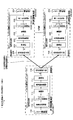
- FIG. 6 is a diagram illustrating an overall configuration of the first embodiment.
- FIG. 6 is a diagram illustrating an overall configuration of the first embodiment.
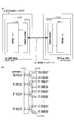
- FIG. 7 is a diagram illustrating a pair of transmission / reception systems in the overall configuration of the first embodiment.
- FIG. 8 is a diagram showing a signal processing system on the transmission side and a signal processing system on the reception side.
- FIG. 9 is a diagram illustrating an example of antenna directivity.
- FIG. 10 is a diagram illustrating an overall configuration of the second embodiment.
- FIG. 11A to FIG. 11C are diagrams for explaining the concept of space division multiplexing adopted in the second embodiment.
- FIG. 12 is a diagram for explaining the third embodiment.
- FIG. 13 is a diagram for explaining the fourth embodiment.
- FIG. 14 is a diagram for explaining the fifth embodiment.
- FIG. 15 is a diagram for explaining the sixth embodiment.
- FIG. 16 is a diagram for explaining the seventh embodiment.
- FIG. 17 is a diagram for explaining the eighth embodiment.
- FIG. 18 is a diagram for explaining the ninth embodiment.
- FIG. 19 is a diagram for explaining the tenth embodiment.
- 20A and 20B are diagrams illustrating a first example of an electronic apparatus according to the eleventh embodiment.
- FIGS. 21A to 21C are diagrams illustrating a second example of the electronic apparatus according to the eleventh embodiment.
- 22A to 22C are diagrams illustrating a third example of the electronic apparatus according to the eleventh embodiment.
- Communication processing system Reference configuration
- Communication processing system Basic configuration 1 to basic configuration 3 4).
- Example 1 Application example of first basic configuration
- Example 2 Application of space division multiplexing
- Example 3 One signal is generated on the receiving side based on a plurality of signals.
- Example 4 A plurality of methods for processing a signal acquired by one electronic device on the receiving side.
- Example 5 Signal switching by relative movement between transmission and reception ⁇ application to a rotating structure
- Modifications Examples 6 to 10 (Modifications of Examples 1 to 5)
- Ten Example 11: Application to electronic equipment
- the transmission unit for example, transmission-side coupling unit on the transmission side
- the reception unit for example, transmission-line coupling unit on the reception side
- the transmission unit transmits the transmission target signal as a radio signal.
- the receiving unit receives the radio signal transmitted from the transmitting unit.
- At least one of the preceding stage of the transmitting unit and the subsequent stage of the receiving unit is further provided with a signal processing unit.
- the signal processing unit performs predetermined signal processing.
- a pre-stage signal processing unit that performs predetermined signal processing on a transmission target signal and a modulation unit that modulates a processed signal output from the pre-stage signal processing unit are provided.
- a demodulator that demodulates the signal received by the receiver, and a subsequent signal processor that performs predetermined signal processing on the signal demodulated by the demodulator are provided.
- a plurality of communication paths can be formed between a transmission position of the wireless signal in the transmission section and a reception position of the wireless signal in the reception section, and the same wireless signal transmitted from one transmission position using the plurality of communication paths
- Signal distribution that distributes the same transmission target signal to multiple reception units by transmitting the signal to multiple reception locations using multiple communication paths, and the transmission destination of the transmission target signal using multiple communication paths
- Signal switching for switching and at least one of signal concentrations for concentrating a plurality of transmission target signals on one receiving unit by transmitting each wireless signal transmitted from a plurality of transmitting locations to one receiving location using each communication path Make one executable.
- the basic configuration for signal distribution, signal switching, or signal aggregation is as follows: 1-to-N configuration, M-to-1 configuration, or Any of an M-to-N configuration can be taken.
- a so-called 1-to-N configuration in which a plurality of reception locations are arranged for one transmission location can be employed. That is, by arranging a plurality of reception locations for one transmission location, a plurality of communication paths can be arranged between the transmission location and the reception location. And the signal distribution which transmits the transmission object signal transmitted from one transmission location to a some reception location is enabled.
- a so-called M-to-N configuration in which a plurality of reception locations are arranged with respect to a plurality of transmission locations can be adopted. That is, by arranging a plurality of reception locations for a plurality of transmission locations, a plurality of communication paths can be arranged between the transmission location and the reception location. And the signal distribution which transmits the same transmission object signal transmitted from either of a some transmission location to a some reception location is enabled.
- a so-called 1-to-N configuration in which a plurality of reception locations are arranged with respect to one transmission location can be adopted. That is, by arranging a plurality of reception locations for one transmission location, a plurality of communication paths can be arranged between the transmission location and the reception location. Then, signal switching for selectively transmitting a transmission target signal transmitted from one transmission location to any of a plurality of reception locations can be executed.
- a so-called M-to-1 configuration in which one reception location is arranged for a plurality of transmission locations can be adopted. That is, a plurality of communication paths can be arranged between a transmission location and a reception location by arranging one reception location for a plurality of transmission locations. Then, it is possible to execute signal switching for selectively transmitting any of the transmission target signals transmitted from any of the plurality of transmission locations to one reception location.
- a so-called M-to-N configuration in which a plurality of reception locations are arranged with respect to a plurality of transmission locations can be adopted. That is, by arranging a plurality of reception locations for a plurality of transmission locations, a plurality of communication paths can be arranged between the transmission location and the reception location. Then, it is possible to perform signal switching for selectively transmitting a transmission target signal transmitted from any of the plurality of transmission locations to any of the plurality of reception locations.
- a so-called M-to-1 configuration in which one reception location is arranged for a plurality of transmission locations can be adopted. That is, a plurality of communication paths can be arranged between a transmission location and a reception location by arranging one reception location for a plurality of transmission locations. Then, it is possible to execute a signal set in which transmission target signals transmitted from each of a plurality of transmission locations are collected into one reception location.
- a so-called M-to-N configuration in which a plurality of reception locations are arranged with respect to a plurality of transmission locations can be adopted. That is, by arranging a plurality of reception locations for a plurality of transmission locations, a plurality of communication paths can be arranged between the transmission location and the reception location. Then, for at least one of the plurality of reception points, a signal set in which transmission target signals transmitted from the plurality of transmission points are collected into one reception point can be executed.
- the interval between the transmission location and the reception location (distance between channels: typically the distance between antennas) as follows so that signal transmission is performed simultaneously. That is, the interval between the transmission location and the reception location is within a range where the same transmission target signal transmitted from the transmission location can be received simultaneously at a plurality of reception locations, or a plurality of transmission target signals can be simultaneously received at one reception location. And set within the receivable range.
- the transmitting side transmits information for identifying the receiving location where the transmission target signal transmitted from the transmitting location is to be received together with the transmission target signal, and the receiving side identifies the receiving location. Based on the information, it may be controlled whether to receive and demodulate the transmission target signal transmitted from the transmission location.
- the transmission location and the reception location may be relatively movable.
- the antenna on the transmission side or the reception side on the wireless (electromagnetic wave) transmission path is moved, or the transmission side Further, the electronic device can be easily switched by moving the electronic device on the receiving side.
- a plurality of multiplexing schemes such as frequency division multiplexing and code division multiplexing are applied.
- a radio signal transmission path between a transmission location and a reception location may be configured to transmit a radio signal while confining the radio signal in the transmission path.
- the radio signal transmission path between the transmission location and the reception location is a free space that does not have a structure for transmitting the radio signal while confining the radio signal in the transmission path, and between the pair of the adjacent transmission location and the reception location.
- the distance may be set so that independent communication between adjacent neighbors is possible (that is, no interference or interference occurs).
- a space and a structure for inserting a transmitting antenna or a receiving antenna are provided for a wireless transmission path between a combination of a wireless transmitter and a transmitting antenna and a combination of a wireless receiver and a receiving antenna. It is preferable to enable signal transmission with other wireless transmitters and wireless receivers added by inserting the.
- a plurality of pairs capable of forming a plurality of pairs of wireless signal transmission locations and reception portions of wireless signals in the reception portion are provided, and signal processing is performed using signals acquired in the respective pairs.
- signal processing is performed using signals acquired in the respective pairs.
- one signal may be generated using signals acquired in each set.
- a plurality of pairs capable of forming a plurality of pairs of wireless signal transmission locations and reception portions of wireless signals in the reception portion are provided, and signal distribution, signal switching, or signal collection is performed in each pair.
- signals having different characteristics may be acquired by performing signal processing with different characteristics based on radio signals emitted from the same transmission location.
- each part is housed in a single casing.
- One electronic device may be configured, or an entire electronic device may be configured by a combination of a plurality of devices (electronic devices).
- the signal transmission device (wireless transmission device) of this embodiment is used in electronic devices such as a digital recording / reproducing device, a terrestrial television receiver, a mobile phone device, a game device, and a computer.
- the signal transmission apparatus In the signal transmission device of the present embodiment described below, it is assumed that a carrier frequency in the millimeter wave band (wavelength is 1 to 10 mm) is used.
- the signal transmission apparatus is not limited to the millimeter wave band, and has a shorter wavelength, for example, a submillimeter wave. It is also applicable when using a carrier frequency near the millimeter wave band such as a band.
- a signal transmission device When configuring a signal transmission device, there are cases where the transmission side is alone, reception side alone, and both transmission side and reception side.
- the transmitting side and the receiving side are coupled via a radio signal transmission path (for example, a millimeter wave signal transmission path) and configured to perform signal transmission in the millimeter wave band.
- a signal to be transmitted is frequency-converted to a millimeter wave band suitable for wideband transmission and transmitted.
- a signal transmission device is configured by a first communication unit (first millimeter wave transmission device) and a second communication unit (second millimeter wave transmission device).
- wireless transmission in the present embodiment means that a signal to be transmitted is transmitted wirelessly (in this example, millimeter wave) instead of general electrical wiring (simple wire wiring).
- “Relatively close distance” means that the distance is shorter than the distance between communication devices in the outdoors (outdoors) used in broadcasting and general wireless communication, and the transmission range is closed. As long as it can be substantially specified.
- “Closed space” means a space where there is little leakage of radio waves from the inside of the space to the outside, and conversely, there is little arrival (intrusion) of radio waves from the outside to the inside of the space. The entire space is surrounded by a casing (case) that has a shielding effect against radio waves.
- a plurality of electronic devices are integrated, such as inter-board communication within a housing of one electronic device, inter-chip communication on the same substrate, or a state in which the other electronic device is mounted on one electronic device.
- the “integrated” is typically a state in which both electronic devices are completely in contact with each other, but it may be of a level that can be substantially specified as a space in which the transmission range between the two electronic devices is closed.
- both electronic devices are arranged at a predetermined position in a relatively short distance, such as within a few centimeters or within a few tens of centimeters, can be regarded as being “substantially” integral.
- signal transmission within a casing of one electronic device is referred to as signal transmission within the casing, and signal transmission in a state in which a plurality of electronic devices are integrated (hereinafter also including “substantially integrated”) is performed.
- This is called inter-signal transmission.
- the communication device on the transmission side communication unit: transmission unit
- the communication device on the reception side communication unit: reception unit
- a signal transmission device in which a wireless signal transmission path is formed becomes an electronic device itself.
- the communication device on the transmission side (communication unit: transmission unit) and the communication device on the reception side (communication unit: reception unit) are accommodated in different electronic device casings, and both electronic devices are A radio signal transmission path is formed between communication units (transmission unit and reception unit) in both electronic devices when they are arranged at a predetermined position and integrated with each other, thereby constructing a signal transmission device.
- each communication device provided across the millimeter wave signal transmission path, a transmission system and a reception system are paired and arranged. Two-way communication can be performed by causing each communication device to have both a transmission system and a reception system.
- signal transmission between one communication device and the other communication device may be one-way (one-way) or two-way.
- the transmission unit is arranged in the first communication unit and the reception unit is arranged in the second communication unit.
- the transmission unit is arranged in the second communication unit and the reception unit is arranged in the first communication unit.
- the transmission unit includes, for example, a transmission-side signal generation unit (a signal conversion unit that converts a transmission target electric signal into a millimeter wave signal) that processes a transmission target signal to generate a millimeter wave signal, and a millimeter wave It is assumed that a transmission-side signal coupling unit that couples a millimeter-wave signal generated by the transmission-side signal generation unit to a transmission path (millimeter-wave signal transmission path) for transmitting the above signal is provided.
- the signal generator on the transmission side is integrated with a functional unit that generates a signal to be transmitted.
- the signal generator on the transmission side has a modulation circuit, and the modulation circuit modulates a signal to be transmitted.
- the signal generator on the transmission side converts the frequency of the signal after being modulated by the modulation circuit to generate a millimeter wave signal.
- a signal to be transmitted may be directly converted into a millimeter wave signal.
- the signal coupling unit on the transmission side supplies the millimeter wave signal generated by the signal generation unit on the transmission side to the millimeter wave signal transmission path.
- the receiving unit includes, for example, a receiving-side signal coupling unit that receives a millimeter-wave signal transmitted via the millimeter-wave signal transmission path, and a millimeter-wave signal (input signal) received by the receiving-side signal coupling unit.
- a receiving-side signal coupling unit that receives a millimeter-wave signal transmitted via the millimeter-wave signal transmission path, and a millimeter-wave signal (input signal) received by the receiving-side signal coupling unit.
- a reception-side signal generation unit a signal conversion unit that converts a millimeter-wave signal into a transmission target electrical signal.
- the signal generation unit on the reception side is integrated with a function unit that receives a signal to be transmitted.
- the signal generation unit on the reception side includes a demodulation circuit, generates an output signal by frequency-converting a millimeter wave signal, and then the demodulation circuit generates a signal to be transmitted by demodulating the output signal.
- a millimeter wave signal may be directly converted to a transmission target signal.
- the signal to be transmitted is transmitted by a millimeter wave signal without contact or cable (not by electrical wiring).
- at least signal transmission (especially a video signal or high-speed clock signal that requires high-speed transmission or large-capacity transmission) is transmitted by a millimeter wave signal.
- signal transmission that has been performed by electrical wiring in the past is performed by a millimeter wave signal in this embodiment.
- each signal coupling unit may be any unit that enables the first communication unit and the second communication unit to transmit a millimeter-wave signal via the millimeter-wave signal transmission path.
- it may be provided with an antenna structure (antenna coupling portion), or may be coupled without an antenna structure.
- the “millimeter wave signal transmission path for transmitting a millimeter wave signal” may be air (so-called free space), but preferably has a structure for transmitting a millimeter wave signal while confining the millimeter wave signal in the transmission path ( It is preferable to have a millimeter wave confinement structure or a radio signal confinement structure.
- a typical example of such a millimeter-wave confinement structure is a so-called waveguide, but is not limited thereto.
- a dielectric material capable of transmitting a millimeter wave signal referred to as a dielectric transmission line or an in-millimeter wave dielectric transmission line
- a shield that constitutes a transmission line and suppresses external radiation of the millimeter wave signal.
- a hollow waveguide in which the material is provided so as to surround the transmission path and the inside of the shielding material is hollow is preferable.
- the millimeter wave signal transmission path can be routed by providing flexibility to the dielectric material and the shielding material.
- each signal coupling portion has an antenna structure, and signals are transmitted in a short-distance space by the antenna structure.
- an antenna structure can be taken, but this is not essential.
- the setting values that define the operation of the signal processing unit can be preset or statically controlled. . Since the set value prescribes the operation of the signal processing unit appropriately, high-quality communication is possible while having a simple configuration and low power consumption.
- the following advantages can be obtained by using wireless communication in the millimeter-wave band with a short wavelength.
- the frequency used for transmission can be separated from the frequency of other baseband signal processing, and interference between the millimeter wave and the frequency of the baseband signal hardly occurs.
- a highly stable external frequency reference component In order to realize such a highly stable carrier wave, a highly stable external frequency reference component, a multiplier circuit, a PLL (phase locked loop circuit), and the like are used, which increases the circuit scale.
- millimeter waves can be easily shielded (especially when used in combination with signal transmission between fixed positions or with a known positional relationship) and can be prevented from leaking outside.
- an injection locking method In order to demodulate a signal transmitted by a carrier wave having a low stability with a small circuit on the receiving side, it is preferable to adopt an injection locking method.
- LVDS Low Voltage Differential Signaling
- EMI problem EMI problem
- LVDS has reached its limit when signals such as video signals (including image pickup signals) and computer images are transmitted at high speed (in real time) within a device or between devices.
- the number of wires may be increased and the transmission speed per signal line may be reduced by parallelizing signals.
- this countermeasure leads to an increase in input / output terminals.
- it is required to increase the complexity of the printed circuit board and the cable wiring and to increase the semiconductor chip size.
- so-called electromagnetic field interference becomes a problem when high-speed and large-capacity data is routed by wiring.
- any problems in the LVDS and the method of increasing the number of wirings are caused by transmitting signals through electrical wiring. Therefore, as a technique for solving the problems caused by transmitting signals through the electrical wiring, a technique of transmitting the electrical wiring wirelessly may be employed.
- a method of transmitting electrical wiring by wireless for example, the signal transmission in the housing is performed wirelessly, and a UWB (Ultra Wide Band) communication method may be applied (referred to as the first method), or the wavelength A short (1-10 mm) millimeter-wave band carrier frequency may be used (referred to as the second technique).
- the UWB communication method of the first method has a problem in size such as a low carrier frequency, which is not suitable for high-speed communication for transmitting a video signal, for example, and an antenna becomes large. Further, since the frequency used for transmission is close to the frequency of other baseband signal processing, there is a problem that interference easily occurs between the radio signal and the baseband signal. Further, when the carrier frequency is low, it is easily affected by drive system noise in the device, and it is necessary to deal with it. On the other hand, when the carrier frequency in the millimeter wave band having a shorter wavelength is used as in the second method, problems of antenna size and interference can be solved.
- the application range is not limited to that in which communication is performed in the millimeter wave band.
- Communication in a frequency band below the millimeter wave band, or conversely, in a frequency band exceeding the millimeter wave band may be applied.
- a submillimeter wave band having a shorter wavelength (0.1 to 1 mm) than a microwave band or millimeter wave band may be applied.
- FIG. 1 is a diagram for explaining the signal interface of the signal transmission apparatus according to the present embodiment in terms of functional configuration, and is a reference configuration for basic configurations 1 to 3 to be described later.
- This reference configuration is a one-to-one signal transmission device 1 with one transmission system and one reception system, and signals using wireless communication (wireless signal transmission) adopted in basic configurations 1 to 3 described later.
- functions of signal distribution, signal switching, and signal aggregation are realized by wireless communication using a functional portion for performing wireless communication provided in the reference configuration shown here.
- the signal transmission device 1 includes a first communication device 100, which is an example of a first wireless device, and a second communication device 200, which is an example of a second wireless device, coupled via a millimeter wave signal transmission path 9 to the millimeter wave band. Is configured to perform signal transmission.
- a transmission system is provided on the first communication device 100 side, and a reception system is provided on the second communication device 200.
- the first communication device 100 is provided with a semiconductor chip 103 corresponding to millimeter wave band transmission
- the second communication device 200 is provided with a semiconductor chip 203 corresponding to millimeter wave band reception.
- the signals to be communicated in the millimeter wave band are limited to signals that require high speed and large capacity, and other signals that can be regarded as direct current, such as those that are sufficient for low speed and small capacity, and power sources. Not converted to millimeter wave signal.
- signals including power supplies
- signals are connected between the substrates in the same manner as before.
- the original electrical signals to be transmitted before being converted into millimeter waves are collectively referred to as baseband signals.
- a semiconductor chip 103 that supports millimeter wave band transmission and a transmission path coupling unit 108 are mounted on a substrate 102.
- the semiconductor chip 103 is an LSI (Large Scale Integrated Circuit) in which an LSI function unit 104, which is an example of a pre-stage signal processing unit, and a signal generation unit 107 (millimeter wave signal generation unit) are integrated.
- LSI Large Scale Integrated Circuit
- the semiconductor chip 103 is connected to the transmission line coupling unit 108.
- the transmission line coupling unit 108 is an example of a transmission unit, and for example, an antenna structure including an antenna coupling unit, an antenna terminal, a microstrip line, an antenna, and the like is applied.
- a location where the transmission path coupling unit 108 and the millimeter wave signal transmission path 9 are coupled is a transmission location, and an antenna typically corresponds to a transmission location.
- the LSI function unit 104 controls the main application of the first communication device 100, and includes, for example, a circuit that processes various signals to be transmitted to the other party.
- the signal generation unit 107 (electrical signal conversion unit) converts a signal from the LSI function unit 104 into a millimeter wave signal and includes a transmission side signal generation unit 110 for performing signal transmission control via the millimeter wave signal transmission path 9.
- the transmission side signal generation unit 110 and the transmission path coupling unit 108 constitute a transmission system (transmission unit: transmission side communication unit).
- the transmission-side signal generation unit 110 includes a multiplexing processing unit 113, a parallel-serial conversion unit 114, a modulation unit 115, a frequency conversion unit 116, and an amplification unit 117 in order to perform signal processing on the input signal to generate a millimeter wave signal.
- the amplifying unit 117 is an example of an amplitude adjusting unit that adjusts and outputs the magnitude of an input signal. Note that the modulation unit 115 and the frequency conversion unit 116 may be combined into a so-called direct conversion system.
- the multiplexing processing unit 113 performs time division multiplexing, frequency division multiplexing, code processing, when there are a plurality of types (N1) of signals to be communicated in the millimeter wave band among the signals from the LSI function unit 104.
- multiplexing processing such as division multiplexing, a plurality of types of signals are combined into one system signal. For example, a plurality of types of signals that are required to be high speed and large capacity are collected into one system of signals as targets of transmission using millimeter waves.
- the parallel-serial conversion unit 114 converts a parallel signal into a serial data signal and supplies it to the modulation unit 115.
- the modulation unit 115 modulates the transmission target signal and supplies it to the frequency conversion unit 116.
- the parallel-serial conversion unit 114 is provided in the case of the parallel interface specification using a plurality of signals for parallel transmission when this embodiment is not applied, and is not required in the case of the serial interface specification.
- the modulation unit 115 may basically be any unit that modulates at least one of amplitude, frequency, and phase with a transmission target signal, and any combination of these may be employed.
- analog modulation methods include amplitude modulation (AM) and vector modulation, for example.
- Vector modulation includes frequency modulation (FM) and phase modulation (PM).
- AM amplitude modulation
- FM frequency modulation
- PM phase modulation
- ASK Amplitude shift keying
- FSK Frequency Shift Keying
- PSK Phase Shift Keying
- APSK Amplitude Phase Shift Keying
- amplitude phase modulation amplitude phase that modulates amplitude and phase
- APSK Amplitude Phase Shift Keying
- quadrature amplitude modulation QAM: Quadrature Amplitude Modulation
- a method that can adopt the synchronous detection method on the receiving side is adopted.
- the frequency conversion unit 116 converts the frequency of the transmission target signal after being modulated by the modulation unit 115 to generate a millimeter-wave electric signal, and supplies the generated signal to the amplification unit 117.
- a millimeter-wave electrical signal refers to an electrical signal having a frequency in the range of approximately 30 GHz to 300 GHz.
- the term “substantially” may be a frequency at which the effect of millimeter wave communication can be obtained, and the lower limit is not limited to 30 GHz, and the upper limit is not limited to 300 GHz.
- the frequency conversion unit 116 for example, a configuration including a frequency mixing circuit (mixer circuit) and a local oscillation circuit may be employed.
- the local oscillation circuit generates a carrier wave (carrier signal, reference carrier wave) used for modulation.
- the frequency mixing circuit multiplies (modulates) the millimeter-wave band carrier wave generated by the local oscillation circuit with the signal from the parallel-serial conversion unit 114 to generate a millimeter-wave band transmission signal and supplies it to the amplification unit 117.
- the amplifying unit 117 amplifies the millimeter-wave electrical signal after frequency conversion and supplies the amplified signal to the transmission line coupling unit 108.
- the amplifying unit 117 is connected to the bidirectional transmission line coupling unit 108 via an antenna terminal (not shown).
- the transmission path coupling unit 108 transmits the millimeter wave signal generated by the transmission side signal generation unit 110 to the millimeter wave signal transmission path 9.
- the transmission line coupling unit 108 includes an antenna coupling unit.
- the antenna coupling unit constitutes an example or a part of the transmission path coupling unit 108 (signal coupling unit).
- the antenna coupling part means a part for coupling an electronic circuit in a semiconductor chip and an antenna arranged inside or outside the chip in a narrow sense. In a broad sense, the antenna coupling part includes a semiconductor chip and a millimeter wave signal transmission line 9. This is the part where signals are combined.
- the antenna coupling unit includes at least an antenna structure.
- the antenna structure refers to a structure at a coupling portion with the millimeter wave signal transmission path 9 and may be anything that couples a millimeter wave band electrical signal to the millimeter wave signal transmission path 9 and does not mean only the antenna itself. .
- the millimeter wave signal transmission path 9 which is a millimeter wave propagation path may be configured as a free space transmission path that propagates in, for example, a space in a housing.
- it is composed of a waveguide structure such as a waveguide, a transmission line, a dielectric line, a dielectric body, etc., and has a characteristic of efficiently transmitting an electromagnetic wave in the millimeter wave band in a transmission line. It is desirable to do.
- the dielectric transmission line 9A may be configured to include a dielectric material having a specific dielectric constant in a certain range and a dielectric loss tangent in a certain range.
- a dielectric material 9A is disposed between the transmission line coupling unit 108 and the transmission line coupling unit 208 instead of the free space transmission line by filling a dielectric material throughout the housing.
- the dielectric transmission line 9A is connected by connecting the antenna of the transmission line coupling unit 108 and the antenna of the transmission line coupling unit 208 with a dielectric line which is a linear member having a certain wire diameter made of a dielectric material. May be configured.
- the millimeter wave signal transmission line 9 configured to confine the millimeter wave signal in the transmission line, in addition to the dielectric transmission line 9A, the transmission line may be surrounded by a shielding material and the inside thereof may be a hollow hollow waveguide. Good.
- a semiconductor chip 203 and a transmission path coupling unit 208 that support millimeter wave band reception are mounted on a substrate 202.
- the semiconductor chip 203 is an LSI in which an LSI function unit 204, which is an example of a post-stage signal processing unit, and a signal generation unit 207 (millimeter wave signal generation unit) are integrated.
- the LSI function unit 204 and the signal generation unit 207 may not be integrated.
- the semiconductor chip 203 is connected to a transmission line coupling unit 208 similar to the transmission line coupling unit 108.
- the transmission path coupling unit 208 is an example of a reception unit, and the same one as the transmission path coupling unit 108 is adopted.
- the transmission path coupling unit 208 receives a millimeter wave signal from the millimeter wave signal transmission path 9 and outputs it to the reception side signal generation unit 220. .
- the signal generation unit 207 (electric signal conversion unit) includes a reception-side signal generation unit 220 for performing signal reception control via the millimeter wave signal transmission path 9.
- the reception side signal generation unit 220 and the transmission path coupling unit 208 constitute a reception system (reception unit: reception side communication unit).
- a location where the transmission path coupling unit 208 and the millimeter wave signal transmission path 9 are coupled is a reception location, and typically an antenna corresponds to the reception location.
- the reception-side signal generation unit 220 performs signal processing on the millimeter-wave electrical signal received by the transmission path coupling unit 208 to generate an output signal, so that an amplification unit 224, a frequency conversion unit 225, a demodulation unit 226, serial parallel conversion A unit 227 and a unification processing unit 228.
- the amplifying unit 224 is an example of an amplitude adjusting unit that adjusts and outputs the magnitude of an input signal.
- the frequency converter 225 and the demodulator 226 may be combined into a so-called direct conversion system. Further, the demodulation carrier signal may be generated by applying an injection locking method.
- the transmission side signal generator 220 is connected to the transmission path coupler 208.
- the receiving-side amplifying unit 224 is connected to the transmission line coupling unit 208, amplifies the millimeter-wave electrical signal received by the antenna, and supplies the amplified signal to the frequency converting unit 225.
- the frequency converter 225 performs frequency conversion on the amplified millimeter-wave electrical signal and supplies the frequency-converted signal to the demodulator 226.
- the demodulator 226 demodulates the frequency-converted signal, acquires a baseband signal, and supplies the baseband signal to the serial-parallel converter 227.
- the serial / parallel conversion unit 227 converts serial reception data into parallel output data and supplies the parallel output data to the unification processing unit 228. Similar to the parallel-serial conversion unit 114, the serial-parallel conversion unit 227 is provided in the case of a parallel interface specification using a plurality of signals for parallel transmission when this embodiment is not applied. When the original signal transmission between the first communication device 100 and the second communication device 200 is in a serial format, the parallel / serial conversion unit 114 and the serial / parallel conversion unit 227 may not be provided.
- the input signal is parallel-serial converted and transmitted to the semiconductor chip 203 side, and received from the semiconductor chip 203 side.
- the number of signals subject to millimeter wave conversion is reduced by serial-parallel conversion of the signals.
- the unification processing unit 228 corresponds to the multiplexing processing unit 113, and separates signals collected in one system into a plurality of types of signals _ @ (@ is 1 to N). For example, a plurality of data signals collected in one system of signals are separated and supplied to the LSI function unit 204.
- the LSI function unit 204 is responsible for main application control of the second communication device 200, and includes, for example, a circuit for processing various signals received from the other party.
- the signal generation unit 107 and the transmission path coupling unit 108, and the signal generation unit 207 and the transmission path coupling unit 208 are configured to have bidirectional data so that bidirectional communication can be supported.
- the signal generation unit 107 and the signal generation unit 207 are each provided with a reception-side signal generation unit and a transmission-side signal generation unit.
- the transmission path coupling unit 108 and the transmission path coupling unit 208 may be provided separately on the transmission side and the reception side, but can also be used for transmission and reception.
- the millimeter-wave signal transmission path 9 which is a millimeter-wave transmission channel is one-line (one-core) single-core bidirectional transmission.
- TDD Time Division Duplex
- FDD frequency division multiplexing
- the signal generation unit 107 and the signal generation unit 207 used in the present embodiment are higher in frequency than the frequency used by complicated transmitters and receivers generally used in broadcasting and wireless communication. Since the wavelength ⁇ is short and the wavelength ⁇ is short, it is easy to reuse the frequency, and a device suitable for communication between many devices arranged in the vicinity is used.
- the signal transmission is performed in the millimeter wave band as described above, so that high speed and large capacity can be flexibly supported. For example, only signals that require high speed and large capacity are targeted for communication in the millimeter wave band.
- the first communication device 100 and the second communication device 200 may be used for low-speed and small-capacity signals.
- an interface (connection by a terminal / connector) using a conventional electric wiring is provided in part.
- the signal generation unit 107 is an example of a signal processing unit that performs predetermined signal processing based on a set value. In this example, the signal generation unit 107 performs signal processing on an input signal input from the LSI function unit 104 to perform a millimeter-wave signal. Is generated.
- the signal generation unit 107 is connected to the transmission line coupling unit 108 via a transmission line such as a microstrip line, a strip line, a coplanar line, or a slot line, and the generated millimeter wave signal is transmitted via the transmission line coupling unit 108. It is supplied to the millimeter wave signal transmission line 9.
- the transmission path coupling unit 108 has an antenna structure, and has a function of converting a transmitted millimeter wave signal into an electromagnetic wave and transmitting the electromagnetic wave.
- the transmission path coupling unit 108 is coupled to the millimeter wave signal transmission path 9, and an electromagnetic wave converted by the transmission path coupling unit 108 is supplied to one end of the millimeter wave signal transmission path 9.
- the other end of the millimeter wave signal transmission line 9 is coupled to the transmission line coupling unit 208 on the second communication device 200 side.
- the millimeter wave signal transmission line 9 By providing the millimeter wave signal transmission line 9 between the transmission line coupling unit 108 on the first communication device 100 side and the transmission line coupling unit 208 on the second communication device 200 side, the millimeter wave signal transmission line 9 has a millimeter wave band. Electromagnetic waves propagate.
- the millimeter wave signal transmission path 9 is coupled with a transmission path coupling unit 208 on the second communication device 200 side.
- the transmission path coupling unit 208 receives the electromagnetic wave transmitted to the other end of the millimeter wave signal transmission path 9, converts it to a millimeter wave signal, and supplies it to the signal generation unit 207 (baseband signal generation unit).
- the signal generation unit 207 is an example of a signal processing unit that performs predetermined signal processing based on a set value.
- the converted millimeter wave signal is signal-processed and output as an output signal (baseband signal). Is generated and supplied to the LSI function unit 204.
- the signal transmission from the first communication device 100 to the second communication device 200 has been described. However, by configuring the first communication device 100 and the second communication device 200 to support bidirectional communication, Similarly, when transmitting a signal from the LSI function unit 204 of the second communication device 200 to the first communication device 100, a millimeter-wave signal can be transmitted in both directions.
- FIG. 2 is a first basic configuration (basic configuration 1) for explaining the signal interface of the signal transmission apparatus of the present embodiment from the functional configuration aspect.
- the first basic configuration is a one-to-N signal transmission apparatus 1 having one transmission system and N reception systems, and a plurality of common radio signals transmitted from one transmission system (N Signal distribution function by (preferably demodulating) reception (preferably at the same time) reception systems and multiple (N) reception systems selected from one transmission system Thus, a signal switching function by receiving (more specifically, demodulating) is realized.
- N reception systems are configured by different semiconductor chips 203, these may be combined into one semiconductor chip, and the N signal generation units 207 may be connected to different semiconductor chips. It is possible to modify the N LSI functional units 204 as a single semiconductor chip while forming a chip. What is necessary is just to utilize what is called broadcast communication, when implement
- a frequency switching system, a code division multiplexing system, or the like can be applied, and control using identification information can be performed.
- the N reception systems may correspond to different carrier frequencies.
- One transmission system may be a wide-band transmission circuit corresponding to N types of carrier frequencies, and modulation may be performed with a modulated carrier signal having a carrier frequency corresponding to a destination to which a signal is to be transmitted.
- identification information for distinguishing N reception systems is included in the transmission data, and whether each reception system is addressed to itself is determined based on the identification information to determine whether to perform demodulation or subsequent signal processing. You may control.
- FIG. 3 shows a second basic configuration (basic configuration 2) for explaining the signal interface of the signal transmission device according to the present embodiment from the functional configuration aspect.
- the second basic configuration is an M-to-one signal transmission apparatus 1 with M transmission systems and one reception system, and wireless signals transmitted from a plurality (M) of transmission systems are 1
- the function of signal switching by selectively receiving (more specifically, demodulating) by one receiving system, and one receiving system collectively receiving radio signals transmitted from multiple (M) transmission systems
- the function of signal concentration (or signal aggregation) is realized by distinguishing and demodulating.
- the figure shows an example in which M transmission systems are configured by different semiconductor chips 103, but these may be combined into one semiconductor chip, and the M signal generation units 107 may be connected to different semiconductor chips.
- the M LSI function units 104 can be modified as a single semiconductor chip while forming a chip.
- a time division multiplexing system, a frequency division multiplexing system, a code division multiplexing system, or the like can be applied, and control using identification information can be performed.
- the M transmission systems correspond to the same carrier frequency, and each transmission system may perform transmission processing at different timings.
- identification information for distinguishing M transmission systems is included in transmission data.
- Applying frequency division multiplexing the M transmission systems correspond to different carrier frequencies, and one reception system is a wideband reception circuit corresponding to M types of carrier frequencies. You may demodulate separately.
- FIG. 4 shows a third basic configuration (basic configuration 3) for explaining the signal interface of the signal transmission apparatus according to the present embodiment from the functional configuration side.
- the third basic configuration is a combination of the first basic configuration and the second basic configuration.
- M transmission systems and N reception systems M and N may be the same number or different.
- a signal switching function by selectively receiving (more specifically, demodulating) one of a plurality of reception systems of radio signals transmitted from a plurality (M) of transmission systems.
- a signal concentration function is realized by receiving radio signals transmitted from a plurality (M) of transmission systems collectively by each reception system.
- M plurality of transmission systems collectively by each reception system.
- Each function can be applied in any combination.
- a time division multiplexing method, a frequency division multiplexing method, a code division multiplexing method, or the like can be applied, and control using identification information is performed. Can be done.
- FIG. 5 is a diagram for explaining the signal interface of the signal transmission device of the comparative example from the viewpoint of the functional configuration.
- FIG. 5A shows an overall outline thereof.
- the signal transmission device 1Z of the comparative example is configured such that the first device 100Z and the second device 200Z are coupled via the electrical interface 9Z to perform signal transmission.
- the first device 100Z is provided with a semiconductor chip 103Z capable of transmitting signals via electrical wiring
- the second device 200Z is also provided with a semiconductor chip 203Z capable of transmitting signals via electrical wiring.
- the millimeter wave signal transmission line 9 of the first embodiment is replaced with an electrical interface 9Z.
- the first device 100Z is provided with an electrical signal conversion unit 107Z in place of the signal generation unit 107 and the transmission path coupling unit 108, and the second device 200Z has a signal generation unit 207 and Instead of the transmission line coupling unit 208, an electric signal conversion unit 207Z is provided.
- the electrical signal conversion unit 107Z performs electrical signal transmission control on the LSI function unit 104 via the electrical interface 9Z.
- the electrical signal conversion unit 207Z is accessed via the electrical interface 9Z and obtains data transmitted from the LSI function unit 104 side.
- the solid-state imaging device is disposed in the vicinity of the optical lens, and various signal processing such as image processing, compression processing, and image storage of electrical signals from the solid-state imaging device.
- various signal processing such as image processing, compression processing, and image storage of electrical signals from the solid-state imaging device.
- a signal processing circuit outside the solid-state imaging device.
- LVDS is often used to deal with this. In order to transmit LVDS signals with high accuracy, matched impedance termination is required.
- Japanese Patent Laid-Open No. 2003-110919 proposes a mechanism for correcting camera shake by moving a solid-state imaging device, but the load of an actuator for deflecting a cable for transmitting an electric signal becomes a problem. .
- the load on the actuator is reduced by using wireless transmission.
- Generation of multi-view images (see Japanese Patent Application Laid-Open No. 09-27969) and three-dimensional moving image data require signals from a plurality of solid-state imaging devices and their processing. In this case, high-speed transmission within the device The number of transmission lines using the technology is further increased.
- a signal distribution IC (so-called divider IC), a signal switching IC (so-called switch IC), or the like is used in order to prevent deterioration in signal transmission quality.
- FIG. 5A shows a case where LVDS signals are distributed.
- n is the number of data
- the clock and data are assumed to be differential (complementary).
- the electric signal converter 107Z is provided with a signal distribution IC
- the electric signal converter 207Z is provided with two buffer ICs.
- the difficulty of designing the printed wiring board is further increased, and the number of integrated circuits for signal distribution and the peripheral parts and wiring are increased. Cause an increase problem.
- Japanese Patent Application Laid-Open No. 2009-27748 describes that communication using an electromagnetic wave transmission path is performed in an electronic device.
- it is necessary to easily divide the electromagnetic wave transmission path in order to avoid interference, and to distribute (branch) an electric signal. ) And signal switching are not mentioned.
- the electric signal conversion unit 107Z and the electric signal conversion unit 207Z of the comparative example are replaced with the signal generation unit 107, the signal generation unit 207, the transmission path coupling unit 108, and the like.
- the transmission line coupling unit 208 By replacing with the transmission line coupling unit 208, signal transmission is performed in the millimeter wave band (wireless) instead of electrical wiring.
- the signal transmission path is replaced by the electromagnetic wave transmission path from the wiring. For this reason, signal distribution can be realized using a so-called broadcast communication function, and signal switching can be realized using selective reception (demodulation), and signal distribution and signal switching can be performed with a simple configuration. .
- each embodiment described below is not limited to being applied alone, but can be applied in any combination within a possible range. Even if some constituent elements are deleted from all the constituent elements shown in the embodiment, as long as an effect is obtained, a configuration from which these several constituent elements are deleted can be extracted as an invention.
- a solid-state imaging device is used as an electronic device will be mainly described.
- this embodiment performs signal distribution and signal switching using wireless communication even in an electronic device using high-speed transfer technology other than the solid-state imaging device.
- the present invention can be applied to an image signal information transmission apparatus for connecting displays and a signal processing method thereof.
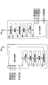
- FIG. 6 to 9 are diagrams for explaining the first embodiment.
- FIG. 6 is a diagram illustrating an overall configuration of the first embodiment
- FIG. 7 is a diagram illustrating a pair of transmission / reception systems in the overall configuration.
- FIG. 8 is a diagram showing a signal processing system on the transmission side and a signal processing system on the reception side.
- FIG. 9 is a diagram illustrating an example of antenna directivity.
- one pair of millimeter wave signal transmission lines 9 (wireless transmission lines) is adopted, the first basic configuration is adopted, and there is one transmission system and N reception systems. N signal transmission apparatuses 1 are applied.
- an electronic device 411 corresponding to the LSI function unit 104 such as a semiconductor integrated circuit or a solid-state imaging device is provided on the transmission side.
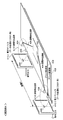
- the transmission antenna 436 (transmitter side antenna, transmission location) has a patch antenna, a loop antenna, a small aperture coupling element (slot antenna, etc.), etc. It is selected and used according to the directivity characteristics and the shape of the millimeter wave signal transmission line 9 to be generated.
- the installation location of the transmission antenna 436 is, for example, the back surface or the vicinity of the electronic device 411. The figure shows an example in which a dipole antenna is used as the transmission antenna 436 and is arranged on the back surface of the electronic device 411.
- the format of the antenna is, for example, an electronic device 411 (for example, a solid state) in addition to an antenna on a semiconductor package disclosed in Japanese Patent Laid-Open No. 2000-68904, an antenna formed on a single chip as disclosed in Japanese Patent Laid-Open No. 2003-101320
- a transmission antenna 436 may be formed on a printed wiring board on which the imaging device is mounted and connected to the electronic device 411. Or the form which connects the transmission antenna 436 and the electronic device 411 which were formed on the other printed wiring board can also be used.
- the size of the transmission antenna 436 is about 1 mm although it depends on the frequency used and the material around the antenna. This is a size that can be sufficiently installed on the back surface of the electronic device 411 (for example, a solid-state imaging device).
- N receiving antennas 446 receiving locations
- signal generating units 207 for N systems (four systems in the figure) in order to deal with 1-to-N signal distribution and signal switching.
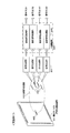
- the LSI function unit 204 is provided with N systems (four systems in the figure) of rear-stage signal processing units 448.
- the function of the subsequent signal processing unit 448 is set according to the demand of the user. For example, the signal from the solid-state imaging device is processed and colorized (for example, signal generation of three primary colors of red, blue, and green), compression processing for storing imaging data is performed, and HDMI (High-Definition Multimedia Interface) And processing such as conversion to a connection format to an external monitor represented by DVI (Digital Visual Interface).
- DVI Digital Visual Interface
- a differential (complementary) signal of one clock and data n (n is the number of data) is transmitted in the millimeter wave band via the millimeter wave signal transmission line 9.
- imaging data from the solid-state imaging device is represented by a clock and data synchronized therewith. This is processed in the transmission system by the signal generation unit 107 shown in FIG. 8 to be sent to the transmission antenna 436 in the millimeter wave band, and is output to the transmission antenna 436 via the transmission line coupling unit 108.
- a reception antenna 446 (a reception side antenna) is arranged on a millimeter wave signal transmission path 9 (electromagnetic wave transmission path) by a millimeter wave transmitted from the transmission side (for example, the solid-state imaging device side). 1 data and n data) are demodulated.
- the reception antenna 446 does not need to be on the same line as the transmission antenna 436 and does not need to be in the same aerial form as the transmission antenna 436 as long as the intensity of electromagnetic waves for reception is sufficiently obtained.
- reception processing is performed by the signal generation unit 207 shown in FIG. This makes it possible to transmit a large-capacity high-speed signal from the electronic device 411.
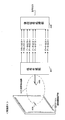
- FIG. 9 shows an example of the shape of a dipole antenna when a dipole antenna is used as an antenna format used in millimeter waves, and the directivity of a transmittable range of a millimeter wave signal radiated therefrom.
- the dipole antenna has directivity on the horizontal plane. Broadcast communication is realized by arranging a plurality of receiving antennas 446 (that is, each receiving point) within the transmission range of the transmitting antenna 436 including the directivity, and signal distribution that distributes the same signal to a plurality of locations is easy. To be realized.
- ⁇ Signal switching can also be realized by embedding a code for identifying the recipient in the transmission data so that one recipient can be specified from a plurality of recipients.
- the plurality of receiving antennas 446 are connected to a distance difference from the transmitting antenna 436 that does not hinder the simultaneous transmission of data. It is good to arrange within the range. That is, the interval between the transmission location and the reception location is set within a range in which the same transmission target signal transmitted from the transmission location can be received simultaneously at a plurality of reception locations.
- a space in which a receiving antenna is inserted into a transmission possible range between a combination of a millimeter wave band transmitter and a transmitting antenna and a combination of a millimeter wave receiver and a receiving antenna.
- the antenna is inserted into an electromagnetic wave transmission path (within the transmission range of the transmission antenna 436), and signal distribution, signal switching, and signal switching to other millimeter wave band receivers connected to the inserted antenna are performed. You can gather.
- the electronic device 411 solid-state imaging device or the like
- the high-speed transmission path is an electrical wiring
- an electrical contact is formed on the terminal of the electronic device 411 with a pin or the like and connected to an inspection device. Perform an inspection.
- the electronic device 411 is provided with the signal generation unit 107 and the transmission path coupling unit 108 (including the transmission antenna 436), the inspection is performed within the transmission possible range (electromagnetic wave transmission path) of the transmission antenna 436. By inserting this antenna, radio can be used for inspection, and electrical contact with the high-speed transmission path is not necessary. For this reason, the cost of inspection equipment can be reduced, and replacement of inspection equipment becomes easy.
- the electronic device 411 By putting a shielding object such as a metal between a plurality of electronic devices 411 (solid-state imaging device or the like) and switching the millimeter wave signal transmission path 9 (transmittable range of the transmission antenna 436) reaching the reception antenna 446, the electronic device 411 can also be switched.
- a shielding object such as a metal between a plurality of electronic devices 411 (solid-state imaging device or the like) and switching the millimeter wave signal transmission path 9 (transmittable range of the transmission antenna 436) reaching the reception antenna 446.
- the electronic device 411 and its electrical wiring could not be easily branched.
- signal distribution and switching can be performed only by providing the probe receiving antenna 446 within the transmittable range of the transmitting antenna 436.
- the signal output from the electronic device 411 can be observed with a measuring instrument or the like without changing the electrical wiring to isolate the location where the failure has occurred.
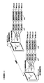
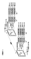
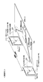
- FIG. 10 to 11 are diagrams for explaining the second embodiment.
- FIG. 10 is a diagram illustrating an overall configuration of the second embodiment
- FIG. 11 is a diagram illustrating the concept of space division multiplexing employed in the second embodiment.
- Example 2 is a case where a plurality of systems of 1 to N signal transmission apparatuses 1 (one adopting the first basic configuration) having one transmission system and N reception systems are provided.
- the electronic device 411 the LSI function unit 104 ⁇ the signal generation unit 107 ⁇ the transmission antenna 436 ⁇ the reception antenna 446 ⁇ the signal generation unit 207 ⁇ the LSI function unit 204 has a plurality of paths (two systems in the figure). Install.
- the M-to-2N signal transmission apparatus 1 which employs the third basic configuration
- 2N reception systems is employed.
- each system is the same as that described in the first embodiment.
- the shorter the inter-channel distance D typically, the distance between transmitting antennas
- the shorter the channel is formed by each transmitting antenna 436.
- the transmission possible range (transmission channel) will be close, and interference and interference on the receiving side may become a problem.
- Sharpening the antenna directivity leads to a reduction in the size of the reception antenna 446. This is one of the reasons for using the millimeter wave band.
- the arrangement of the transmitting antenna 436, the electromagnetic wave output intensity of the transmitting antenna 436, the arrangement of the receiving antenna 446, etc. avoid interference and interference even if transmission channels adjacent in a narrow device use the same frequency band. It has a feature that makes it easy.
- a frequency division multiplexing system that uses different frequency bands for adjacent transmission channels may be employed.
- a transmission channel millimeter wave confinement structure or radio signal confinement structure
- the wave signal transmission line 9 may be used.
- Such a millimeter-wave confinement structure typically includes a so-called waveguide, but is not limited thereto.
- a dielectric material capable of transmitting a millimeter wave signal referred to as a dielectric transmission line or an in-millimeter wave dielectric transmission line
- a shield that constitutes a transmission line and suppresses external radiation of the millimeter wave signal.
- a hollow waveguide in which the material is provided so as to surround the transmission path and the inside of the shielding material is hollow is preferable.
- the millimeter wave signal transmission path can be routed by providing flexibility to the dielectric material and the shielding material.
- each signal coupling portion has an antenna structure, and signals are transmitted in a short-distance space by the antenna structure.
- an antenna structure can be taken, but this is not essential.
- a plurality of millimeter wave signal transmission lines 9 are installed so as not to interfere spatially and can communicate at the same frequency and at the same time.
- space division multiplexing When multi-channel transmission channels are used, if space division multiplexing is not applied, it is necessary to apply frequency division multiplexing and use a different carrier frequency in each channel, but if space division multiplexing is applied, Transmission can be performed without being affected by interference even at the same carrier frequency.
- the “space division multiplexing” is not limited as long as it forms a plurality of millimeter wave signal transmission paths 9 in a three-dimensional space capable of transmitting a millimeter wave signal (electromagnetic wave).
- the present invention is not limited to configuring the signal transmission path 9.
- a three-dimensional space capable of transmitting a millimeter wave signal (electromagnetic wave) is composed of a dielectric material (tangible object)
- a plurality of millimeter wave signal transmission paths 9 may be formed in the dielectric material.
- each of the plurality of millimeter wave signal transmission paths 9 is not limited to a free space, and may take a form such as a dielectric transmission path or a hollow waveguide.
- the communication speed can be increased, and the signal transmission for the N1 channel from the first communication device 100C to the second communication device 200C can be performed.
- the simultaneity of bidirectional communication in which signal transmission for N2 channels from the second communication device 200C to the first communication device 100C is performed simultaneously can be ensured.
- millimeter waves have a short wavelength and can be expected to have an attenuation effect due to distance, and interference hardly occurs even with a small offset (when the spatial distance of the transmission channel is small), and it is easy to realize different propagation channels depending on locations.
- FIG. 11 shows appropriate conditions for “space division multiplexing”.
- the carrier frequency of each system may be the same or different.
- millimeter waves are confined inside, so that millimeter wave interference can be prevented and there is no problem at the same frequency.
- free space transmission lines the same is not a problem as long as the free space transmission lines are separated from each other to some extent, but they should be different in the case of a short distance.
- the transmitter is indicated by “TX” and the receiver is indicated by “RX”.
- the reference “_100” is on the first communication device 100 side
- the reference “_200” is on the second communication device 200 side.
- the first communication device 100 includes two systems TX_100_1 and transmitter TX_100_2
- the second communication device 200 includes two systems RX_200_1 and receiver RX_200_2. That is, signal transmission from the first communication device 100 side to the second communication device 200 side is performed between the transmitter TX_100_1 and the receiver RX_200_1 and between the transmitter TX_100_2 and the receiver RX_200_2. That is, the signal transmission from the first communication device 100 side to the second communication device 200 side is performed in two systems.
- the first communication device 100 includes a transmitter TX_100 and a receiver RX_100
- the second communication device 200 includes a transmitter TX_200 and a receiver RX_200. That is, signal transmission from the first communication device 100 side to the second communication device 200 side is performed between the transmitter TX_100 and the receiver RX_200, and signal transmission from the second communication device 200 side to the first communication device 100 side. Between the transmitter TX_200 and the receiver RX_100.
- the idea is to use different communication channels for transmission and reception, and this is an aspect of full duplex communication (TX) and data reception (RX) from both sides simultaneously.
- d 2 is required to be ten times d 1 .
- d 2 can be set shorter even in the case of the free space transmission line 9B.
- the transmission power of each antenna can be kept low. If the transmission power is sufficiently low and the antenna pairs can be installed at positions sufficiently separated from each other, the interference between the antenna pairs can be suppressed sufficiently low.
- the wavelength of millimeter waves since the wavelength of millimeter waves is short, distance attenuation is large and diffraction is small, so that it is easy to realize space division multiplexing.
- d 2 separation distance between the free space transmission path 9B spatial channel spacing is set less than 10 times the antenna distance d 1
- the millimeter wave can be confined and transmitted inside, so the spatial channel spacing (separation distance of the free space transmission line) d 2 is set as the distance between antennas. can less than 10 times the d 1, in particular, can be closer channel spacing in comparison with the free space transmission path 9B.
- FIG. 12 is a diagram for explaining the third embodiment.
- the third embodiment uses the second embodiment to generate one signal on the receiving side based on a plurality of signals acquired by the plurality of electronic devices 411.
- the present invention can be applied to generation of three-dimensional (3D) image data that has become a hot topic in recent years.
- a 3D image is generated by processing an image captured by an imaging system (including a lens or the like) including a plurality of solid-state imaging devices arranged at a channel-to-channel distance D that is approximately equal to the human eye interval (about 7 cm). Is done.
- This is a case where a plurality of reference configurations each having one transmission system and one reception system are provided, but when viewed as the entire apparatus, there are two transmission systems and one reception system. It can be seen that the signal transmission device 1 (which employs the second basic configuration) is employed.
- a plurality of pieces of information (for example, a left eye image and a right eye image) obtained by the electronic device 411_1 (solid-state imaging device or the like) and the electronic device 411_2 (solid-state imaging device) are respectively transmitted to different transmission antennas 436_1 and transmission antennas.
- High-speed transmission is performed using a transmission channel (millimeter wave signal transmission line 9) formed of 436_2.
- a reception antenna 446_1 corresponding to the transmission antenna 436_2 and a reception antenna 446_2 corresponding to the transmission antenna 436_1 are provided on the edge of the printed wiring board 402.
- a dipole antenna is used for the transmission antenna 436, and a horn antenna is used for the reception antenna 446.
- the electromagnetic wave received by the receiving antenna 446 is transmitted to the semiconductor chip 203 incorporating the signal generation unit 207 and the LSI function unit 204 using the dielectric transmission path 404 provided on the printed wiring board 402.
- the signal generation unit 207 demodulates the received high-speed transmission signal, and the LSI function unit 204 generates a 3D image (signal output) based on the two demodulated signals.
- an LSI function unit including a function unit that generates a 3D image by electric wiring after demodulating a received signal to a baseband signal by arranging the signal generation unit 207 of the receiving system in the vicinity of the receiving antenna 446 May be transmitted.
- the dielectric transmission path 404 is formed by demarcating the transmission region by a plurality of hollow cylindrical openings (through holes) penetrating the printed wiring board 402.
- a plurality of through holes are formed in two lines along the direction in which the millimeter wave signal S is desired to propagate.
- w is set to ⁇ / 2 or more.
- the through hole may use a conductive columnar member in addition to the hollow cylindrical member.
- the phase of the dielectric waveguide can be adjusted by grounding the conductive cylindrical member.
- the transmission region is defined by the row of opening portions (through hole fence) arranged in two rows.
- a screen part such as a repeater may be arranged in the middle of the printed wiring board 402 to control the transmission range of the millimeter wave signal S.
- FIG. 13 is a diagram for explaining the fourth embodiment.
- a plurality of sets of configurations for processing a signal acquired by one electronic device 411 on the receiving side are provided. Each set performs signal processing with different characteristics. In this way, a plurality of signals having different characteristics can be acquired based on a signal acquired by one electronic device 411.
- a plurality of methods for generating one signal by processing a plurality of signals acquired by a plurality of electronic devices 411 on the receiving side using the third embodiment are provided. For example, when generating three-dimensional (3D) image data, a plurality of 3D images having different characteristics can be simultaneously generated.
- 3D three-dimensional
- Each receiving antenna 446_2 is provided in the transmission possible range of the transmission antenna 436_2. Since a 3D image can be generated by the semiconductor chip 203 of each printed wiring board 402, a plurality of 3D images can be generated simultaneously.
- FIG. 14 is a diagram for explaining the fifth embodiment.
- the fifth embodiment is an aspect that realizes switching of a received signal by relatively moving the transmission antenna 436 and the reception antenna 446. For example, in the rotating structure, when the first communication unit and the second communication unit rotate relatively, and the signal transmission between the first communication unit and the second communication unit is performed wirelessly Applies to
- a pair of the transmission antenna 436 and the semiconductor chip 103 is arranged over the entire circumference on the outer side of the circular printed wiring board 402 at approximately equal intervals (the figure shows 5 from “_1” to “_5”).
- Two adjacent transmission antennas 436 (in the figure, “_3” and “_4” in the figure) of the plurality of transmission antennas 436 arranged along the circumference of the printed wiring board 402 are arranged inside the circumference.
- a pair of a receiving antenna 446_1 and a semiconductor chip 203_1 and a pair of a receiving antenna 446_2 and a semiconductor chip 203_2 are arranged so as to face each other.
- the input signal Can be added.
- the transmission side is a fixed part and the reception side is an endless rotatable movable part.
- the movable part may be formed, for example, by arranging the semiconductor chip 203 incorporating the signal generating part 207 and the like, the receiving antenna 446 and the like on the rotating printed wiring board 402. With such a configuration, it is possible to sequentially switch and receive radio signals emitted from a pair of adjacent transmission antennas 436 within the transmittable range formed by each transmission antenna 436.
- the transmission possible range (millimeter wave signal transmission line 9) formed by the transmission antenna 436 is an electromagnetic wave transmission line that is received by moving the receiving unit side antenna disposed on the rotating printed wiring board and the receiving unit. Switchover is realized.
- a plurality of signal outputs having different characteristics can be obtained by stacking a plurality of printed wiring boards 402 on which the receiving antenna 446 and the semiconductor chip 203 are arranged.
- a multi-view signal processing apparatus that handles a plurality of solid-state imaging devices handles many high-speed transmission signals. The signal switching can be changed without changing the design of the printed wiring board 402.
- a circuit for switching (switch IC) is required. This increases as the number of input signals to be switched increases as the number of parts increases, the design time increases, and the cost increases. Further, when it is desired to add an input signal to be switched, in the case of transmission using an electrical signal, the circuit and the printed wiring board must be redesigned. On the other hand, in Example 5, it is not necessary to change the design of the circuit and the printed wiring board.
- FIG. 15 is a diagram for explaining the sixth embodiment.
- M-wave signal transmission path 9 wireless transmission path
- M transmission systems and M reception systems are M pairs.
- 1 is a modification in which the transmission system and the reception system are reversed with respect to the first embodiment.
- an electronic device 413 (corresponding to the signal generation unit 207 and the LSI function unit 204) such as a semiconductor integrated circuit (for example, a data processing IC configured by a DSP) is provided on the reception side.
- the format (antenna format) of the reception antenna 446 (receiver side antenna, reception location) is similar to the transmission antenna 436 of the first embodiment, in addition to a probe antenna such as a dipole, a patch antenna, a loop antenna, and a small aperture coupling element. (Slot antenna or the like) or the like is selected and used in accordance with the directivity characteristic of the antenna and the shape of the millimeter wave signal transmission path 9 to be generated.
- the installation location of the reception antenna 446 is, for example, the back surface or the vicinity of the electronic device 413. The figure shows an example in which a dipole antenna is used as the receiving antenna 446 and is arranged on the back surface of the electronic device 413.
- the LSI function unit 104 is provided with M systems (four systems in the figure) of the previous-stage signal processing unit 438.
- the function of the pre-stage signal processing unit 438 is set according to user demand.
- the signal flow is opposite to that of the first embodiment, and a plurality of signal inputs on the transmission side of M systems (in this example, signal input 1 to signal input 4) are transmitted to one reception side.
- Signal transmission As a result, the signal concentration function by receiving the radio signals transmitted from a plurality of transmission systems collectively by one receiving system and the radio signals transmitted from the plurality of transmission systems are selectively received by one receiving system.
- a signal switching function by reception is realized.
- the plurality of transmission antennas 436 may be arranged within a range of a difference in distance from the reception antenna 446 that does not hinder simultaneous transmission of data.
- FIG. 16 is a diagram for explaining the seventh embodiment.
- the seventh embodiment is a case where a plurality of M-to-one signal transmission apparatuses 1 (one adopting the second basic configuration) having one reception system and M transmission systems are provided.
- this is a modification in which the transmission system and the reception system are reversed.
- the upstream signal processing unit 438 (plurality) ⁇ the signal generation unit 107 (plurality) ⁇ the transmission antenna 436 (plurality) ⁇ the reception antenna 446 (single) path (transmission channel) includes a plurality of systems (the figure shows 2 systems).
- the basic operation of each transmission channel is the same as that described in the sixth embodiment.
- measures are taken such as making the inter-channel distance D appropriate so that interference and interference do not occur between transmission channels.
- FIG. 17 is a diagram for explaining the eighth embodiment.
- a signal output from one semiconductor chip 103 is transmitted to a plurality of reception sides by using the seventh embodiment.
- the transmission system and the reception system are reversed with respect to the third embodiment.
- This is a modified example.
- Signal distribution for distributing signals of each system to a plurality (two) of processing circuits, signal switching for selectively inputting signals of each system to any of a plurality (two) of processing circuits, and a plurality (2) Signal switching is performed by inputting any one of the system signals to one processing circuit.
- a plurality of signals having different characteristics can be acquired.
- the signal generation unit 107 of the transmission system may be arranged in the vicinity of the transmission antenna 436.
- FIG. 18 is a diagram for explaining the ninth embodiment.
- a plurality of sets for transmitting a signal output from one semiconductor chip 103 to a plurality of reception sides are provided.
- Each set performs signal processing with different characteristics. By doing so, in each set, a plurality of signals having different characteristics can be acquired based on signals from the two semiconductor chips 103.
- FIG. 19 is a diagram for explaining the fifth embodiment.
- the fifth embodiment is a mode that realizes switching of received signals by relatively moving the transmission antenna 436 and the reception antenna 446, and the transmission system and the reception system are reversed with respect to the fifth embodiment. It is a modification.
- a pair of the receiving antenna 446 and the semiconductor chip 203 is arranged over the entire circumference on the outer side of the circular printed wiring board 402 at approximately equal intervals (the figure shows 5 from “_1” to “_5”).
- Two adjacent receiving antennas 446 among the plurality of receiving antennas 446 arranged along the circumference of the printed wiring board 402 are two).
- a pair of a transmission antenna 436_1 and a semiconductor chip 103_1 and a pair of a transmission antenna 436_2 and a semiconductor chip 103_2 are arranged so as to face each other.
- the reception location can be added.
- the receiving side is a fixed part
- the transmitting side is an endless rotatable movable part.
- one set of adjacent reception antennas 446 is sequentially switched in a transmittable range (receivable range) formed by each reception antenna 446 to emit from one set of transmission antennas 436.
- Wireless signal can be received.
- the transmittable range (millimeter wave signal transmission path 9) formed by the transmitting antenna 436 is transmitted as an electromagnetic wave received by moving the transmitting unit side antenna disposed on the rotating printed wiring board and the transmitting unit. Realize switching of roads.
- Embodiment 11 is an example in which signal distribution and signal switching using the wireless communication of each of the embodiments described above are applied to an electronic device. Three typical cases are shown below.
- FIG. 20 is a diagram illustrating a first example of an electronic apparatus according to the eleventh embodiment.
- the first example is an application example in the case where signal transmission is performed wirelessly within the casing of one electronic device.
- an electronic device an example of application to an imaging device equipped with a solid-state imaging device will be described. This type of imaging device is distributed in the market as, for example, a digital camera, a video camera (camcorder), or a computer camera (Web camera).
- the first communication device is mounted on a main substrate on which a control circuit, an image processing circuit, and the like are mounted, and the second communication device is mounted on an imaging substrate (camera substrate) on which a solid-state imaging device is mounted.
- an imaging board 502 and a main board 602 are arranged in the housing 590 of the imaging apparatus 500.
- a solid-state imaging device 505 is mounted on the imaging substrate 502.
- the solid-state imaging device 505 is a CCD (Charge Coupled Device), which is mounted on the imaging substrate 502 including its drive unit (horizontal driver or vertical driver) or a CMOS (Complementary Metal-oxide Semiconductor) sensor. To do.
- CCD Charge Coupled Device
- CMOS Complementary Metal-oxide Semiconductor
- the semiconductor chip 103 is mounted on the main substrate 602, and the semiconductor chip 203 is mounted on the imaging substrate 502.
- peripheral circuits such as an imaging drive unit are mounted on the imaging substrate 502, and an image processing engine, an operation unit, various sensors, and the like are mounted on the main substrate 602.
- Each of the semiconductor chip 103 and the semiconductor chip 203 incorporates functions equivalent to those of the transmission chip and the reception chip. By incorporating both functions of the transmission chip and the reception chip, it is possible to cope with bidirectional communication.
- the solid-state imaging device 505 and the imaging drive unit correspond to the application function unit of the LSI function unit on the first communication device side.
- the LSI function unit is connected to a signal generator on the transmission side, and further connected to an antenna 236 (reception location) via a transmission line coupling unit.
- the signal generation unit and the transmission path coupling unit are accommodated in a semiconductor chip 203 different from the solid-state imaging device 505 and are mounted on the imaging substrate 502.
- the image processing engine, the operation unit, various sensors, and the like correspond to the application function unit of the LSI function unit on the second communication device side, and accommodate the image processing unit that processes the imaging signal obtained by the solid-state imaging device 505.
- the LSI function unit is connected to a signal generation unit on the reception side, and is further connected to an antenna 136 (transmission location) via a transmission line coupling unit.
- the signal generation unit and the transmission path coupling unit are accommodated in a semiconductor chip 103 different from the image processing engine and are mounted on the main substrate 602.
- the signal generation unit on the transmission side includes, for example, a multiplexing processing unit, a parallel serial conversion unit, a modulation unit, a frequency conversion unit, an amplification unit, and the like
- the signal generation unit on the reception side includes, for example, an amplification unit, a frequency conversion unit, and a demodulation unit Unit, serial / parallel conversion unit, unification processing unit, and the like.
- an image signal acquired by the solid-state imaging device 505 is transmitted to the main board 602 via the wireless signal transmission path 9 between the antennas.
- a reference clock for controlling the solid-state imaging device 505 and various control signals are transmitted via the wireless signal transmission path 9 between the antennas to the imaging board 502. Is transmitted to.
- the hollow waveguide 9L may have a structure in which the periphery is surrounded by a shielding material and the inside is hollow.
- the periphery is surrounded by a conductor MZ, which is an example of a shielding material, and the interior is hollow.
- an enclosure of the conductor MZ is attached on the main board 602 so as to surround the antenna 136.
- the moving center of the antenna 236 on the imaging substrate 502 side is arranged at a position facing the antenna 136. Since the inside of the conductor MZ is hollow, it is not necessary to use a dielectric material, and the millimeter wave signal transmission path 9 can be easily configured at low cost.
- the antenna 136 (receiver side antenna) on the reception side (in this example, the main board 602 side) for each system as in the first embodiment, Distributing signals by arranging a plurality of signal generation units 207 and LSI function units 204, and wirelessly transmitting different signals from two transmitting antennas 236 to one receiving antenna 136 Can be performed by using the communication path between the two systems of transmission and reception.
- each system The basic operation of each system is the same as the operation of one system. However, the shorter the distance between systems (channel distance: in this example, the distance between two antennas on the transmitting side), In the case of FIG. 20 (A), if simultaneous transmission is performed using the same carrier frequency in each system, interference and interference on the receiver side may become a problem. . It is difficult to adjust the arrangement of the transmitting antenna (aerial), the strength of the electromagnetic wave output from the transmitting antenna, the arrangement of the receiving antenna, etc., and the distance between channels is short, avoiding interference and interference in the electromagnetic wave transmission path. In the case where it is difficult, as shown in FIG. 20B, an electromagnetic wave shield (conductor MZ: metal or the like) may be installed between the two millimeter wave signal transmission lines. Or you may employ
- an electromagnetic wave shield conductor MZ: metal or the like
- Example 11 the transmission target signal is transmitted as a wireless signal, and signal distribution and signal switching are realized in the wireless signal portion. Since a portion for performing signal transmission by electric wiring is not interposed in a portion for realizing signal distribution and signal switching, signal distribution and signal switching can be performed with a simple configuration.
- the signal output from the solid-state imaging device has a large capacity and high speed.
- transmission by electrical wiring is difficult to design, and if branching / distribution of the transmission path is necessary, a circuit (such as an integrated circuit) Therefore, the design time is increased and the cost is increased.
- Example 11 distribution and switching are performed in a wireless signal state using an electromagnetic wave transmission path using millimeter waves, so that the problem described above is freed.
- FIG. 21 is a diagram illustrating a second example of the electronic apparatus according to the eleventh embodiment.
- the second example is an application example in the case where signal transmission is performed wirelessly between electronic devices in a state where a plurality of electronic devices are integrated.
- the present invention is applied to signal transmission between both electronic devices when one electronic device is mounted on the other electronic device.
- a so-called IC card or memory card with a built-in central processing unit (CPU) or non-volatile storage device (for example, flash memory) is installed in the electronic device on the main unit.
- CPU central processing unit
- non-volatile storage device for example, flash memory
- a card type information processing apparatus which is an example of one (first) electronic device is also referred to as a “card type apparatus” below.
- the other (second) electronic device on the main body side is also simply referred to as an electronic device below.
- FIG. 21B shows a structural example (planar perspective and sectional perspective) of the electronic device 101B.
- FIG. 21C shows a structural example (cross-sectional perspective view) when the memory card 201B is inserted into the slot structure 4 (particularly the opening 192) of the electronic device 101B.
- the slot structure 4 is configured such that the memory card 201B (the casing 290) can be inserted into and removed from the housing 190 of the electronic device 101B from the opening 192.
- a receiving-side connector 180 is provided at a contact position with the terminal of the memory card 201B of the slot structure 4. Connector terminals (connector pins) are not required for signals replaced with wireless transmission.
- a cylindrical concave configuration 298 (depression) is provided in the housing 290 of the memory card 201B, and as shown in FIG. 21B, a cylindrical projection is formed on the casing 190 of the electronic device 101B.
- a shape configuration 198 protrusion
- the memory card 201B has a plurality (two in the drawing) of semiconductor chips 203 on one surface of the substrate 202, and a plurality (two in the drawing) of antennas 236 (two in total) on one surface of the substrate 202.
- An antenna 236) is formed.
- the housing 290 has a concave configuration 298 formed on the same surface as each antenna 236, and the concave configuration 298 is made of a dielectric resin containing a dielectric material capable of transmitting a radio signal.
- connection terminal 280 for connecting to the electronic device 101B at a predetermined position of the housing 290 is provided at a predetermined position.
- the memory card 201B partially includes a conventional terminal structure for low-speed, small-capacity signals and power supply. What can be a target of millimeter wave signal transmission has terminals removed as indicated by broken lines in the figure.
- the electronic device 101B includes the semiconductor chip 103 on the surface of the substrate 102 on the opening 192 side, and the antenna 136 is formed on one surface of the substrate 102.
- the housing 190 has an opening 192 in which the memory card 201B is inserted and removed as the slot structure 4.
- a convex configuration 198 having a millimeter-wave confinement structure (waveguide structure) is formed on the housing 190 at a portion corresponding to the position of the concave configuration 298. It is configured to be a body transmission line 9A.
- the housing 190 of the slot structure 4 has a convex configuration 198 (dielectric transmission line 9A) and a concave configuration 298 that are concave and convex with respect to the insertion of the memory card 201B from the opening 192. It has a mechanical structure that makes contact.
- the antenna 136 and a plurality (two in the figure) of antennas 236 face each other, and a dielectric transmission path 9A is disposed as the radio signal transmission path 9 therebetween.
- signal distribution by wirelessly transmitting the same signal from one transmitting antenna 136 to two receiving antennas 236, or conversely, two receiving antennas 236 receive one signal.
- the memory card 201B sandwiches the housing 290 between the dielectric transmission path 9A and the antenna 236, but since the material of the concave configuration 298 is a dielectric material, it greatly affects wireless transmission in the millimeter wave band. It is not a thing.
- FIG. 22 is a diagram illustrating a third example of the electronic apparatus according to the eleventh embodiment.
- the signal transmission device 1 includes a portable image reproduction device 201K as an example of a first electronic device, and an image acquisition device 101K as an example of a second (main body side) electronic device on which the image reproduction device 201K is mounted. I have.
- a mounting table 5K on which the image reproduction apparatus 201K is mounted is provided in a part of the housing 190.
- the slot structure 4 may be used as in the second example. This is the same as the second example in that signal transmission is performed wirelessly between both electronic devices when one electronic device is attached to the other electronic device. Below, it demonstrates paying attention to difference with a 2nd example.
- the image acquisition device 101K has a substantially rectangular parallelepiped shape (box shape) and is no longer a card type.
- the image acquisition device 101K may be any device that acquires moving image data, for example, and corresponds to, for example, a digital recording / reproducing device or a terrestrial television receiver.
- the image playback device 201K has, as an application function unit, a storage device that stores moving image data transmitted from the image acquisition device 101K side, and a display unit (for example, a liquid crystal display device or an organic EL display) that reads the moving image data from the storage device.
- a function unit for reproducing a moving image is provided in the apparatus. Structurally, it may be considered that the memory card 201B is replaced with the image reproducing device 201K, and the electronic apparatus 101B is replaced with the image acquiring device 101K.
- the semiconductor chip 103 is accommodated, and an antenna 136 is provided at a certain position.
- a dielectric transmission path 9 ⁇ / b> A is made of a dielectric material as a radio signal transmission path 9 in a portion of the housing 190 that faces the antenna 136.
- a plurality (two in the figure) of semiconductor chips 203 are accommodated in the housing 290 of the image reproducing device 201K mounted on the mounting table 5K, for example, as in the second example (FIG. 21).
- antennas 236 are provided.
- the portion of the housing 290 that faces the two antennas 236 is configured such that the radio signal transmission path 9 (dielectric transmission path 9A) is made of a dielectric material.
- the radio signal transmission path 9 dielectric transmission path 9A
- signal distribution by wirelessly transmitting the same signal from one transmitting antenna 136 to two receiving antennas 236, or conversely, two receiving antennas 236 receive one signal.
- Signal concentration by wirelessly transmitting different signals toward the antenna 136, signal switching using a communication path between two systems of transmission and reception, and the like can be performed.
- the third example adopts a wall surface abutting method instead of the concept of a fitting structure, and the antenna 136 and the antenna 236 face each other when the image acquisition device 101K is placed against the corner 101a of the mounting table 5K. Therefore, it is possible to reliably eliminate the influence of positional misalignment. With such a configuration, when the image reproducing device 201K is mounted (mounted) on the mounting table 5K, it is possible to perform alignment with respect to the wireless signal transmission of the image reproducing device 201K. Although the housing 190 and the housing 290 are sandwiched between the antenna 136 and the antenna 236, since it is a dielectric material, it does not greatly affect wireless transmission in the millimeter wave band.
- SYMBOLS 1 Signal transmission apparatus, 100 ... 1st communication apparatus, 102 ... Board
- millimeter wave transmission path 136 ... antenna, 142 ... dielectric waveguide, 144 ... conductor (shielding material) 174 ... Power supply millimeter wave conversion unit, 176 ... Time division processing unit, 200 ... Second communication device, 201 ... Memory card, 202 ... Substrate, 203 ... Semiconductor chip, 207 ... Signal generation unit 208 ... transmission line coupling section, 236 ... antenna, 4 ... slot structure, 9 ... millimeter wave signal transmission path, 9A ... dielectric transmission path, 9B ... free space transmission path, 9 L ... hollow waveguide
Abstract
Description
1.全体概要
2.通信処理系統:参考構成
3.通信処理系統:基本構成1~基本構成3
4.実施例1:第1の基本構成の適用例
5.実施例2:空間分割多重の適用
6.実施例3:複数の信号に基づいて、受信側で1つの信号を生成
7.実施例4:1つの電子デバイスで取得される信号を受信側で処理する手法を複数組
8.実施例5:送受信間の相対的な移動による信号切替え→回転構造体への適用
9.変形例:実施例6~実施例10(実施例1~実施例5の変形例)
10.実施例11:電子機器への適用事例 Hereinafter, embodiments of the present invention will be described in detail with reference to the drawings. The description will be given in the following order.
1.
4). Example 1: Application example of first basic configuration Example 2: Application of space division multiplexing Example 3: One signal is generated on the receiving side based on a plurality of signals. Example 4: A plurality of methods for processing a signal acquired by one electronic device on the receiving side. Example 5: Signal switching by relative movement between transmission and reception → application to a rotating structure Modifications: Examples 6 to 10 (Modifications of Examples 1 to 5)
Ten. Example 11: Application to electronic equipment
(無線伝送装置、無線伝送方法)
本発明の第1の態様や第2の態様と対応する本実施形態の第1の構成においては、送信部(例えば送信側の伝送路結合部)と受信部(例えば受信側の伝送路結合部)の内の少なくとも一方を備えて無線伝送装置を構成する。送信部は、伝送対象信号を無線信号として送信する。受信部は、送信部から送信された無線信号を受信する。送信部の前段及び受信部の後段の内の少なくとも一方には更に、信号処理部を備える。信号処理部は、予め定められた信号処理を行なう。たとえば、送信側に、伝送対象信号に対して予め定められた信号処理をする前段信号処理部、前段信号処理部から出力された処理済みの信号を変調する変調部を設ける。受信側に、受信部で受信された信号を復調する復調部、及び、復調部により復調された信号に対して予め定められた信号処理をする後段信号処理部を設ける。そして、送信部における無線信号の送信箇所と受信部における無線信号の受信箇所の間で通信経路が複数形成可能にし、複数の通信経路を使用して、1つの送信箇所から送信される同一の無線信号を複数の通信経路を使用して複数の受信箇所に伝送することで同一の伝送対象信号を複数の受信部に分配する信号分配、複数の通信経路を使用して伝送対象信号の伝送先を切り替える信号切替え、複数の送信箇所から送信される各無線信号を各通信経路を使用して1つの受信箇所に伝送することで複数の伝送対象信号を1つの受信部に集中させる信号集中の少なくとも1つを実行可能にする。 <Overview>
(Wireless transmission device, wireless transmission method)
In the first configuration of the present embodiment corresponding to the first aspect and the second aspect of the present invention, the transmission unit (for example, transmission-side coupling unit on the transmission side) and the reception unit (for example, transmission-line coupling unit on the reception side) ) To form a wireless transmission device. The transmission unit transmits the transmission target signal as a radio signal. The receiving unit receives the radio signal transmitted from the transmitting unit. At least one of the preceding stage of the transmitting unit and the subsequent stage of the receiving unit is further provided with a signal processing unit. The signal processing unit performs predetermined signal processing. For example, on the transmission side, a pre-stage signal processing unit that performs predetermined signal processing on a transmission target signal and a modulation unit that modulates a processed signal output from the pre-stage signal processing unit are provided. On the receiving side, a demodulator that demodulates the signal received by the receiver, and a subsequent signal processor that performs predetermined signal processing on the signal demodulated by the demodulator are provided. Then, a plurality of communication paths can be formed between a transmission position of the wireless signal in the transmission section and a reception position of the wireless signal in the reception section, and the same wireless signal transmitted from one transmission position using the plurality of communication paths Signal distribution that distributes the same transmission target signal to multiple reception units by transmitting the signal to multiple reception locations using multiple communication paths, and the transmission destination of the transmission target signal using multiple communication paths Signal switching for switching, and at least one of signal concentrations for concentrating a plurality of transmission target signals on one receiving unit by transmitting each wireless signal transmitted from a plurality of transmitting locations to one receiving location using each communication path Make one executable.
本発明の第3の態様や本発明の第4の態様や本発明の第5の態様と対応する本実施形態の電子機器においては、各部がひとつの筐体内に収容された状態の装置構成で1つの電子機器が構成されることもあるし、複数の装置(電子機器)の組合せで1つの電子機器の全体が構成されることもある。本実施形態の信号伝送装置(無線伝送装置)は、例えば、デジタル記録再生装置、地上波テレビ受像装置、携帯電話装置、ゲーム装置、コンピュータ等の電子機器において使用される。 (Electronics)
In the electronic device according to the present embodiment corresponding to the third aspect of the present invention, the fourth aspect of the present invention, and the fifth aspect of the present invention, each part is housed in a single casing. One electronic device may be configured, or an entire electronic device may be configured by a combination of a plurality of devices (electronic devices). The signal transmission device (wireless transmission device) of this embodiment is used in electronic devices such as a digital recording / reproducing device, a terrestrial television receiver, a mobile phone device, a game device, and a computer.
電気配線を介して信号伝送を行なう信号伝送では、次のような問題がある。
i)伝送データの大容量・高速化が求められるが、電気配線の伝送速度・伝送容量には限界がある。
ii)伝送データの高速化の問題に対応するため、配線数を増やして、信号の並列化により一信号線当たりの伝送速度を落とす手法がある。しかしながら、この手法では、入出力端子の増大に繋がってしまう。その結果、プリント基板やケーブル配線の複雑化、コネクタ部や電気的インタフェースの物理サイズの増大等が求められ、それらの形状が複雑化し、これらの信頼性が低下し、コストが増大する等の問題が起こる。
iii)映画映像やコンピュータ画像等の情報量の膨大化に伴い、ベースバンド信号の帯域が広くなるに従って、EMC(電磁環境適合性)の問題がより顕在化してくる。例えば、電気配線を用いた場合は、配線がアンテナとなって、アンテナの同調周波数に対応した信号が干渉される。又、配線のインピーダンスの不整合等による反射や共振によるものも不要輻射の原因となる。このような問題を対策するために、電子機器の構成が複雑化する。
iv)EMCの他に、反射があると受信側でシンボル間での干渉による伝送エラーや妨害の飛び込みによる伝送エラーも問題となってくる。 (Contrast between signal transmission by electric wiring and wireless transmission)
In signal transmission in which signal transmission is performed via electric wiring, there are the following problems.
i) Large capacity and high speed of transmission data are required, but there are limits to the transmission speed and capacity of electrical wiring.
ii) In order to cope with the problem of high-speed transmission data, there is a method of increasing the number of wires and reducing the transmission speed per signal line by parallelizing signals. However, this method leads to an increase in input / output terminals. As a result, complicated printed circuit boards and cable wiring, increased physical size of connectors and electrical interfaces, etc. are required, their shapes become complicated, their reliability decreases, and costs increase. Happens.
iii) With the increase in the amount of information such as movie images and computer images, the problem of EMC (electromagnetic compatibility) becomes more apparent as the band of the baseband signal becomes wider. For example, when electrical wiring is used, the wiring becomes an antenna, and a signal corresponding to the tuning frequency of the antenna is interfered. Also, reflections and resonances due to wiring impedance mismatch and the like also cause unnecessary radiation. In order to cope with such a problem, the configuration of the electronic device is complicated.
iv) In addition to EMC, if there is reflection, a transmission error due to interference between symbols on the receiving side or a transmission error due to jumping in interference also becomes a problem.
1)送信側と受信側の間の伝搬チャネル(導波構造)を適正に設計することが容易である。
2)送信側と受信側を封止する伝送路結合部の誘電体構造と伝搬チャネル(ミリ波信号伝送路の導波構造)を併せて設計することで、自由空間伝送より、信頼性の高い良好な伝送が可能になる。
3)無線伝送を管理するコントローラの制御も一般の無線通信のように動的にアダプティブに頻繁に行なう必要はないため、制御によるオーバーヘッドを一般の無線通信に比べて小さくすることができる。その結果、制御回路や演算回路等で使用する設定値(いわゆるパラメータ)を定数(いわゆる固定値)にすることができ、小型、低消費電力、高速化が可能になる。例えば、製造時や設計時に無線伝送特性を校正し、個体のばらつき等を把握すれば、そのデータを参照できるので、信号処理部の動作を規定する設定値は、プリセットや静的な制御にできる。その設定値は信号処理部の動作を概ね適正に規定するから、簡易な構成かつ低消費電力でありながら、高品位の通信が可能になる。 On the other hand, when signal transmission is performed wirelessly (for example, using a millimeter wave band) instead of electrical wiring, there is no need to worry about the wiring shape and connector position, so that there are not many restrictions on the layout. For signals replaced with signal transmission by millimeter waves, wiring and terminals can be omitted, which eliminates the problem of EMC. In general, there is no other functional unit that uses a millimeter-wave band frequency inside the communication device, so that EMC countermeasures can be easily realized. Wireless transmission is performed in a state in which the communication device on the transmission side and the communication device on the reception side are close to each other, and signal transmission is performed between fixed positions or in a known positional relationship. Therefore, the following advantages are obtained.
1) It is easy to properly design a propagation channel (waveguide structure) between the transmission side and the reception side.
2) Higher reliability than free space transmission by designing the dielectric structure of the transmission line coupling part that seals the transmission side and the reception side and the propagation channel (waveguide structure of the millimeter wave signal transmission line) together Good transmission is possible.
3) Since the controller for managing the wireless transmission does not need to be dynamically and frequently controlled as in general wireless communication, the overhead due to control can be reduced as compared with general wireless communication. As a result, setting values (so-called parameters) used in the control circuit, arithmetic circuit, etc. can be made constant (so-called fixed values), and miniaturization, low power consumption, and high speed can be achieved. For example, if the wireless transmission characteristics are calibrated at the time of manufacture or design and the individual variations are grasped, the data can be referred to. Therefore, the setting values that define the operation of the signal processing unit can be preset or statically controlled. . Since the set value prescribes the operation of the signal processing unit appropriately, high-quality communication is possible while having a simple configuration and low power consumption.
a)ミリ波通信は通信帯域を広く取れるため、データレートを大きくとることが簡単にできる。
b)伝送に使う周波数が他のベースバンド信号処理の周波数から離すことができ、ミリ波とベースバンド信号の周波数の干渉が起こり難い。
c)ミリ波帯は波長が短いため、波長に応じてきまるアンテナや導波構造を小さくできる。加えて、距離減衰が大きく回折も少ないため電磁シールドが行ない易い。
d)通常の野外での無線通信では、搬送波の安定度については、干渉等を防ぐため、厳しい規制がある。そのような安定度の高い搬送波を実現するためには、高い安定度の外部周波数基準部品と逓倍回路やPLL(位相同期ループ回路)等が用いられ、回路規模が大きくなる。しかしながら、ミリ波は(特に固定位置間や既知の位置関係の信号伝送との併用時は)、容易に遮蔽でき、外部に漏れないようにできる。安定度を緩めた搬送波で伝送された信号を受信側で小さい回路で復調するのには、注入同期方式を採用するのが好適である。 Moreover, the following advantages can be obtained by using wireless communication in the millimeter-wave band with a short wavelength.
a) Since the millimeter wave communication can take a wide communication band, it is easy to increase the data rate.
b) The frequency used for transmission can be separated from the frequency of other baseband signal processing, and interference between the millimeter wave and the frequency of the baseband signal hardly occurs.
c) Since the millimeter wave band has a short wavelength, it is possible to reduce the size of an antenna or a waveguide structure that depends on the wavelength. In addition, since the distance attenuation is large and the diffraction is small, electromagnetic shielding is easy to perform.
d) In normal outdoor wireless communication, the stability of a carrier wave has strict regulations to prevent interference and the like. In order to realize such a highly stable carrier wave, a highly stable external frequency reference component, a multiplier circuit, a PLL (phase locked loop circuit), and the like are used, which increases the circuit scale. However, millimeter waves can be easily shielded (especially when used in combination with signal transmission between fixed positions or with a known positional relationship) and can be prevented from leaking outside. In order to demodulate a signal transmitted by a carrier wave having a low stability with a small circuit on the receiving side, it is preferable to adopt an injection locking method.
図1は、本実施形態の信号伝送装置の信号インタフェースを機能構成面から説明する図であって、後述する基本構成1~基本構成3に対しての参考構成である。この参考構成は、送信系統と受信系統がそれぞれ1つの1対1の信号伝送装置1となっており、後述する基本構成1~基本構成3で採用する無線通信(無線信号伝送)を利用した信号分配や信号切替えや信号集合の機能は存在しない。後述する基本構成1~基本構成3では、ここで示す参考構成が備える無線通信を行なうための機能部分を利用して、無線通信によって信号分配や信号切替えや信号集合の機能を実現する。 <Communication processing system: Reference configuration>
FIG. 1 is a diagram for explaining the signal interface of the signal transmission apparatus according to the present embodiment in terms of functional configuration, and is a reference configuration for
信号伝送装置1は、第1の無線機器の一例である第1通信装置100と第2の無線機器の一例である第2通信装置200がミリ波信号伝送路9を介して結合されミリ波帯で信号伝送を行なうように構成されている。図では、第1通信装置100側に送信系統を設け、第2通信装置200に受信系統を設けた場合で示している。 (Functional configuration)
The
第1通信装置100は、基板102上に、ミリ波帯送信に対応した半導体チップ103と伝送路結合部108が搭載されている。半導体チップ103は、前段信号処理部の一例であるLSI機能部104と信号生成部107(ミリ波信号生成部)を一体化したLSI(Large Scale Integrated Circuit)である。 (First communication device)
In the
第2通信装置200は、基板202上に、ミリ波帯受信に対応した半導体チップ203と伝送路結合部208が搭載されている。半導体チップ203は、後段信号処理部の一例であるLSI機能部204と信号生成部207(ミリ波信号生成部)を一体化したLSIである。図示しないが、第1通信装置100と同様に、LSI機能部204と信号生成部207を一体化しない構成にしてもよい。 (Second communication device)
In the
信号生成部107と伝送路結合部108や信号生成部207と伝送路結合部208はデータの双方向性を持つ構成にすることで、双方向通信にも対応できる。例えば、信号生成部107や信号生成部207には、それぞれ受信側の信号生成部、送信側の信号生成部を設ける。伝送路結合部108や伝送路結合部208は、送信側と受信側に各別に設けてもよいが、送受信に兼用されるものとすることもできる。 (Support for two-way communication)
The
入力信号を周波数変換して信号伝送するという手法は、放送や無線通信で一般的に用いられている。これらの用途では、どこまで通信できるか(熱雑音に対してのS/Nの問題)、反射やマルチパスにどう対応するか、妨害や他チャンネルとの干渉をどう抑えるか等の問題に対応できるような比較的複雑な送信器や受信器等が用いられている。 (Connection and operation)
The technique of frequency-converting an input signal and transmitting the signal is generally used in broadcasting and wireless communication. In these applications, it is possible to deal with problems such as how far you can communicate (S / N problem against thermal noise), how to cope with reflection and multipath, how to suppress interference and interference with other channels, etc. Such relatively complicated transmitters and receivers are used.
図2は、本実施形態の信号伝送装置の信号インタフェースを機能構成面から説明する第1の基本構成(基本構成1)である。第1の基本構成は、送信系統が1個であり受信系統がN個である1対Nの信号伝送装置1となっており、1つの送信系統から送信された共通の無線信号を複数(N個)の受信系統で(好ましくは同時に)受信(詳しくは復調)することによる信号分配の機能や、1つの送信系統から送信された無線信号を複数(N個)の受信系統の何れかが選択的に受信(詳しくは復調)することによる信号切替えの機能を実現する。 <Communication processing system:
FIG. 2 is a first basic configuration (basic configuration 1) for explaining the signal interface of the signal transmission apparatus of the present embodiment from the functional configuration aspect. The first basic configuration is a one-to-N
図5は、比較例の信号伝送装置の信号インタフェースを機能構成面から説明する図である。図5(A)には、その全体概要が示されている。比較例の信号伝送装置1Zは、第1装置100Zと第2装置200Zが電気的インタフェース9Zを介して結合され信号伝送を行なうように構成されている。第1装置100Zには電気配線を介して信号伝送可能な半導体チップ103Zが設けられ、第2装置200Zにも電気配線を介して信号伝送可能な半導体チップ203Zが設けられている。第1実施形態のミリ波信号伝送路9を電気的インタフェース9Zに置き換えた構成である。電気配線を介して信号伝送を行なうため、第1装置100Zには信号生成部107および伝送路結合部108に代えて電気信号変換部107Zが設けられ、第2装置200Zには信号生成部207および伝送路結合部208に代えて電気信号変換部207Zが設けられている。第1装置100Zにおいて、電気信号変換部107Zは、LSI機能部104に対し、電気的インタフェース9Zを介した電気信号伝送制御を行なう。一方、第2装置200Zにおいて、電気信号変換部207Zは、電気的インタフェース9Zを介してアクセスされ、LSI機能部104側から送信されたデータを得る。 (Comparative example)
FIG. 5 is a diagram for explaining the signal interface of the signal transmission device of the comparative example from the viewpoint of the functional configuration. FIG. 5A shows an overall outline thereof. The signal transmission device 1Z of the comparative example is configured such that the first device 100Z and the
図15は、実施例6を説明する図である。実施例6は、特に、ミリ波信号伝送路9(無線伝送路)が1系統であり、第2の基本構成を採用して、送信系統がM個であり受信系統が1個であるM対1の信号伝送装置1を適用するものであり、実施例1に対して送信系と受信系とを逆にした変形例である。 <Modifications to Examples 1 to 5>
FIG. 15 is a diagram for explaining the sixth embodiment. In the sixth embodiment, in particular, M-wave signal transmission path 9 (wireless transmission path) is one system, adopting the second basic configuration, M transmission systems and M reception systems are M pairs. 1 is a modification in which the transmission system and the reception system are reversed with respect to the first embodiment.
図20は、実施例11の電子機器の第1例を説明する図である。第1例は、1つの電子機器の筐体内で無線により信号伝送を行なう場合での適用例である。電子機器としては固体撮像装置を搭載した撮像装置への適用例で示す。この種の撮像装置は、例えばデジタルカメラやビデオカメラ(カムコーダ)あるいはコンピュータ機器のカメラ(Webカメラ)等として市場に流通される。 (First example)
FIG. 20 is a diagram illustrating a first example of an electronic apparatus according to the eleventh embodiment. The first example is an application example in the case where signal transmission is performed wirelessly within the casing of one electronic device. As an electronic device, an example of application to an imaging device equipped with a solid-state imaging device will be described. This type of imaging device is distributed in the market as, for example, a digital camera, a video camera (camcorder), or a computer camera (Web camera).
図21は、実施例11の電子機器の第2例を説明する図である。第2例は、複数の電子機器が一体となった状態での電子機器間で無線により信号伝送を行なう場合での適用例である。特に、一方の電子機器が他方の電子機器に装着されたときの両電子機器間の信号伝送への適用である。 (Second example)
FIG. 21 is a diagram illustrating a second example of the electronic apparatus according to the eleventh embodiment. The second example is an application example in the case where signal transmission is performed wirelessly between electronic devices in a state where a plurality of electronic devices are integrated. In particular, the present invention is applied to signal transmission between both electronic devices when one electronic device is mounted on the other electronic device.
図22は、実施例11の電子機器の第3例を説明する図である。信号伝送装置1は、第1の電子機器の一例として携帯型の画像再生装置201Kを備えるとともに、画像再生装置201Kが搭載される第2(本体側)の電子機器の一例として画像取得装置101Kを備えている。画像取得装置101Kには、画像再生装置201Kが搭載される載置台5Kが筐体190の一部に設けられている。なお、載置台5Kに代えて、第2例のようにスロット構造4にしてもよい。一方の電子機器が他方の電子機器に装着されたときの両電子機器間において、無線で信号伝送を行なうという点では第2例と同じである。以下では、第2例との相違点に着目して説明する。 (Third example)
FIG. 22 is a diagram illustrating a third example of the electronic apparatus according to the eleventh embodiment. The
DESCRIPTION OF
Claims (20)
- 伝送対象信号を無線信号として送信する送信部及び送信部から送信された無線信号を受信する受信部が筐体内に配置されており、
送信部における無線信号の送信箇所と受信部における無線信号の受信信箇所との間で無線伝送を可能にする無線信号伝送路が形成され、1つの無線信号伝送路内に送信箇所と受信箇所の間での通信経路が複数形成可能になっており、
1つの送信箇所から送信される同一の無線信号を複数の通信経路を使用して複数の受信箇所に伝送することで、同一の伝送対象信号を複数の受信部に分配する信号分配を実行可能である電子機器。 A transmission unit that transmits a transmission target signal as a radio signal and a reception unit that receives a radio signal transmitted from the transmission unit are arranged in the housing.
A wireless signal transmission path that enables wireless transmission is formed between a transmission position of the wireless signal in the transmission section and a reception position of the wireless signal in the reception section, and the transmission position and the reception position of one wireless signal transmission path are formed. It is possible to form multiple communication paths between
By transmitting the same radio signal transmitted from one transmission location to a plurality of reception locations using a plurality of communication paths, it is possible to execute signal distribution that distributes the same transmission target signal to a plurality of reception units. An electronic device. - 送信箇所が1つ設けられ、
受信箇所が複数設けられ、
同一の送信箇所から送信される伝送対象信号を複数の受信箇所に伝送する請求項1に記載の電子機器。 One transmission point is provided,
There are multiple receiving locations,
The electronic device according to claim 1, wherein transmission target signals transmitted from the same transmission location are transmitted to a plurality of reception locations. - 送信箇所と受信箇所がそれぞれ複数設けられ、
各送信箇所について独立した無線信号伝送路が複数形成可能になっており、
各無線信号伝送路において信号分配を実行可能である請求項1に記載の電子機器。 There are multiple transmission locations and multiple reception locations,
Multiple independent wireless signal transmission paths can be formed for each transmission location,
The electronic device according to claim 1, wherein signal distribution can be executed in each wireless signal transmission path. - 伝送対象信号を無線信号として送信する送信部及び送信部から送信された無線信号を受信する受信部が筐体内に配置されており、
送信部における無線信号の送信箇所と受信部における無線信号の受信信箇所との間で無線伝送を可能にする無線信号伝送路が形成され、1つの無線信号伝送路内に送信箇所と受信箇所の間での通信経路が複数形成可能になっており、
複数の通信経路を使用して、伝送対象信号の伝送先を切り替える信号切替えを実行可能である電子機器。 A transmission unit that transmits a transmission target signal as a radio signal and a reception unit that receives a radio signal transmitted from the transmission unit are arranged in the housing.
A wireless signal transmission path that enables wireless transmission is formed between a transmission position of the wireless signal in the transmission section and a reception position of the wireless signal in the reception section, and the transmission position and the reception position of one wireless signal transmission path are formed. It is possible to form multiple communication paths between
An electronic device that can perform signal switching that switches a transmission destination of a transmission target signal using a plurality of communication paths. - 送信箇所が1つ設けられ、
受信箇所が複数設けられ、
1つ送信箇所から送信される伝送対象信号を複数の受信箇所の何れかに選択的に伝送する請求項4に記載の電子機器。 One transmission point is provided,
There are multiple receiving locations,
The electronic device according to claim 4, wherein a transmission target signal transmitted from one transmission location is selectively transmitted to any of a plurality of reception locations. - 送信箇所が複数設けられ、
受信箇所が1つ設けられ、
複数の送信箇所から送信される伝送対象信号の何れかを1つの受信箇所に選択的に伝送する請求項4に記載の電子機器。 There are multiple transmission points,
There is one receiving location,
The electronic device according to claim 4, wherein any one of transmission target signals transmitted from a plurality of transmission locations is selectively transmitted to one reception location. - 送信箇所と受信箇所がそれぞれ複数設けられ、
複数の送信箇所の何れかから送信される伝送対象信号を複数の受信箇所の何れかに選択的に伝送する請求項4に記載の電子機器。 There are multiple transmission locations and multiple reception locations,
The electronic device according to claim 4, wherein the transmission target signal transmitted from any of the plurality of transmission locations is selectively transmitted to any of the plurality of reception locations. - 伝送対象信号を無線信号として送信する送信部及び送信部から送信された無線信号を受信する受信部が筐体内に配置されており、
送信部における無線信号の送信箇所と受信部における無線信号の受信信箇所との間で無線伝送を可能にする無線信号伝送路が形成され、1つの無線信号伝送路内に送信箇所と受信箇所の間での通信経路が複数形成可能になっており、
複数の送信箇所から送信される各無線信号を各通信経路を使用して1つの受信箇所に伝送することで、複数の伝送対象信号を1つの受信部に集中させる信号集中を実行可能である電子機器。 A transmission unit that transmits a transmission target signal as a radio signal and a reception unit that receives a radio signal transmitted from the transmission unit are arranged in the housing.
A wireless signal transmission path that enables wireless transmission is formed between a transmission position of the wireless signal in the transmission section and a reception position of the wireless signal in the reception section, and the transmission position and the reception position of one wireless signal transmission path are formed. It is possible to form multiple communication paths between
An electronic device capable of concentrating a plurality of transmission target signals on one receiving unit by transmitting each wireless signal transmitted from a plurality of transmitting locations to one receiving location using each communication path. machine. - 送信箇所が複数設けられ、
受信箇所が1つ設けられ、
各送信箇所から送信される伝送対象信号を1つの受信箇所に伝送する請求項8に記載の電子機器。 There are multiple transmission points,
There is one receiving location,
The electronic device according to claim 8, wherein a transmission target signal transmitted from each transmission location is transmitted to one reception location. - 送信箇所と受信箇所がそれぞれ複数設けられ、
各受信箇所について独立した無線信号伝送路が複数形成可能になっており、
複数の受信箇所の何れかに、各送信箇所から送信される伝送対象信号を伝送する請求項8に記載の電子機器。 There are multiple transmission locations and multiple reception locations,
Multiple independent wireless signal transmission paths can be formed for each reception location,
The electronic device according to claim 8, wherein a transmission target signal transmitted from each transmission location is transmitted to any of a plurality of reception locations. - 送信箇所と受信箇所の間隔は、送信箇所から送信される同一の伝送対象信号を同時に複数の受信箇所にて受信可能な範囲内に設定されている、又は、複数の伝送対象信号を同時に1つの受信箇所にて受信可能な範囲内に設定されている請求項1に記載の電子機器。 The interval between the transmission location and the reception location is set within a range in which the same transmission target signal transmitted from the transmission location can be received at a plurality of reception locations at the same time. The electronic device according to claim 1, wherein the electronic device is set within a receivable range at the reception location.
- 送信側は、送信箇所から送信される伝送対象信号を受信するべき受信箇所を識別する情報を伝送対象信号とともに送信し、
受信側は、受信箇所を識別する情報に基づいて、送信箇所から送信される伝送対象信号を受信して復調するか否かを制御する請求項1に記載の電子機器。 The transmission side transmits information for identifying a reception location to receive the transmission target signal transmitted from the transmission location together with the transmission target signal,
The electronic device according to claim 1, wherein the receiving side controls whether or not to receive and demodulate a transmission target signal transmitted from a transmission location based on information for identifying the reception location. - 送信箇所と受信箇所が相対的に移動可能に構成されている請求項4に記載の電子機器。 5. The electronic device according to claim 4, wherein the transmission location and the reception location are configured to be relatively movable.
- 多重化方式を適用して複数の通信経路を同時に使用する請求項1に記載の電子機器。 The electronic device according to claim 1, wherein a plurality of communication paths are simultaneously used by applying a multiplexing method.
- 送信部における無線信号の送信箇所と受信部における無線信号の受信箇所が複数形成可能な組を複数備え、
それぞれの組で取得される信号を用いて信号処理を行なう請求項1に記載の電子機器。 Provided with a plurality of sets capable of forming a plurality of radio signal transmission locations and radio signal reception locations in the transmission section,
The electronic device according to claim 1, wherein signal processing is performed using signals acquired in each set. - 送信部における無線信号の送信箇所と受信部における無線信号の受信箇所が複数形成可能な組を複数備え、
それぞれの組の受信側では、同一の送信箇所から発せられる無線信号に基づいて、それぞれ異なる特性の信号処理を行なうことで、それぞれ特性の異なる信号を取得する請求項1に記載の電子機器。 Provided with a plurality of sets capable of forming a plurality of radio signal transmission locations and radio signal reception locations in the transmission section,
The electronic device according to claim 1, wherein each set of receiving sides acquires signals having different characteristics by performing signal processing with different characteristics based on radio signals emitted from the same transmission location. - 送信部、受信部、及び、無線信号伝送路が1つの筐体内における予め定められた箇所に配置されている請求項1に記載の電子機器。 The electronic device according to claim 1, wherein the transmission unit, the reception unit, and the wireless signal transmission path are arranged at predetermined locations in one housing.
- 第1の電子機器と第2の電子機器を備えて1つの電気機器の全体が構成され、
送信部の送信箇所が第1の電子機器の筐体内における予め定められた箇所に配置されており、
受信部の受信箇所が第2の電子機器の筐体内における予め定められた箇所に配置されており、
第1の電子機器と第2の電子機器が定められた位置に配置されたとき、送信部と受信部との間に無線伝送を可能にする無線信号伝送路が形成されるようになっている請求項1に記載の電子機器。 The whole of one electric device is configured to include the first electronic device and the second electronic device,
The transmission part of the transmission unit is arranged at a predetermined part in the housing of the first electronic device,
The receiving part of the receiving unit is arranged at a predetermined part in the housing of the second electronic device,
When the first electronic device and the second electronic device are arranged at predetermined positions, a wireless signal transmission path that enables wireless transmission is formed between the transmission unit and the reception unit. The electronic device according to claim 1. - 伝送対象信号に対して予め定められた信号処理をする前段信号処理部、前段信号処理部から出力された処理済みの信号を変調する変調部、変調部により変調された信号を無線信号として送信する送信部、送信部から送信された無線信号を受信する受信部、受信部で受信された信号を復調する復調部、及び、復調部により復調された信号に対して予め定められた信号処理をする後段信号処理部が筐体内における予め定められた箇所に配置されており、
送信部における無線信号の送信箇所と受信部における無線信号の受信信箇所との間で無線伝送を可能にする無線信号伝送路が形成され、1つの無線信号伝送路内に送信箇所と受信箇所の間での通信経路が複数形成可能になっており、
1つの送信箇所から送信される同一の無線信号を複数の通信経路を使用して複数の受信箇所に伝送することで同一の伝送対象信号を複数の受信部に分配する信号分配、複数の通信経路を使用して伝送対象信号の伝送先を切り替える信号切替え、複数の送信箇所から送信される各無線信号を各通信経路を使用して1つの受信箇所に伝送することで複数の伝送対象信号を1つの受信部に集中させる信号集中の少なくとも1つを実行可能である信号伝送装置。 A pre-stage signal processing unit that performs predetermined signal processing on a transmission target signal, a modulation unit that modulates a processed signal output from the pre-stage signal processing unit, and a signal modulated by the modulation unit is transmitted as a radio signal A transmission unit, a reception unit that receives a radio signal transmitted from the transmission unit, a demodulation unit that demodulates a signal received by the reception unit, and a predetermined signal process on the signal demodulated by the demodulation unit The rear signal processing unit is arranged at a predetermined location in the housing,
A wireless signal transmission path that enables wireless transmission is formed between a transmission position of the wireless signal in the transmission section and a reception position of the wireless signal in the reception section, and the transmission position and the reception position of one wireless signal transmission path are formed. It is possible to form multiple communication paths between
Signal distribution for distributing the same transmission target signal to a plurality of receiving units by transmitting the same radio signal transmitted from one transmission point to a plurality of receiving points using a plurality of communication paths, a plurality of communication paths Is used to switch the transmission destination of the signal to be transmitted, and to transmit each radio signal transmitted from a plurality of transmission locations to one reception location by using each communication path. A signal transmission apparatus capable of executing at least one of signal concentration to be concentrated on one receiving unit. - 伝送対象信号に対しての信号処理済みの信号を無線信号として送信する送信部における無線信号の送信箇所と送信部から送信された無線信号を受信する受信部における無線信号の受信箇所の間での通信経路を複数形成可能にしておき、
1つの送信箇所から送信される同一の無線信号を複数の通信経路を使用して複数の受信箇所に伝送することで同一の伝送対象信号を複数の受信部に分配する信号分配、複数の通信経路を使用して伝送対象信号の伝送先を切り替える信号切替え、複数の送信箇所から送信される各無線信号を各通信経路を使用して1つの受信箇所に伝送することで複数の伝送対象信号を1つの受信部に集中させる信号集中の少なくとも1つを実行する信号伝送方法。
Between the transmission location of the radio signal in the transmission unit that transmits the signal processed signal for the transmission target signal as a radio signal and the reception location of the radio signal in the reception unit that receives the radio signal transmitted from the transmission unit Make it possible to create multiple communication paths,
Signal distribution for distributing the same transmission target signal to a plurality of receiving units by transmitting the same radio signal transmitted from one transmission point to a plurality of receiving points using a plurality of communication paths, a plurality of communication paths Is used to switch the transmission destination of the signal to be transmitted, and to transmit each radio signal transmitted from a plurality of transmission locations to one reception location by using each communication path. A signal transmission method for executing at least one of signal concentrations to be concentrated on one receiver.
Priority Applications (6)
| Application Number | Priority Date | Filing Date | Title |
|---|---|---|---|
| RU2012103914/07A RU2523428C2 (en) | 2009-08-13 | 2010-08-09 | Electronic device, signal transmission device and signal transmission method |
| IN990DEN2012 IN2012DN00990A (en) | 2009-08-13 | 2010-08-09 | |
| EP10808200A EP2466756A1 (en) | 2009-08-13 | 2010-08-09 | Electronic device, signal transmission device, and signal transmission method |
| CN201080034609.0A CN102484495B (en) | 2009-08-13 | 2010-08-09 | Electronic Device, Signal Transmission Device, And Signal Transmission Method |
| BR112012002717A BR112012002717A2 (en) | 2009-08-13 | 2010-08-09 | electronic device and signal transmission device and method |
| US13/384,120 US9007981B2 (en) | 2009-08-13 | 2010-08-09 | Electronic device, signal transmission device, and signal transmission method |
Applications Claiming Priority (4)
| Application Number | Priority Date | Filing Date | Title |
|---|---|---|---|
| JP2009-187711 | 2009-08-13 | ||
| JP2009187711A JP5316305B2 (en) | 2009-08-13 | 2009-08-13 | Wireless transmission system and wireless transmission method |
| JP2010-173932 | 2010-08-02 | ||
| JP2010173932A JP2012034293A (en) | 2010-08-02 | 2010-08-02 | Electronic equipment, signal transmitter, and signal transmission method |
Publications (1)
| Publication Number | Publication Date |
|---|---|
| WO2011019017A1 true WO2011019017A1 (en) | 2011-02-17 |
Family
ID=43586193
Family Applications (1)
| Application Number | Title | Priority Date | Filing Date |
|---|---|---|---|
| PCT/JP2010/063485 WO2011019017A1 (en) | 2009-08-13 | 2010-08-09 | Electronic device, signal transmission device, and signal transmission method |
Country Status (7)
| Country | Link |
|---|---|
| US (1) | US9007981B2 (en) |
| EP (1) | EP2466756A1 (en) |
| CN (1) | CN102484495B (en) |
| BR (1) | BR112012002717A2 (en) |
| IN (1) | IN2012DN00990A (en) |
| RU (1) | RU2523428C2 (en) |
| WO (1) | WO2011019017A1 (en) |
Cited By (10)
| Publication number | Priority date | Publication date | Assignee | Title |
|---|---|---|---|---|
| WO2012111511A1 (en) * | 2011-02-18 | 2012-08-23 | ソニー株式会社 | Electronic device and module installed in electronic device |
| JP2012216954A (en) * | 2011-03-31 | 2012-11-08 | Sony Corp | Radio communication system |
| JP2014516221A (en) * | 2011-05-12 | 2014-07-07 | ウェーブコネックス・インコーポレーテッド | Scalable high bandwidth connectivity |
| JP5789774B2 (en) * | 2010-05-31 | 2015-10-07 | パナソニックIpマネジメント株式会社 | Proximity wireless communication device |
| WO2016020951A1 (en) * | 2014-08-04 | 2016-02-11 | シリコンライブラリ株式会社 | Memory card and memory card reader/writer |
| US9559790B2 (en) | 2012-01-30 | 2017-01-31 | Keyssa, Inc. | Link emission control |
| US9614590B2 (en) | 2011-05-12 | 2017-04-04 | Keyssa, Inc. | Scalable high-bandwidth connectivity |
| US9705204B2 (en) | 2011-10-20 | 2017-07-11 | Keyssa, Inc. | Low-profile wireless connectors |
| US9787349B2 (en) | 2011-09-15 | 2017-10-10 | Keyssa, Inc. | Wireless communication with dielectric medium |
| US9853746B2 (en) | 2012-01-30 | 2017-12-26 | Keyssa, Inc. | Shielded EHF connector assemblies |
Families Citing this family (9)
| Publication number | Priority date | Publication date | Assignee | Title |
|---|---|---|---|---|
| CN103853860A (en) * | 2012-11-30 | 2014-06-11 | 英业达科技有限公司 | Printed circuit board and server using the same |
| CN103888174B (en) * | 2012-12-19 | 2016-03-30 | 联想(北京)有限公司 | A kind of multimedia messages sharing method and system |
| RU2608755C1 (en) * | 2013-04-25 | 2017-01-24 | Интел Корпорейшн | Communication device of millimeter wavelength range and method for intellectual controlling transmission power and power flux density |
| KR102108322B1 (en) * | 2014-02-25 | 2020-05-28 | 삼성전자주식회사 | Device for transferring data in a image sensor and method for transferring data thereof |
| JP2018088567A (en) * | 2016-11-28 | 2018-06-07 | 株式会社日立製作所 | Wireless system, and elevator control system using the same, transformation installation monitoring system |
| US10079668B2 (en) * | 2016-12-22 | 2018-09-18 | Intel Corporation | Waveguide communication with increased link data rate |
| US10404499B2 (en) * | 2016-12-22 | 2019-09-03 | Intel Corporation | Dispersion compensation for waveguide communication channels |
| CN110942785A (en) * | 2018-09-21 | 2020-03-31 | 捷佳科技股份有限公司 | Short-distance high-speed transmission wireless storage device |
| JP7344650B2 (en) * | 2019-02-25 | 2023-09-14 | オリンパス株式会社 | An imaging device, an endoscope device including an imaging device, and a mobile object including an imaging device |
Citations (12)
| Publication number | Priority date | Publication date | Assignee | Title |
|---|---|---|---|---|
| US575494A (en) | 1897-01-19 | Ash-sifter | ||
| JPH0927969A (en) | 1995-05-08 | 1997-01-28 | Matsushita Electric Ind Co Ltd | Method for generating intermediate image of plural images, parallax estimate method and device |
| US5754948A (en) | 1995-12-29 | 1998-05-19 | University Of North Carolina At Charlotte | Millimeter-wave wireless interconnection of electronic components |
| JPH10256478A (en) | 1997-03-11 | 1998-09-25 | Toshiba Corp | Semiconductor integrated circuit device |
| JP2000068904A (en) | 1998-08-21 | 2000-03-03 | Oki Electric Ind Co Ltd | Lsi chip and transmission method between lsi chips |
| JP2003101320A (en) | 2001-09-20 | 2003-04-04 | Toshiba Microelectronics Corp | Semiconductor integrated circuit |
| JP2003110919A (en) | 2001-10-01 | 2003-04-11 | Minolta Co Ltd | Image pickup device |
| JP2005204221A (en) | 2004-01-19 | 2005-07-28 | Seiko Epson Corp | Electronic apparatus |
| JP2005223411A (en) | 2004-02-03 | 2005-08-18 | Seiko Epson Corp | Electronic apparatus |
| JP2006268059A (en) * | 2006-05-18 | 2006-10-05 | Seiko Epson Corp | Display device |
| JP2006352418A (en) | 2005-06-15 | 2006-12-28 | Konica Minolta Photo Imaging Inc | Optical device and image pickup device |
| JP2009027748A (en) | 2008-10-06 | 2009-02-05 | Seiko Epson Corp | Information transmission system and electronic device |
Family Cites Families (13)
| Publication number | Priority date | Publication date | Assignee | Title |
|---|---|---|---|---|
| JPH08321785A (en) * | 1995-05-24 | 1996-12-03 | Sony Corp | Transmitter, receiver, transmission method, reception method and transmission method |
| FI982856A (en) * | 1998-12-31 | 2000-07-01 | Nokia Networks Oy | Reception procedure and recipients |
| US6492897B1 (en) * | 2000-08-04 | 2002-12-10 | Richard A. Mowery, Jr. | System for coupling wireless signals to and from a power transmission line communication system |
| US20020184208A1 (en) * | 2001-04-24 | 2002-12-05 | Saul Kato | System and method for dynamically generating content on a portable computing device |
| US7184713B2 (en) * | 2002-06-20 | 2007-02-27 | Qualcomm, Incorporated | Rate control for multi-channel communication systems |
| EP1713183A1 (en) | 2004-01-19 | 2006-10-18 | Seiko Epson Corporation | Electronic device and radio communication terminal |
| US20050162338A1 (en) | 2004-01-26 | 2005-07-28 | Masayuki Ikeda | Information transmitting method, electronic apparatus, and wireless communication terminal |
| WO2007011999A2 (en) * | 2005-07-19 | 2007-01-25 | Rain Bird Corporation | Wireless extension to an irrigation control system and related methods |
| KR100783112B1 (en) * | 2006-07-27 | 2007-12-07 | 삼성전자주식회사 | Wireless communication device available for mobile broadcasting and bluetooth with single antenna |
| JP4947354B2 (en) * | 2006-12-26 | 2012-06-06 | ソニー株式会社 | Signal processing apparatus, signal processing method, and program |
| WO2009002464A2 (en) * | 2007-06-22 | 2008-12-31 | Vubiq Incorporated | System and method for wireless communication in a backplane fabric architecture |
| US7752011B2 (en) * | 2007-07-12 | 2010-07-06 | Polar Electro Oy | Portable apparatus for determining a user's physiological data with filtered speed data |
| US8355426B2 (en) * | 2009-04-27 | 2013-01-15 | New Jersey Institute Of Technology | Decoding data transmitted using space-time spreading in a wireless communication system |
-
2010
- 2010-08-09 WO PCT/JP2010/063485 patent/WO2011019017A1/en active Application Filing
- 2010-08-09 EP EP10808200A patent/EP2466756A1/en not_active Withdrawn
- 2010-08-09 CN CN201080034609.0A patent/CN102484495B/en active Active
- 2010-08-09 IN IN990DEN2012 patent/IN2012DN00990A/en unknown
- 2010-08-09 RU RU2012103914/07A patent/RU2523428C2/en not_active IP Right Cessation
- 2010-08-09 US US13/384,120 patent/US9007981B2/en active Active
- 2010-08-09 BR BR112012002717A patent/BR112012002717A2/en not_active IP Right Cessation
Patent Citations (12)
| Publication number | Priority date | Publication date | Assignee | Title |
|---|---|---|---|---|
| US575494A (en) | 1897-01-19 | Ash-sifter | ||
| JPH0927969A (en) | 1995-05-08 | 1997-01-28 | Matsushita Electric Ind Co Ltd | Method for generating intermediate image of plural images, parallax estimate method and device |
| US5754948A (en) | 1995-12-29 | 1998-05-19 | University Of North Carolina At Charlotte | Millimeter-wave wireless interconnection of electronic components |
| JPH10256478A (en) | 1997-03-11 | 1998-09-25 | Toshiba Corp | Semiconductor integrated circuit device |
| JP2000068904A (en) | 1998-08-21 | 2000-03-03 | Oki Electric Ind Co Ltd | Lsi chip and transmission method between lsi chips |
| JP2003101320A (en) | 2001-09-20 | 2003-04-04 | Toshiba Microelectronics Corp | Semiconductor integrated circuit |
| JP2003110919A (en) | 2001-10-01 | 2003-04-11 | Minolta Co Ltd | Image pickup device |
| JP2005204221A (en) | 2004-01-19 | 2005-07-28 | Seiko Epson Corp | Electronic apparatus |
| JP2005223411A (en) | 2004-02-03 | 2005-08-18 | Seiko Epson Corp | Electronic apparatus |
| JP2006352418A (en) | 2005-06-15 | 2006-12-28 | Konica Minolta Photo Imaging Inc | Optical device and image pickup device |
| JP2006268059A (en) * | 2006-05-18 | 2006-10-05 | Seiko Epson Corp | Display device |
| JP2009027748A (en) | 2008-10-06 | 2009-02-05 | Seiko Epson Corp | Information transmission system and electronic device |
Cited By (20)
| Publication number | Priority date | Publication date | Assignee | Title |
|---|---|---|---|---|
| JP5789774B2 (en) * | 2010-05-31 | 2015-10-07 | パナソニックIpマネジメント株式会社 | Proximity wireless communication device |
| US9287603B2 (en) | 2011-02-18 | 2016-03-15 | Sony Corporation | Electronic device and module installed in electronic device |
| JP2012175230A (en) * | 2011-02-18 | 2012-09-10 | Sony Corp | Electronic apparatus and module mounted on electronic apparatus |
| WO2012111511A1 (en) * | 2011-02-18 | 2012-08-23 | ソニー株式会社 | Electronic device and module installed in electronic device |
| JP2012216954A (en) * | 2011-03-31 | 2012-11-08 | Sony Corp | Radio communication system |
| JP2014516221A (en) * | 2011-05-12 | 2014-07-07 | ウェーブコネックス・インコーポレーテッド | Scalable high bandwidth connectivity |
| US11923598B2 (en) | 2011-05-12 | 2024-03-05 | Molex, Llc | Scalable high-bandwidth connectivity |
| US9614590B2 (en) | 2011-05-12 | 2017-04-04 | Keyssa, Inc. | Scalable high-bandwidth connectivity |
| US10601105B2 (en) | 2011-05-12 | 2020-03-24 | Keyssa, Inc. | Scalable high-bandwidth connectivity |
| US10707557B2 (en) | 2011-09-15 | 2020-07-07 | Keyssa, Inc. | Wireless communication with dielectric medium |
| US9787349B2 (en) | 2011-09-15 | 2017-10-10 | Keyssa, Inc. | Wireless communication with dielectric medium |
| US10381713B2 (en) | 2011-09-15 | 2019-08-13 | Keyssa, Inc. | Wireless communications with dielectric medium |
| US10027018B2 (en) | 2011-09-15 | 2018-07-17 | Keyssa, Inc. | Wireless communication with dielectric medium |
| US9705204B2 (en) | 2011-10-20 | 2017-07-11 | Keyssa, Inc. | Low-profile wireless connectors |
| US10236936B2 (en) | 2012-01-30 | 2019-03-19 | Keyssa, Inc. | Link emission control |
| US10110324B2 (en) | 2012-01-30 | 2018-10-23 | Keyssa, Inc. | Shielded EHF connector assemblies |
| US9900054B2 (en) | 2012-01-30 | 2018-02-20 | Keyssa, Inc. | Link emission control |
| US9853746B2 (en) | 2012-01-30 | 2017-12-26 | Keyssa, Inc. | Shielded EHF connector assemblies |
| US9559790B2 (en) | 2012-01-30 | 2017-01-31 | Keyssa, Inc. | Link emission control |
| WO2016020951A1 (en) * | 2014-08-04 | 2016-02-11 | シリコンライブラリ株式会社 | Memory card and memory card reader/writer |
Also Published As
| Publication number | Publication date |
|---|---|
| US20120120862A1 (en) | 2012-05-17 |
| RU2012103914A (en) | 2013-08-10 |
| RU2523428C2 (en) | 2014-07-20 |
| CN102484495A (en) | 2012-05-30 |
| US9007981B2 (en) | 2015-04-14 |
| IN2012DN00990A (en) | 2015-04-10 |
| EP2466756A1 (en) | 2012-06-20 |
| BR112012002717A2 (en) | 2016-05-03 |
| CN102484495B (en) | 2015-05-20 |
Similar Documents
| Publication | Publication Date | Title |
|---|---|---|
| WO2011019017A1 (en) | Electronic device, signal transmission device, and signal transmission method | |
| JP5316305B2 (en) | Wireless transmission system and wireless transmission method | |
| US8688153B2 (en) | Signal transmission apparatus, electronic device, and signal transmission method | |
| JP5672684B2 (en) | Wireless transmission system, wireless communication device, and wireless transmission method | |
| JP5446671B2 (en) | Wireless transmission system and wireless communication method | |
| JP5724439B2 (en) | Electronic devices and modules mounted on electronic devices | |
| JP5671933B2 (en) | Signal transmission device | |
| JP5446552B2 (en) | Wireless communication device, rotating structure, electronic device | |
| WO2011025027A1 (en) | Signal transmission device, electronic device, and signal transmission method | |
| JP5644521B2 (en) | Signal transmission device and electronic device | |
| US8824529B2 (en) | Signal transmission system, transmitting device, receiving device, electronic device, and signal transmission method | |
| JP2011091598A (en) | Semiconductor device, method for manufacturing the semiconductor device, radio transmission system | |
| US9728834B2 (en) | Connector apparatus and wireless transmission system | |
| JP2012034293A (en) | Electronic equipment, signal transmitter, and signal transmission method | |
| WO2014174991A1 (en) | Connector device and radio transmission system | |
| EP3667814B1 (en) | Hybrid connector for high speed wireline | |
| JP2018061081A (en) | Communication device, communication method, and electronic apparatus | |
| JP5779850B2 (en) | Signal transmission apparatus, electronic device, and signal transmission method |
Legal Events
| Date | Code | Title | Description |
|---|---|---|---|
| WWE | Wipo information: entry into national phase |
Ref document number: 201080034609.0 Country of ref document: CN |
|
| 121 | Ep: the epo has been informed by wipo that ep was designated in this application |
Ref document number: 10808200 Country of ref document: EP Kind code of ref document: A1 |
|
| WWE | Wipo information: entry into national phase |
Ref document number: 13384120 Country of ref document: US |
|
| WWE | Wipo information: entry into national phase |
Ref document number: 2012103914 Country of ref document: RU Ref document number: 990/DELNP/2012 Country of ref document: IN Ref document number: 2010808200 Country of ref document: EP |
|
| NENP | Non-entry into the national phase |
Ref country code: DE |
|
| REG | Reference to national code |
Ref country code: BR Ref legal event code: B01A Ref document number: 112012002717 Country of ref document: BR |
|
| ENP | Entry into the national phase |
Ref document number: 112012002717 Country of ref document: BR Kind code of ref document: A2 Effective date: 20120206 |