WO2012108166A1 - Silicon carbide semiconductor device and method for manufacturing the same - Google Patents
Silicon carbide semiconductor device and method for manufacturing the same Download PDFInfo
- Publication number
- WO2012108166A1 WO2012108166A1 PCT/JP2012/000769 JP2012000769W WO2012108166A1 WO 2012108166 A1 WO2012108166 A1 WO 2012108166A1 JP 2012000769 W JP2012000769 W JP 2012000769W WO 2012108166 A1 WO2012108166 A1 WO 2012108166A1
- Authority
- WO
- WIPO (PCT)
- Prior art keywords
- region
- layer
- drift layer
- trench
- type
- Prior art date
Links
- 239000004065 semiconductor Substances 0.000 title claims abstract description 70
- HBMJWWWQQXIZIP-UHFFFAOYSA-N silicon carbide Chemical compound [Si+]#[C-] HBMJWWWQQXIZIP-UHFFFAOYSA-N 0.000 title claims description 92
- 229910010271 silicon carbide Inorganic materials 0.000 title claims description 92
- 238000004519 manufacturing process Methods 0.000 title claims description 45
- 238000000034 method Methods 0.000 title claims description 14
- 239000000758 substrate Substances 0.000 claims abstract description 42
- 239000012535 impurity Substances 0.000 claims description 92
- 238000009792 diffusion process Methods 0.000 claims description 62
- 230000007423 decrease Effects 0.000 claims description 13
- 238000009826 distribution Methods 0.000 claims description 6
- 150000002500 ions Chemical class 0.000 claims description 6
- 239000010410 layer Substances 0.000 description 306
- 230000015572 biosynthetic process Effects 0.000 description 23
- 230000005684 electric field Effects 0.000 description 18
- ZOXJGFHDIHLPTG-UHFFFAOYSA-N Boron Chemical compound [B] ZOXJGFHDIHLPTG-UHFFFAOYSA-N 0.000 description 11
- 229910052782 aluminium Inorganic materials 0.000 description 11
- XAGFODPZIPBFFR-UHFFFAOYSA-N aluminium Chemical compound [Al] XAGFODPZIPBFFR-UHFFFAOYSA-N 0.000 description 11
- 229910052796 boron Inorganic materials 0.000 description 11
- 230000015556 catabolic process Effects 0.000 description 8
- 238000005530 etching Methods 0.000 description 8
- OAICVXFJPJFONN-UHFFFAOYSA-N Phosphorus Chemical compound [P] OAICVXFJPJFONN-UHFFFAOYSA-N 0.000 description 5
- 238000005468 ion implantation Methods 0.000 description 5
- 230000003647 oxidation Effects 0.000 description 5
- 238000007254 oxidation reaction Methods 0.000 description 5
- 229910052698 phosphorus Inorganic materials 0.000 description 5
- 239000011574 phosphorus Substances 0.000 description 5
- 239000011229 interlayer Substances 0.000 description 4
- 238000000206 photolithography Methods 0.000 description 4
- XUIMIQQOPSSXEZ-UHFFFAOYSA-N Silicon Chemical compound [Si] XUIMIQQOPSSXEZ-UHFFFAOYSA-N 0.000 description 3
- 230000003247 decreasing effect Effects 0.000 description 3
- 238000009413 insulation Methods 0.000 description 3
- 229910052751 metal Inorganic materials 0.000 description 3
- 239000002184 metal Substances 0.000 description 3
- 229910021420 polycrystalline silicon Inorganic materials 0.000 description 3
- 229910052710 silicon Inorganic materials 0.000 description 3
- 239000010703 silicon Substances 0.000 description 3
- 239000002344 surface layer Substances 0.000 description 3
- IJGRMHOSHXDMSA-UHFFFAOYSA-N Atomic nitrogen Chemical compound N#N IJGRMHOSHXDMSA-UHFFFAOYSA-N 0.000 description 2
- KRHYYFGTRYWZRS-UHFFFAOYSA-N Fluorane Chemical compound F KRHYYFGTRYWZRS-UHFFFAOYSA-N 0.000 description 2
- 229920005591 polysilicon Polymers 0.000 description 2
- 238000010276 construction Methods 0.000 description 1
- 238000010586 diagram Methods 0.000 description 1
- 239000007772 electrode material Substances 0.000 description 1
- 230000005669 field effect Effects 0.000 description 1
- BHEPBYXIRTUNPN-UHFFFAOYSA-N hydridophosphorus(.) (triplet) Chemical compound [PH] BHEPBYXIRTUNPN-UHFFFAOYSA-N 0.000 description 1
- 239000007943 implant Substances 0.000 description 1
- 239000012212 insulator Substances 0.000 description 1
- 150000002739 metals Chemical class 0.000 description 1
- 230000000116 mitigating effect Effects 0.000 description 1
- 230000004048 modification Effects 0.000 description 1
- 238000012986 modification Methods 0.000 description 1
- 150000004767 nitrides Chemical class 0.000 description 1
- 229910052757 nitrogen Inorganic materials 0.000 description 1
- 230000001590 oxidative effect Effects 0.000 description 1
- 230000002265 prevention Effects 0.000 description 1
- 238000004080 punching Methods 0.000 description 1
- 230000001698 pyrogenic effect Effects 0.000 description 1
Images


Classifications
-
- H—ELECTRICITY
- H01—ELECTRIC ELEMENTS
- H01L—SEMICONDUCTOR DEVICES NOT COVERED BY CLASS H10
- H01L29/00—Semiconductor devices adapted for rectifying, amplifying, oscillating or switching, or capacitors or resistors with at least one potential-jump barrier or surface barrier, e.g. PN junction depletion layer or carrier concentration layer; Details of semiconductor bodies or of electrodes thereof ; Multistep manufacturing processes therefor
- H01L29/66—Types of semiconductor device ; Multistep manufacturing processes therefor
- H01L29/68—Types of semiconductor device ; Multistep manufacturing processes therefor controllable by only the electric current supplied, or only the electric potential applied, to an electrode which does not carry the current to be rectified, amplified or switched
- H01L29/76—Unipolar devices, e.g. field effect transistors
- H01L29/772—Field effect transistors
- H01L29/78—Field effect transistors with field effect produced by an insulated gate
- H01L29/7801—DMOS transistors, i.e. MISFETs with a channel accommodating body or base region adjoining a drain drift region
- H01L29/7802—Vertical DMOS transistors, i.e. VDMOS transistors
- H01L29/7813—Vertical DMOS transistors, i.e. VDMOS transistors with trench gate electrode, e.g. UMOS transistors
-
- H—ELECTRICITY
- H01—ELECTRIC ELEMENTS
- H01L—SEMICONDUCTOR DEVICES NOT COVERED BY CLASS H10
- H01L29/00—Semiconductor devices adapted for rectifying, amplifying, oscillating or switching, or capacitors or resistors with at least one potential-jump barrier or surface barrier, e.g. PN junction depletion layer or carrier concentration layer; Details of semiconductor bodies or of electrodes thereof ; Multistep manufacturing processes therefor
- H01L29/02—Semiconductor bodies ; Multistep manufacturing processes therefor
- H01L29/06—Semiconductor bodies ; Multistep manufacturing processes therefor characterised by their shape; characterised by the shapes, relative sizes, or dispositions of the semiconductor regions ; characterised by the concentration or distribution of impurities within semiconductor regions
- H01L29/10—Semiconductor bodies ; Multistep manufacturing processes therefor characterised by their shape; characterised by the shapes, relative sizes, or dispositions of the semiconductor regions ; characterised by the concentration or distribution of impurities within semiconductor regions with semiconductor regions connected to an electrode not carrying current to be rectified, amplified or switched and such electrode being part of a semiconductor device which comprises three or more electrodes
- H01L29/1095—Body region, i.e. base region, of DMOS transistors or IGBTs
-
- H—ELECTRICITY
- H01—ELECTRIC ELEMENTS
- H01L—SEMICONDUCTOR DEVICES NOT COVERED BY CLASS H10
- H01L29/00—Semiconductor devices adapted for rectifying, amplifying, oscillating or switching, or capacitors or resistors with at least one potential-jump barrier or surface barrier, e.g. PN junction depletion layer or carrier concentration layer; Details of semiconductor bodies or of electrodes thereof ; Multistep manufacturing processes therefor
- H01L29/02—Semiconductor bodies ; Multistep manufacturing processes therefor
- H01L29/12—Semiconductor bodies ; Multistep manufacturing processes therefor characterised by the materials of which they are formed
- H01L29/16—Semiconductor bodies ; Multistep manufacturing processes therefor characterised by the materials of which they are formed including, apart from doping materials or other impurities, only elements of Group IV of the Periodic System
- H01L29/1608—Silicon carbide
-
- H—ELECTRICITY
- H01—ELECTRIC ELEMENTS
- H01L—SEMICONDUCTOR DEVICES NOT COVERED BY CLASS H10
- H01L29/00—Semiconductor devices adapted for rectifying, amplifying, oscillating or switching, or capacitors or resistors with at least one potential-jump barrier or surface barrier, e.g. PN junction depletion layer or carrier concentration layer; Details of semiconductor bodies or of electrodes thereof ; Multistep manufacturing processes therefor
- H01L29/66—Types of semiconductor device ; Multistep manufacturing processes therefor
- H01L29/66007—Multistep manufacturing processes
- H01L29/66053—Multistep manufacturing processes of devices having a semiconductor body comprising crystalline silicon carbide
- H01L29/66068—Multistep manufacturing processes of devices having a semiconductor body comprising crystalline silicon carbide the devices being controllable only by the electric current supplied or the electric potential applied, to an electrode which does not carry the current to be rectified, amplified or switched, e.g. three-terminal devices
-
- H—ELECTRICITY
- H01—ELECTRIC ELEMENTS
- H01L—SEMICONDUCTOR DEVICES NOT COVERED BY CLASS H10
- H01L29/00—Semiconductor devices adapted for rectifying, amplifying, oscillating or switching, or capacitors or resistors with at least one potential-jump barrier or surface barrier, e.g. PN junction depletion layer or carrier concentration layer; Details of semiconductor bodies or of electrodes thereof ; Multistep manufacturing processes therefor
- H01L29/66—Types of semiconductor device ; Multistep manufacturing processes therefor
- H01L29/66007—Multistep manufacturing processes
- H01L29/66075—Multistep manufacturing processes of devices having semiconductor bodies comprising group 14 or group 13/15 materials
- H01L29/66227—Multistep manufacturing processes of devices having semiconductor bodies comprising group 14 or group 13/15 materials the devices being controllable only by the electric current supplied or the electric potential applied, to an electrode which does not carry the current to be rectified, amplified or switched, e.g. three-terminal devices
- H01L29/66234—Bipolar junction transistors [BJT]
- H01L29/66325—Bipolar junction transistors [BJT] controlled by field-effect, e.g. insulated gate bipolar transistors [IGBT]
- H01L29/66333—Vertical insulated gate bipolar transistors
- H01L29/66348—Vertical insulated gate bipolar transistors with a recessed gate
-
- H—ELECTRICITY
- H01—ELECTRIC ELEMENTS
- H01L—SEMICONDUCTOR DEVICES NOT COVERED BY CLASS H10
- H01L29/00—Semiconductor devices adapted for rectifying, amplifying, oscillating or switching, or capacitors or resistors with at least one potential-jump barrier or surface barrier, e.g. PN junction depletion layer or carrier concentration layer; Details of semiconductor bodies or of electrodes thereof ; Multistep manufacturing processes therefor
- H01L29/66—Types of semiconductor device ; Multistep manufacturing processes therefor
- H01L29/68—Types of semiconductor device ; Multistep manufacturing processes therefor controllable by only the electric current supplied, or only the electric potential applied, to an electrode which does not carry the current to be rectified, amplified or switched
- H01L29/70—Bipolar devices
- H01L29/72—Transistor-type devices, i.e. able to continuously respond to applied control signals
- H01L29/739—Transistor-type devices, i.e. able to continuously respond to applied control signals controlled by field-effect, e.g. bipolar static induction transistors [BSIT]
- H01L29/7393—Insulated gate bipolar mode transistors, i.e. IGBT; IGT; COMFET
- H01L29/7395—Vertical transistors, e.g. vertical IGBT
- H01L29/7396—Vertical transistors, e.g. vertical IGBT with a non planar surface, e.g. with a non planar gate or with a trench or recess or pillar in the surface of the emitter, base or collector region for improving current density or short circuiting the emitter and base regions
- H01L29/7397—Vertical transistors, e.g. vertical IGBT with a non planar surface, e.g. with a non planar gate or with a trench or recess or pillar in the surface of the emitter, base or collector region for improving current density or short circuiting the emitter and base regions and a gate structure lying on a slanted or vertical surface or formed in a groove, e.g. trench gate IGBT
-
- H—ELECTRICITY
- H01—ELECTRIC ELEMENTS
- H01L—SEMICONDUCTOR DEVICES NOT COVERED BY CLASS H10
- H01L29/00—Semiconductor devices adapted for rectifying, amplifying, oscillating or switching, or capacitors or resistors with at least one potential-jump barrier or surface barrier, e.g. PN junction depletion layer or carrier concentration layer; Details of semiconductor bodies or of electrodes thereof ; Multistep manufacturing processes therefor
- H01L29/02—Semiconductor bodies ; Multistep manufacturing processes therefor
- H01L29/06—Semiconductor bodies ; Multistep manufacturing processes therefor characterised by their shape; characterised by the shapes, relative sizes, or dispositions of the semiconductor regions ; characterised by the concentration or distribution of impurities within semiconductor regions
- H01L29/0603—Semiconductor bodies ; Multistep manufacturing processes therefor characterised by their shape; characterised by the shapes, relative sizes, or dispositions of the semiconductor regions ; characterised by the concentration or distribution of impurities within semiconductor regions characterised by particular constructional design considerations, e.g. for preventing surface leakage, for controlling electric field concentration or for internal isolations regions
- H01L29/0607—Semiconductor bodies ; Multistep manufacturing processes therefor characterised by their shape; characterised by the shapes, relative sizes, or dispositions of the semiconductor regions ; characterised by the concentration or distribution of impurities within semiconductor regions characterised by particular constructional design considerations, e.g. for preventing surface leakage, for controlling electric field concentration or for internal isolations regions for preventing surface leakage or controlling electric field concentration
- H01L29/0611—Semiconductor bodies ; Multistep manufacturing processes therefor characterised by their shape; characterised by the shapes, relative sizes, or dispositions of the semiconductor regions ; characterised by the concentration or distribution of impurities within semiconductor regions characterised by particular constructional design considerations, e.g. for preventing surface leakage, for controlling electric field concentration or for internal isolations regions for preventing surface leakage or controlling electric field concentration for increasing or controlling the breakdown voltage of reverse biased devices
- H01L29/0615—Semiconductor bodies ; Multistep manufacturing processes therefor characterised by their shape; characterised by the shapes, relative sizes, or dispositions of the semiconductor regions ; characterised by the concentration or distribution of impurities within semiconductor regions characterised by particular constructional design considerations, e.g. for preventing surface leakage, for controlling electric field concentration or for internal isolations regions for preventing surface leakage or controlling electric field concentration for increasing or controlling the breakdown voltage of reverse biased devices by the doping profile or the shape or the arrangement of the PN junction, or with supplementary regions, e.g. junction termination extension [JTE]
- H01L29/063—Reduced surface field [RESURF] pn-junction structures
- H01L29/0634—Multiple reduced surface field (multi-RESURF) structures, e.g. double RESURF, charge compensation, cool, superjunction (SJ), 3D-RESURF, composite buffer (CB) structures
-
- H—ELECTRICITY
- H01—ELECTRIC ELEMENTS
- H01L—SEMICONDUCTOR DEVICES NOT COVERED BY CLASS H10
- H01L29/00—Semiconductor devices adapted for rectifying, amplifying, oscillating or switching, or capacitors or resistors with at least one potential-jump barrier or surface barrier, e.g. PN junction depletion layer or carrier concentration layer; Details of semiconductor bodies or of electrodes thereof ; Multistep manufacturing processes therefor
- H01L29/02—Semiconductor bodies ; Multistep manufacturing processes therefor
- H01L29/06—Semiconductor bodies ; Multistep manufacturing processes therefor characterised by their shape; characterised by the shapes, relative sizes, or dispositions of the semiconductor regions ; characterised by the concentration or distribution of impurities within semiconductor regions
- H01L29/08—Semiconductor bodies ; Multistep manufacturing processes therefor characterised by their shape; characterised by the shapes, relative sizes, or dispositions of the semiconductor regions ; characterised by the concentration or distribution of impurities within semiconductor regions with semiconductor regions connected to an electrode carrying current to be rectified, amplified or switched and such electrode being part of a semiconductor device which comprises three or more electrodes
- H01L29/0843—Source or drain regions of field-effect devices
- H01L29/0847—Source or drain regions of field-effect devices of field-effect transistors with insulated gate
- H01L29/0852—Source or drain regions of field-effect devices of field-effect transistors with insulated gate of DMOS transistors
- H01L29/0873—Drain regions
- H01L29/0878—Impurity concentration or distribution
Definitions
- the present disclosure relates to a silicon carbide semiconductor device having a trench gate type switching element and a method for manufacturing a silicon carbide semiconductor device.
- SiC semiconductor devices an increase in channel density is effective for providing greater electric current.
- a MOSFET with a trench gate structure has therefore been adopted and already been put to practical use in silicon transistors. Needless to say, this trench gate structure can be applied to a SiC semiconductor device.
- Patent Document 1 proposes a SiC semiconductor device having, below a p type base region, p-type deep layers which are formed in a stripe pattern and cross a trench constituting a trench gate structure.
- this SiC semiconductor device by extending a depletion layer from each of p type deep layers toward an n - type drift layer to prevent application of a high voltage to a gate insulating film, an electric field concentration in the gate insulating film can be mitigated and thereby the gate insulating film can be prevented from being broken.
- Patent Document 1 Although the structure equipped with the p type deep layers as described in Patent Document 1 is effective for preventing an electric field concentration to the gate insulating film, a current path is narrowed by the p type deep layers and a JFET region is formed between two p type deep layers adjacent to each other, resulting in an increase in on-resistance.
- a silicon carbide semiconductor device includes: an inversion type semiconductor switching element.
- the inversion type semiconductor switching element includes: a substrate having a first or second conductivity type and made of silicon carbide; a drift layer disposed on the substrate, having an impurity concentration lower than the substrate, having the first conductivity type, and made of silicon carbide; a base region disposed on the drift layer, having the second conductivity type, and made of silicon carbide; a source region disposed in an upper portion of the base region, having an impurity concentration higher than the drift layer, having the first conductivity type, and made of silicon carbide; a contact region disposed in another upper portion of the base region, having an impurity concentration higher than the base layer, having the second conductivity type, and made of silicon carbide; a trench extending from a surface of the source region to penetrate the base region and having a first direction as a longitudinal direction; a gate insulating film disposed on an inner wall of the trench; a gate electrode disposed on the gate
- the inversion type semiconductor switching element is configured to flow current between the source electrode and the drain electrode via the source region, an inversion type channel region and the drift layer.
- the inversion type channel region is provided in a portion of the base region positioned on a side of the trench by controlling a voltage applied to the gate electrode.
- the inversion type semiconductor switching element further includes: a plurality of deep layers having the second conductivity type. Each deep layer is disposed in an upper portion of the drift layer below the base region, has a depth deeper than the trench, and extends along a second direction, which crosses the first direction. Each deep layer has an upper portion and a lower portion. A width of the upper portion is smaller than the lower portion.
- a channel width around the upper portion of the deep layer is expanded when a gate voltage is applied to the gate electrode to form the channel around the upper portion of the deep layer.
- a width of a JFET region is wider than a case where a width of the deep layer is constant. In this case, a JFET resistance is reduced, and an on-state resistance is also reduced.
- a method for manufacturing a silicon carbide semiconductor device includes: forming a drift layer on a substrate, wherein the substrate is made of silicon carbide and has a first or second conductivity type, and the drift layer is made of silicon carbide, has the first conductivity type, and has an impurity concentration lower than the substrate; forming a plurality of deep layers having the second conductivity type in a surface portion of the drift layer by implanting an ion on a surface of the drift layer through a first mask after the first mask is formed on the surface of the drift layer; forming a base region having the second conductivity type and made of silicon carbide on the deep layers and the drift layer; forming a source region in a surface portion of the base region by implanting a first conductivity type impurity on a surface of the base region, wherein the source region has an impurity concentration higher than the drift layer, having the first conductivity type, and made of silicon carbide; forming a contact region in another surface portion of the base region by implant
- Each deep layer is disposed in an upper portion of the drift layer below the base region, has a depth deeper than the trench, and extends along a second direction, which crosses the first direction.
- Each deep layer has an upper portion and a lower portion, and a width of the upper portion is smaller than the lower portion.
- a channel width around the upper portion of the deep layer is expanded when a gate voltage is applied to the gate electrode to form the channel around the upper portion of the deep layer.
- a width of a JFET region is wider than a case where a width of the deep layer is constant. In this case, a JFET resistance is reduced, and an on-state resistance is also reduced.
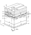
- FIG. 1 is a perspective cross-sectional view of an inversion type MOSFET having a trench gate structure according to a first embodiment
- FIG. 2A is a cross-sectional view of the MOSFET taken along the line IIA-IIA of FIG. 1
- FIG. 2B is a cross-sectional view taken along the line IIB-IIB of FIG. 1
- FIG. 2C is a cross-sectional view taken along the line IIC-IIC of FIG. 1
- FIG. 2D is a cross-sectional view taken along the line IID-IID of FIG. 1
- FIG. 1 is a perspective cross-sectional view of an inversion type MOSFET having a trench gate structure according to a first embodiment
- FIG. 2A is a cross-sectional view of the MOSFET taken along the line IIA-IIA of FIG. 1
- FIG. 2B is a cross-sectional view taken along the line IIB-IIB of FIG. 1
- FIG. 2C is a cross-section
- FIG. 3 is a partial perspective cross-sectional view of the vicinity of a trench shown while omitting therefrom a gate oxide film, a gate electrode, and the like in a trench gate structure;
- FIG. 4A is a cross-sectional view of the MOSFET taken along line IIB-IIB in FIG. 1 showing a manufacturing step of the MOSFET having a trench gate structure shown in FIG. 1;
- FIG. 4B is a cross-sectional view of the MOSFET taken along line IID-IID in FIG. 1 showing a manufacturing step of the MOSFET having a trench gate structure shown in FIG. 1;
- FIG. 4C is a cross-sectional view of the MOSFET taken along line IIB-IIB in FIG.
- FIG. 4D is a cross-sectional view of the MOSFET taken along line IID-IID in FIG. 1 showing a manufacturing step of the MOSFET having a trench gate structure shown in FIG. 1
- FIG. 4E is a cross-sectional view of the MOSFET taken along line IIB-IIB in FIG. 1 showing a manufacturing step of the MOSFET having a trench gate structure shown in FIG. 1
- FIG. 4F is a cross-sectional view of the MOSFET taken along line IID-IID in FIG. 1 showing a manufacturing step of the MOSFET having a trench gate structure shown in FIG. 1;
- FIG. 4D is a cross-sectional view of the MOSFET taken along line IID-IID in FIG. 1 showing a manufacturing step of the MOSFET having a trench gate structure shown in FIG. 1
- FIG. 4E is a cross-sectional view of the MOSFET taken along line IIB-IIB in FIG. 1 showing a manufacturing step of the MOSFET having a trench
- FIG. 5A is a cross-sectional view of the MOSFET taken along line IIB-IIB in FIG. 1 showing a manufacturing step of the MOSFET having a trench gate structure following those of FIGS. 4A, 4C and 4E;
- FIG. 5B is a cross-sectional view of the MOSFET taken along line IID-IID in FIG. 1 showing a manufacturing step of the MOSFET having a trench gate structure following those of FIGS. 4B, 4D and 4F;
- FIG. 5C is a cross-sectional view of the MOSFET taken along line IIB-IIB in FIG. 1 showing a manufacturing step of the MOSFET having a trench gate structure following those of FIGS. 4A, 4C and 4E;
- FIG. 5D is a cross-sectional view of the MOSFET taken along line IID-IID in FIG. 1 showing a manufacturing step of the MOSFET having a trench gate structure following those of FIGS. 4B, 4D and 4F;
- FIG. 5E is a cross-sectional view of the MOSFET taken along line IIB-IIB in FIG. 1 showing a manufacturing step of the MOSFET having a trench gate structure following those of FIGS. 4A, 4C and 4E;
- FIG. 5F is a cross-sectional view of the MOSFET taken along line IID-IID in FIG. 1 showing a manufacturing step of the MOSFET having a trench gate structure following those of FIGS. 4B, 4D and 4F;
- FIG. 5E is a cross-sectional view of the MOSFET taken along line IIB-IIB in FIG. 1 showing a manufacturing step of the MOSFET having a trench gate structure following those of FIGS. 4A, 4C and 4E;
- FIG. 5F
- FIG. 6 is a perspective cross-sectional view of a SiC semiconductor device according to a second embodiment
- FIG. 7A is a cross-sectional view taken along the line VIIA-VIIA in parallel with the xz plane in FIG. 6
- FIG. 7B is a cross-sectional view taken along the line VIIB-VIIB in parallel with the yz plane in FIG. 6
- FIG. 8 is a perspective cross-sectional view of a SiC semiconductor device according to a third embodiment
- FIG. 9A is a cross-sectional view taken along the line IXA-IXA in parallel with the xz plane in FIG. 8
- FIG. 9B is a cross-sectional view taken along the line IXB-IXB in parallel with the yz plane in FIG.
- FIG. 10A is a cross-sectional view of the MOSFET taken along line IXA-IXA in FIG. 8 showing a manufacturing step of the MOSFET having a trench gate structure shown in FIG. 8
- FIG. 10B is a cross-sectional view of the MOSFET taken along line IXB-IXB in FIG. 8 showing a manufacturing step of the MOSFET having a trench gate structure shown in FIG. 8
- FIG. 10C is a cross-sectional view of the MOSFET taken along line IXA-IXA in FIG. 8 showing a manufacturing step of the MOSFET having a trench gate structure shown in FIG. 8
- FIG. 10D is a cross-sectional view of the MOSFET taken along line IXB-IXB in FIG.
- FIG. 8 showing a manufacturing step of the MOSFET having a trench gate structure shown in FIG. 8
- FIG. 10E is a cross-sectional views of the MOSFET taken along line IXA-IXA in FIG. 8 showing a manufacturing step of the MOSFET having a trench gate structure shown in FIG. 8
- FIG. 10F is a cross-sectional view of the MOSFET taken along line IXB-IXB in FIG. 8 showing a manufacturing step of the MOSFET having a trench gate structure shown in FIG. 8
- FIG. 11A is a cross-sectional view of the MOSFET taken along line IXA-IXA in FIG. 8 showing a manufacturing step of the MOSFET having a trench gate structure following those of FIGS.
- FIG. 11B is a cross-sectional view of the MOSFET taken along line IXB-IXB in FIG. 8 showing a manufacturing step of the MOSFET having a trench gate structure following those of FIGS. 10B, 10D and 10F
- FIG. 11C is a cross-sectional view of the MOSFET taken along line IXA-IXA in FIG. 8 showing a manufacturing step of the MOSFET having a trench gate structure following those of FIGS. 10A, 10C and 10E
- FIG. 11D is a cross-sectional view of the MOSFET taken along line IXB-IXB in FIG. 8 showing a manufacturing step of the MOSFET having a trench gate structure following those of FIGS.
- FIG. 11E is a cross-sectional view of the MOSFET taken along line IXA-IXA in FIG. 8 showing a manufacturing step of the MOSFET having a trench gate structure following those of FIGS. 10A, 10C and 10E
- FIG. 11F is a cross-sectional view of the MOSFET taken along line IXB-IXB in FIG. 8 showing a manufacturing step of the MOSFET having a trench gate structure following those of FIGS. 10B, 10D and 10F
- FIG. 12 is a perspective cross-sectional view of a SiC semiconductor device according to a fourth embodiment
- FIG. 13A is a cross-sectional view taken along the line XIIIA-XIIIA in parallel with the xz plane in FIG. 12;
- FIG. 13B is a cross-sectional view taken along the line XIIIB-XIIIB in parallel with the yz plane in FIG. 12;
- FIG. 14 is a perspective cross-sectional view of a SiC semiconductor device according to a fifth embodiment;
- FIG. 15A is a cross-sectional view taken along the line XVA-XVA in parallel with the xz plane in FIG. 14;
- FIG. 15B is a cross-sectional view taken along the line XVB-XVB in parallel with the yz plane in FIG. 14.
- a first embodiment will next be described.
- an inversion type MOSFET with a trench gate structure will be described as an element equipped in a SiC semiconductor device.
- FIG. 1 is a perspective cross-sectional view of a MOSFET having a trench gate structure according to the present embodiment. This drawing corresponds to one cell of the MOSFET. Although only one cell of the MOSFET is shown in this diagram, two or more columns of MOSFETs having a similar structure to that of the MOSFET of FIG. 1 are arranged adjacent to each other.
- FIGS. 2A to 2D are cross-sectional views of the MOSFET of FIG. 1.
- FIG. 2A is a cross-sectional view taken along the line IIA-IIA in parallel with the xz plane in FIG. 1;
- FIG. 2B is a cross-sectional view taken along the line IIB-IIB in parallel with the xz plane in FIG. 1, FIG.
- FIG. 2C is a cross-sectional view of FIG. 1 taken along the line IIC-IIC in parallel with the yz plane in FIG. 1
- FIG. 2D is a cross-sectional view taken along the line IID-IID in parallel with the yz plane in FIG. 1.
- an n + type substrate 1 made of SiC is used as a semiconductor substrate.
- the n + type substrate 1 has, for example, a concentration of n type impurities, such as phosphorus, of 1.0x10 19 /cm 3 and a thickness of about 300 micrometer.
- This n + type substrate 1 has, on the surface thereof, an n - type drift layer 2 having, for example, a concentration of n type impurities, such as phosphorus, of from 3.0x10 15 /cm 3 to 7.0x10 15 /cm 3 and a thickness of from about 10 to 15 micrometer and made of SiC .
- the impurity concentration of this n - type drift layer 2 may be uniform in the depth direction, but preferably has a gradient concentration distribution in which the concentration of a portion of the n - type drift layer 2 on the side of the n + type substrate 1 is higher than that of a portion of the n - type drift layer 2 on the side distant from the n + type substrate 1.
- This n - type drift layer 2 has, in the surface layer portion thereof, a p type base region 3 and the p type base region 3 has thereover an n + type source region 4 and a p + type contact layer 5.
- the p type base region 3 has, for example, a concentration of p type impurities, such as boron or aluminum, of 5.0x10 16 to 2.0x10 19 /cm 3 and a thickness of about 2.0 micrometer.
- the n + type source region 4 has, in the surface layer thereof, for example, a concentration of n type impurities (surface concentration) such as phosphorus of 1.0x10 21 /cm 3 and a thickness of about 0.3 micrometer.
- the p + type contact layer 5 has, in the surface layer thereof, for example, a concentration of p type impurities (surface concentration) such as boron or aluminum of 1.0x10 21 /cm 3 and a thickness of about 0.3 micrometer.
- the n + type source region 4 is placed on both sides of a trench gate structure which will be described later and the p + type contact layer 5 is provided on the side opposite to the trench gate structure with the n + type source region 4 therebetween.
- a trench having, for example, a width of from 1.4 to 2.0 micrometer and a depth of 2.0 micrometer or greater (for example, 2.4 micrometer) is formed so as to penetrate through the p type base region 3 and the n + type source region 4 and reach the n - type drift layer 2.
- the p type base region 3 and the n + type source region 4 are placed so as to be in contact with the side surface of this trench 6.
- the inner wall surface of the trench 6 is covered with a gate oxide film 8 and the trench 6 is filled with a gate electrode 9 comprised of doped Poly-Si formed on the surface of the gate oxide film 8.
- the gate oxide film 8 is formed by thermally oxidizing the inner wall surface of the trench 6.
- the gate oxide film 8 has a thickness of about 100 nm both on the side surface and the bottom of the trench 6.
- the trench gate structure has such a constitution.
- This trench gate structure extends with the y direction in FIG. 1 as a longitudinal direction.
- Two or more trench gate structures are arranged in parallel along the x direction of FIG. 1, thus forming a stripe pattern.
- the n + type source region 4 and the p + type contact layer 5 also extend along the longitudinal direction of the trench gate structure.
- p type deep layers 10 extending in a direction crossing the trench gate structure are formed in the n - type drift layer 2 below the p type base region 3.
- the p type deep layers 10 extend in a normal direction (x direction in FIG. 1) relative to a portion of the side surface of the trench 6 in which a channel region is formed in the trench gate structure, that is, extend in a direction perpendicular to the longitudinal direction of the trench 6.
- a plurality of such p type deep layers 10 is arranged in the longitudinal direction of the trench 6.
- These p type deep layers 10 are formed deeper than the bottom of the trench 6.
- n - type drift layer 2 has a depth from about 2.6 to 3.0 micrometer (depth from the bottom portion of the p type base region 3 is, for example, from 0.6 to 1.0 micrometer).
- the p type deep layers 10 are in contact with the p type base region 3 so that they are fixed to a potential equal to that of the p type base region 3.
- FIG. 3 is a partial perspective cross-sectional view of the vicinity of the trench 6 shown while omitting therefrom the gate oxide film 8, the gate electrode 9, and the like in the trench gate structure.
- the p type deep layers 10 of the present embodiment are each equipped with a lower layer region 10a corresponding to the first region and an upper layer region 10b corresponding to the second region, which regions have widths varied in stepwise manner. This means that in the present embodiment, the width of each of the p type deep layers 10 differs in width in the depth direction and the width in the upper portion is smaller than that in the lower portion.
- the width of the lower layer region 10a is set greater in expectation of breakdown voltage, while in order to increase the width of a JFET region and thereby reduce a JFET resistance, the width of the upper layer region 10b is set smaller than in the lower layer region 10a.
- the concentration of p type impurities such as boron or aluminum is set at, for example, from 1.0x10 17 /cm 3 to 1.0x10 19 /cm 3 in expectation of breakdown voltage so as to mitigate the electric field concentration in the gate oxide film 8 and prevent dielectric breakdown.
- the depth of a boundary between the lower layer region 10a and the upper layer region 10b in other words, the depth of the bottom surface of the upper layer region 10b is deeper than the trench 6 and the upper layer region 10b extends from the side surface to the bottom portion of the trench 6.
- the width of the channel becomes a portion of the n - drift layer 2 between narrow-width upper layer regions 10b up to the deepest portion of the trench 6 so that it becomes wider than the portion located between the lower layer regions 10a.
- the width of a JFET region can be made wider compared with the case where all the widths of each of the p type deep layers 10 are made equal to that of the lower layer region 10a, making it possible to reduce a JFET resistance.
- the n + type source region 4, the p + type contact layer 5, and the gate electrode 9 have on the surfaces thereof a source electrode 11 and gate wiring (not illustrated).
- the source electrode 11 and the gate wiring are each comprised of a plurality of metals (for example, Ni/Al).
- n type SiC (more specifically, the n + type source region 4 and, when doped with n, the gate electrode 9) is comprised of a metal which can form an ohmic contact with the n type SiC and at least a portion of them to be brought into contact with a p type SiC (more specifically, p + type contact layer 5 and, when doped with p, the gate electrode 9) is comprised of a metal which can form an ohmic contact with the p type SiC.
- the source electrode 11 and the gate wiring are formed on an interlayer insulating film 12 and therefore they are electrically insulated. Through a contact hole formed in the interlayer insulating film 12, the source electrode 11 is brought into electric contact with the n + type source region 4 and the p + type contact layer 5 and the gate wiring is brought into electric contact with the gate electrode 9.
- the n + type substrate 1 has, on the back surface side thereof, a drain electrode 13 electrically coupled to the n + type substrate 1.
- Such a structure constitutes an n channel and inversion type MOSFET having a trench gate structure.
- Such an inversion type MOSFET having a trench gate structure operates as follows. Before a gate voltage is applied to the gate electrode 9, no inversion layer is formed in the p type base region 3. Accordingly, even if a positive voltage is applied to the drain electrode 13, electrons cannot reach the p type base region 3 from the n + type source region 4 and no electric current flows between the source electrode 11 and the drain electrode 13.
- the depletion layer expands about 0.7 micrometer toward the p type base region 3 and about 7.0 micrometer toward the n - type drift layer 2.
- the thickness of the p type base region 3 is set to 2.0 micrometer that is thicker than the expanding amount of the depletion layer so that occurrence of punching through can be prevented. Then, because the depletion layer expands more than the case where the drain is 0 V and a region that acts as an insulator further expands, electric current does not flow between the source electrode 11 and the drain electrode 13.
- the gate voltage is 0 V
- an electric field is applied between the drain and the gate. Therefore, an electric field concentration may occur at the bottom of the gate oxide film 8.
- the p type deep layers 10 deeper than the trench 6 are provided, however, the depletion layer at a PN junction between the p type deep layers 10 and the n - type drift layer 2 largely expands toward the n - type drift layer 2 and a high voltage due to the influence of the drain voltage does not easily go into the gate oxide film 8.
- the width of the lower layer region 10a of the p type deep layers 10 is preset in expectation of a breakdown voltage so that it is possible to prevent a higher voltage from going into the gate oxide film 8.
- an electric field concentration in the gate oxide film 8 especially, an electric field concentration in the gate oxide film 8 at the bottom of the trench 6 can be mitigated, whereby breakage of the gate oxide film 8 can be prevented.
- a gate voltage of 20V is applied to the gate electrode 9 so that a channel is formed on the surface of the p type base region 3 which is in contact with the trench 6. Electrons injected from the source electrode 11 reach the n - type drift layer 2 after passing through the n + type source region 4 and the channel formed on the p type base region 3. Accordingly, electric current can be provided between the source electrode 11 and the drain electrode 13.
- the width of the upper layer region 10b of the p type deep layers 10 is made narrower than that of the lower layer region 10a and the width decreases in stepwise manner with a decrease in the depth of the p type deep layers 10.
- the channel can have a greater width.
- the width of a channel corresponds to a portion of the n - type drift layer 2 located between two small-width upper layer regions 10b so that it becomes wider than a portion of the n - type drift layer 2 located between wide-width lower layer portions 10a.
- the channel gets wider width.
- the width of the JFET region can be made wider, making it possible to reduce the JFET resistance.
- FIGS. 4A to 4F and 5A to 5F are cross-sectional views showing manufacturing steps of the MOSFET having a trench gate structure as shown in FIG. 1.
- a cross-sectional view (area corresponding to FIG. 2B) taken along the line IIB-IIB in parallel with the xz plane in FIG. 1 is shown on the left side
- a cross-sectional view (area corresponding to FIG. 2D) taken along the line IID-IID in parallel with the yz plane in FIG. 1 is shown on the right side.
- the description will next be made referring to these drawings.
- an n + type substrate 1 having, for example, a concentration of n type impurities, such as phosphorous, of 1.0x10 19 /cm 3 and a thickness of about 300 micrometer is prepared.
- an n - type drift layer 2 having, for example, a concentration of n type impurities, such as phosphorus, of from 3.0x10 15 /cm 3 to 7.0x10 15 /cm 3 and a thickness of about 15 micrometer and made of SiC is formed by epitaxial growth.
- Step shown in FIGS. 4C and 4D After formation of a mask 20 made of LTO or the like on the surface of the n - type drift layer 2, the mask 20 is opened at a predetermined formation region of a lower layer region 10a of p type deep layers 10 through photolithography. Then, p type impurities (such as boron or aluminum) are implanted from above the mask 20. Ion implantation is performed to give a boron or aluminum concentration of, for example, from 1.0x10 17 /cm 3 to 1.0x10 19 /cm 3 . Then, the mask 20 is removed.
- p type impurities such as boron or aluminum
- Step shown in FIGS. 4E and 4F After formation of a mask 21 made of LTO or the like on the surface of the n - type drift layer 2, the mask 21 is opened at a predetermined formation region of an upper layer region 10b of the p type deep layers 10 through photolithography. Then, p type impurities (such as boron or aluminum) are implanted from above the mask 21. The concentration upon ion implantation is set similar to that in the step shown in FIGS. 4C and 4D. After removal of the mask 21, the ions thus implanted are activated.
- p type impurities such as boron or aluminum
- ion implantation of p type impurities for the formation of the lower layer region 10a is followed by ion implantation of p type impurities for the formation of the upper layer region 10b, but they may be performed in reverse order.
- ion implantation of p type impurities for the formation of the upper layer region 10b is performed first, it is also possible to use the mask 21 in common to form the lower layer region 10a.
- the opening end of the opening portion formed in the mask 21 is caused to retreat by etching with hydrofluoric acid or the like and the width of the opening portion is changed to a width corresponding to the lower layer region 10a.
- the mask 21 changed in the width of the opening portion, p type impurities are implanted in order to form the lower layer region 10a.
- This permits using a mask in common.
- the opening end of the mask 21 to retreat by etching and thereby forming an opening portion corresponding to the lower layer region 10a, the upper layer region 10a and the lower layer region 10b can be formed in self alignment, making it possible to avoid an influence of misalignment.
- a p type base region 3 is formed by the epitaxial growth of a p type impurity layer having, for example, a concentration of p type impurities, such as boron or aluminum, of from 5.0x10 15 to 5.0x10 16 /cm 3 and a thickness of about 2.0 micrometer on the surface of the n - type drift layer 2.
- a concentration of p type impurities such as boron or aluminum
- Step shown in FIGS. 5C and 5D Then, after formation of a mask (not illustrated) made of, for example, LTO on the p type base region 3, photolithography is conducted to form an opening in the mask at a predetermined formation region of an n + type source region 4. After that, n type impurities (such as nitrogen) are implanted.
- n + type source region 4 having, for example, a concentration (surface concentration) of n type impurities such as phosphorus of 1.0x10 21 /cm 3 and a thickness of about 0.3 micrometer
- p + type contact layer 5 having, for example, a concentration (surface concentration) of p type impurities such as boron or aluminum of about 1.0x10 21 /cm 3 and a thickness of about 0.3 micrometer.
- Step shown in FIGS. 5E and 5F After formation of an etching mask, which is not illustrated, on the p type base region 3, the n + type source region 4, and the p + type contact layer 5, the etching mask is opened at a predetermined formation region of a trench 6. Then, anisotropic etching is performed with the etching mask, followed by isotropic etching or sacrificial oxidation if needed to form the trench 6. After this, the etching mask is removed.
- Steps thereafter are similar to the conventional steps so that they are not illustrated.
- a gate oxide film formation step is performed to form a gate oxide film 8 on the entire surface of the substrate including the inside of the trench 6. More specifically, the gate oxide film 8 is formed by gate oxidation (thermal oxidation) by a pyrogenic method using a wet atmosphere.
- gate oxidation thermal oxidation
- an about 440-nm thick polysilicon layer doped with n type impurities is formed on the surface of the gate oxide film 8 at a temperature of, for example, 600 degrees C and then, an etch back step or the like is performed to make the poly silicon layer thinner.
- the interlayer insulating film 12 is patterned to form contact holes to be connected to the n + type source region 4 or the p + type contact layer 5 and at the same time, to form contact holes to be connected to the gate electrode 9 on another cross section.
- a film of an electrode material is formed to fill the contact holes therewith, it is patterned to form a source electrode 11 and a gate wiring.
- a drain electrode 13 is formed on the back surface side of the n + type substrate 1. As a result, the MOSFET shown in FIG. 1 is completed.
- the SiC semiconductor device of the present embodiment has a structure in which the width of the p type deep layers 10 is made smaller in stepwise manner with a decrease in the depth thereof.
- the p type deep layers 10 are each comprised of a lower layer region 10a and an upper layer region 10b and the width of the upper layer region 10b is made smaller than that of the lower layer region 10a.
- this structure leads to an increase in the width of the channel near the upper portion of the p type deep layers 10, an increase in the width of a JFET region compared with the case where the width of each of the p type deep layers 10 is made uniform in any portion, that is, the whole width is made equal to the width of the lower layer region 10a, and a reduction in JFET resistance.
- the p type deep layers 10 are formed so as to cross the trench 6 constituting the trench gate structure, the JFET resistance in the JFET region formed between two p type deep layers 10 adjacent to each other can be reduced, making it possible to reduce the on resistance.
- SiC semiconductor device of this embodiment is different from that of the first embodiment in the structure of the p type deep layers 10. Since they are similar in the fundamental structure, only portions different from the first embodiment will next be described.
- FIG. 6 is a perspective cross-sectional view of the SiC semiconductor device according to this embodiment.
- FIG. 7A is a cross-sectional view taken along the line VIIA-VIIA in parallel with the xz plane in FIG. 6 and
- FIG. 7B is a cross-sectional view taken along the line VIIB-VIIB in parallel with the yz plane in FIG. 6.
- the width of each of the p type deep layers 10 is changed in the depth direction of the p type deep layers 10 and the width of the upper portion of the p type deep layers 10 is made smaller than that of the lower portion. More specifically, the width of the bottom portion of the p type deep layers 10 is set in consideration of a breakdown voltage and from the bottom portion thereof, the width is decreased gradually with a decrease in the depth of the p type deep layers 10.
- the width of the bottom portion of the p type deep layers 10 is made wider to ensure a breakdown voltage and at the same time, a wide channel can be formed by decreasing the width of the upper portion of the p type deep layers 10. This enables widening of a current path. As a result, a JFET resistance in a JFET region formed between two adjacent p type deep layers 10 can be reduced further and a further reduction in on resistance can be achieved.
- the manufacturing method of a SiC semiconductor device having the structure of the present embodiment is basically similar to that of the first embodiment. It is only necessary to diagonally implant p type impurities with the mask 21 when the p type deep layers 10 as shown in FIG. 4C and 4D are formed, and thereby form the p type deep layers 10 in the diagonal direction.
- the SiC semiconductor device of this embodiment has a structure capable of reducing the on resistance further compared with that of the first embodiment. Since they are similar in the fundamental structure, only portions different from the first embodiment will next be described.
- FIG. 8 is a perspective cross-sectional view of the SiC semiconductor device according to the present embodiment.
- FIG. 9A is a cross-sectional view taken along the line IXA-IXA in parallel with the xz plane in FIG. 8 and
- FIG. 9B is a cross-sectional view taken along the line IXB-IXB in parallel with the yz plane in FIG. 8.
- a current diffusion layer 2a is formed by setting high the n type impurity concentration on the surface side of the n - type drift layer 2, that is, on the side opposite to the n + type substrate 1.
- the current diffusion layer 2a is provided in order to widen a current flowing region in an on state and the current diffusion layer 2a has an impurity concentration of, for example, from 5.0x10 16 to 1.5x10 17 /cm 3 .
- the current diffusion layer 2a has, for example, a thickness of from 0.3 to 0.7 micrometer. In the present embodiment, it is equal to the depth of the upper layer region 10b of the p type deep layers 10.
- the SiC semiconductor device having such a structure, when a gate voltage is applied to the gate electrode 9 in an on state, a channel is formed on the surface of the p type base region 3 contiguous to the trench 6 and electrons injected from the source electrode 11 reach the current diffusion layer 2a of the n - type drift layer 2 after passing through the n + type source region 4 and the channel formed on the p type base region 3.
- a current flowing region becomes wider in the low-resistance current diffusion layer 2a and electric current reaches even a position distant from the trench gate structure, which contributes to a further reduction in on-resistance.
- the p type deep layers 10 each comprised of the lower layer region 10a and the upper layer region 10b may be equipped with the current diffusion layer 2a. This enables to achieve a further reduction in on-resistance.
- FIGS. 10A to 10F and FIGS. 11A to 11F are cross-sectional views showing manufacturing steps of such a SiC semiconductor device of the present embodiment.
- a cross-sectional view (area corresponding to FIG. 9A) taken along the line IXA-IXA in parallel with the xz plane in FIG. 8 is shown on the left side and a cross-sectional view (area corresponding to FIG. 9B) taken along the line IXB-IXB in parallel with the yz plane in FIG. 8 is shown on the right side.
- the manufacturing method of the SiC semiconductor device of the present embodiment will next be described referring to these drawings.
- an n - type drift layer 2 is formed by epitaxial growth on the surface of the n + type semiconductor substrate 1. At this time, a portion of the n - type drift layer 2 other than the current diffusion layer 2a is formed (first step). Then, in the step shown in FIG. 10C and 10D, after a mask 20 is placed on the surface of the n - type drift layer 2, the mask 20 is opened at a predetermined formation region of an upper layer region 10b of p type deep layers 10. P type impurities (such as boron or aluminum) are implanted from above the mask 20.
- P type impurities such as boron or aluminum
- a current diffusion layer 2a having, for example, an n type impurity concentration of from 5.0x10 16 to 1.5x10 17 /cm 3 and a thickness of from 0.3 to 0.7 micrometer is formed (second step).
- the mask 21 is opened at a predetermined formation region of an upper layer region 10b of the p type deep layers 10.
- p type impurities such as boron or aluminum
- the ions thus implanted are activated.
- the upper layer region 10 b is formed by partial p-type compensation of the current diffusion layer 2a and is then connected to the lower layer region 10a formed in advance to constitute the p type deep layers 10.
- steps similar to those employed in those shown in FIGS. 5A to 5F are performed to complete the SiC semiconductor device of the present embodiment shown in FIG. 8.
- the SiC semiconductor device of the present embodiment has a structure more effective than that of the third embodiment in mitigating a field effect concentration in the gate oxide film 8. It is basically similar to the third embodiment so that only a portion different from the third embodiment will next be described.
- FIG. 12 is a perspective cross-sectional view of the SiC semiconductor device according to the present embodiment.
- FIG. 13A is a cross-sectional view taken along the line XIIIA-XIIIA in parallel with the xz plane in FIG. 12 and
- FIG. 13B is a cross-sectional view taken along the line XIIIB-XIIIB in parallel with the yz plane in FIG. 12.
- the current diffusion layer 2a is formed on the surface side of the n - type drift layer 2 as in the third embodiment and at the same time, the trench 6 penetrates through the current diffusion layer 2a and the bottom of the trench 6 is formed at a position deeper than the current diffusion layer 2a.
- the electric field concentration to the gate oxide film 8 can be mitigated more than that in the third embodiment.
- the current diffusion layer 2a is a portion of the n - type drift layer 2 having a relatively high impurity concentration and an electric field concentration tends to occur at a site where the impurity concentration is high.
- the electric field concentration can be mitigated by extending the depth of the trench gate structure to a position deeper than the current diffusion layer 2a, that is, a position having a relatively low impurity concentration in the n - type drift layer 2. As a result, it becomes possible to prevent the gate oxide film 8 from being broken by the electric field concentration.
- the manufacturing method of the SiC semiconductor device having such a structure is almost similar to that of the third embodiment. It is only necessary to change the formation depth of the trench 6 in the step of FIG. 1E and 11F described in the third embodiment and extend the depth of the trench 6 to exceed the current diffusion layer 2a. Needless to say, it is also possible not to change the formation depth of the trench 6 but to decrease the thickness of the current diffusion layer 2a compared with that of the third embodiment, thereby extending the bottom of the trench 6 to a position deeper than the current diffusion layer 2a.
- the SiC semiconductor device of the present embodiment is different from that of the third embodiment in the concentration of the current diffusion layer 2a. It is similar to the third embodiment in basic structure so that only a portion different from that of the third embodiment will next be described.
- FIG. 14 is a perspective cross-sectional view of the SiC semiconductor device of the present embodiment.
- FIGS. 15A is a cross-sectional view taken along the line XVA-XVA in parallel with the xz plane in FIG. 14 and
- FIG. 15B is a cross-sectional view taken along the line XVB-XVB in parallel with the yz plane in FIG. 14, respectively.
- the current diffusion layer 2a is formed on the surface side of the n - type drift layer 2 as in the third embodiment.
- a concentration distribution is provided in the current diffusion layer 2a so that the n type impurity concentration of the current diffusion layer 2a is lower in the lower portion and higher in the upper portion.
- the concentration of n type impurities in the lower portion of the current diffusion layer 2a is set lower so that the bottom portion of the trench 6 is located at a position having a relatively low impurity concentration. This enables to mitigate the electric field concentration to the gate oxide film 8.
- the n type impurity concentration is made higher in the upper portion of the current diffusion layer 2a so that a current flowing region can be widened further in the low-resistance current diffusion layer 2a and a reduction in on resistance can also can be achieved. Accordingly, both the prevention of breakage of the gate oxide film 8 due to a high electric field and the reduction in on resistance can be achieved.
- a manufacturing method of the SiC semiconductor device having such a structure is almost similar to that of the third embodiment. It is only necessary to perform epitaxial growth for the formation of the current diffusion layer 2a in the step of FIG. 10E and 10F described in the third embodiment while gradually increasing the doping amount of n type impurities.
- Such a structure in which the current diffusion layer 2a has, in the depth direction thereof, a distribution in the n type impurity concentration can also be applied to the fourth embodiment described above.
- the p type deep layers 10 have a width showing a stepwise decrease with a decrease in the depth of the p type deep layers and in the second embodiment, the p type deep layers 10 have a width showing a gradual decrease width with a decrease in the depth of the p type deep layers 10.
- the p type deep layers 10 have a width narrower in the upper portion and wider in the lower portion.
- the number of steps may be increased to more than two.
- the p type deep layers 10 are extended in the x direction, but the p type deep layers 10 may be diagonally crossed with the longitudinal direction of the trench 6 or may be divided into two or more layers in the x direction. In the case where the p type deep layers 10 are diagonally crossed with the longitudinal direction of the trench 6, it is preferred, in order to prevent an uneven equipotential distribution, to arrange the p type deep layers 10 in line symmetry, with a line extending in a direction perpendicular to the longitudinal direction of the trench 6 as a symmetry line.
- the description is made with, as an example, an n channel type MOSFET having an n type as the first conductivity type and a p type as the second conductivity type.
- the disclosure can also be applied to a p channel type MOSFET in which the conductivity type of each of the constituting elements have been reversed.
- a MOSFET having a trench gate structure is used as an example.
- the disclosure can also be applied to an IGBT having a similar trench gate structure.
- the structure or the manufacturing method of the IGBT is similar to that of the above embodiments except that the conductivity type of the substrate 1 is changed from n type to p type.
- the gate oxide film 8 made by thermal oxidation is used as an example of a gate insulating film.
- the gate insulating film is not limited thereto but it may include an oxide film not formed by thermal oxidation or a nitride film.
- the manufacturing method of a SiC semiconductor device includes steps shown in FIGS. 10A to 10F and FIGS. 11A to 11F.
- the SiC semiconductor device having the structure shown in FIG. 8 can be manufactured.
- the current diffusion layer 2a is formed in the structure in which each of the p type deep layers 10 is comprised of the lower layer region 10a and the upper layer region 10b as in the first embodiment, but it is also possible to form the current diffusion layer 2a in the structure of the second embodiment.
- a silicon carbide semiconductor device includes: an inversion type semiconductor switching element.
- the inversion type semiconductor switching element includes: a substrate having a first or second conductivity type and made of silicon carbide; a drift layer disposed on the substrate, having an impurity concentration lower than the substrate, having the first conductivity type, and made of silicon carbide; a base region disposed on the drift layer, having the second conductivity type, and made of silicon carbide; a source region disposed in an upper portion of the base region, having an impurity concentration higher than the drift layer, having the first conductivity type, and made of silicon carbide; a contact region disposed in another upper portion of the base region, having an impurity concentration higher than the base layer, having the second conductivity type, and made of silicon carbide; a trench extending from a surface of the source region to penetrate the base region and having a first direction as a longitudinal direction; a gate insulating film disposed on an inner wall of the trench; a gate electrode disposed on the gate
- the inversion type semiconductor switching element is configured to flow current between the source electrode and the drain electrode via the source region, an inversion type channel region and the drift layer.
- the inversion type channel region is provided in a portion of the base region positioned on a side of the trench by controlling a voltage applied to the gate electrode.
- the inversion type semiconductor switching element further includes: a plurality of deep layers having the second conductivity type. Each deep layer is disposed in an upper portion of the drift layer below the base region, has a depth deeper than the trench, and extends along a second direction, which crosses the first direction. Each deep layer has an upper portion and a lower portion. A width of the upper portion is narrower than the lower portion.
- a channel width around the upper portion of the deep layer is expanded when a gate voltage is applied to the gate electrode to form the channel around the upper portion of the deep layer.
- a width of a JFET region is wider than a case where a width of the deep layer is constant. In this case, a JFET resistance is reduced, and an on-state resistance is also reduced.
- a width of each deep layer may decrease in a stepwise manner as a depth of the deep layer gets shallower.
- a width of each deep layer may decrease gradually as a depth of the deep layer gets shallower.
- the inversion type semiconductor switching element may further include a current diffusion layer having the first conductivity type.
- the current diffusion layer is disposed in the drift layer between the plurality of deep layers, and the current diffusion layer has an impurity concentration higher than the drift layer, which is located below the deeper layer. Since the current diffusion layer has a low resistance, an area in the current diffusion layer, in which the current flows, is expanded, so that the on-state resistance is much reduced.
- a bottom of the trench may be deeper than the current diffusion layer.
- the trench reaches the drift layer, which has a comparatively low impurity concentration, so that an electric field concentration is reduced.
- the device protects the gate insulation film from being damaged by the electric field concentration.
- the current diffusion layer may have an impurity concentration distribution in a depth direction, and the impurity concentration of the current diffusion layer increases as a depth of the current diffusion layer gets shallower.
- the lower portion of the current diffusion layer has a comparatively low impurity concentration
- the bottom of the trench is disposed at the lower portion of the current diffusion layer having the low impurity concentration. Accordingly, the electric field concentration at the gate insulation film is reduced.
- the upper portion of the current diffusion layer has a comparatively high impurity concentration, an area in the current diffusion layer having the low resistance, in which the current flows, is expanded. Thus, the on-state resistance is reduced. In this case, the damage of the gate insulation film is prevented, and the on-state resistance is reduced.
- a method for manufacturing a silicon carbide semiconductor device includes: forming a drift layer on a substrate, wherein the substrate is made of silicon carbide and has a first or second conductivity type, and the drift layer is made of silicon carbide, has the first conductivity type, and has an impurity concentration lower than the substrate; forming a plurality of deep layers having the second conductivity type in a surface portion of the drift layer by implanting ions on a surface of the drift layer through a first mask after the first mask is formed on the surface of the drift layer; forming a base region having the second conductivity type and made of silicon carbide on the deep layers and the drift layer; forming a source region in a surface portion of the base region by implanting a first conductivity type impurity on a surface of the base region, wherein the source region has an impurity concentration higher than the drift layer, having the first conductivity type, and made of silicon carbide; forming a contact region in another surface portion of the base region by implanting
- Each deep layer is disposed in an upper portion of the drift layer below the base region, has a depth deeper than the trench, and extends along a second direction, which crosses the first direction.
- Each deep layer has an upper portion and a lower portion, and a width of the upper portion is narrower than the lower portion.
- a channel width around the upper portion of the deep layer is expanded when a gate voltage is applied to the gate electrode to form the channel around the upper portion of the deep layer.
- a width of a JFET region is wider than a case where a width of the deep layer is constant. In this case, a JFET resistance is reduced, and an on-state resistance is also reduced.
- the forming of the deep layers may include: forming a second mask on the surface of the drift layer; partially opening the second mask; implanting a second conductivity type impurity on the surface of the drift layer through the second mask to form a first region of each deep layer; forming a third mask on the surface of the drift layer; partially opening the third mask; and implanting a second conductivity type impurity on the surface of the drift layer through the third mask to form a second region of each deep layer.
- the second region is located above the first region, and a width of the second region is narrower than the first region.
- the forming of the deep layers may include: forming a third mask on the surface of the drift layer; partially opening the third mask; implanting a second conductivity type impurity on the surface of the drift layer through the third mask to form a second region of each deep layer; expanding an opening of the third mask so that a second mask having an opening corresponding to a first region of each deep layer is formed; and implanting a second conductivity type impurity on the surface of the drift layer through the second mask to form the first region of each deep layer.
- the second region is located above the first region, and a width of the second region is narrower than the first region.
- the method for manufacturing the silicon carbide semiconductor device may further include: forming a current diffusion layer having the first conductivity type in the drift layer between the plurality of deep layers.
- the current diffusion layer has an impurity concentration higher than the drift layer, which is located below the deeper layer.
- the implanting of the second conductivity type impurity to form the first region of each deep layer is performed after the forming of the drift layer and before the forming of the current diffusion layer so that the first region of each deep layer is embedded in the drift layer, and the implanting of the second conductivity type impurity to form the second region of each deep layer is performed after the forming of the current diffusion layer so that the second region of each deep layer is embedded in the current diffusion layer.
Abstract
Description
First, an n+ type substrate 1 having, for example, a concentration of n type impurities, such as phosphorous, of 1.0x10¹⁹ /cm3 and a thickness of about 300 micrometer is prepared. On the surface of the n+ type substrate 1, an n-
After formation of a
After formation of a
A p
Then, after formation of a mask (not illustrated) made of, for example, LTO on the p
After formation of an etching mask, which is not illustrated, on the p
A second embodiment will next be described. The SiC semiconductor device of this embodiment is different from that of the first embodiment in the structure of the p type deep layers 10. Since they are similar in the fundamental structure, only portions different from the first embodiment will next be described.
A third embodiment will next be described. The SiC semiconductor device of this embodiment has a structure capable of reducing the on resistance further compared with that of the first embodiment. Since they are similar in the fundamental structure, only portions different from the first embodiment will next be described.
A fourth embodiment will next be described. The SiC semiconductor device of the present embodiment has a structure more effective than that of the third embodiment in mitigating a field effect concentration in the
A fifth embodiment will next be described. The SiC semiconductor device of the present embodiment is different from that of the third embodiment in the concentration of the
In each of the above embodiments, examples of the structure in which the p type
Claims (10)
- A silicon carbide semiconductor device comprising:
an inversion type semiconductor switching element,
wherein the inversion type semiconductor switching element includes:
a substrate (1) having a first or second conductivity type and made of silicon carbide;
a drift layer (2) disposed on the substrate (1), having an impurity concentration lower than the substrate (1), having the first conductivity type, and made of silicon carbide;
a base region (3) disposed on the drift layer (2), having the second conductivity type, and made of silicon carbide;
a source region (4) disposed in an upper portion of the base region (3), having an impurity concentration higher than the drift layer (2), having the first conductivity type, and made of silicon carbide;
a contact region (5) disposed in another upper portion of the base region (3), having an impurity concentration higher than the base layer (3), having the second conductivity type, and made of silicon carbide;
a trench (6) extending from a surface of the source region (4) to penetrate the base region (3) and having a first direction as a longitudinal direction;
a gate insulating film (8) disposed on an inner wall of the trench (6);
a gate electrode (9) disposed on the gate insulating film (8) in the trench (6);
a source electrode (11) electrically coupled with the source region (4) and the base region (3); and
a drain electrode (13) disposed on a back side of the substrate (1),
wherein the inversion type semiconductor switching element is configured to flow current between the source electrode (11) and the drain electrode (13) via the source region (4), an inversion type channel region and the drift layer (2),
wherein the inversion type channel region is provided in a portion of the base region (3) positioned on a side of the trench (6) by controlling a voltage applied to the gate electrode (9),
wherein the inversion type semiconductor switching element further includes: a plurality of deep layers (10) having the second conductivity type,
wherein each deep layer (10) is disposed in an upper portion of the drift layer (2) below the base region (3), has a depth deeper than the trench (6), and extends along a second direction, which crosses the first direction,
wherein each deep layer (10) has an upper portion (10b) and a lower portion (10a), and
wherein a width of the upper portion (10b) is narrower than the lower portion (10a). - The silicon carbide semiconductor device according to claim 1,
wherein a width of each deep layer (10) decreases in a stepwise manner as a depth of the deep layer (10) gets shallower. - The silicon carbide semiconductor device according to claim 1,
wherein a width of each deep layer (10) decreases gradually as a depth of the deep layer (10) gets shallower. - The silicon carbide semiconductor device according to any one of claims 1 to 3,
wherein the inversion type semiconductor switching element further includes a current diffusion layer (2a) having the first conductivity type,
wherein the current diffusion layer (2a) is disposed in the drift layer (2) between the plurality of deep layers, and
wherein the current diffusion layer (2a) has an impurity concentration higher than the drift layer (2), which is located below the deeper layer (10). - The silicon carbide semiconductor device according to claim 4,
wherein a bottom of the trench (6) is deeper than the current diffusion layer (2a). - The silicon carbide semiconductor device according to claim 4 or 5,
wherein the current diffusion layer (2a) has an impurity concentration distribution in a depth direction, and
wherein the impurity concentration of the current diffusion layer (2a) increases as a depth of the current diffusion layer (2a) is made shallow. - A method for manufacturing a silicon carbide semiconductor device comprising:
forming a drift layer (2) on a substrate (1), wherein the substrate (1) is made of silicon carbide and has a first or second conductivity type, and the drift layer (2) is made of silicon carbide, has the first conductivity type, and has an impurity concentration lower than the substrate (1);
forming a plurality of deep layers (10) having the second conductivity type in a surface portion of the drift layer (2) by implanting an ion on a surface of the drift layer (2) through a first mask after the first mask is formed on the surface of the drift layer (2);
forming a base region (3) having the second conductivity type and made of silicon carbide on the deep layers (10) and the drift layer (2);
forming a source region (4) in a surface portion of the base region (3) by implanting a first conductivity type impurity on a surface of the base region (3), wherein the source region (4) has an impurity concentration higher than the drift layer (2), having the first conductivity type, and made of silicon carbide;
forming a contact region (5) in another surface portion of the base region (3) by implanting a second conductivity type impurity on the surface of the base region (3), wherein the contact region (5) has an impurity concentration higher than the base region (3), having the second conductivity type, and made of silicon carbide;
forming a trench (6) on a surface of the source region (4) to penetrate the base region (3) and to reach the drift layer (2), wherein the trench (6) is shallower than each deep layer (10), and has a first direction as a longitudinal direction;
forming a gate insulating film (8) on an inner wall of the trench (6);
forming a gate electrode (9) on the gate insulating film (8) in the trench (6);
forming a source electrode (11) to be electrically coupled with the base region (3) via the source region (4) and the contact region (5); and
forming a drain electrode (13) on a back side of the substrate (1),
wherein each deep layer (10) is disposed in an upper portion of the drift layer (2) below the base region (3), has a depth deeper than the trench (6), and extends along a second direction, which crosses the first direction,
wherein each deep layer (10) has an upper portion (10b) and a lower portion (10a), and
wherein a width of the upper portion (10b) is smaller than the lower portion (10a). - The method for manufacturing the silicon carbide semiconductor device according to claim 7,
wherein the forming of the deep layers (10) includes:
forming a second mask (20) on the surface of the drift layer (2);
partially opening the second mask (20);
implanting a second conductivity type impurity on the surface of the drift layer (2) through the second mask (20) to form a first region (10a) of each deep layer (10);
forming a third mask (21) on the surface of the drift layer (2);
partially opening the third mask (21); and
implanting a second conductivity type impurity on the surface of the drift layer (2) through the third mask (21) to form a second region (10b) of each deep layer (10),
wherein the second region (10b) is located above the first region (10a), and
wherein a width of the second region (10b) is smaller than the first region (10a). - The method for manufacturing the silicon carbide semiconductor device according to claim 7,
wherein the forming of the deep layers (10) includes:
forming a third mask (21) on the surface of the drift layer (2);
partially opening the third mask (21);
implanting a second conductivity type impurity on the surface of the drift layer (2) through the third mask (21) to form a second region (10b) of each deep layer (10);
expanding an opening of the third mask (21) so that a second mask (20) having an opening corresponding to a first region (10a) of each deep layer (10) is formed; and
implanting a second conductivity type impurity on the surface of the drift layer (2) through the second mask (20) to form the first region (10a) of each deep layer (10),
wherein the second region (10b) is located above the first region (10a), and
wherein a width of the second region (10b) is smaller than the first region (10a). - The method for manufacturing the silicon carbide semiconductor device according to claim 8 further comprising:
forming a current diffusion layer (2a) having the first conductivity type in the drift layer (2) between the plurality of deep layers,
wherein the current diffusion layer (2a) has an impurity concentration higher than the drift layer (2), which is located below the deeper layer (10),
wherein the implanting of the second conductivity type impurity to form the first region (10a) of each deep layer (10) is performed after the forming of the drift layer (2) and before the forming of the current diffusion layer (2a) so that the first region (10a) of each deep layer (10) is embedded in the drift layer (2), and
wherein the implanting of the second conductivity type impurity to form the second region (10b) of each deep layer (10) is performed after the forming of the current diffusion layer (2a) so that the second region (10b) of each deep layer (10) is embedded in the current diffusion layer (2a).
Priority Applications (3)
| Application Number | Priority Date | Filing Date | Title |
|---|---|---|---|
| DE112012000748.4T DE112012000748T5 (en) | 2011-02-11 | 2012-02-06 | Silicon carbide semiconductor device and method of manufacturing the same |
| CN2012800083291A CN103348478A (en) | 2011-02-11 | 2012-02-06 | Silicon carbide semiconductor device and method for manufacturing the same |
| US13/994,855 US20140175459A1 (en) | 2011-02-11 | 2012-02-06 | Silicon carbide semiconductor device and method for manufacturing the same |
Applications Claiming Priority (2)
| Application Number | Priority Date | Filing Date | Title |
|---|---|---|---|
| JP2011027995A JP2012169384A (en) | 2011-02-11 | 2011-02-11 | Silicon carbide semiconductor device and method of manufacturing the same |
| JP2011-027995 | 2011-02-11 |
Publications (1)
| Publication Number | Publication Date |
|---|---|
| WO2012108166A1 true WO2012108166A1 (en) | 2012-08-16 |
Family
ID=45774298
Family Applications (1)
| Application Number | Title | Priority Date | Filing Date |
|---|---|---|---|
| PCT/JP2012/000769 WO2012108166A1 (en) | 2011-02-11 | 2012-02-06 | Silicon carbide semiconductor device and method for manufacturing the same |
Country Status (5)
| Country | Link |
|---|---|
| US (1) | US20140175459A1 (en) |
| JP (1) | JP2012169384A (en) |
| CN (1) | CN103348478A (en) |
| DE (1) | DE112012000748T5 (en) |
| WO (1) | WO2012108166A1 (en) |
Cited By (4)
| Publication number | Priority date | Publication date | Assignee | Title |
|---|---|---|---|---|
| CN104282758A (en) * | 2013-07-02 | 2015-01-14 | 通用电气公司 | Metal-oxide-semiconductor (mos) devices with increased channel periphery and methods of manufacture |
| GB2518040A (en) * | 2013-07-02 | 2015-03-11 | Gen Electric | Metal-oxide-semiconductor (MOS) devices with increased channel periphery and methods of manufacture |
| US20160013300A1 (en) * | 2013-02-25 | 2016-01-14 | Hitachi, Ltd. | Semiconductor device, drive device for semiconductor circuit, and power conversion device |
| CN111129109A (en) * | 2019-12-04 | 2020-05-08 | 深圳第三代半导体研究院 | Silicon carbide high-voltage MOS device and manufacturing method thereof |
Families Citing this family (41)
| Publication number | Priority date | Publication date | Assignee | Title |
|---|---|---|---|---|
| JP2014160720A (en) * | 2013-02-19 | 2014-09-04 | Sanken Electric Co Ltd | Semiconductor device |
| WO2014128953A1 (en) * | 2013-02-25 | 2014-08-28 | 株式会社 日立製作所 | Semiconductor device, drive device for semiconductor circuit, and power conversion device |
| JP6077380B2 (en) * | 2013-04-24 | 2017-02-08 | トヨタ自動車株式会社 | Semiconductor device |
| JP6135364B2 (en) * | 2013-07-26 | 2017-05-31 | 住友電気工業株式会社 | Silicon carbide semiconductor device and manufacturing method thereof |
| JP2015060859A (en) * | 2013-09-17 | 2015-03-30 | 住友電気工業株式会社 | Silicon carbide semiconductor device and method of manufacturing the same |
| JP6211933B2 (en) * | 2014-01-15 | 2017-10-11 | 株式会社豊田中央研究所 | Semiconductor device |
| JP6237408B2 (en) * | 2014-03-28 | 2017-11-29 | 住友電気工業株式会社 | Silicon carbide semiconductor device and manufacturing method thereof |
| JP6420175B2 (en) * | 2014-05-22 | 2018-11-07 | ルネサスエレクトロニクス株式会社 | Semiconductor device |
| JP6300638B2 (en) * | 2014-05-26 | 2018-03-28 | ルネサスエレクトロニクス株式会社 | Semiconductor device |
| US9954054B2 (en) | 2014-06-30 | 2018-04-24 | Sumitomo Electric Industries, Ltd. | Silicon carbide semiconductor device and method for manufacturing the same |
| WO2016042738A1 (en) * | 2014-09-16 | 2016-03-24 | 株式会社デンソー | Silicon carbide semiconductor device and method for manufacturing same |
| JP6428489B2 (en) * | 2014-09-16 | 2018-11-28 | 株式会社デンソー | Silicon carbide semiconductor device and manufacturing method thereof |
| JP6778373B2 (en) * | 2015-10-16 | 2020-11-11 | 富士電機株式会社 | Semiconductor devices and methods for manufacturing semiconductor devices |
| JP6759563B2 (en) * | 2015-11-16 | 2020-09-23 | 富士電機株式会社 | Semiconductor devices and methods for manufacturing semiconductor devices |
| CA3033462C (en) * | 2016-08-10 | 2020-09-01 | Nissan Motor Co., Ltd. | Semiconductor device |
| JP2018046254A (en) * | 2016-09-16 | 2018-03-22 | トヨタ自動車株式会社 | Switching element |
| JP6640691B2 (en) | 2016-09-21 | 2020-02-05 | 株式会社東芝 | Semiconductor device and manufacturing method thereof |
| JP2018060943A (en) * | 2016-10-06 | 2018-04-12 | トヨタ自動車株式会社 | Switching element |
| KR101875638B1 (en) * | 2016-10-14 | 2018-07-06 | 현대자동차 주식회사 | Semiconductor device and method manufacturing the same |
| JP6673174B2 (en) * | 2016-12-12 | 2020-03-25 | 株式会社デンソー | Silicon carbide semiconductor device and method of manufacturing the same |
| CN106784011A (en) * | 2017-03-23 | 2017-05-31 | 北京世纪金光半导体有限公司 | Carborundum UMOSFET device structure cells with surge voltage from pressing down and from overvoltage protection |
| US10468509B2 (en) * | 2017-06-07 | 2019-11-05 | Fuji Electric Co., Ltd. | Semiconductor device and method of manufacturing semiconductor device |
| JP6729523B2 (en) * | 2017-08-31 | 2020-07-22 | 株式会社デンソー | Silicon carbide semiconductor device and manufacturing method thereof |
| JP6870547B2 (en) * | 2017-09-18 | 2021-05-12 | 株式会社デンソー | Semiconductor devices and their manufacturing methods |
| US10600649B2 (en) | 2017-09-21 | 2020-03-24 | General Electric Company | Systems and method for charge balanced semiconductor power devices with fast switching capability |
| KR102335490B1 (en) * | 2017-12-14 | 2021-12-03 | 현대자동차 주식회사 | Semiconductor device and method manufacturing the same |
| JP6910944B2 (en) * | 2017-12-27 | 2021-07-28 | ルネサスエレクトロニクス株式会社 | Semiconductor device |
| US11393812B2 (en) * | 2017-12-28 | 2022-07-19 | Fuji Electric Co., Ltd. | Semiconductor device and method of manufacturing semiconductor device |
| JP7167717B2 (en) * | 2019-01-07 | 2022-11-09 | 株式会社デンソー | semiconductor equipment |
| JP7206919B2 (en) * | 2019-01-07 | 2023-01-18 | 株式会社デンソー | semiconductor equipment |
| JP7095604B2 (en) * | 2019-01-07 | 2022-07-05 | 株式会社デンソー | Semiconductor device |
| JP7127546B2 (en) * | 2019-01-07 | 2022-08-30 | 株式会社デンソー | semiconductor equipment |
| JP7180402B2 (en) * | 2019-01-21 | 2022-11-30 | 株式会社デンソー | semiconductor equipment |
| JP7140148B2 (en) * | 2019-02-27 | 2022-09-21 | 株式会社デンソー | Silicon carbide semiconductor device and manufacturing method thereof |
| CN114762128A (en) * | 2019-11-22 | 2022-07-15 | 株式会社电装 | Switching element |
| JP7425943B2 (en) * | 2019-12-12 | 2024-02-01 | 株式会社デンソー | silicon carbide semiconductor device |
| CN112992682A (en) * | 2019-12-13 | 2021-06-18 | 华润微电子(重庆)有限公司 | Groove type field effect transistor structure and preparation method thereof |
| GB2592928A (en) * | 2020-03-10 | 2021-09-15 | Mqsemi Ag | Insulated gate switched transistor |
| JP7207361B2 (en) * | 2020-04-22 | 2023-01-18 | 株式会社デンソー | semiconductor equipment |
| EP4307382A1 (en) * | 2021-03-11 | 2024-01-17 | Denso Corporation | Field-effect transistor, and method for manufacturing same |
| JP2022139077A (en) * | 2021-03-11 | 2022-09-26 | 株式会社デンソー | field effect transistor |
Citations (6)
| Publication number | Priority date | Publication date | Assignee | Title |
|---|---|---|---|---|
| US20030219933A1 (en) * | 2002-05-22 | 2003-11-27 | Shoichi Yamauchi | Semiconductor device having epitaxially-filled trench and method for manufacturing semiconductor device having epitaxially-filled trench |
| US20070013000A1 (en) * | 2005-07-12 | 2007-01-18 | Masaki Shiraishi | Semiconductor device and manufacturing method of the same, and non-isolated DC/DC converter |
| US20080099837A1 (en) * | 2006-10-26 | 2008-05-01 | Kabushiki Kaisha Toshiba | Semiconductor device |
| US20090200559A1 (en) | 2008-02-13 | 2009-08-13 | Denso Corporation | Silicon carbide semiconductor device including deep layer |
| JP2009194065A (en) | 2008-02-13 | 2009-08-27 | Denso Corp | Silicon carbide semiconductor device and method of manufacturing the same |
| US20090280609A1 (en) * | 2008-04-14 | 2009-11-12 | Denso Corporation | Method of making silicon carbide semiconductor device |
Family Cites Families (1)
| Publication number | Priority date | Publication date | Assignee | Title |
|---|---|---|---|---|
| WO2009110229A1 (en) * | 2008-03-07 | 2009-09-11 | 三菱電機株式会社 | Silicon carbide semiconductor device and manufacturing method thereof |
-
2011
- 2011-02-11 JP JP2011027995A patent/JP2012169384A/en active Pending
-
2012
- 2012-02-06 DE DE112012000748.4T patent/DE112012000748T5/en not_active Withdrawn
- 2012-02-06 WO PCT/JP2012/000769 patent/WO2012108166A1/en active Application Filing
- 2012-02-06 US US13/994,855 patent/US20140175459A1/en not_active Abandoned
- 2012-02-06 CN CN2012800083291A patent/CN103348478A/en active Pending
Patent Citations (6)
| Publication number | Priority date | Publication date | Assignee | Title |
|---|---|---|---|---|
| US20030219933A1 (en) * | 2002-05-22 | 2003-11-27 | Shoichi Yamauchi | Semiconductor device having epitaxially-filled trench and method for manufacturing semiconductor device having epitaxially-filled trench |
| US20070013000A1 (en) * | 2005-07-12 | 2007-01-18 | Masaki Shiraishi | Semiconductor device and manufacturing method of the same, and non-isolated DC/DC converter |
| US20080099837A1 (en) * | 2006-10-26 | 2008-05-01 | Kabushiki Kaisha Toshiba | Semiconductor device |
| US20090200559A1 (en) | 2008-02-13 | 2009-08-13 | Denso Corporation | Silicon carbide semiconductor device including deep layer |
| JP2009194065A (en) | 2008-02-13 | 2009-08-27 | Denso Corp | Silicon carbide semiconductor device and method of manufacturing the same |
| US20090280609A1 (en) * | 2008-04-14 | 2009-11-12 | Denso Corporation | Method of making silicon carbide semiconductor device |
Cited By (10)
| Publication number | Priority date | Publication date | Assignee | Title |
|---|---|---|---|---|
| US20160013300A1 (en) * | 2013-02-25 | 2016-01-14 | Hitachi, Ltd. | Semiconductor device, drive device for semiconductor circuit, and power conversion device |
| CN104282758A (en) * | 2013-07-02 | 2015-01-14 | 通用电气公司 | Metal-oxide-semiconductor (mos) devices with increased channel periphery and methods of manufacture |
| GB2518040A (en) * | 2013-07-02 | 2015-03-11 | Gen Electric | Metal-oxide-semiconductor (MOS) devices with increased channel periphery and methods of manufacture |
| GB2518267A (en) * | 2013-07-02 | 2015-03-18 | Gen Electric | Metal-oxide-semiconductor (MOS) devices with increased channel periphery and methods of manufacture |
| US9024328B2 (en) | 2013-07-02 | 2015-05-05 | General Electric Company | Metal-oxide-semiconductor (MOS) devices with increased channel periphery and methods of manufacture |
| GB2518267B (en) * | 2013-07-02 | 2016-08-31 | Gen Electric | Metal-oxide-semiconductor (MOS) devices with increased channel periphery and methods of manufacture |
| GB2518040B (en) * | 2013-07-02 | 2017-06-28 | Gen Electric | Metal-oxide-semiconductor (MOS) devices with increased channel periphery and methods of manufacture |
| US9748341B2 (en) | 2013-07-02 | 2017-08-29 | General Electric Company | Metal-oxide-semiconductor (MOS) devices with increased channel periphery |
| CN104282758B (en) * | 2013-07-02 | 2018-06-26 | 通用电气公司 | Metal-oxide semiconductor (MOS) with increased channel periphery(MOS)Device and the method for manufacture |
| CN111129109A (en) * | 2019-12-04 | 2020-05-08 | 深圳第三代半导体研究院 | Silicon carbide high-voltage MOS device and manufacturing method thereof |
Also Published As
| Publication number | Publication date |
|---|---|
| JP2012169384A (en) | 2012-09-06 |
| US20140175459A1 (en) | 2014-06-26 |
| CN103348478A (en) | 2013-10-09 |
| DE112012000748T5 (en) | 2014-01-09 |
Similar Documents
| Publication | Publication Date | Title |
|---|---|---|
| WO2012108166A1 (en) | Silicon carbide semiconductor device and method for manufacturing the same | |
| WO2012108167A1 (en) | Silicon carbide semiconductor device and method for manufacturing the same | |
| WO2012108165A1 (en) | Silicon carbide semiconductor device | |
| US8618555B2 (en) | Silicon carbide semiconductor device and method of manufacturing the same | |
| US8193564B2 (en) | Silicon carbide semiconductor device including deep layer | |
| JP4640436B2 (en) | Method for manufacturing silicon carbide semiconductor device | |
| US7994513B2 (en) | Silicon carbide semiconductor device including deep layer | |
| US8748977B2 (en) | Semiconductor device and method for producing same | |
| WO2015049838A1 (en) | Silicon carbide semiconductor device | |
| JP5776610B2 (en) | Silicon carbide semiconductor device and manufacturing method thereof | |
| US10446649B2 (en) | Silicon carbide semiconductor device | |
| US20140203356A1 (en) | Semiconductor device including vertical semiconductor element | |
| JP6729523B2 (en) | Silicon carbide semiconductor device and manufacturing method thereof | |
| US10516046B2 (en) | Silicon carbide semiconductor device | |
| US20090085111A1 (en) | Semiconductor device and method of manufacturing the same | |
| JP5790573B2 (en) | Silicon carbide semiconductor device and manufacturing method thereof | |
| JP2019519938A (en) | Short channel trench type power MOSFET | |
| US8399915B2 (en) | Semiconductor device | |
| TWI741185B (en) | Semiconductor device and method of manufacturing semiconductor device | |
| JP4997715B2 (en) | Semiconductor device and manufacturing method thereof | |
| US20240079492A1 (en) | Semiconductor device | |
| US11967634B2 (en) | Semiconductor device and method of manufacturing the same | |
| US11881526B2 (en) | Semiconductor device and method for manufacturing same | |
| JP7425943B2 (en) | silicon carbide semiconductor device | |
| US20220384621A1 (en) | Semiconductor device and method of manufacturing the same |
Legal Events
| Date | Code | Title | Description |
|---|---|---|---|
| 121 | Ep: the epo has been informed by wipo that ep was designated in this application |
Ref document number: 12706712 Country of ref document: EP Kind code of ref document: A1 |
|
| DPE2 | Request for preliminary examination filed before expiration of 19th month from priority date (pct application filed from 20040101) | ||
| WWE | Wipo information: entry into national phase |
Ref document number: 13994855 Country of ref document: US |
|
| WWE | Wipo information: entry into national phase |
Ref document number: 1120120007484 Country of ref document: DE Ref document number: 112012000748 Country of ref document: DE |
|
| 122 | Ep: pct application non-entry in european phase |
Ref document number: 12706712 Country of ref document: EP Kind code of ref document: A1 |