

Download
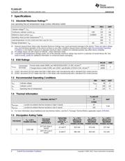
CATHODE
REF
ANODE
800Ω
2.4 kΩ
4 kΩ
20 pF
1 kΩ
7.2 kΩ
800Ω
800Ω
150Ω
10kΩ
3.28 kΩ
20 pF
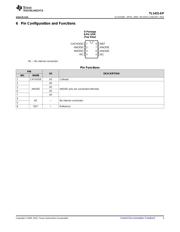
1
8
2, 3, 6, 7
REF
ANODE
CATHODE
Product
Folder
Sample &
Buy
Technical
Documents
Tools &
Software
Support &
Community
TL1431-EP
SLVS529D –APRIL 2004–REVISED JANUARY 2015
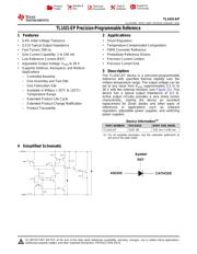
TL1431-EP Precision-Programmable Reference
1 Features 2 Applications
1
• 0.4% Initial Voltage Tolerance
• Shunt Regulators
• 0.2-Ω Typical Output Impedance • Temperature-Compensated Comparators
• Fast Turnon: 500 ns • PWM Converter Reference
• Sink Current Capability: 1 to 100 mA • Photodiode Reference Drivers
• Low Reference Current (REF) • Precision Current Limiters
• Adjustable Output Voltage: V
I(ref)
to 36 V • Precision Current Sink
• Supports Defense, Aerospace, and Medical
3 Description
Applications
The TL1431-EP device is a precision-programmable
– Controlled Baseline
reference with specified thermal stability over the
– One Assembly and Test Site
military temperature range. The output voltage can be
– One Fabrication Site
set to any value from V
I(ref)
(approximately 2.5 V) to
36 V with two external resistors (see Figure 21). This
– Available in Military (–55°C to 125°C)
device has a typical output impedance of 0.2 Ω.
Temperature Range
Active output circuitry provides a very sharp turnon
– Extended Product Life Cycle
characteristic, making the device an excellent
– Extended Product-Change Notification
replacement for Zener diodes and other types of
references in applications such as onboard
– Product Traceability
regulation, adjustable power supplies, and switching
power supplies.
Device Information
(1)
PART NUMBER PACKAGE BODY SIZE (NOM)
TL1431-EP SOIC (8) 3.91 mm × 4.90 mm
(1) For all available packages, see the orderable addendum at
the end of the data sheet.
4 Simplified Schematic
Symbol
1
An IMPORTANT NOTICE at the end of this data sheet addresses availability, warranty, changes, use in safety-critical applications,
intellectual property matters and other important disclaimers. PRODUCTION DATA.
Directory
- ・ Pinout Diagram Configuration on P3
- ・ Package Outline Dimension on P17 P19 P20
- ・ Marking Information on P17
- ・ Block Diagram on P1 P11
- ・ Typical Application Circuit Diagram on P12 P13 P14
- ・ Specification on P4
- ・ Application Area on P1 P18 P23
- ・ Electrical Specification on P5 P13 P14